8051_FPGA的实现
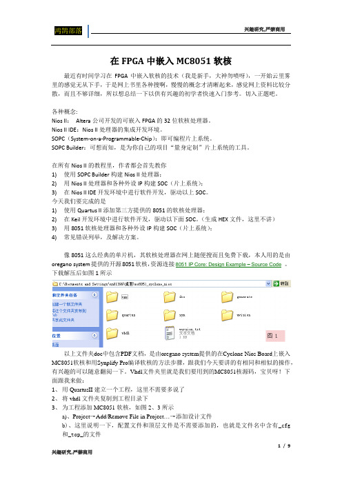
在FPGA中嵌入MC8051软核
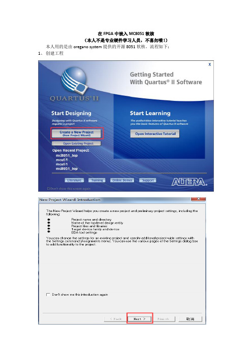
在FPGA中嵌入MC8051软核(本人不是专业硬件学习人员,不喜勿喷!)本人用的是由oregano system提供的开源8051软核。
流程如下:1、创建工程第一栏用于指定工程所在的工作库文件夹;第二栏用于指定工程名,工程名可以取任何名字,也可以直接用顶层文件的实体名作为工程名(建议使用);第三栏用于指定顶层文件的实体名。
由于是新建工程,暂无输入文件,直接NEXT注意器件的选择。
(我们老师要求EP2C35F672C6、EP2C35F672C7、EP2C35F672C8三选一)利用QuartusII的集成环境进行开发,不使用任何EDA 工具,因此这里不作任何改动。
2、添加文件(请将VHDL文件夹拷贝至工程目录下)添加文件时,配置文件和顶层文件不需要添加,也就是说带有_cfg和_top_的文件无需添加借用他人的一张图(千万不要加带有_cfg和_top_的文件)双击打开mc8051_p.vhd文件。
把mc8051_top、mc8051_ram、mc8051_ramx和mc8051_rom 的器件模块语句全部删掉并保存、关闭3、生成原理图双击打开mc8051_core_.vhd,然后File→Create/Update→Create Symbol Files for Current File →生成MC8051软核的原理图模块。
4、在工程中用原理图构建SOC(片上系统)a)、新建Block Diagram/Schematic File文件,保存并命名。
File—>newb)、双击Schematic File空白处,添加mc8051软核原理图,如图所示。
然后双击放置。
c)、生成ROM模块双击Schematic File空白处,添加ROM原理图,如图所示。
然后双击配置属性。
下图中可以为rom模块命名(如果你愿意的话)设置ROM 的信息:数据宽度8bits,数据个数4069。
取消ROM 的输出寄存器添加.hex文件d)、生成RAM模块(基本流程与ROM一致,注意点如下)选择lpm_ram_dq来生成ram模块模块命名→位宽及存储空间→取消寄存器输出→添加时钟使能→直接Finish结束设置数据宽度为8bits,数据个数为128取消RAM 的数据输出寄存器,同时选中时钟使能信号端。
基于FPGA和8051单片机IP核的多功能频率计的设计与实现
基于FPGA和8051单片机IP核的多功能频率计的
设计与实现
频率是电信号中重要的物理量,在电子、通信系统中,信号的频率稳定度决定了整个系统的性能,准确测量信号的频率是系统设计的重要内容。
单片机广泛地应用于电子系统设计,其性价比高,大量的外围接口电路,使基于单片机的电子系统设计方便,周期缩短。
然而,单片机的串行工作特点决定了它的低速性和程序跑飞,另外还存在抗干扰能力不强等缺点。
EDA(Electronic Design AutomaTIon)技术以计算机为工具,在Quartus II软件平台上,对以硬件描述语言Verilog HDL/VHDL为系统逻辑描述手段完成的设计文件,自动地完成逻辑编译、化简、综合及优化、逻辑仿真,直至对特定目标芯片的适配、编译、逻辑映射和编程下载等工作,FPGA是纯硬件结构,具有较强的抗干扰能力。
文中在FPGA芯片中嵌入MC8051 IP Core,作为控制核心,利用Verilog HDL语言进行编程,设计了以MC8051 IPCore为核心的控制模块、计数模块、锁存模块和LCD显示模块等模块电路,采用等精度测量法,实现了频率的自动测量,测量范围为0.1 Hz~50 MHz,测量误差小于0.01%。
基于51单片机和FPGA的人机交互系统的设计

基于51单片机和FPGA的人机交互系统的设计
基于51 单片机和FPGA 的人机交互系统的设计
在现代各类仪器的开发中,人机交互功能正起着无可替代的作用。
人
机交互界面友好的仪器将更容易操作和使用,从而提高工作效率。
液晶显示器(LCD)具有功耗低、价格低、寿命长、接口控制方便等特点,在科研与设计
领域正发挥着越来越大的作用。
FPGA 作为单片机外设的接口芯片,可以大大简化接口电路,通过对FPGA 进行编程,可以实现常用的译码、地址选通等功能。
本文以C8051F020 单片机与FPGA 互连系统为控制核心,以液晶显示控制器T6963C 为例,结合行扫描键盘,简述了一种人机交互功能的设计。
1 系统设计方案:
FPGA 可在很大程度上扩展单片机的资源,然而人机交互功能仍应尽量减少对单片机及FPGA 的资源消耗,以便将更多的片内资源用于其他功能的扩展。
采用FPGA 扫描键盘可以节省单片机的资源,同时也能灵活地实现键盘的扩展。
而考虑到液晶控制较复杂,依然采用单片机控制LCD,使LCD 的各种功能得到最大程度的利用,其系统框图如图1 所示。
2 硬件电路及FPGA 接口设计:
2.1 总线接口设计:
这里采用单片机C8051F020 与CycloneⅡFPGA 互连的系统。
C8051F020 器件是完全集成的混合信号系统级MCU 芯片,具有64 个数字I/O 引脚,与8051 完全兼容,而且速度得到了极大提高,70%的指令执行时间为1 或2 个系统时钟周期,只有4 条指令的执行时间大于4 个系统时钟周期。
此外,C8051F020 系列MCU 对CIP-51 内核和外设有几项关键性的改进,提高。
FPGA_8051核频率占空比可调方波输出

KX
康芯科技
KX
康芯科技
KX
康芯科技
信号输出
复位键
接示波器
KX
键2、3、4、5控制输入频率和占空比控制字
康芯科技
复位键
方波信号频率控制字显示 方波信号占空比控制字 方波信号输出至示波器
KX
信号波形输出显示
康芯科技
KX
康芯科技
多数示例提供完整源程序
KX3C10T+系统提供的大量电子设计自主创新 演示项目于宽领域大深度培养能力、启迪智慧、激励创新
杭州康芯公司
KX
康芯科技
实验7
频率和占空比可数控方波信号 发生器设计示例KX源自康芯科技注意程序路径
X 注意单片机程序路径
K
康芯科技
单片机Core程序代码
KX
康芯科技
kx康芯科技杭州康芯公司多数示例提供完整源程序kx3c10t系统提供的大量电子设计自主创新演示项目于宽领域大深度培养能力启迪智慧激励创新kx康芯科技实验7频率和占空比可数控方波信号发生器设计示例kx康芯科技注意程序路径kx康芯科技注意单片机程序路径单片机core程序代码kx康芯科技kx康芯科技kx康芯科技kx康芯科技复位键信号输出接示波器kx康芯科技方波信号输出至示波器键2345控制输入频率和占空比控制字复位键方波信号占空比控制字方波信号频率控制字显示kx康芯科技信号波形输出显示
基于FPGA中8051核等精度频率计的设计
片 上 的 技 术 。 这 样 设 计 的 好 处 是 集 成 度 高 , 不变 ,而常规 的直 测法 (在低频 时用测周期
RAM类 型 : 自动
移 植 方 便 , 还 能 集 成 各 种 功 能 , 比 如A/D转 法 ,高频时用测频 率法 ),其精度 会随着被
时 钟 类 型 : 双 时 钟 (分 开 的 输 入 输 出
如 图 3所 示 , 锁 相 环 为 软 件 自带 部 件 ,
计是在FPGA广泛应用 前一个适合 工业 生产 的 关闭 。设在一次 门控时间T 中对被测信 号计 对 其 设 置 如 下 :
方案 。单片机性价 比较高 ,但 由于其 内部资 数值为N 。对标准 频率信 号 的计数值 为N 。
1.引言
计数 器 。标 准频率信 号 (F )从COUNT1的时钟
如 图2所示 ,本设计 的IP核 于51单片机
电 子 信 号 测 量 中 最 基 本 的 测 量 之 一 就 输 入端 输入 ;被测 信 号从 COUNT2的时 钟输 基 本类似 ,端 口和功能一样 ,差别在于51单
是频率测量 ,随着 电子通 讯技术越发发 达, 入端 输入 ,设其实 际频 率为F ,测量 频率为 片机的输入输 出 口是双 向口,本 IP核 的是单
(1)RAM256
各个 模块 ,比如计数器控 制模块 ,从而 实现 同而 被测信号频率 不同的情况下 ,等精度测
输 出总 线 :8位
将 整 个 单 片 机 以 及 其 他 部 件 仿 真 在 一 片 芯 量 法 的 测 量 精 度 在 整 个 测 量 范 围 内 保 持 恒 定
存 储 容 量 :256字 长
使 用 的 设 备 :CycloneII
在FPGA中嵌入8051核的详细方法与步骤
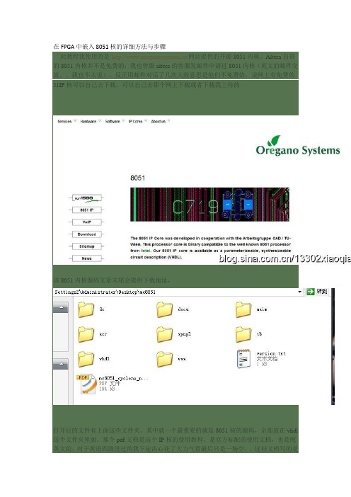
在FPGA中嵌入8051核的详细方法与步骤此教程我使用的是http://www.oreganosystems.at/网站提供的开源8051内核。
Altera自带的8051内核并不是免费的,我也曾跟altera的客服发邮件申请过8051内核(英文的邮件交流。
我也不太说),反正用邮件对话了几次大致意思是他们不免费给,说网上有免费的51IP核可以自己去下载。
可以自己去那个网上下载或者下载我上传的该8051内核源码文章末尾会提供下载地址,打开后的文件有上面这些文件夹。
其中就一个最重要的就是8051核的源码,全部放在vhdl 这个文件夹里面。
那个pdf文档是这个IP核的使用教程,是官方标配的使用文档,也是纯英文的,对于英语四级没过的我下定决心花了大力气看最后只是一场空。
这问文档写的是用Synplify Pro这个综合软件综合的,虽然据说用这个软件进行综合可以节约FPGA的很多逻辑单元,但是对于我们这些初学者来讲,真的又麻烦又不适用,我们还是直接用QuartusII 来进行综合好了。
51IP核的源码全部在都在vhdl这个文件夹中,打开是一大堆的源文件。
对于这么多的文件该怎么用,该如何使用,这是本文的重点。
首先用QuartusII建立一个工程,这这里先提醒下,文件目录最好不要包含中文,空格,不然会有些无法理解的错误。
然后将vhdl整个文件夹复制到工程目录下(个人习惯,等下添加进工程里面的时候方便点)。
下面是添加8051核文件的步骤。
选择文件添加进工程。
这里注意下后面拖着_cfg的这种文件不要添加进工程里面,还有就是含有_top_的文件也不要添加到里面。
然后双击打开mc8051_p.vhd 这个文件。
把下面这些模块的例化语句全部删掉,这点非常重要!!component mc8051_topport (clk : in std_logic;reset : in std_logic;int0_i : in std_logic_vector(C_IMPL_N_EXT-1 downto 0);int1_i : in std_logic_vector(C_IMPL_N_EXT-1 downto 0);all_t0_i : in std_logic_vector(C_IMPL_N_TMR-1 downto 0);all_t1_i : in std_logic_vector(C_IMPL_N_TMR-1 downto 0);all_rxd_i : in std_logic_vector(C_IMPL_N_SIU-1 downto 0);p0_i : in std_logic_vector(7 downto 0);p1_i : in std_logic_vector(7 downto 0);p2_i : in std_logic_vector(7 downto 0);p3_i : in std_logic_vector(7 downto 0);p0_o : out std_logic_vector(7 downto 0);p1_o : out std_logic_vector(7 downto 0);p2_o : out std_logic_vector(7 downto 0);p3_o : out std_logic_vector(7 downto 0);all_rxd_o : out std_logic_vector(C_IMPL_N_SIU-1 downto 0);all_txd_o : out std_logic_vector(C_IMPL_N_SIU-1 downto 0);all_rxdwr_o : out std_logic_vector(C_IMPL_N_SIU-1 downto 0));end component;------------------------------------------------------------------------------- START: Component declarations for simulation models-----------------------------------------------------------------------------component mc8051_ramport (clk : in std_logic;reset : in std_logic;ram_data_i : in std_logic_vector(7 downto 0);ram_data_o : out std_logic_vector(7 downto 0);ram_adr_i : in std_logic_vector(6 downto 0);ram_wr_i : in std_logic;ram_en_i : in std_logic);end component;component mc8051_ramxport (clk : in std_logic;reset : in std_logic;ram_data_i : in std_logic_vector(7 downto 0);ram_data_o : out std_logic_vector(7 downto 0);ram_adr_i : in std_logic_vector(15 downto 0);ram_wr_i : in std_logic);end component;component mc8051_romport (clk : in std_logic;reset : in std_logic;rom_data_o : out std_logic_vector(7 downto 0);rom_adr_i : in std_logic_vector(15 downto 0));end component;----------------------------------------------------------------------------- -- END: Component declarations for simulation models----------------------------------------------------------------------------- 然后双击打开mc8051_core.vhd 这个文件。
使用FPGA模拟实现8051单片机 mc8051_cyclone_nios_designflow
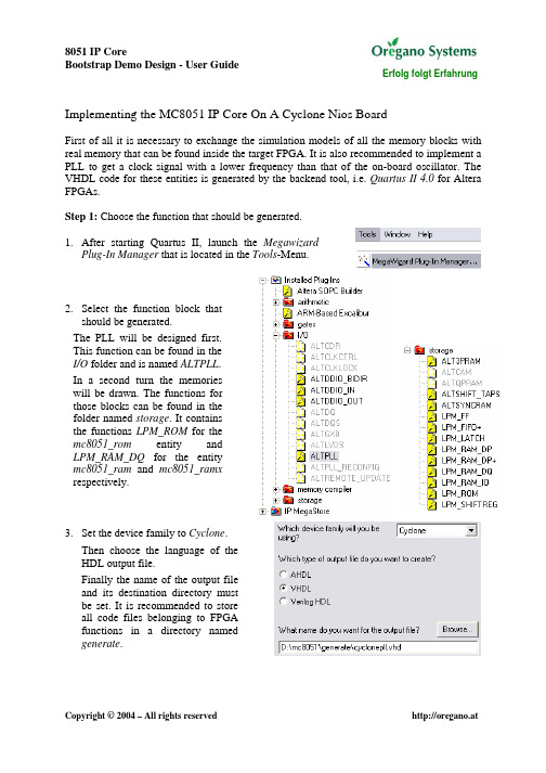
Implementing the MC8051 IP Core On A Cyclone Nios BoardFirst of all it is necessary to exchange the simulation models of all the memory blocks with real memory that can be found inside the target FPGA. It is also recommended to implement a PLL to get a clock signal with a lower frequency than that of the on-board oscillator. The VHDL code for these entities is generated by the backend tool, i.e. Quartus II 4.0 for Altera FPGAs.Step 1: Choose the function that should be generated.1.After starting Quartus II, launch the MegawizardPlug-In Manager that is located in the Tools-Menu.2.Select the function block thatshould be generated.The PLL will be designed first.This function can be found in theI/O folder and is named ALTPLL.In a second turn the memorieswill be drawn. The functions forthose blocks can be found in thefolder named storage. It containsthe functions LPM_ROM for themc8051_rom entity andLPM_RAM_DQ for the entitymc8051_ram and mc8051_ramxrespectively.3.Set the device family to Cyclone.Then choose the language of theHDL output file.Finally the name of the output fileand its destination directory mustbe set. It is recommended to storeall code files belonging to FPGAfunctions in a directory named generate.When the function has been selected and the output path has been chosen, the behaviour and the parameters of this function must be defined. This must be done for the PLL, the ROM and the internal and external RAM.Step 2: Define the behaviour and the parameters of the PLL.1.Enter the input frequency for the PLL. In the case ofthe NIOS Cyclone Board this frequency is 50 MHz.The PLL operates with an internal feedback in normal mode.2.It is also possible to add optional inputs to the PLL.To keep the design simple, none of the inputs areselected.3.If only one clock output is used,this output is automatically set toc0. Entering the value of thefrequency or selecting the factorfor the multiplication and thedivision respectively can definethe output frequency of the PLL.Be sure that the chosen settingscan be implemented which isshown at the top of the window.4.Since no other PLL outputs are selected for operation, the remaining dialogs can beskipped. Finally all files that will be generated are shown.Step 3: Define the behaviour and the parameters of the ROM.1.As the ROM is a memory function, the size of thememory and the width of the data bus have to bedefined. In the case shown at the right, the ROM isorganized 8k x 8 bit.To meet the signals of the MC8051 design, singleclocking must be used.2.The data output q of the ROM must not be registeredfor the MC8051 design since it is not supposed to be.As the ROM and the RAM blocks have designatedaddress and data busses, there is no need for a clockenable signal.3.The program file must be loaded into the memory.This can be achieved by pointing to the HEX file thatcontains the user program.4.Confirm the generation of the files.Step 4: Define the behaviour and the parameters of the internal and external RAM.1.Enter the width of the address and data bus as shown for the ROM.2.Select the behaviour of the input and output as shown for the ROM.3.Let the software decide how to implement theRAM block. If it is necessary, the RAM can bepreloaded with an additional HEX file.4.Confirm the generation of the files.Since the package file and the top level design refers to the simulation models for the memory blocks, the declaration of the ports and the wiring must be updated for exchange with the implementation models. If required the PLL must also be added to the design.Step 5: Update the component declaration in the package file.After all files for the implementation models have been generated, the component declaration for the memories in the package file mc8051_p.vhd must be updated to the entity declaration that can be found in the generated code file. For the case of the additional PLL it is also necessary to add a new component declaration for that entity. The package file should contain the following component declarations.component mc8051_ramport (address : in std_logic_vector(6 downto 0); -- address inputclock : in std_logic; -- clock inputdata : in std_logic_vector(7 downto 0); -- data inputwren : in std_logic; -- write enableq : out std_logic_vector(7 downto 0)); -- data output end component;component mc8051_ramxport (address : in std_logic_vector(12 downto 0); -- address inputclock : in std_logic; -- clock inputdata : in std_logic_vector(7 downto 0); -- data inputwren : in std_logic; -- write enableq : out std_logic_vector(7 downto 0)); -- data output end component;component mc8051_romport (address : in std_logic_vector(12 downto 0); -- address inputclock : in std_logic; -- clock inputq : out std_logic_vector(7 downto 0)); -- data output end component;component cyclonepllport (inclk0 : in std_logic; -- PLL inputc0 : out std_logic); -- PLL outputend component;Step 6: Update the wiring of the top level design.The wiring between the entities found in the top level design mc8051_top_struc.vhd also has to be updated. If the width of the address busses of the memories differs from the 16 bit wide busses provided by the MC8051 core, the smaller bus signals s_rom_adr_sml and s_ramx_adr_sml have to be inserted. If the PLL should be implemented, a new clock signal clk_pll has to be added between the PLL output and the components of the top level design. Since the switches located on the NIOS Cyclone Board are active low, the active high reset signal s_reset for the MC8051 core can be gained from the reset switch by an additional inverter.architecture struc of mc8051_top issignal s_clk_pll : std_logic; -- core clock, PLL outputsignal s_reset : std_logic; -- reset signal, active highsignal s_rom_adr_sml : std_logic_vector(12 downto 0); -- *** newsignal s_ramx_adr_sml : std_logic_vector(12 downto 0); -- *** newbegin -- architecture structurals_rom_adr_sml <= std_logic_vector(s_rom_adr(12 downto 0));s_ramx_adr_sml <= std_logic_vector(s_ramx_adr(12 downto 0));s_reset <= not reset;i_mc8051_core : mc8051_coreport map (clk => s_clk_pll, -- mc8051 corereset => s_reset,...);i_mc8051_ram : mc8051_ramport map (address => s_ram_adr, -- internal RAMclock => s_clk_pll,clken => s_ram_en,data => s_ram_data_in,wren => s_ram_wr,q => s_ram_data_out);i_mc8051_rom : mc8051_romport map (address => s_rom_adr_sml, -- ROMclock => s_clk_pll,clken => s_rom_en,q => s_pre_rom_data);i_mc8051_ramx : mc8051_ramxport map (address => s_ramx_adr_sml, -- external RAMclock => s_clk_pll,clken => s_ramx_en,data => s_ramx_data_out,wren => s_ramx_wr,q => s_ramx_data_in);i_cyclonepll : cyclonepllport map (inclk0 => clk, -- PLLc0 => s_clk_pll);When the VHDL files for the MC8051 have been changed for implementation, it is time for synthesis. Synplify Pro 7.5 is used for that steps and generates a single netlist file that can be then used for implementation.Step 7: Generate a new project file for synthesis.1.After starting Synplify Pro, open the File menu andselect New.2. A window appears where the type of the files thatshould be generated can be selected. At that point,choose Project File.3.Set the file name for the project file and point to theworking directory for Synplify Pro where the filesshould be stored.After confirming a new project will be opened.Step 8: Add the source files to the project.1.To define which source code files should be used, hitthe Add File button.2.Add the VHDL files in the followingway:First add the package file mc8051_p.vhd.Then select all files that contain theentities of the top level design. TheVHDL configuration files need not to beadded.Finally add the top level design files tothe project: mc8051_top_.vhd andmc8051_top_struc.vhd.Code files of components that depend on the target technology such as PLLs or memory blocks must not be added to the project for synthesis.3.After confirming a new folder named vhdl appears inthe project window.Step 9: Set up the implementation options.1.To choose the target technology and the file formatfor the output of the synthesis, hit the Impl Optionsbutton that is located on the left of the projectwindow.2.As the window appears, the Device folder is selected where the target FPGA can bedeclared. To implement the design for the NIOS Cyclone Board, the FPGA that is located at this board must be chosen. For that case use the options as shown above.3.It is also possible to change the output directory and the file format for the output file.Swap to the Implementation Results folder where those options are specified. If Quartus IIis used to implement the design, the file format should be set to vqm (Verilog Quartus Mapping).4.Before running the synthesis, the operating frequencyshould be entered at the project window. If a PLL isused, the frequency at the output of the PLL has to beentered.Step 10: Run the synthesis and check the warnings and the notes.1.The synthesis can be started by hitting the Run buttonwhich first runs the compiler. If there are no errors inthe VHDL code, the mapper generates the output filethat can take a few minutes.2.All messages that are produced during synthesis can be found in the SRR file located inthe output directory. These messages are divided into errors, warnings and notes. The first thing to check is which entity was selected as the top level entity. This information can be found in the notes section as shown below.Since the source file for the implementation models of the memories and the PLL depends on the target technology, they were not added for synthesis. Each entity of such a model is treated as a black box and produces a message in the warnings section.Step 11: Check the generated RTL schematic.1.The synthesis generates an RTL schematic in addition to theoutput file that can be shown via the RTL view button that islocated in the tool bar.2.Navigate through the RTL schematic to verify if thedesign is built up in a correct way. The zoomfunctions and functions to descend and ascend thehierarchy can be found in the tool bar.When entering the RTL view, the top level design is shown as above. The core of the MC8051 design and all the input and output ports are displayed whereby the entities for the PLL, the ROM and the RAMs are treated as black boxes.To descend the hierarchy, select the appropriate function from the tool bar, move the mouse cursor to the desired entity and click to swap to the next level. To ascend the hierarchy to the previous level, move the cursor next to a entity and click when an arrow that points above appears.If the design is built in a correct way, the implementation can be done. To generate the filesthat are needed to download the design to the NIOS Cyclone Board, Quartus II 4.0 is used.Step 12: Open a new project file for implementation.1.After starting Quartus II, open the File menu and startthe New Project Wizard.An introduction screen is shown before the settingsfor the implementation have to be declared.2.Choose the working directory where all the filesgenerated by Quartus II will be written to. It isrecommended to copy the VQM net list filegenerated by Synplify Pro to that directory.The name for the project and the name of thetop level entity must also be entered. This canbe easily done by pointing to the VQM net list.Take care of the name belonging to the top levelentity: there must be no underscore character atthe end of the name.3.Choose all source files for the project. As shown above, it is necessary to add the VQMnet list and all the VHDL files for the black boxes which can be found in the generate directory created before.4.Select the target technology that is used forimplementation. The NIOS Cyclone Board containsan FPGA from the Cyclone family of Altera.To get a smaller list of the FPGAs, choose speedgrade 7.The device EP1C20F400C7 can be found in the listshown on the left.5.After confirming the data given for creatingthe project file, the hierarchy of the projectis displayed on the left.The top level entity mc8051_top shouldcontain the entity mc8051_core and all theblack boxes added before.Step 13: Assign the ports of the top level entity.Before starting the compiler, it is necessary to link the ports of the design with the pins of the FPGA.1.Choose Device form the Assignments menu.In the next window, select Device & Pin Options todefine the behaviour of the pins.Since there are many components located on the NIOS Cyclone Board, it could be a problem if a unused pin drives another device. To prevent that, select the Unused Pins folder and choose that all unused pins are treated as tri-stated inputs.2.Now all ports can be linked to the pins. This can bedone manually or by loading the assignments from aTCL script.To place the pins manually, select Assign Pins in theAssignments menu.A window appears where all pins are listed. To assigna specific pin, scroll to the pin with the desirednumber, enter the name of the port in the Pin namebox and click on the Add button. Bus signals must bede-referenced with the brackets [].For example, to assign the signal p3_i[0] whichstands for the LSB of the input port 3, select the linewith pin number G15, enter the signal name as shownon the right and confirm the assignment.It is recommended to assign all ports since they arelinked randomly to a pin if the user does not assignthose ports.To load the pinassignments from a TClscript, activate the TCLConsole by selecting theappropriate command inthe View – Utility Windowsmenu.As the TCL console appears, typesource pins.tclTo load the assignments from the pins.tcl file that isdelivered with the MC8051 design.The file which contains the constraints which areloaded via the TCL console should be located in theQuartus II working directory.To use the constraints of the current project for otherdesigns, it is possible to export them to a TCL script.Select Generate TCL File for Project in the Projectmenu to generate such a file.Step 14: Run the compiler and check the errors and the warnings.To start the compiler, click on the arrow symbol that canbe found in the tool bar.A common mistake is a present underscore character at the end of the name belonging to the top level entity. In that case the following error message appears.Since the HEX file is smaller than the size of the memory used for the ROM, the remaining bytes are filled with zeros. A warning message as shown below is also forced for that case.Step 15: Configure the hardware programmer and download the bit stream to the FPGA.1.The programmer can be configured and used fordownload by selecting Programmer in the Toolsmenu.2.As the programmer appears, it is first necessary to dothe Hardware Setup.A window appears where the hardware for downloading the bit stream is listed. To set up a new device, hit the Add Hardwarebutton.If the parallel port should be used to download a bit stream via the JTAG interface, select ByteBlaster as hardware type and LPT1 asassociated port. Confirm this configuration toget back to the hardware listing.The defined hardware should now be present in thelist.For activation of that hardware, select the entry and hit the Select Hardwarebutton.3.The hardware should now also be present at the top ofthe programmer window. Set up the NIOS Cyclone Board for operation by connecting the parallel port to the JTAG interface and applying the supply voltage to the board. After that, hit the Auto Detectbutton.The programmer should now list the connected device. To add a bit stream file for download, double click on the <none> entry in the File section. A window appears where the bit stream can be selected. The SOF file mc8051_top_.sof located in the working directory for Quartus II contains the bit stream for the project.The File section should now contain the bit stream file. Check the Program/Configure flag as shown above.To start the download, hit the Start button. If there isan error during the download, an appropriate errormessage is shown.Design treegeneration of a ROM-file for simulationsynthesis with Design CompilerdocumentationVHDL code generated by Quartussimulation with Modelsimimplementation with Alteras Quartussynthesis with Synplicity’s Synplify Protestbench and memory modelssynthesizeable VHDL source codesimulation with Synopsys VSSLiteratureCyclone Device Handbook/literature/hb/cyc/cyclone_device_handbook.pdf Cyclone Nios Board, Getting Started User Guide/literature/ug/ug_nios_gsg_cyclone_1c20.pdf Cyclone Nios Board, Reference Manual/literature/manual/mnl_nios_board_cyclone_1c20.pdf。
FPGA嵌入MC8051软核的方法及常见错误分析
在FPGA中嵌入MC8051软核最近有时间学习在FPGA中嵌入软核的技术(我是新手,大神勿喷呀),一开始云里雾里的感觉无从下手,于是网上书里各种搜啊,慢慢的概念才清晰起来,感觉网上资料比较分散,而且不够详细,所以想总结一下以供有兴趣的初学者快速入门参考。
切入正题吧。
各种概念:Nios II:Altera公司开发的可嵌入FPGA的32位软核处理器。
Nios II IDE:Nios II处理器的集成开发环境。
SOPC(System-on-a-Programmable-Chip):即可编程片上系统。
SOPC Builder:可想而知,是为你自己的项目“量身定制”片上系统的工具。
在所有Nios II的教程里,作者都会首先教你1)使用SOPC Builder构建Nios II处理器;2)用Nios II处理器和各种外设IP构建SOC(片上系统);3)在Nios II IDE开发环境中进行软件开发,驱动以上SOC。
今天我们要完成的是1)使用Quartus II添加第三方提供的8051的软核处理器;2)在Keil开发环境中进行软件开发,驱动以下面SOC。
(生成HEX文件,这里不讲)3)用8051软核处理器和各种外设IP构建SOC(片上系统);4)常见错误列举,及解决方案。
像8051这么经典的单片机,其软核处理器在网上随便搜而且免费下载,本人用的是由oregano system提供的开源8051软核,。
下载解压后如图1所示以上文件夹doc中包含PDF文档,是由oregano system提供的在Cyclone Nios Board上嵌入MC8051软核和用Synplify Pro编译软核的方法步骤,跟我们今天要讲的有相同和相似的操作,有兴趣的可以随意翻阅一下。
Vhdl文件夹里就是我们要用到的MC8051核源码,宝贝呀!下面跟我来做:1、用QuartusII建立一个工程,这里不需要多说了2、将vhdl文件夹复制到工程目录下3、为工程添加MC8051软核,如图2、3所示a)、Project→Add/Remove File in Project…→添加设计文件b)、这里说明一下,配置文件和顶层文件是不需要添加的,也就是文件名中含有_cfg和_top_的文件c)、双击打开mc8051_p.vhd文件。
8051 CPLD FPGA DSP 發展系統 使用說明
8051/CPLD/FPGA/DSP發展系統使用說明一、功能與特色1. 主控元件可選用ALTERA ACEX-1K或XILINX系列等其他晶片,可模擬30,000個以上的邏輯閘,搭配MAX+PLUSⅡV10.1等發展軟體。
2. 使用硬體描述語言AHDL/VHDL及繪圖法來設計邏輯電路,方便學習。
3. 每一外接I/O PIN腳都有標示,透過外接I/O排針座可對外部實驗電路做控制,彈性空間大。
4. 頻率產生器頻率範圍:1 /10 /100 /1K /10K /100K /1M /10M /20M Hz。
5. CPLD/FPGA部份,經Printer Port 介面連線可進行燒錄。
6. 8051部份,可經由Com1或 Com2 Port 進行燒錄 (ISP) 。
7. 支援Windows作業系統。
二、 系統配件1.發展系統1組(母板1片、子板1片、Power Module 1組、Download板1組)2.光碟片1片3.25 Pin Cable線1條4.9 Pin Cable線1條5.8 Pin彩虹排線6條6.4 Pin彩虹排線4條7.2 Pin彩虹排線2條8.2 Pin Molex線1條三、電路及說明(一)切換電路此電路主要是在做PS Mode及JTAG Mode的切換,當將Switch撥 至ON,就是用PS Mode做為下載燒錄的方式,下載至EP1K30TC144-3 (當EPC2LC20壞掉時可用此法),如果Switch為OFF則是用JTAG Mode 方式來下載及燒錄,此時是將程式燒至EPC2LC20。
(二)EEPROM電路此電路主要是在JTAG Mode下會使用到,因ACEX 1K是一個RAM的架構,程式下載無法保存,所以使用一顆EEPROM配合,讓使用者能做選擇,可以將程式保存下來,也可以在實習完,將電源拿掉,程式就消失,完全看使用者的需求。
(三)ACEX 1K電路ACEX 1K 是一顆RAM架構的晶片,所以程式的下載有兩種方式,一種是PS Mode,它是直接下載到這ACEX 1K裡,另一種方式是JTAG Mode,它是將程式下載到EEPROM裡,再從EEPROM丟資料給ACEX 1K,這種方式的燒錄,程式不會因電源關掉而流失掉。
8051单片机的FPGA设计与实现
第一章前言20世纪末在计算机技术逐渐发展的情况写,电子技术得到了飞速的发展,现代电子产品已经渗透到了社会的各个领域,有力的推动了社会生产力的发展和社会信息化程度的提高,同时也使现代电子产品的性能进一步提高,产品更新换代的节奏也越来越快。
电子技术发展的根基是微电子技术的进步,它表现在大规模集成电路加工技术,即半导体工艺技术的发展上,表征半导体工艺水平的线宽已经达到60nm以下,并还在不断缩小;在硅片单位面积上集成了更多的晶体管,集成电路设计在不断地向超大规模,极低功耗和超高速的方向发展;专用集成电路ASIC (Application Specific Integrated Circuit)的设计成本不断降低,在功能上,现代的集成电路已能够实现单片电子系统SOC(System on a chip)的功能。
另外集成电路(IC)技术在微电子领域中占有重要的地位。
且伴随着IC技术的发展,电子设计自动(Electronic Design Automation,EDA)已经逐渐成为重要的设计手段,其广泛应用于模拟与数字电路系统等许多领域。
单片机是一种集成电路芯片,是采用超大规模集成电路技术把具有数据处理能力中央处理器CPU、随机存储器RAM、只读存储器ROM、多种I/O口和中断系统、定时器/计时器等功能(可能还包括显示驱动电路、脉宽调制电路、模拟多路转换器、A/D转换器等电路)集成到一块硅片上构成的一个小而完善的微型计算机系统,在工业控制领域的广泛应用。
从上世纪80年代,由当时的4位、8位单片机,发展到现在的32位300M的高速单片机。
单片机具有体积小、功耗低、控制功能强、扩展灵活、微型化和使用方便等优点,广泛应用于仪器仪表中,结合不同类型的传感器,可实现诸如电压、电流、功率、频率、湿度、温度、流量、速度、厚度、角度、长度、硬度、元素、压力等物理量的测量。
采用单片机控制使得仪器仪表数字化、智能化、微型化,且功能比起采用电子或数字电路更加强大。
MC8051单片机IP核的FPGA实现与应用
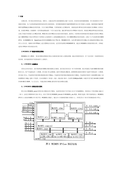
1 引言长期以来,单片机以其性价比高、体积小、功能灵活等方面的独特优点被广泛应用。
但受其内部资源的限制,单片机需要在片外扩展相关资源。
为了达到处理速度和控制灵活性方面的需求,采用微控制器和可编程逻辑器件设计单片机嵌入式系统。
随着现场可编程逻辑阵列(FPGA)及EDA技术的发展,百万门级的FPGA、可重构的嵌入式MCU核、功能复杂的IP核及各种功能强大的EDA工具的出现,实现将MCU、存储器和一些外围电路集成到一个芯片成为可能。
随着IP核技术在FPCA中的应用,特别是MCU IP核技术的发展。
出现了性能不同的嵌入式MCU软核。
MCS-51系列MCU是目前应用时间最长、最普及、可获得应用资料最多的功能强大的8位MCU,建立805l MCU可综合IP核对于各种嵌入式系统和片上系统(SOC)的应用。
针对8051MCU的应用前景,出现了几个比较典型的805l IP核,如DW8051核.OpenCore组织的0C8051核及T51核,MC805l核等。
这些IP核都是采用HDL语言描述的软MCU内核,其与工艺无关,能够在多种FPGA上进行逻辑综合及实现。
这里采用免费的MC805lIP核,通过对MC8051结构原理的分析,详细论述其在FPCA中的实现及应用。
2 MC8051 IP核基本结构及原理MC8051是与MCS一5l系列微处理器指令集完全兼容的8位嵌入式微处理器,通过芯核重用技术,可广泛应用在一些面积要求比较苛刻,而对速度要求不是很高的片上系统中。
2.1 MC8051功能特点采用完全同步设计:指令集和标准8051微控制器完全兼容;指令执行时间为l~4个时钟周期,执行性能优于标准805l微控制器8倍左右;用户可选择定时/计数器、串行接口单元的数量,最多可增加到256组;新增特殊功能寄存器用于选择不同的定时/计数器、串行接口单元;可选择是否使用乘法器(乘法指令MUL);可选择是否使用除法器(除法指令DIV);可选择是否使用十进制调整功能(十进制调整指令DA);I/0口不复用,无双向数据I/O端口,输入、输出端口独立;内部带256Byte RAM;⑾最多可扩展至64 KB的ROM 和64 KB的RAM;与工艺无关,可通过修改VHDL源代码扩展及参数化设置。
8051_FPGA的实现

28
三种描述方式的比较
描述方式 结构化描述 优点 缺点 适用场合
数据流描述 行为描述
连接关系清 电路不易理解、 电路层次化设 计 晰,电路模 繁琐、复杂 块化清晰 布尔函数定 不易描述复杂电 小门数设计 义明白 路,修改不易 电路特性清 进行综合效率相 大型复杂的电 楚明了 对较低 路模块设计
29
地址总线(低8位) 数据总线 双向I/o端口
/PSEN ALE /EA /RST
双向I/o端口
双向I/o端口
RD WR T1 T0 INT1 INT0 TXD RXD
P3.7 P3.6 P3.5 P3.4 P3.3 P3.2 P3.1 P3.0
A15 A14 A13 A12 A11 A10 A9 A8
4. 变址寻址
17
VHDL硬件描述语言
概述 基本语法
18
VHDL简介
美国国防部在80年代初提出了VHSIC (Very High Speed Integrated Circuit)计划 VHDL已成为国际的硬件描述语言标准
19
VHDL的特点
适用于复杂的、多层次的设计 与硬件独立 有丰富的软件支持 其设计便于向ASIC过渡
RD P3 P2 WR
= 64KB
译码
/CE WR /OE
13
8051指令系统
指令分类
指令格式
寻址方式
14
8051指令按功能划分为5组
1. 数据传送指令 2. 算术运算指令 3. 逻辑运算指令 4. 布尔操作(位操作)指令
5. 控制转移指令
15
指令格式
无操作数的单字节指令: NOP 操作码 操作数域 1 操作数域 2
VHDL与计算机语言的区别
MC8051 FPGA实验
实验三:MC8051 FPGA实验甯兵0842023038 程序如下:1、ROM:LIBRARY ieee;USE ieee.std_logic_1164.all;LIBRARY altera_mf;USE altera_mf.all;ENTITY mc8051_rom ISPORT(address : IN STD_LOGIC_VECTOR (12 DOWNTO 0);clock : IN STD_LOGIC ;q : OUT STD_LOGIC_VECTOR (7 DOWNTO 0));END mc8051_rom;ARCHITECTURE SYN OF mc8051_rom ISSIGNAL sub_wire0 : STD_LOGIC_VECTOR (7 DOWNTO 0);COMPONENT altsyncramGENERIC (address_aclr_a : STRING;init_file : STRING;intended_device_family : STRING;lpm_hint : STRING;lpm_type : STRING;numwords_a : NA TURAL;operation_mode : STRING;outdata_aclr_a : STRING;outdata_reg_a : STRING;widthad_a : NA TURAL;width_a : NA TURAL;width_byteena_a : NA TURAL);PORT (clock0 : IN STD_LOGIC ;address_a : IN STD_LOGIC_VECTOR (12 DOWNTO 0);q_a : OUT STD_LOGIC_VECTOR (7 DOWNTO 0));END COMPONENT;BEGINq <= sub_wire0(7 DOWNTO 0);altsyncram_component : altsyncramGENERIC MAP (address_aclr_a => "NONE",init_file => "file.hex",intended_device_family => "Cyclone",lpm_hint => "ENABLE_RUNTIME_MOD=NO",lpm_type => "altsyncram",numwords_a => 8192,operation_mode => "ROM",outdata_aclr_a => "NONE",outdata_reg_a => "UNREGISTERED",widthad_a => 13,width_a => 8,width_byteena_a => 1)PORT MAP (clock0 => clock,address_a => address,q_a => sub_wire0);END SYN;2、RAM:LIBRARY ieee;USE ieee.std_logic_1164.all;LIBRARY altera_mf;USE altera_mf.all;ENTITY mc8051_ram ISPORT(address : IN STD_LOGIC_VECTOR (6 DOWNTO 0);clock : IN STD_LOGIC ;data : IN STD_LOGIC_VECTOR (7 DOWNTO 0);wren : IN STD_LOGIC ;q : OUT STD_LOGIC_VECTOR (7 DOWNTO 0) );END mc8051_ram;ARCHITECTURE SYN OF mc8051_ram ISSIGNAL sub_wire0 : STD_LOGIC_VECTOR (7 DOWNTO 0);COMPONENT altsyncramGENERIC (clock_enable_input_a : STRING;clock_enable_output_a : STRING;intended_device_family : STRING;lpm_hint : STRING;lpm_type : STRING;numwords_a : NA TURAL;operation_mode : STRING;outdata_aclr_a : STRING;outdata_reg_a : STRING;power_up_uninitialized : STRING;widthad_a : NA TURAL;width_a : NA TURAL;width_byteena_a : NA TURAL);PORT (wren_a : IN STD_LOGIC ;clock0 : IN STD_LOGIC ;address_a : IN STD_LOGIC_VECTOR (6 DOWNTO 0);q_a : OUT STD_LOGIC_VECTOR (7 DOWNTO 0);data_a : IN STD_LOGIC_VECTOR (7 DOWNTO 0) );END COMPONENT;BEGINq <= sub_wire0(7 DOWNTO 0);altsyncram_component : altsyncramGENERIC MAP (clock_enable_input_a => "BYPASS",clock_enable_output_a => "BYPASS",intended_device_family => "Cyclone II",lpm_hint => "ENABLE_RUNTIME_MOD=NO",lpm_type => "altsyncram",numwords_a => 128,operation_mode => "SINGLE_PORT",outdata_aclr_a => "NONE",outdata_reg_a => "UNREGISTERED",power_up_uninitialized => "TRUE",widthad_a => 7,width_a => 8,width_byteena_a => 1)PORT MAP (wren_a => wren,clock0 => clock,address_a => address,data_a => data,q_a => sub_wire0);END SYN;3、RAMXLIBRARY ieee;USE ieee.std_logic_1164.all;LIBRARY altera_mf;USE altera_mf.all;ENTITY mc8051_ramx ISPORT(address : IN STD_LOGIC_VECTOR (12 DOWNTO 0);clock : IN STD_LOGIC ;data : IN STD_LOGIC_VECTOR (7 DOWNTO 0);wren : IN STD_LOGIC ;q : OUT STD_LOGIC_VECTOR (7 DOWNTO 0) );END mc8051_ramx;ARCHITECTURE SYN OF mc8051_ramx ISSIGNAL sub_wire0 : STD_LOGIC_VECTOR (7 DOWNTO 0);COMPONENT altsyncramGENERIC (address_aclr_a : STRING;indata_aclr_a : STRING;intended_device_family : STRING;lpm_hint : STRING;lpm_type : STRING;numwords_a : NA TURAL;operation_mode : STRING;outdata_aclr_a : STRING;outdata_reg_a : STRING;power_up_uninitialized : STRING;widthad_a : NA TURAL;width_a : NA TURAL;width_byteena_a : NA TURAL;wrcontrol_aclr_a : STRING);PORT (wren_a : IN STD_LOGIC ;clock0 : IN STD_LOGIC ;address_a : IN STD_LOGIC_VECTOR (12 DOWNTO 0);q_a : OUT STD_LOGIC_VECTOR (7 DOWNTO 0);data_a : IN STD_LOGIC_VECTOR (7 DOWNTO 0) );END COMPONENT;BEGINq <= sub_wire0(7 DOWNTO 0);altsyncram_component : altsyncramGENERIC MAP (address_aclr_a => "NONE",indata_aclr_a => "NONE",intended_device_family => "Cyclone",lpm_hint => "ENABLE_RUNTIME_MOD=NO",lpm_type => "altsyncram",numwords_a => 8192,operation_mode => "SINGLE_PORT",outdata_aclr_a => "NONE",outdata_reg_a => "UNREGISTERED",power_up_uninitialized => "TRUE",widthad_a => 13,width_a => 8,width_byteena_a => 1,wrcontrol_aclr_a => "NONE")PORT MAP (wren_a => wren,clock0 => clock,address_a => address,data_a => data,q_a => sub_wire0);END SYN;RTL 网表:综合报告:时序报告:。
基于IP核的嵌入式8051VHDL设计及FPGA实现
设计 , 而是设 计 如何 跟 上芯 片设 计 复 杂 性 的增 长 步
伐 , 及 如 何 满 足 激 烈 的 市 场 竞 争 对 产 品 上 市 时 间 以
越来 越苛刻 的 要求. 片 上 系统 设 计 变 得异 常 复 杂 在
关 键 词 :I ; P棱 设计 ; P F GA实 现
中 图 分 类 号 : N 42 T 0 随着 超 大 规 模集 成 电 路 ( S ) 艺 的进 展 , VL I 工 集 成 电 路 的集 成 度 按 摩 尔 定 律 所 预 言 的 速 度 不 断 增 加 , 上 系 统 ( O 的 规 模 越 来 越 大 . 入 深 亚 微 米 片 S C) 进 以 后 . 题 已不 在 是 单 个 芯 片 是 否 有 能 力 容 纳 系 统 问
I 一般采 用 VHDL或 V r o P核 e i g语 言描述 、 [ 网 表描述 ( el t 和 版 图 描 述 (a o 1 三 种 形 式 . n ts ) i 1y u ) 其
中 , 用 VHDL或 V rlg语 言 描 述 相 当 于 “ ” 采 ei o 软 内
核, 由于其 与工 艺无关 , 故应 用最 灵活. I E NT L公 司 的 MC 一 I系 列 MC 可 以说 是 S5 U
C U 核两 部 分组 成 , 中外 围电路 包括 IO 串 口 、 P 其 / 定时器 和 Wac d g监 视 电路等. th o 本文 的 C U 核 采 P
用 了 S npy y o ss公 司 所 提 供 的 d 8 5 - oeI 核 , w 0 l c r P
识, 极大 地 降低 了设计 成 本 , 缩短 了设 计 周期 , 为 成
基于fpga的8051ip核的设计与验证研究
苏州大学硕士学位论文基于FPGA的8051IP核的设计与验证研究姓名:薛迎春申请学位级别:硕士专业:电子与通信工程指导教师:胡剑凌2010-12-31基于FPGA的8051IP核的设计与验证研究中文摘要基于FPGA的8051IP核的设计与验证研究中文摘要单片机自1976年问世以来,作为微型计算机一个很重要的分支,受到了人们的广泛关注和重视,尤其是美国Intel公司生产的MCS-51系列单片机,由于其具有集成度高、处理功能强、可靠性高、系统结构简单、价格低廉等优点,在我国已经得到了非常广泛的应用。
本论文主要的研究任务就是以8051单片机为蓝本,并与FPGA 内部结构相结合,使用硬件描述语言VHDL来实现整个系统的逻辑描述,开发出能够应用于FPGA的8051IP核。
本论文首先介绍了FPGA的相关基本知识和EDA开发工具,对8051单片机进行原理分析及各模块的功能介绍。
利用自顶向下的设计方法对8051CPU进行了IP核模块划分,对各模块进行了VHDL编程实现,设计了相应的测试数据,在modelsim仿真平台上完成了各模块的时序和功能验证,所实现的指令系统与8051单片机的指令系统完全兼容,实现了预期的效果。
论文最后在Altera公司的EP1K100FC484芯片上对整个8051IP核进行了综合仿真,搭建了简单的应用电路,完成了IP核的验证。
本论文在阐述可编程逻辑器件及其发展的基础上,结合了国内外对FPGA的使用限制,引出了在FPGA上开发嵌入式模块程序的理念并提出了设计实现方法和验证实例。
该设计具有很高的实用性,可以促进单片机技术和可编程逻辑器件课程的教学工作。
实现的8051IP核也可以在某些方面加快教育信息化的发展,进一步扩大了可编程逻辑器件的使用范围,将复杂专有芯片推向高端和超复杂应用,使得IP资源复用理念得到更普通的应用,为基于FPGA的嵌入式系统设计提供了广阔的思路。
关键词:FPGA、VHDL、8051 IP核作者:薛迎春指导教师:胡剑凌Abstract design and verification of 8051IP core based on FPGA Design and Verification of 8051IP Core Based on FPGAAbstractAs a very important branch of computer, single-chip microcomputer(SCM) has received significant attention since it was invented in 1976. Particularly the MCS-51 series SCM which was produced by the USA Intel company, has been widely used in varies industries in our country for its high integration, robustness, flexibility, low cost, and so on. This thesis implements the IP core of 8051 MCU using VHDL, and the FPGA is selected as the simulation platform.This paper firstly introduces the related basic knowledge of FPGA and the development tools of EDA, the principle analysis of 8051SCM and the function of each module. By using top-down design method for 8051 CPU conducted IP core module partition, using VHDL language to program of each module, and designing the corresponding test data. In the modelsim simulation platform, the timing and function verification of each module were completed. The accomplished instruction set is fully compatible with the 8051 single-chip Microsoft instruction, so this design is achieved the desired result. Finally, this paper conducted a comprehensive simulation to the whole 80C51IP core in Altera company EP1K100FC484 chip, and built a simple application circuit to complete the IP core validation.The realization of 8051IP core can accelerate the development of education informatization in some respect, and further expand the programmable logic devices scope of application, complex proprietary chip to high-end and complicated application, making the concept of IP resources to be more reuse common application, the application of the embedded system based on FPGA design provides a broad avenue of research. Keywords: FPGA, VHDL, 8051 IP coreWritten by Xue YingchunSupervised by Hu Jianling基于FPGA的8051IP核的设计与验证研究第一章前言第一章前言单片机的出现是计算机技术的里程碑事件,因为单片机的诞生标志着计算机正式形成了通用计算机系统和嵌入式计算机系统两大分支。
基于FPGA的8051IP核的设计与实现
基于FPGA的8051IP核的设计与实现
徐慧;王金海;王巍
【期刊名称】《计算机技术与发展》
【年(卷),期】2009(19)3
【摘要】裁减并完善了与MCS-51系列微处理器指令集完全兼容的8051IP核,减少了设计面积,提高了处理速度.按照自顶而下的设计原则,分别设计了算术逻辑单元、中心控制器、定时/计数器、串行口、RAM和ROM单元.设计采用VHDL语言进
行描述并且用ModelsimSE6.0进行功能和时序验证.将8051IP核下载到Xilinx公司的FPGA(XC3SSOOE-4FG320C)上进行物理验证,测试了一个LED流水灯程序,
结果表明软核达到预期的效果.本设计作为可移植的IP核,可以组成片上系统,用于
嵌入式系统领域.
【总页数】4页(P42-45)
【作者】徐慧;王金海;王巍
【作者单位】天津工业大学,信息与通信工程学院,天津,300160;天津工业大学,信息与通信工程学院,天津,300160;天津工业大学,信息与通信工程学院,天津,300160【正文语种】中文
【中图分类】TP302
【相关文献】
1.基于Xilinx FPGA IP核的浮点频域脉冲压缩算法的设计与实现 [J], 邢冠培;孟凡利
2.基于FPGA与8051IP核的宽带数字频率计系统设计 [J], 孙锐;朱军;丁大为;
3.基于FPGA与8051IP核的宽带数字频率计系统设计 [J], 孙锐;朱军;丁大为
4.基于FPGA的模板滤波IP核的设计与实现 [J], 李东;敖晟;田劲东;田勇
5.基于FPGA IP核的FIR滤波器设计与实现 [J], 李奇;尹倩;姚硕;孙杨
因版权原因,仅展示原文概要,查看原文内容请购买。
基于FPGA的增强型MC8051的设计
I l 一
图 1 0 l 框 图 85 的
门阵列 , 它是在 P L G L、 P D等 可编程 器件 的基础 上进 A 、A CL
一
步 发展 的产物 。它 是作 为专 用集 成 电路 ( I ) ASC 领域 中 的
种 半定 制 电路 而 出现 的, 既解 决 了定 制 电路 的不足 , 又克
f通过特 殊的 寄存 器控制 定时器和 串口 、
2 2 2 设 计 框 图 ..
如 图 1 示 ,0 1 片机主 要 由内部 R M 、 M、 部 所 85 单 A RO 外 R MX和 8 5 A 0 1核 组成 ,其 中 8 5 0 1核 由算术 逻 辑 单 元 、 串 口、 定时器 、0 1 制器组 成 , 有 7 85 控 共 4个引脚 ;
应 技与 究 圆 甭 术研 医
C 0 85 1的设 计
306) 0 1 0
’
) 码进行 修 改 , L代 增加 P L锁 相环 功 能 , 内部 R L 将 AM 除法 器以得到增 强型的 5 核 。 1
王
I儿 I
目_ ・ : = , — 皇 芒 ! i 皇 巳 4
_
c o k sg a l c i n l
r st e e
-・ ・-
r s tsg a e e i l n
—
ra m
— ・- ・
dt i a a
—
:i t l g c n sd o i
_ _
vc r7 o no0; et ( w t ) o d
d t p t a ai u n
_ _
..
..
a r se d ess
w r
— ~
在FPGA上对OC8051IP核的修改与测试
在FPGA上对OC8051IP核的修改与测试引言20 世纪80 年代初,Intel 公司推出了MCS-51 单片机,随后Intel 以专利转让的形式把8051 内核发布给许多半导体厂家,从而出现了许多与MCS-51系统兼容的产品。
这些产品与MCS-51 的系统结构相同,采用CMOS 工艺,因而常用80C51 系列来指代所有具有8051 指令系统的单片机。
在80C51 系列中,OC8051 以架构清晰、取指带宽大、时钟效率高等诸多优点受到业内人士的青睐。
本文在分析OpenCores 网站提供的一款OC8051IP 核的基础上,给出了一种仿真调试方案;利用该方案指出了其中若干逻辑错误并对其进行修改,最终完成了修改后IP 核的FPGA 下载测试。
1 OC8051 结构分析OpenCores 网站提供的OC8051 IP 核与8051 的系统结构相同,如图1 所示。
该IP 核兼容所有8051 指令系统,内部资源包括:8 位CPU,寻址能力达2×64K;4 KB 的ROM 和128 字节的RAM;4 个8 位I/O 口;16 位内部定时/计数器;5 个中断源和2 个中断优先级。
采用Verilog 语言对其各个模块进行描述。
系统主要模块及其功能说明如表1 所列。
不同模块对应的源文件均是以模块名称命名的,例如累加器A 对应的源文件为oc8051_acc.v。
虽然上述OC8051 IP 核宣称兼容所有8051 指令系统,但是实际执行时并非如此。
例如在执行表2 所列的2 组功能相同的代码时,所得到的执行结果并不相同。
代码1 的执行结果是将5 写入地址为0 的外部RAM,代码2 的执行结果是将5 写入地址为4 的外部RAM。
造成这种现象的原因是,。
利用FPGA IP平台实现基于8051微控制器的SoC
利用FPGA IP平台实现基于8051微控制器的SoC
lan Land
【期刊名称】《世界电子元器件》
【年(卷),期】2005(000)003
【摘要】一直以来,从事消费电子、汽车电子等要求快速上市的产品的设计人员,都面临着设计时间缩短的巨大压力。
现在,这种对时间要求比较苛刻的项目设计已经向其他领域转移,包括嵌入式控制和工业设计。
加速产品的上市时间越来越重要,产品销售每推迟一周,对生产商就意味着很大的经济损失。
举个例子,如果某产品的平均售价为1500美元,
【总页数】4页(P24-27)
【作者】lan Land
【作者单位】Actel公司
【正文语种】中文
【中图分类】TN919.81
【相关文献】
1.一种基于FPGA的流水线8051 IP核的设计与实现 [J], 王发栋;杜慧玲;史翔
2.基于FPGA的8051IP核的设计与实现 [J], 徐慧;王金海;王巍
3.基于SoC FPGA的MIPS处理器验证平台设计 [J], 张伟;梁蓓;
4.基于 IP 核的嵌入式8051 VHDL设计及FPGA实现 [J], 卢贵主;周剑扬;夏斐斐;
陈辉煌
5.基于FPGA的SoC/IP验证平台的应用 [J], 郭新刚; 田泽
因版权原因,仅展示原文概要,查看原文内容请购买。
- 1、下载文档前请自行甄别文档内容的完整性,平台不提供额外的编辑、内容补充、找答案等附加服务。
- 2、"仅部分预览"的文档,不可在线预览部分如存在完整性等问题,可反馈申请退款(可完整预览的文档不适用该条件!)。
- 3、如文档侵犯您的权益,请联系客服反馈,我们会尽快为您处理(人工客服工作时间:9:00-18:30)。
地址总线(低8位) 数据总线 双向I/o端口
/PSEN ALE /EA /RST
双向I/o端口
双向I/o端口
RD WR T1 T0 INT1 INT0 TXD RXD
P3.7 P3.6 P3.5 P3.4 P3.3 P3.2 P3.1 P3.0
A15 A14 A13 A12 A11 A10 A9 A8
p2_i
p3_i
核心模块
顶层模块
RAM
ROM
RAM
40
顶层(TOP)模块划分
8051核心模块
内部RAM模块 内部ROM模块
外部RAM模块
41
8051核心模块划分
ALU模块 串行控制器模块
定时/计数器模块
控制器模块
42
8051模块分层结构
8051顶层 内部RAM 定时/计时器 外部RAM ALU 8051核心 串行控制器 加、减法运算 乘法运算 内部ROM 控制器 有限状态机 存储控制
33
器件标识
34
8051的设计与实现
设计流程
难点分析
设计验证
35
设计流程
确定指标 架构规划
时序规划
模块实现 设计验证
36
8051设计的主要指标
8位CPU
128 B的片内数据RAM
最多4 KB的片内程序ROM 4个8位双向I/O端口
指令集的部分实现
37
设计难点
模块的划分 控制器的实现
38
模块划分原则
P0 : 兼做数据、地址总线 P2 : 地址总线
11
片内数据存储器
FF
高 128
80 7F
特殊功能寄存器 SFR Special Function Registers
低 128
00
12
8051使用外部扩展数据存储器
P1 P0
8 0 5 1
RAM
LATCH
ALE
Addr 216 ( 0~64KB)
划分后最底层的逻辑块应适合用逻辑语
言进行表达
相似的功能应设计成共享的基本模块
接口信号尽可能少
同层次的模块之间在资源和I/O分配上尽 可能平衡
39
8051模块示意图
clk reset all_t0_i all_t1_i all_rxd_i int0_i int1_i p0_i p1_i 控 制 器 p0_o p1_o p2_o p3_o ALU 串行控制器 串行控制器 定时/计数器 定时/计数器 all_rxdwr_o all_txd_o all_rxd_o
VHDL与计算机语言的区别
运行的基础
– 计算机语言是在CPU+RAM构建的平台上运行 – VHDL设计的结果是由具体的逻辑、触发器组成的 数字电路
执行方式
– 计算机语言基本上以串行的方式执行 – VHDL在总体上是以并行方式工作
验证方式
– 计算机语言主要关注于变量值的变化 – VHDL要实现严格的时序逻辑关系
30
FPGA器件
FPGA 现场可编程门阵列 Field Programmable Gate Array 主要生产厂商 Xilinx Altera
31
FPGA开发板
32
开发板主要部件
FPGA Xilinx® Spartan-IIE XC2S200E6FT256C SPROM Xilinx XC18V02VQ44C 50 MHz oscillator
2 x 16 –Bit
2 x 16 –Bit 3 x 16 -Bit 3 x 16 –Bit 3 x 16 –Bit
5
5 6 6 6
5
MCS-51 引脚说明
P0.7 P0.6 P0.5 P0.4 P0.3 P0.2 P0.1 P0.0 P1.7 P1.6 P1.5 P1.4 P1.3 P1.2 P1.1 P1.0 P2.7 P2.6 P2.5 P2.4 P2.3 P2.2 P2.1 P2.0 AD7 AD6 AD5 AD4 AD3 AD2 AD1 AD0
每行以;结尾 关键字end 后跟实体名 关键字begin 关键字end后 跟构造体名
22
构造体
实体(Entity)
描述设计功能的输入输出端口
在层次化设计时,端口为模块之间的 接口 在芯片级,端口代表具体芯片的管脚
23
A[3..0] equal
B[3..0]
Entity eqcomp4 is port(a, b: in std_logic_vector(3 downto 0); equal:out std_logic ); end eqcomp4;
多路选通
43
各模块占用资源的统计数据
模 名 块 称 组合逻辑 (slice) 1671 996 137 966 881 时序逻辑 (触发器) 1417 364 8 351 1032 I/O端口 bit 65 114 52 158 26 最高时 钟频率 MHZ 39.4 35.9 33.3 40.1 155.7 综 合 时 间 秒 153 56 8 54 62 占用率 % 71 42 5 41 37
10
使用外部程序存储器的例子
读回数据87h
读出地址为 0421h 单元中字节(87h)
P1
P0
EPROM
8 /EA 0 5 1 ALE
P3 P2 /PSEN
LATCH
Addr
/OE
高8位地址 : 04h 低8位地址 : 21h
EA : EA :
接高电平使用片内程序存储器 接低电平使用片外扩展程序存储器
高层次的功能描述, 不必考虑在电路中到 底是怎样实现的。
26
结构体--数据流描述
Architecture dataflow1 of eqcomp4 is begin equal <= ‘1’ when a=b else ‘0’; end dataflow1;
描述输入信号经过怎样 的变换得到输出信号。 当a和b的宽度发生变化 时,需要修改设计,当 宽度过大时,设计非常 繁琐
RD P3 P2 WR
= 64KB
译码
/CE WR /OE
13
8051指令系统
指令分类
指令格式
寻址方式
14
8051指令按功能划分为5组
1. 数据传送指令 2. 算术运算指令 3. 逻辑运算指令 4. 布尔操作(位操作)指令
5. 控制转移指令
15
指令格式
无操作数的单字节指令: NOP 操作码 操作数域 1 操作数域 2
27
结构体--结构化描述
architecture struct of eqcomp4 is begin U0:xnor2 port map(a(0),b(0),x(0)); U1:xnor2 port map(a(1),b(1),x(1)); U2:xnor2 port map(a(2),b(2),x(2)); U3:xnor2 port map(a(3),b(3),x(3)); U4:and4 port map(x(0),x(1),x(2),x(3),equal); end struct; 类似于电路的网络表,将各器件 通过语言的形式进行连接,与电 路有一一对应的关系。 一般用于大规模电路的层次化设 计时。
4
MCS-51 产品系列
引脚完全兼容
型 号
8031AH 8051AH 8051AHP 8751H NONE
片内存储器
程序存储器 数据存储器 128x8 RAM 128x8 RAM 128x8 RAM 128x8 RAM
定时器
2 x 16 -Bit 2 x 16 –Bit 2 x 16 –Bit 2 x 16 –Bit
4. 变址寻址
17
VHDL硬件描述语言
概述 基本语法
18
VHDL简介
美国国防部在80年代初提出了VHSIC (Very High Speed Integrated Circuit)计划 VHDL已成为国际的硬件描述语言标准
19
VHDL的特点
适用于复杂的、多层次的设计 与硬件独立 有丰富的软件支持 其设计便于向ASIC过渡
含一个操作地址的单字节指令: CLR C
含两个操作地址的单字节指令: MOV A, Rn
含一个操作地址的双字节指令: SJMP rel
含两个操作地址的三字节指令: LJMP addr16
16
指令的寻址方式
1. 立即数寻址
2. 直接寻址 5. 寄存器间接寻址 6. 相对寻址 7. 位寻址
3. 寄存器寻址
中 断
5 5 5 5
4Kx8 ROM 4Kx8 ROM 4Kx8 EPROM
8751H-8
8751BH 8032AH 8052AH 8752BH
4Kx8 EPROM
4Kx8 EPROM NONE 8Kx8 ROM 8Kx8 EPROM
128x8 RAM
128x8 RAM 256x8 RAM 256x8 RAM 256x8 RAM
可读性好
20
VHDL数据对象(DataObjects)
常量 变量 信号 文件(93版新增)
21
VHDL 程序代码的例
eqcomp4.vhd 库 包 实体
--eqcomp4 is a four bit equality comparator
文件名和实体 名一致
Library IEEE; use IEEE.std_logic_1164.all; entity eqcomp4 is port(a, b:in std_logic_vector(3 downto 0); equal :out std_logic); end eqcomp4; architecture dataflow of eqcomp4 is begin equal <= ‘1’ when a=b else ‘0’; End dataflow;