微波仿真论坛_matlab feko
MATLAB论坛

3.MATLAB技术论坛有丰富的MATLAB电子资源,我们秉承着互联网免费共享的精神,为大家提供相关教学资料。
4.MATLAB技术论坛拥有强大技术团队、高效严谨的管理团队,能够及时高效的为大家提供免费的技术交流和在线解答。
MATLAB技术论坛是目前国内优秀、专业和权威的MATLAB技术学习和交流平台!致力为网友提供丰富的MATLAB教学资源、强大的MATLAB技术支持和全面的MATLAB有偿服务!
网站涵盖MATLAB视频教学,MATLAB下载安装,MATLAB经典教程,Simulink仿真科技,MATLAB函数速查,MATLAB汉化包,MATLAB电子期刊,MATLAB读书频道,GUI界面开发,统计概率,拟合优化,混合编程,GPU高性能计算,神经网络,遗传算法,控制系统,图像处理,经济金融,信号通信,医药生物,数学建模,电子电力,汽车设计等几十个B技术论坛目的是为学习和使用MATLAB的网友提供一个最优秀、专业和权威的技术交流平台。
2.MATLAB技术论坛学习、交流、讨论的大门永远向大家敞开着,我们欢迎任何热爱Matlab的网友加入我们,正如我们说的 love Matlab love Matlabsky !
本试题下载由MATLAB技术论坛提供带宽。
官方网址: net/cn/org
服务邮箱:matlabsky@
在线客服:1341692017
MATLAB技术论坛(Simulink仿真论坛)由西北工业大学航空学院dynamic同学于2008年09月14日创建,并在2010.08.01对论坛管理结构进行扩充和重组,新加入6名(yaksa,matsuper,yangzijiang,faruto,rocwoods,xiezhh)MATLAB高级爱好者!
微波仿真论坛_Microstrip Bandstop and Lowpass Filters
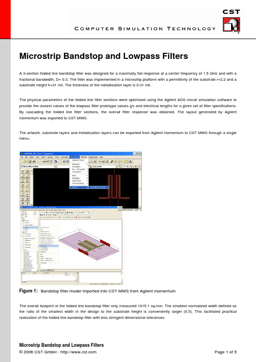
Microstrip Bandstop and Lowpass FiltersA 3-section folded line bandstop filter was designed for a maximally flat response at a center frequency of 1.5 GHz and with a fractional bandwidth, D= 0.3. The filter was implemented in a microstrip platform with a permittivity of the substrate r=2.2 and a substrate height h=31 mil. The thickness of the metallization layer is 0.31 mil.The physical parameters of the folded line filter sections were optimized using the Agilent ADS circuit simulation software to provide the closest values of the lowpass filter prototype values g's and electrical lengths for a given set of filter specifications.line filter sections, the overall filter response was obtained. The layout generated by Agilent momentum was exported to CST MWS.Figure 1:Bandstop filter model imported into CST MWS from Agilent momentumThe overall footprint of the folded line bandstop filter only measured 1015.1 sq.mm. The smallest normalized width defined as the ratio of the smallest width in the design to the substrate height isrealization of the folded line bandstop filter with less stringent dimensional tolerances.Figure 2:Response comparison for the folded line bandstop filterFigure 2 shows a comparison of the circuit simulation results using Agilent ADS with the full wave EM simulation results using CST MWS and Agilent momentum. The time domain solver was used in the case of CST MWS. Further validation is provided with the help of the measured results. The S-parameters are shown between 0.5 to 2.5 GHz. The bandstop behavior can be clearly seen between 1.4 to 1.6 GHz.Figure 3:Surface current in the stopband at 1.5 GHzFigure 4:Surface current in the lower passband at 1.0 GHzSimilarly, a 3-section folded line lowpass filter was designed for a maximally flat response with a cut-off frequency of 1.5 GHz. The folded line lowpass filter was also implemented in a microstripFigure 5:3D view of the folded line lowpass filterFigure 6 shows a comparison of the circuit simulation results for the folded line lowpass filter using Agilent ADS with the fullFigure 6:Response comparison for the folded line lowpass filter Figure 7:Surface current in the passband at 1.0 GHzFigure 8:Surface current in the stopband at 2.0 GHz References。
微波仿真论坛_阵列天线的FEKO仿真分析概要
第18卷第1期2009年3月计算机辅助工程Computer A ided EngineeringVol . 18No . 1Mar . 2009・安世亚太软件应用・文章编号:1006-0871(2009 0120073205阵列天线的FEK O 仿真分析刘源, 焦金龙(安世亚太科技(北京有限公司, 北京100026摘要:为在有限的硬件资源下, 对复杂单元的大规模阵列天线进行有效分析,提出采用FEK O 软件分析任意大规模阵列天线的有效方法. 首先应用FEK O 进行相控阵分析, 然后根据阵列天线的单元激励方向图(Active Ele ment Pattern, AEP 进行阵列天线FEK O 仿真分析. 实例表明, 在普通硬件资源条件下, FEK O 仿真分析可以在考虑单元互耦等实际因素的影响下, 分析任意大规模阵列的方向图和端口特性等指标.关键词:阵列天线; 单元激励方向图; 互耦; FEK O 中图分类号:U441. 5; U444. 18; T B115文献标志码:S i m ul a ti on tenna usi n g FEK OI U Yuan, J I A O J inl ong(PERA Tech . (Beijing Co . , L td . , Beijing 100026, ChinaAbstract:To i m p le ment the effective analysis of large 2scale array antenna with comp licated ele ments under the conditi on of li m ited hardware res ources, an effective method is p r oposed t o analyze arbitrary large 2scale array antenna by using FEK O. The phased array is analyzed . By intr oducing the concep t of Active Ele ment Pattern (AEP , an array antenna is si m ulated by FEK O. The app licati on indicates that the radiati on pattern and i m pedance of arbitrary large 2scale array antenna can be si m ulated and analyzed by FEK O under the nor mal conditi on of hard ware res ources, while considering the influence of the mutual coup ling bet w een the elements and s o on .Key words:array antenna; active ele ment pattern; mutual coup ling; FEK O收稿日期:2009202202修回日期:2009203204作者简介:刘源(1978— , 男, 北京人, 博士, 研究方向为电磁仿真分析、阵列综合和阵列信号处理等, (E 2mail yuan . liu@peraglobal . com0引言阵列天线[1]是由不少于2个天线单元规则或随机排列, 并通过适当激励获得预定辐射特性的1类特殊天线. 阵列可由各种类型的天线组成, 数目可以是2个甚至几十万个. 通过选择和优化阵单元的结构形态、排列方式和馈电幅相特性, 阵列天线能够实现单个天线难以提供的优异特性, 如更高的增益、方位分辨率、系统信噪比等指标, 因此在雷达和通信等领域被广泛地应用.在仿真分析阵列天线的过程中, 由于阵列天线孔径很大, 经常会达到数十、上百个波长, 计算过程中会划分大量网格, 产生大量未知量, 给仿真分析带来很大困难.1FEK O 简介FEK O 是针对天线分析、天线布局及RCS 等分析而开发的专业电磁场分析软件. 它从严格的电磁场积分方程出发, 以经典的矩量法(Method of Moment,MOM 为基础, 采用多层快速多极子(Multi2Level FastMulti poleMethod, MLF MM 算法在保持精度的前提下大大提高计算效率, 同时将矩量法与经典的高频分析方法(物理光学(Physical Op tics, P O , 一致性绕射理论(Unif or m Theory of D iffracti on, UT D 完美结合起来, 非常适合于分析开域辐射和雷达散射截面(Radar Cr oss Secti on, RCS 领域的各类电磁场问题.对于电大尺寸类问题, FEK O 具备强大的分析能力, 因此在阵列天线分析中的性能非常好.2应用FEK O 进行相控阵分析考虑如图1所示的阵列形式. 该阵列由30×4个半波振子构成, 各阵元间距均为半波长. 其中, 沿x 方向的4个单元构成子阵, 采用端射阵加权方式, 即整个阵列由30个阵元间距为半波长的端射阵构成. 端射阵的方向图可直接通过FEK O 计算得到, 见图2.图1偶极子阵列模型图2端射阵方向首先考虑均匀加权时的情况. 通过在FEK O 中对各阵元添加端口, 加入激励和负载等, 可直接计算得到阵列方向图(见图3 , 可计算得到方向性系数为19. 6dB.在实际工程中, Chebyshev [2]阵列也是常用的形式之一, 可以在FEK O 中调整各单元的加权幅度及相位实现不同主瓣指向的Chebyshev 阵列. 图4为主瓣指向180°方向, 即构成旁射阵时, 控制旁瓣为-30dB 时的阵列方向图. 图5为主瓣指向210°, 同样旁瓣为-30d B 的阵列方向图.图3均匀加权时阵列方向图4Chebyshev旁射阵方向图5主瓣扫描时的Chebyshev 方向上述结果表明, 通过FEK O 软件能够进行相控阵的分析及设计. 由于采用矩量法进行计算时无须对空气进行网格剖分和设置边界条件等, 所以对上述30×4的阵列进行仿真, 仅需要14MB 的内存, 在20s 内就能完成.47计算机辅助工程2009年3阵列天线单元激励方向图综上所述, 已经看到可以在FEK O 中快速进行相控阵的分析和设计. 上例采用的单元形式为线天线, 在应用矩量法分析时, 未知量很小, 耗费内存也很小. 若考虑单元为面天线或其他复杂天线形式, 仍可能产生大量未知量, 对计算机硬件要求非常高.在FEK O 多种激励模式中, 包含等效源(在CADFEK O 中可直接定义, 也可在ED I TFEK O 中应用AR 卡的激励模式, 可读入计算或测量得到的方向图作为激励源. 下面利用这一特点进行超大阵列及复杂阵单元构成阵列的仿真分析.对于任意类型的N 元阵列, 其方向图F (θ, < =w H・v (θ, <(1 式中:w =[w 1, w 2, …, w N ]T为阵列的加权向量; v (θ, < 为阵列导向矢量; 上标H 和T 分别表示共轭转置和转置. 若各阵元的方向图为g k (θ, < , k =1, 2, …, N , 则有v (θ, < =[g 1(θ, < exp (j 2πf 0τ1 , …,g N (θ, < (f 0N 2式中:f 0为工作频率; τk (…, .根据文献[3]引入单元激励方向图(Active Ele ment Pattern, AEP 的概念. 阵元q 接归一化信号源, 其他单元接阻抗值与信号源相同的无源负载, 这种工作模式称为阵元q 的单元激励模式, 用e q (θ, < 表征阵元q 的AEP, 则阵列的方向图[3]F (θ, < =∑Nq =1w q ・e q (θ, < ・ej2πf 0τq (3AEP 与一般意义上的单元方向图不同, 最重要的差别在于一般使用的单元方向图均为单个天线单元的方向图, 而AEP 则是在考虑其他阵元的影响、考虑互耦的前提下得到的单元方向图. 由于各无源单元的负载阻抗与阵列实际工作时的信号源阻抗相同, 因此AEP 不仅考虑单元互耦的影响, 而且考虑天线单元端口与信号源间的失配影响. 在通过计算或者测量得到AEP 后, 可以采用多种方法进行阵列综合[4, 5], 这样得到的阵列综合已充分考虑互耦影响. 因此, 如果由式(3 得到各个单元的e q (θ, < , 即可以得到真实的阵列方向图.下面利用AEP 的概念计算阵列方向图.4基于AEP 的阵列天线FEK O 仿真分析首先考虑如图6所示13×3的阵列. 为说明采用的分析方法, 这里仍旧采用线天线构成的阵列.单元均为半波振子, 阵元间距均为1/4波长.图6偶极子阵列2模型仍然将该阵列视为由13个单元(3个偶极子构成的端射阵构成, 且按图中所示排列. 并称之为阵元1, 阵元2, ……, 阵元13. 按上述AEP 的定义, 通过对阵元1加激励, 其他各阵元均加负载即可计算得到阵元1的AEP . 1的AEP , 因此在计算AEP , . , 3个, 4个和51的AEP, 并将计算到的方8中. 图中, endfire 是阵元1单独存在时的方向图; t w o more endfire 对应图7中模型1的方向图; with 3endfire 对应图7中模型2的方向图; with 4endfire 对应图7中模型3的方向图.图7阵元1AEP的计算模型图8阵元1AEP 的确定由图8可见, 模型3和模型4的结果已经较好重合, 这表明阵元4对阵元1的影响很小, 可以忽略(相应的阵元5到阵元13与阵元1的耦合也很小, 可以忽略 , 所以可以将模型2中单元1的AEP 作为整个阵列阵元1的AEP . 因此, 可以采用阵元1到阵元7构成的7元阵列(见图9 , 来等效计算得到实际阵列各个阵元的AEP . 其中, 各阵单元记为a 1, a 2, …, a 7, 则图6中阵元1的AEP 对应于a 1的AEP; 阵元2对应于a 2;阵元3对应于a 3; 阵元4到阵元10的AEP 均对应于a 4的AEP; 阵元11对应于a 5; 阵元12对应于a 6; 阵元13对应于a 7.图9偶极子阵列3模型在FEK O 中, 各阵元的AEP 在计算时可被分别自动存为扩展名为ffe 的数据文件, 并可在后续计算中以等效源的方式(CADFEK O 中radiati on point s ource 的激励模式被读入. 按上述方式读入各阵元的410位置上读入的均为图的 , 各阵元读入时选择的空间位置已经包含式(3 中的相位信息.图10等效源构成的13元阵列按图10所示计算得到的方向图即为根据式(3 得到的阵列方向图, 采用均匀加权激励的结果见图11. 在图11中, “fullarray ”是应用FEK O 对整体阵列进行仿真分析的结果; “equivalent ”是采用上述方法, 通过等效源的方式得到的结果. 可以看出两者的结果完全重合. 这种方法充分考虑单元间互耦的影响, 并能够对等效源构成的阵列进行相位和幅度加权, 实现相控阵. 采用这种基于AEP 的方法, 实际上只对少量单元(此例为7个进行网格剖分, 从而计算出整体阵列的方向图. 由这种方法能够得到任意多个(此例为13个同样单元(此例为3元端射阵按照等间距(这里为1/4波长组成阵列的方向图, 并且实际参与计算的单元数并不随着阵列规模的增大而增加. 因此, 对于复杂形式单元构成的大规模阵列, 该方法能够在得到有效计算结果的前提下, 极为显著地减小计算规模及内存需求.图11阵列方向对该方法的具体归纳如下:(1 确定计算AEP所需的最小阵元数; (2 计算由最小阵元数所构成阵列的各阵元的AEP; (3 通过等效源的方式, 计算阵列的方向图.下面考虑图12所示的16×4微带阵列. 阵单元采用FEK O . 4例10, 工作频率为3GHz . , O 中的快速多, 12G B.图12微带阵列模型对于该阵列, 将纵向的4个单元作为子阵. 按照上述分析步骤, 首先确定所需最小阵元数为9个, 并分别计算9个子阵构成阵列的各单元的AEP, 用p 1, p 2, …, p 9表示. 随后, 以等效源的方式读入, 图12中阵元1对应p 1, 阵元2对应p 2, 阵元3对应p 3, 阵元4对应p 4, 阵元5到阵元12对应p 5, 阵元13~16分别对应于p 6, p 7, p 8, p 9. 最后, 对等效源构成的阵列进行计算, 结果见图13和14. 图13和14分别是在xO z 面和xO y 面上对阵列实际建模分析计算的结果(full array 以及采用基于AEP 的等效源方式(equivalent 计算的结果. 从结果可见, 等效源的结果已与实际阵列的仿真结果较好地吻合, 完全能图13xO z 面方向图图14xO y 面方向够满足工程计算的要求, 所需内存仅为6. 5G B (直接计算需要内存12G B , 并能够得到任意多个这样的4单元子阵所构成的阵列. 同时, 在计算过程中并不需要引入子阵的概念. 例如, 仍考虑阵单元为FEK O 5. 4例10的微带天线组成的25×25的阵列, 可以取出5×5的阵列来进行计算, 分别计算各阵元的AEP (共25个 , 随后通过等效源的方式依次读入, 得到整个25×25阵列的方向图. 由于E D I TFEK O 中提供循环操作的文本输入方式, 使得多次读取文件非常易于操作.5总结首先以实例表明FEK O 在阵列天线分析方面的良好性能, 继而引入AEP 的概念, 提出在FEK O 中对大规模阵列进行分析的有效方法. 通过计算由最小阵元数构成的小阵列的AEP, 可有效得到任意大规模规则阵列的方向图, 从而在有限的硬件资源下, 对复杂单元的大规模阵列进行有效分析. 多个算例表明该算法的有效性.参考文献:[1]张祖稷, 金林, 束咸荣. 雷达天线技术[M].电子工业出版社, [2]DOLPH C L. A current distributi on for br oadside op ti m bet w een bea m width and side l obe level[J ].Pr oc I RE,1946, 34(6 :3352348.[3]KELLEY D F, ST UTZ modeling methods that include mutual coup ling effects[J ].I EEE Trans Antennas &Pr opagati on, 1993, 41(12 :[4]张志军, 冯正和. 考虑互耦的圆形天线阵列方向图综合[J ].电波科学学报, 1997, 12(4 :3612368. [5]刘源, 邓维波, 李雷, 等. 一种超方向性阵列天线综合方法[J ].电子学报, 2006, 34(3 :4592463.(编辑廖粤新(上接第59页参考文献:[1]肖晓玲, 卢正鼎, 张翔. VC 与Fortran 语言混合编程[J ].江汉石油学院学报, 2000, 22(2 :71274. [2]周振红, 颜国红, 吴虹娟. Fortran 与V isual C ++混合编程研究[J ].武汉大学学报, 2001, 34(2 :84287. [3]张志华, 王林江, 吕庆风. 混合编程与Fortran 计算程序可视化[J ].计算机应用, 1999, 19(6 :33235. [4]罗金炎, 陈庆强. 船舶面向对象有限元的应用研究[J ].计算机辅助工程, 2004, 13(1 :18222.[5]谭德强, 何险峰, 周家驹. V isual C ++和Fortran 的混合编程———CAS AC 软件W indows 版的研制[J ].计算机与应用化学, 2001, 18(4 :3242328.[6]边炳传, 龙连春, 隋允康, 等. 基于C ++和Fortran 混合编程的优化系统设计[J ].计算机工程与设计, 2006, 27(11 :204622048. [7]夏舒杰, 谭建荣, 陈洪亮. 基于文件操作的VC ++和Fortran 模块交互通信方法[J ].计算机工程, 2003, 29(9 :63265.[8]李伟. 基于Access 数据库的反舰导弹智能导引知识库设计[J ].控制与制导, 2007(3 :59262. [9]田晓青. 对ANSYS 创建面命令A 的改进[J ].计算机辅助工程, 2007, 16(4 :47250.(编辑廖粤新。
微波仿真论坛_04 S-parameter Simulations

4This chapter shows how to make S-parameter simulations and how to determine matching network values.Lab 4: S-parameter SimulationsLab 4: S-parameter Simulations4-2OBJECTIVES• Measure gain and impedance with S-parameters• Use a sweep plans, parameter sweeps, and equation based impedances • Plot and manipulate data in new waysAbout this lab: This lab continues the mixer testing by making various S-parameter measurements to determine circuit performance: gain and impedance.PROCEDURE1. Copy the last lab and save it as a new design named: s_params.After saving the schematic as s_params , continue modifying the design to match the schematic shown here, according to the following steps:a. Delete the AC sources and simulations. Also delete the measurement equations, parameters sweep, etc. – These are components you will not use for S-parameter simulations.b. Insert an S-Parameter simulation controller (Simulation-S_Parampalette) and set: Start=100 MHz , Stop=2 GHz , and Step=100 MHz .c. Insert S-parameter port terminations (Term ) instead of a source andload. The Node Names are the same as before: Vin and Vout.Lab 4: S-parameter Simulations4-32. Simulate and display results: use the data display optionsThe following steps will compare the S21 measurement to the AC simulation data and show you more about plots, traces, markers and text.a. Be sure the name of the dataset is: s_params and then simulate . It is a good idea to always check dataset names before simulating.b. When the simulation is finished, open a new Data Display window and save it as s_params . Then insert a rectangular plot of S-21 (dB).c. On the same plot, insert the trace the db of Vout from the ac_sim dataset from the last lab.NOTE on S-21 vs dB gain from AC simulation: The dB values of gain are the same because the AC simulation uses the standing wave voltage only.But the S-parameter simulation uses output power divided by incident power (V and I). In addition, the S-parameter source impedance is 50ohms and the V_AC source 0 ohms.d. Edit the plot (double click). Go to PlotOptions and try adjustingboth axes by deactivating the auto-scale and setting: Min, Max and Step.e. Reset the axes to Auto Scale and try the plot-zooming icons. Reset to Auto Scale when finished.f. Also, click on the Grid button and trychanging the grid as desired.Gain in dB S-21AC Gain: dBLab 4: S-parameter SimulationsYou may want to use these features later. 4-4Lab 4: S-parameter Simulations4-53. Add the LO impedance: series R-C to ground a. In the schematic, insert the following components to represent the impedance of the local oscillator: C=1.0pF and R=50 Ohms and ground. Insert onto the transistor base.b. Simulate S-21 again with the frequency range from 100MHz to 2 GHz (100 MHz steps) and name the dataset:s_lo .c. Deactivate the LO components, and simulate again with the dataset name: s_nolo to compare results.d. In the data display window, insert a new plot with the two S-21 traces: with the LO and without the LO impedance.The display should look similar to the one shown here.Select the two markers and click Marker > Delta Mode O n. The delta S-21 is about 0.9 dB.e. Save the data display window as s_params . Remember the data displaywindows are .dds files and the datasets are .ds files in the data directory.Delta marker mode showsdifference in impedance.Lab 4: S-parameter Simulations4-64. Plot the S11 impedancea. In the same data display window,insert a Smith chart with the S-11trace from the s_lo dataset.Insert a marker at 900 MHz andnotice that the marker shows the reflection coefficient (magnitude/angle) and also the impedance (real and imaginary). For the design, there is an obvious mismatch here.b. Edit the marker readout (double click on the marker readout).When the dialog appears, change Zo to 50 and click OK. Themarker will now give you the real and imaginary value of S-11 in ohms:c. Change the Zo setting to PortZ(1) as shown and you will get the same answer as setting Zo to 50. However, if you did have a different port impedance (for example Z=75 Ohm) then the PortZ setting would calculate the readout using 75.Lab 4: S-parameter Simulations4-7d. Insert a list . Then select S data and PortZ and add them. Then use Plot Options to Suppress Table Format . This will display all four S-parameters in a tabular format as opposed to selecting only one of the S values. In addition, the port impedance of the termination is given too.e. In the Data Display window,use the scroll buttons or zoom icons to view the data. Also,try changing the font type and size in the list (you may need this for a presentation) by clicking the command: Text > Font.Lab 4: S-parameter Simulations4-85. Add frequency sensitive terminations for the RF & IFFrequency sensitive Z ports from the Equation-based Linear component library allow you to describe how a termination responds to changes in frequency. For example, for S11 matching, the Z port on the output is programmed to be an RF short to ground like a filter that you would use.Conversely, the Z port at the input is programmed to be an IF short toground. This provides a better approximation of the final S-parameters after creating the matching networks.NOTE: You will move components around and rewire several items to complete the steps. Take your time and create an organized schematic.a. From the palette, select the Eqn Based-linear components and insert a one port Z Eqn in parallel with the input.b. Assign the value of Z[1,1] to be a variable: Z_IF.c. Insert another Z 1-port Eqn in parallel with the output impedance and assign the value of Z [1,1] to be the variable: Z_RF .d. Insert a VAR (variable equation) and edit it to declare the values of Z_IF and Z_RF as shown here:Eqn Based-Linear Z port is programmed to be a short at the IF frequency – used when creating the output matching network (S22).Lab 4: S-parameter Simulations4-96. Insert ideal DC feed inductorsa. Go to the Lumped Components palette and insert a DC feed inductor between the transistor base and the resistor RB.b. Insert another DC feed between the collector and the resistor RC.7. Set up a Sweep Plan (SweepPlan)a. Sweep Plans are in simulation palettes - insert a Sweep Plan.b. Set the sweep for three single points: RF, IF and LO frequencies.First, click Sweep Type and set it to Single point . Then type in thefrequency points and click the Add button after every entry. Use Add or Cut to remove or change the position of any unwanted parameters.c. Click Apply and OK when the dialog has these entriesonly.Lab 4: S-parameter Simulations4-108. Edit the S-Parameter Simulation Controllera. Select the S-parameter simulation controller and click the Edit icon –this is the same as double clicking on the component.b. In the Frequency tab , click the box Use sweep plan and select the sweep plan Plan 1 which you have already set up – the controllerrecognizes inserted sweep plans. Click Apply and note that the start and stop settings should now be grayed out.NOTE: Please be sure that the Sweep Type is NOT Single Point. If it is, only oneFrequency would be used for simulation.c. In the Display tab, check theSweepPlan and remove the Start, Stop and Step check boxes. Click OKand the simulation controller should now look like the one here.S-parameter simulation controller set toassign FREQ to be the sweep plan values.Edit Parameters icon9.Check the circuit - it should look like the one shown here:a.Be sure the LO impedance is activated. Set up a new dataset name:s_zport and Simulate. Then plot the S-11 data on a Smith Chart.b.Deactivate the Z-ports, and simulate again with the dataset name:s_no_zport.c.Add the s_no_zport trace tothe Smith chart and notice thedifference at 45 MHz betweenthe two traces by putting newmarkers at 45 MHz for eachtrace. As you can see, the IFresponse is a short with the Zport and almost an openwithout the Z ports (withopposite phase).d.Save the data and schematic(s_params).M4 = s_zport = shortM5 = s_no_zport = open10.Modify the BJT_PKG sub-circuit (B-C capacitance)The following steps will further demonstrate the use of Z ports, sub-circuits and simulations in the hierarchy.a.Open a second schematic window as follows: from the currentschematic window (s_params) click Window > Schematic or use the hot keys: Ctrl+Shift S. Now you have two windows of the same design.This is good for viewing details of a large schematic while keeping theoverall design viewable.b.In the new schematicwindow, push intothe bjt_pkg. Now, inthis lower levelhierarchy, add acapacitor between thecollector and baseC=CJ and add a VAR= 0.2 pF being sure toput spaces between thenumber and the unitsas shown.NOTE: This will have a similareffect as modifying the Cjcparameter in the model card.c. At this lower level, press the F7 simulate key. You should get an error message in the status window because there is no simulation controller.d. Move the cursor back to the other schematic window (higher level hierarchy with the simulation controller). Keeping the same dataset name from the previous simulation (s_no_zport ), and the z ports deactivated , simulate and note the change to the S11 data.DESIGN NOTE : With the added capacitance (base to collector), at 45 MHz there is little or no change. But at 900 MHz, the input impedance is more capacitive as it would be with a real device. Also, the z port (Z_RF) now shows that it can be used to create a mathematical representation of the behavior of a matching network. In this case, it will allow you to start designing the input match with the output already represented,thus eliminating iterations.11. Tune the Sub-circuit VariableThe following step shows how to tune a variable (VAR) in a sub-circuit and keep the data separate from the existing datasets. This will require moving windows and dialogs around on the screen and using both schematic windows. This step is not critical to designing the mixer but it does demonstrate a procedure you may need in your own designs later on.a. Setup a new dataset name: s_cj_tune and Simulate again. This will create a dataset.b. Close the existing data display window and open a new data display window. The default dataset name s_cj_tune should appear.Insert a Smith chart of the S-11 data.c.In the upper level schematic,start the Tune mode(Simulate> Tuning). You willsee the status window and theTune control dialog appear.Next, move the cursor back tothe bjt_pkg sub-circuitwindow and select the CJparameter value.d.Position the data displaywindow so you can see thenew trace values resultingfrom the tuning. Here is acase where small changesoccur and so you can zoominto the Smith chart.e.To easily end tuning, press thekeyboard Esc key or use theright mouse button EndCommand.f.Delete the Smith chart so the data display is empty.g.In the subcircuit: remove the Capacitor and VarEqn.NOTE: Save the s_params design. It will be used for the next lab to develop the final input and output matching networks for the mixer.NOTE on the next 2 steps: Do these only if you have time. They are not required for the mixer design. They demonstrate how to write or read data into ADS.12. Reading and Writing S-parameter Data with an S2P fileYou can read or write data in Touchstone, MDIF, or Citifile formats. ADS can convert supported data into the ADS dataset format. Typically, these data files are put in the project directory but they can also be sent to the data directory. You can control where they reside.a. In the data display window (s_params.dds), click on the HP-IB icon (Instrument Server).b. When the dialog box opens, click the box to WRITE and Write to File then select the Touchstone format.c. In the File Name field, instead of using the name default , type in the name: my_file.s2p .d. Select the Output Data Format as Mag/Angle . In the Datasets field,select the dataset s_zport to be translated and select the variables (shown above).e. Click the Write to File button and then check the Status Window. If everything is correct, you will get a message confirming the dataset write was successful: my_file.s2p is now a Touchstone file.13.Assign the S2P component to the data file and simulateIMPORTANT NOTE:Be sure to select the type of Output Data Format you want whenever you use this feature. For this lab, select Mag/Angle.In this step, you will write and read an s-parameter Touchstone file using the s2p component. This is similar to downloading an s-parameter file from the web for use in a simulation.a.Open a new schematic window (untitled) using Ctrl Nwhere N means new (schematic).b.Insert an S2P component (type it in or get it from thepalette Data Items. Notice that the component variable(file=) is not yet assigned.c.To assign the data, type in the file name or edit the S2P component.Another dialog box will appear. Now, set the browser to look for AllFiles (*.*).d.Next, browse for the file in the directory where thedata was written. Then use the Open button to selectthe file: my_file.s2p.NOTE: You can use a text editor to look at or to modify the values.e.In the untitled schematic insert the template: S-param(command: File > Insert Template) and wire the S2P component to theports and insert a reference groundf.Go back to the s_params schematic and copy the Sweep Plan to thebuffer and paste it into the untitled schematic. Set the Simulationcontroller to use the Sweep Plan.g.Simulate with the dataset name: my_s2p. Plot the results in the DataDisplay window to verify the simulation.h.Save the design and data with the name s_2p and close the windows.EXTRA EXERCISES:1.Translate data from a Touchstone file into a dataset. Use the Instrument Serverwindow and READ the file back into the data directory as an ADS dataset. Then simulate the S2P component with another name and save the file.e a real library device and simulate both with and without the Z ports to actuallysee the difference in S11. For example, use a device from one of the BJT libraries.3.Try writing an equation to vary the value of a package parasitic – for example, avalue of L that varies with frequency:4.Try writing an equation so that the port impedance changes with frequency andthen verify that the marker readout calculates the proper value of impedance.e a Z 2-port and create a conjugate match based on the initial S11 data.。
FEKO使用指南
一、FEKO简介F E KO是德语FEldberechnung bei Korpern mit beliebiger Oberflache的缩写,意思是任意复杂电磁场计算,适用于复杂形状三维物体的电磁场分析。
FEKO是一款用于3D结构电磁场分析的仿真工具。
它提供多种核心算法,矩量法(MoM)、多层快速多极子方法(MLFMM)、物理光学法(PO)、一致性绕射理论(UTD)、有限元(FEM)、平面多层介质的格林函数,以及它们的混合算法来高效处理各类不同的问题。
FEKO界面主要有三个组成部分:CADFEKO、EDITFEKO、POSTFEKO。
CADFEKO 用于建立几何模型和网格剖分。
文件编辑器EDITFEKO用来设置求解参数,还可以用命令定义几何模型,形成一个以*.pre为后缀的文件。
前处理器/剖分器POSTFEKO用来处理*.pre为后缀的文件,并生成*.fek文件,即FEKO实际计算的代码;它还可以用于在求解前显示FEKO的几何模型、激励源、所定义的近场点分布情况以及求解后得到的场值和电流。
FEKO主要有以下典型应用:天线设计:线天线、喇叭和口径天线、反射面天线、微带天线、相控阵天线、螺旋天线、等等;天线布局:实际上,天线总是装在一个结构上的,这会改变天线的“自由空间”辐射性能;EMC/EMI分析:由于MoM中仅仅需要离散电流流过的表面,FEKO非常适合各种类型的EMC仿真;平面微带天线:FEKO采用全波方法分析微带天线,可以精确获得耦合、近场、远场、辐射方向图、电流分布、阻抗等参数;电缆系统:FEKO与CableMod结合起来,可以非常高效地处理系统中的负责电缆束的耦合以及电缆与天线的耦合问题;SAR计算:不同介质参数区域内的场值可以计算出来。
然后这些场值被用于计算规范吸收比(SAR);雷达散射截面(RCS)计算:对于大型目标、地面目标等的RCS雷达散射截面(目标识别)计算也通常是电大尺寸问题,同样,FEKO的混合高频算法对这类问题也有很好的计算效果。
MATLAB电磁场与微波技术仿真

精彩摘录
《MATLAB电磁场与微波技术仿真》精彩摘录
《MATLAB电磁场与微波技术仿真》这本书是学习电磁场与微波技术仿真的必 备教材,其中包含了许多精彩的摘录,让我们一起来欣赏一下。
书中提到了MATLAB在电磁场与微波技术仿真中的应用。摘录中写道: “MATLAB是一种功能强大的数值计算软件,广泛应用于电磁场与微波技术仿真。 它提供了丰富的函数库和工具箱,可以方便地实现各种复杂的电磁场和微波技术 问题的仿真。”这段摘录强调了MATLAB在电磁场与微波技术仿真中的重要地位, 为读者提供了学习的方向。
MATLAB电磁场与微波技术仿 真
读书笔记
01 思维导图
03 精彩摘录 05 目录分析
目录
02 内容摘要 04 阅读感受 06 作者简介
思维导图
本书关键字分析思维导图
电磁场
微波技术 matlab
详细 介绍
仿真
可以
matlab
仿真
电磁场 读者
分析
微波技术
进行
方面
内容
感兴趣
数据
非常
内容摘要
内容摘要
目录分析
《MATLAB电磁场与微波技术仿真》是一本深入浅出地介绍如何使用MATLAB进 行电磁场与微波技术仿真的书籍。该书不仅涵盖了电磁场与微波技术的基本原理, 而且通过大量的实例和练习,引导读者逐步掌握使用MATLAB进行仿真的技巧。在 本书中,我们将对这本书的目录进行详细分析,以便更好地理解其结构和内容。
阅读感受
《MATLAB电磁场与微波技术仿真》读后感
在科技日新月异的时代,电磁场与微波技术作为现代通信、雷达、导航等领 域的关键技术,其研究与应用价值不言而喻。而MATLAB作为一种功能强大的数学 计算软件,其灵活性和实用性在科学研究领域有着广泛的应用。《MATLAB电磁场 与微波技术仿真》这本书,便为我们提供了一个全新的视角,将两者完美结合, 为读者展现了一个丰富多彩的仿真世界。
微波仿真论坛_0607_SearchofMaxwell

ARRIVALOn the taxi ride from the airport, I was gently informed that the correct pronuncia-tion of Edinburgh is “Ed-in-burr-ah,” with a lightly rolled “rr.” And, just for reference, the correct pronunciation of Clerk is the same as we Americans pronounce “Clark.” Little known, “Clerk” is not his middle name; it is more accurately part of his last name. Today,we might be tempted to write it as a hyphen-ated last name (which is exactly what P .G. Tait,a very close friend of Maxwell, always did).I asked the cab driver if he had ever heard of James Clerk Maxwell, and he said no, but that if he were someone famous, there is un-doubtedly a statue for him somewhere around Edinburgh. It turned out that while there are many statues around Edinburgh, Maxwell un-fortunately is not among them, at least for now.During my stay in Scotland I found that perhaps two thirds of those I asked would have no idea who this JCM fellow was. As one of the three greatest physicists of all time, this is a sad situation, but one that we will perhaps discuss another day.J AMES R AUTIOSonnet Software Liverpool, NYFriday the 13th of December 1996 was a lucky day. Daylight, such as it was,found me traveling south from Syracuse on Route 81 in a cold windy rain. I was going to visit an old friend from Cornell, L. Pearce Williams, Professor Emeritus, History of Sci-ence and Technology, Cornell University.Pearce was going to loan me his copy of the very rare book, The Life of James Clerk Maxwell by Lewis Campbell and William Gar-nett, published in 1882.On the way home, I bought a scanner and an extra 2 GByte hard drive, modern miracles of the time. I finished scanning and OCR-ing (Optical Character Recognition) in February 1997. Later, when it became available, I con-verted the result to Adobe Acrobat .pdf for-mat. This rare book is now available to every-one by visiting my company’s web site,, for a free down-load.My rendering of the book caught the atten-tion of some key people. One is David Forfar,a trustee of the James Clerk Maxwell Founda-tion.1Another is Capt. (ret.) Duncan Fergu-son, owner of Maxwell’s life-long home in rur-al Scotland.2They both warmly invited me to visit. Last summer, I was able to accept their kind invitations. This story is about that trip…in search of Maxwell.I N S EARCH OF M AXWELLReprinted with permission of MICROWAVE JOURNAL ®from the July 2006 issue.©2006 Horizon House Publications, Inc.OLD 31On the first morning, as we (my wife, my son and I) walked from our bed and breakfast, we passed the nearest Maxwell site, “Old 31,” 31Heriot Row (see Figure 1). At 10years old, Maxwell was sent here to live with his aunt. He attended Edin-burgh Academy, about a 20 minute walk downhill to the north. Today,two families live at Old 31. I decided to respect their privacy and did not ring the doorbell, so I have no idea if they realize the significance of their home. Incidentally, the home of Robert Louis Stevenson (Treasure Is-land , Strange Case of Dr. Jekyll and Mr. Hyde ), born 19 years afterMaxwell, is just several doors down the same street.The daughter of Maxwell’s aunt,his cousin Jemima, would become a world-class artist. We are especially fortunate that she made numerous paintings of Maxwell in his youth.Her depiction of young Maxwell ar-riving at Old 31 on that cold Novem-ber evening is shown in Figure 2.MAXWELL’S BIRTHPLACEDown the block and around the corner, we arrive at Maxwell’s birth-place, 14 India Street (see Figure 3).We are especially fortunate in that 14India Street was acquired by the James Clerk Maxwell Foundation 1(the Foundation’s tenant at this loca-tion is the International Centre for Mathematical Sciences). When the Foundation was in the process of ac-quiring 14 India Street, there was re-sistance from local residents who had no knowledge of Maxwell and his im-portance. Fortunately, one govern-ment official involved in the decision was well aware of Maxwell and came to the rescue.The Foundation maintains a well equipped meeting room on the sec-ond floor. If you have a small meeting in Edinburgh, they would be pleased to hear from you. The room in which Maxwell was most likely born is im-mediately adjacent to the meeting room.The first floor is the real treasure.Here the foundation displays an amazing collection of Maxwell arti-facts. It is not open on regular hours,but if you contact the Foundation,they are happy to open it on request.This is an absolute must visit site for any Maxwell aficionado. Special thanks to David Ritchie (introduced to me by David Forfar) for hosting me on my visit to the museum.There is a common misperception that Maxwell did mostly theoretical work and very few experiments. This is not the case, as even a cursory inspec-tion of the Foundation’s exhibits shows.Perhaps the most significant arti-fact is the apparatus Maxwell used to measure electrostatic and magneto-static constants, and thus determinethe speed of light (see Figure 4).Maxwell joked that the only use he made of light in the experiment was to read the dials on his apparatus.The value Maxwell calculated (in 1861) for the speed of light is 193,088miles per second. The best-known mechanical measurement was 195,647 miles per second. These val-ues are so close, it seems that one could consider Maxwell’s equations to have been at least partially validated.However, no one really took notice.First, Maxwell was very modest.He realized his work was “great guns,” but he did not actively and publicly promote it as such. Second,Maxwell had 20 equations in 20 vari-ables (he did not have formal use of div and curl), with what we today call magnetic vector potential as primary.Maxwell’s equations were simply too complicated. Third, when he pub-lished the equations in their complete form (1865), he made no attempt to connect them back to the lord and ruler over all physics at that time,Isaac Newton. There was no mechan-ical model, no connection to f = ma.As a result, no one realized the sig-nificance of Maxwell’s equations until over 20 years after Maxwell’s 1865publication and almost a decade after his death. This is when Hertz inde-pendently derived them in their mod-ern form (by applying corrections to the then popular “action at a dis-tance”) and went on to experimental-ly confirm that light is indeed an elec-tromagnetic wave.The abstract concept of using what came to be known as “fields,” with absolutely no connection to Newton and f = ma, revolutionized physics.Maxwell was in fact the inspiration for Einstein and his (field) theories of relativity. Freeing physics from the confining womb of Newtonian me-chanics led directly to all the major developments of 20th century physics.It was actually this much more signif-icant but lesser realized accomplish-ment, and not Maxwell’s successful unification of the electric and mag-netic forces per se, that was Maxwell’s most significant legacy.Another set of artifacts on display at 14 India Street are the negatives for the first color photograph, shown in Figure 5. Maxwell had used simple experiments while a student at Edin-burgh and Cambridge to determineS PECIAL R EPORTv Fig. 1 Maxwell’s home while attendingEdinburgh Academy.v Fig. 2 Watercolor by Maxwell’s cousinshowing his arrival in Edinburgh (second from left).Fig. 3 Maxwell’s birthplace.v Fig. 4 Apparatus used by Maxwell todetermine the speed of light based on electrostatics and magnetostatics.that the three primary colors of light are red, green and blue. So he got theidea to take three photographs throughappropriate filters, then simultaneously project them through three projectors,as shown in Figure 6.There was just one problem, not realized until much later. The col-loidal photographic process used at that time had no sensitivity to red.However, there are clearly large amounts of red in the photograph. A little detective work shows that the negative would have been sensitive toultraviolet and the filter is transpar-ent to ultraviolet. In addition, the red in the pictured ribbon was also reflec-tive to ultraviolet. Maxwell was lucky.EDINBURGH ACADEMYA pleasant 20 minute walk north takes us to Edinburgh Academy. Onmy first visit, there was equipment and people everywhere (see Figure 7). It just happened that the Acade-my was being used as a movie set for the day and as we were being politely but firmly escorted out by a guard,we were saved by an Academy em-ployee, who then showed us around areas not being used for the movie.We then set up a meeting time withRob Cowie, Academy Alumni Rela-tions. If you visit, be sure to give Rob a call first.The Academy was founded as an innovative and leading edge educa-tional institution for its time. Even so,appropriate for this time period,memorization was the principle part of much of Maxwell’s education. For example, the Academy boys (and at that time, it was just boys) were ex-pected to be able to conjugate 800 ir-regular Greek verbs by the age of 12.Maxwell intensely disliked memoriza-tion; he called it “muggery.” Maxwell performed poorly the first three years. In his second three years there,he found course work that required understanding, rather than just mem-orization, and he started making the medal lists. (In fact, a number of his medals are on display at the 14 India Street museum.)Maxwell’s first day of classes en-tailed a small social “adjustment.”Maxwell spoke with a “country boy”Corsock accent, he wore clothing that simply did not fit in with the popular “city boy” styles and he was the new kid in class. The result is graphically depicted in a newspaper clipping on display at 14 India Street (see Figure 8). On Maxwell’s first day at school,he got beat up.Today Edin-burgh Academy is still a leading edge educational institu-tion, as evidenced by its construction (presently under-way) of a new state-of-the-art auditori-um and laboratory facility to be named for Maxwell. In an appropriate note of irony that Maxwell himself would have appreciated, it is lo-cated only a few meters from the likely location of that first day’s most memorable experi-ence.ON TO GLENLAIR Maxwell spent most of his time at Glenlair, the family estate in very re-mote south-western Scotland. We traveled by train for one hour from Edinburgh to Lockerbie, then one more hour by car to Glenlair.While in Lockerbie, we spent sever-al hours visiting memorials to the vic-tims of the Pan Am 103 disaster, where a terrorist bomb took down a 747 with 288 people including 35 Syracuse Uni-versity students. I had just finished two years as a visiting professor at SU when that happened. The Maxwell connec-tion: Henrietta Ferguson, the wife of the present owner of Glenlair, spent her Christmas holiday preparing meals for the first responders.Maxwell’s career took him to Edin-burgh, Aberdeen, London and Cam-bridge. However, Maxwell always viewed Glenlair as home and he would return here whenever possible. For ex-ample, Maxwell wrote the founding document of modern electromagnetics,his two volume treatise on Electricity and Magnetism , at Glenlair House.Today, Glenlair House itself is in a sorry state, as shown in Figure 9.There was a fire in 1929. The fire trucks came, but they had no water.All the firemen could do was to help carry things out of the house. In spite of attempts to halt the decay, the building is now in danger of being lost forever. The present owner, Capt.S PECIAL R EPORTFig. 5 Negatives for the first colorphotograph.v Fig. 6 The first color photograph byMaxwell.Fig. 7 Edinburgh Academy.Fig. 8 Maxwell’s first day of school.Duncan Ferguson, has established a Scottish Trust 2to oversee a hoped-for stabilization/preservation of the prop-erty. Donations are welcome.The present owner lives in the gar-dener’s cottage nearby. We spent sever-al nights in the nicely restored servant’s quarters, now known as Glenlair Lodge, attached to Glenlair House. At night, we listened carefully for Maxwell’s ghost, or perhaps even Maxwell’s mythical demon opening and closing doors, but we heard nothing.During the visit, we made an appropri-ate donation to the restoration fund.This is the place where Maxwell set pen to paper, founded electro-magnetics and set the stage for the rest of the 20th century physics. Hav-ing worked in electromagnetics for a quarter of a century, I find the emo-tions of such a visit beyond descrip-tion. Visiting Glenlair was really a re-ligious pilgrimage.Notice the small foyer at the main entrance to Glenlair House (center,Figure 9). This was built by Maxwell.I walked through that door (as Maxwell himself undoubtedly did many times), turned right, looked down and pulled back a tarp. A beau-tiful floor appeared (see Figure 10),with tile colors of white, red, green and blue. These seem like odd colors,until we remember Maxwell’s work with the primary colors of light men-tioned above. This speculation is my own. I have not seen this point dis-cussed elsewhere.The Glenlair estate is a peaceful,rural paradise. Abundant wildlife, for-est, field, cattle and sheep fill the countryside. I can see Maxwell work-ing through some equations, then go-ing for a walk, talking with some neighbors, then returning to his work.Genius happened here.The Glenlair duck pond provided an escape for young Maxwell, literally.His mother died tragically when he was eight years old. They then hired a tutor. However, the tutor physically mistreated the young boy. One day, he escaped the tutor’s punishments by taking to a tub in the pond, much to the amusement of his family.Maxwell himself said nothing about the mistreatment. However,when one of his aunts discovered what was happening, the tutor was immediately dismissed and it was then that Maxwell was sent to live in Edinburgh at Old 31.There is no tub here today, so es-cape is no longer possible, and the ducks are fake. Capt. Ferguson, who restored the pond himself, once had live ducks. However, some animal rights activists released mink on a nearby farm and those mink then ate Glenlair’s ducks.GRAVESITEThere is a small memorial mark-er for Maxwell on the floor, next to Newton’s, in Westminster Abbey,but Maxwell is not buried there.His final resting place is near Glen-lair in the ruins of a very small church built in the 1500s, around the time of Mary Queen of Scots (with whom Maxwell’s ancestors had significant interaction) (see Figure 11). There is one marker for all four; his father, his mother,his wife and himself. They are not listed in the order of death, suggest-ing it was put in place at a later date. In addition, the marker has no birth dates and it has a modern ap-pearance. We do not know who placed the stone, or when.The gravesite is in the side yard of a much larger church built by Maxwell’s father and which is in use today. Inside, the pew that the Maxwell family occupied is all thev Fig. 9 Maxwell’s home, Glenlair House,today.Fig. 10 The tile floor in the GlenlairHouse foyer.Fig. 11 Maxwell’s final resting place.way to the back on the right. That area is today used for storage.If you visit the church, be sure to get in touch with Sam Callander. He is caretaker and unofficial historian of the church and lives just down the street. He will be very happy to show you around and also let you enjoy his large collection of Maxwellia. He speaks with a strong Corsock Scottish accent, probably very much like Maxwell himself.CONCLUSIONMaxwell died at the age of 48 of stomach cancer. This is the same dis-ease that had taken his mother pre-cisely 40 years before. While Maxwellhimself was mortal, he launched anever-ending wave that spreadthroughout all the dimensions of thephysics of the 20th century and whoseinfluence will continue to be felt forthe centuries to come. In this way,Maxwell is indeed immortal. We allbenefit from his having lived, eventhose of us who haven’t the faintestidea who he is. sReferences1./.2./.James C. Rautioreceived his BSEEdegree from CornellUniversity in 1978, hisMS degree in systemsengineering from theUniversity ofPennsylvania in 1982and his PhD inelectrical engineeringfrom SyracuseUniversity in 1986.From 1978 to 1986, he worked for GeneralElectric, first at the Valley Forge SpaceDivision, then at the Syracuse ElectronicsLaboratory. At this time he developedmicrowave design and measurement software,and designed microwave circuits on aluminaand GaAs. From 1986 to 1988, he was avisiting professor at both Syracuse Universityand at Cornell University. In 1988, he went fulltime with Sonnet Software, a company he hadfounded in 1983. In 1995, Sonnet was listed onthe INC500 list of the fastest growingprivately held US companies, the firstmicrowave software company ever to be solisted. Today, Sonnet is the leading vendorof 3-D planar high frequency electromagneticanalysis software. He was elected a fellow ofthe IEEE in 2000 and received the IEEE MTTMicrowave Application Award in 2001 and isan adjunct professor at Syracuse University.S PECIAL R EPORT。
微波仿真论坛_射频设计
从WiFi收发器的PCB布局看射频电路电源和接地的设计方法射频(RF)电路的电路板布局应在理解电路板结构、电源布线和接地的基本原则的基础上进行。
本文探讨了相关的基本原则,并提供了一些实用的、经过验证的电源布线、电源旁路和接地技术,可有效提高RF设计的性能指标。
考虑到实际设计中PLL杂散信号对于电源耦合、接地和滤波器元件的位置非常敏感,本文着重讨论了有关PLL杂散信号抑制的方法。
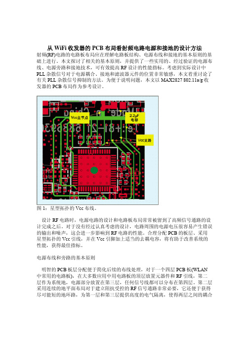
为便于说明问题,本文以MAX2827 802.11a/g收发器的PCB布局作为参考设计。
图1:星型拓扑的Vcc布线。
设计RF电路时,电源电路的设计和电路板布局常常被留到了高频信号通路的设计完成之后。
对于没有经过认真考虑的设计,电路周围的电源电压很容易产生错误的输出和噪声,这会进一步影响到RF电路的性能。
合理分配PCB的板层、采用星型拓扑的Vcc引线,并在Vcc引脚加上适当的去耦电容,将有助于改善系统的性能,获得最佳指标。
电源布线和旁路的基本原则明智的PCB板层分配便于简化后续的布线处理,对于一个四层PCB板(WLAN 中常用的电路板),在大多数应用中用电路板的顶层放置元器件和RF引线,第二层作为系统地,电源部分放置在第三层,任何信号线都可以分布在第四层。
第二层采用连续的地平面布局对于建立阻抗受控的RF信号通路非常必要,它还便于获得尽可能短的地环路,为第一层和第三层提供高度的电气隔离,使得两层之间的耦合最小。
当然,也可以采用其它板层定义的方式(特别是在电路板具有不同的层数时),但上述结构是经过验证的一个成功范例。
图2:不同频率下的电容阻抗变化。
大面积的电源层能够使Vcc布线变得轻松,但是,这种结构常常是引发系统性能恶化的导火索,在一个较大平面上把所有电源引线接在一起将无法避免引脚之间的噪声传输。
反之,如果使用星型拓扑则会减轻不同电源引脚之间的耦合。
图1给出了星型连接的Vcc布线方案,该图取自MAX2826 IEEE 802.11a/g收发器的评估板。
微波仿真论坛_141-143
Z 为阻抗;ωO 为频率;Ct 为总电容;所以可以求出:
Ct= 1.355 PF, 而: Ct = Cp + C f 。
(2)
CP 为平板电容;Cf 为筒状电容: Cp = d πD2 4S ,
C f = 2πd m ln(Rb Ra ) ,
(3) (4)
δ 为常数;S 为内导体的开路端面与外导体之间的距离;m
[3] 胡皓全,曹纪刚.新型微带交叉耦合环微波带通滤波器[J].电子科技 大学学报,2008(06):22-23.
[4] 贺瑞霞.微波技术基础[M]. 北京:人民邮电出版社,1988. [5] 程昆仑,李平辉,赵志远.一种宽阻带带通滤波器的设计方法[J].
通信技术,2011,44(03):141-142. [6] 常建刚.高性能滤波器的谐振器结构设计[J] 通信技术,2008,41
(12):300-301. [7] MAKIMOTO M,YAMSHITA S. 无线通信中的微波谐振器和滤波器原理
论[M].北京:国防工业出版社,2002.
(上接第 140 页)
Waveforms[D]. South Africa:University of Pretoria, 2005. [5] THOMAS A K, HOLGER Buchholz. STANAG 5066 – Flexible Software/
142
图 4 谐振杆剖视
图 4 通过平板和筒状电容的计算可以得其谐振频率。根
据同轴腔的谐振条件:
① å Bj = 0 ;
② jZtg(w0 L C) + 1 jw0Ct = 0 。
得出: L = C ´ tg -1 (1 Zw0 Ct ) w0 ,
(1)
微波仿真论坛_Momentum_ports_and_grounds_June2008_rev1_1
2. Executive Summary of port types available and some fundamental concepts
Demystifying ADS Momentum Ports (Juroduction
One of the most intimidating, challenging, and confusing topics to master for electromagnetic (EM) simulations is that of exciting a given design with the most accurate representation of what one would use when testing the component, module, etc. in a lab environment. Most EM tools refer to these excitations as ports. Agilent EEsof EDA’s ADS Momentum is no exception. The intent of this document is to provide a thorough reference for the various ports available in ADS Momentum and the appropriate methods to define and apply them. The authors hope that you will find this document both enlightening and a worthy resource that complements the ADS Momentum manual. Please keep in mind that this is a comprehensive document for topics related to ports, so be sure to refer to the table of contents on page 1 to see which sections are relevant to you.
微波仿真论坛_微波仿真论坛_feko5.4新例子(25,27,28,29,30)

微波仿真论坛_微波仿真论坛_feko5.4新例⼦(25,27,28,29,30)25 喇叭馈电⼤尺⼨反射镜⽤波导管端⼝激励的圆柱喇叭被⽤于激励⼀个频率为12.5Ghz的抛物⾯反射器。
反射器与喇叭天线分离很远⽽且电尺⼨很⼤(直径为36个波长)。
模型如下图25-1。
这个模型为了阐述某些feko中为了减少⼤尺⼨模型需要的资源⽽提供的技术。
图25-1圆喇叭和抛物线反射器弄清楚如何解决和近似这个问题来减少所需资源是很重要的。
某些技术可以⽤来减少资源的需求如下:●对于⼤尺度模型运⽤快速多层多极⼦(MLFMM)代替矩量法。
运⽤快速多层多极⼦能够减少相当多的内存。
(快速多层多极⼦的求解可以参照章节25.4的求解结论。
)●物理光学法(PO)可以⽤于替代计算部分模型。
⽤PO⽅法代替MOM计算将进⼀步减⼩资源的需求。
●分解问题并且运⽤等效源。
可⾏的等效源如下:—孔点源:运⽤等效原理,在区域边界上,⽤等效的电磁场源代替这个区域。
—球模式源:远场认为是外加源。
25.1 MOM喇叭和PO反射器先前的例⼦建⽴了喇叭和盘。
喇叭使⽤MOM⽅法模拟⽽盘反射器⽤PO⽅法模拟。
●freq = 12.5e9 (⼯作频率)●lam = c0/freq (⾃由空间波长)●lam_w = 0.0293 (波导波长)●h_a = 0.51*lam (波导半径)●h_b0 = 0.65*lam (椎⼝孔底半径)●h_b = lam (椎⼝孔上⽅半径)●h_l = 3.05*lam (椎⼝孔长度)●phase_centre = -2.6821e-3 (喇叭相位中⼼)●R = 18*lam (反射器半径)● F = 25*lam (反射器焦点长度)● w_l = 2*lam w (波导管长度)建⽴喇叭步骤如下:●沿z 轴建⽴cylinder ,基本中⼼为(0,0,-w_l-h_l ),半径为h_a ,⾼度为w_l ,标记为the cylinder waveguide 。
电磁场分析软件FEKO
电磁兼容分析软件FEKO (FEKO Suite 5.3)来文娟(04085065)电磁场分析软件FEKO(5.3)1. 软件背景介绍FEKO是复杂形状三维结构的电磁场分析软件,是复杂专业电磁场仿真领域中最强大的软件,应用范围非常广泛,由南非的EMSS公司开发。
FEKO基于著名的矩量法(MoM)对Maxwell方程组求解,可以解决任意复杂结构的电磁问题,是世界上第一个把多层快速多极子(MLFMM:Multi-Level Fast Multipole Method)算法推向市场的商业代码,在保持精度的前提下大大提高了计算效率,使得精确仿真电大问题成为可能(典型的如简单介质模型的RCS、天线罩、介质透镜)。
在此之前,求解此类问题只能选择高频近似方法。
FEKO中有两种高频近似技术可用,一个是物理光学(PO),另一个是一致性绕射理论(UTD)。
在MoM和MLFMM 需求的资源不够时,这两种方法提供求解的可能性。
FEKO中通过混合MoM/PO和MoM/UTD 来为电大尺寸问题的精度提供保证,非常适合于分析开域辐射、雷达散射截面(RCS)领域的各类电磁场问题。
FEKO还针对许多特定问题,例如平面多层介质结构、金属表面的涂覆等等,开发了量身定制的代码,在保证精度的同时获得最佳的效率。
2. 主要功能1.电大问题的求解:FEKO通过MLFMM、MoM/PO、MoM/UTD从算法上提供了电大问题求解的途径;2.丰富的求解器选择:FEKO提供多种核心算法,矩量法(MoM)、多层快速多极子方法(MLFMM)、物理光学法(PO)、一致性绕射理论(UTD)、有限元(FEM)、平面多层介质的格林函数,以及它们的混合算法来高效处理各类不同的问题;3.优化功能:FEKO提供了离散点计算方法、单纯形方法、共轭梯度法、准牛顿法等多种优化方法;4.快速宽频响应计算:FEKO通过自适应频率点采样和插值,提供宽频率响应的快速计算能力;5.时域求解:FEKO基于频域分析,同时通过FFT提供时域响应分析能力;6.强大的前后处理功能:CADFEKO提供直接面向求解器的3D图形建模和网格划分功能,支持多种CAD格式的网格文件导入:包括FEMAP Neutral (*.neu),AUTOCAD (*.dxf),特定的ASCII,NASTRAN (*.nas),STL(*.stl),ANSYS (*.cdb),ParaSolid等等;POSTFEKO提供图形化后处理能力。
微波仿真论坛_CST MWS 2
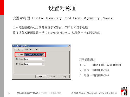
启动优化器
启动优化器(Solve->Transient Solver->Opitimization)
启动优化器
优化器窗口
78
2004.09.28 CST MWS用户讲座 上海微系统所
© CST China - Shanghai -
优化器设定-优化参数
选中优化器的优化参数页(Parameters)
Farfield-特性参数(2)
在Farfield Plot中选择General页,在绘图类型(Plot type)中选择Polar 并设置好绘图平面参数并确定,就可得到对应的极坐标方向图
绘图类型
绘图平面
Theta=90°
绘图步长 (决定图线的光滑度)
Phi=90°
68 2004.09.28 CST MWS用户讲座 上海微系统所
选中offset变量,在Reset min/max框中输入20,并点击此按钮 统一设定参数 变化范围
毋需优化参数 需优化参数 最大/最小值 初始值 当前值 最佳值
79
2004.09.28 CST MWS用户讲座 上海微系统所
© CST China - Shanghai -
天线方向图 (与模型朝向一致)
Farfield
66
2004.09.28 CST MWS用户讲座 上海微系统所
方向性系数 辐射效率 等相关信息 China - Shanghai © CST
Farfield-特性参数(1)
可在“特性参数”窗口对Farfield结果的显示进行设置
82 2004.09.28 CST MWS用户讲座 上海微系统所 © CST China - Shanghai -
开始优化
开始优化时,系统会自动切换到信息页(Info),显示优化进程中各种信息 其中有迭代次数,优化目标函数初始值,上次值和最佳值 其中“最优参数值”(Best parameters so far),显示了当前的最优参数
微波仿真论坛_Silicon_sch_spice_models
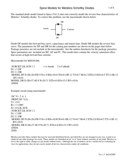
1 of 6Spice Models for Metelics Schottky DiodesThe standard diode model found in Spice (Ver 2) does not correctly model the reverse bias characteristics of Metelics’ Schottky diodes. To correct this problem, use the macromodel shown below.Diode DF models the forward bias curve, capacitance and transit time. Diode DR models the reverse bias curve. The parameters for DF and DR for the catalog part numbers are shown on the pages that follow. Package parasitics are not include in the macromodel. See the outline datasheets for the package parasitics. Spice parameters not included are KF, AF and FC. This model does contain the velocity saturation effect that occurs at high forward bias currents.Macromodel for MSS30,046.SUBCKT LB_SCH 1 2 1 is Anode 2 is Cathode D1 1 2 DF D2 2 1 DR.MODEL DF D (IS=26.05E-9 N=1.0 RS=10.0 CJO=0.10E-12 VJ=0.7 M=0.2 XTI=2.0 EG=0.5 TT=3.0E-12 BV=10.0)MODEL DR D (IS=37.4E-9 N=20.71 XTI=4.0 EG=33.5 BV=10.0) .ENDSExample circuit using macromodel.DC V1 .2 .6 .1 .PRINT DC V(2) V1 1 0 0 R1 1 2 1000 X1 2 0 LB_SCH.SUBCKT LB_SCH 1 2 D1 1 2 DF D2 2 1 DR.MODEL DF D (IS=26.05E-9 N=1.0 RS=10.0CJO=0.10E-12 VJ=0.7 M=0.2 XTI=2.0 EG=0.5 TT=3.0E-12 BV=10.0).MODEL DR D (IS=37.4E-9 N=20.71 XTI=4.0 EG=33.5 BV=10.0) .ENDS.ENDAnodeCathodeDFMetelics provides Spice models that may be used and distributed freely, provided they are not changed in any way, resold or in-cluded in any other package for resale. These models are furnished on an "as is" basis without warranty of any kind. Metelics re-serves the right to make changes to any model without notice. Although the use of models can be a useful tool in evaluating de-vices for applications, they do not exactly model all device characteristics under all conditions.2 of 6Part Number IS RSohms CJO pFMSS25,047MSS25,14320.0E-9 to 1.0E-6 25 to 60 0.07 to 0.10MSS25,049MSS25,14520.0E-9 to 1.0E-6 25 to 47 0.09 to 0.12 MSS25,141 20.0E-9 to 1.0E-6 25 to 60 0.05 to 0.08 N=0.92 to 1.0VJ=0.7M=0.2TT=3.0E-12EG=0.22XTI=9.5BV=20.0Parameters for diode DRIS=680.0E-9N=51.0XTI=2.0EG=20BV=20.0CJ0=0.0RS=0.0Parameters for diode DFSpice Model Parameters for MSS25,000 Series Diodes Spice Model Parameters for MSS30,000 Series DiodesPart Number IS RSohms CJO pFMSS30,046MSS30,142MSS30,242MSS30,346MSS30,442MSS30,B46MSS30,PCR46MSS30,CR469.1nA to 43nA 8 to 12 0.08 to 0.12MSS30,050MSS33,148MSS30,248MSS30,44816.5nA to 80nA 4.8 to 7.2 0.12 to 0.17MSS30,154 MSS30,254 MSS30,454 MSS30,B53 MSS30,PCR53 MSS30,CR53 43nA to 154nA 2.4 to 3.6 0.17 to 0.27N=1.0VJ=0.7M=0.2TT=3.0E-12EG=0.5XTI=2.0BV=10.0Parameters for diode DRIS=37.4nAN=20.71XTI=4.0EG=33.5BV=10.0Parameters for diode DF3 of 6Spice Model Parameters for MSS39,000 Series DiodesPartNumberIS N XTI EGMSS39,045MSS39,04834.8nA 33.96 4.0 10.0MSS39,144 MSS39,146 MSS39,148 MSS39,152 35.9nA 23.93 4.0 10.0BV10.010.0Parameters for diode DR4 of 6 Spice Model Parameters for MSS40,000 Series DiodesParameters for diode DFPart Number IS RSohms CJO pFMSS40,045MSS40,3413nA to 4.5pA 5.6 to 8.4 0.07 to 0.11MSS40,048MSS40,148MSS40,248MSS40,4485.5nA to 11pA 5.6 to 8.4 0.09 to 0.14MSS40,141MSS40,2443.5nA to4.9pA 8 to 12 0.05 to 0.07MSS40,155MSS40,255MSS40,4559.5nA to 26.5pA 4 to 6 0.2 to 0.3MSS40,B46MSS40,CR46MSS40,PCR460.7pA to 1nA 8 to 20 0.07 to 0.125MSS40,B53 MSS40,CR53 MSS40,PCR53 3.2pA to 2.5nA 5 to 10 0.1 to 0.25N=1.0VJ=0.7M=0.2TT=3.0E-12EG=0.6XTI=2.0BV=10.0Parameters for diode DRIS=37.4nAN=20.71XTI=4.0EG=9.0BV=10.0Parameters for diode DFPart Number IS RSohms CJO pFMSS50,048 250pA to 110fA 5.6 to 8.4 0.09 to 0.14 MSS50,062 205pA to 90fA 1.6 to 2.4 0.4 to 0.6 MSS50,146 146pA to 47fA 7.2 to 10.8 0.05 to 0.09 MSS50,244,341,448 146pA to 47fA 5.8 to 7.2 0.16 to 0.24 MSS50,B46,CR46,PCR46 130pA to 115fA 8 to 15 0.07 to 0.125 MSS50,B53,CR53,PCR53 250pA to 110fA 5 to 10 0.1 to 0.25 N=1.0VJ=0.7M=0.2TT=3.0E-12 EG=0.76 XTI=2.0 BV=10.0Part Number IS N XTI EG MSS50,048 35.9nA 23.93 4.0 8.0 MSS50,062,146,244,341,448 34.8nA 33.96 4.0 8.0 MSS50,B46,CR46,PCR46 37.4nA 20.71 4.0 8.0BV 10.0 10.0 10.0Parameters for diode DR5 of6 Spice Model Parameters for MSS60,000 Series DiodesParameters for diode DFPart Number IS RSohms CJO pFMSS60,144MSS60,244MSS60,444MSS60,341319fA to 8.3fA 10 to 20 0.06 to 0.1MSS60,148MSS60,248MSS60,448265fA to 6.8fA 7 to 13 0.09 to 0.15MSS60,153MSS60,253MSS60,453220fA to 5.6fA 3 to 7 0.15 to 0.25MSS60,B46 2.2pA to 0.07fA 10 to 20 0.06 to 0.125 MSS60,B53 5pA to 0.3fA 7 to 13 0.1 to 0.25 MSS60,CR46,PCR46 9pA to 0.6fA 10 to 20 0.06 to 0.125 MSS60,CR53,PCR53 13pA to 1.2fA 7 to 13 0.1 to 0.25 N=1.0VJ=0.7M=0.2TT=3.0E-12EG=0.88XTI=2.0BV=10.0Parameters for diode DRIS=35.9nAN=23.93XTI=4.0EG=7.0BV=10.0Suface Mount SchottkysPart Number Spice Model SMST3012 MSS30,050 SMST4012 MSS40,048 SMST6012 MSS60,148 SMST3004SMST4004SMST6004SMSD3012 MSS30,050 SMSD4012 MSS40,048 SMSD6012 MSS60,1486 of 6Schottky Diode ConfigurationsSingleAnti Parallel PairSeries TeeRing Quad - four junctionBridge Quad - four junctionRing Quad - eight junctionCrossover RingCrossover Bridge。
微波仿真论坛_应用Designer和HFSS对微波滤波器的协同仿真

7
些模型导入电路模块中 。在电路形式下 ,每个部分 被抽象成一个多端口器件 ,将这些多端口器件按逻 辑关系联结起来组成一个电路模型 ,这些电磁结构 模型被导入到电路模块中 ,它们仍保持其独立性 。 这样划分的理由是谐振杆处场的分布是对称的 ,切 面是理想电壁对称面 ,划分并不改变场的分布 ,对称 面的应用加快了求解速度 。图 4 为划分结构示意图 和电路端口连接模型 。
图 6 三种结构电路仿真结果
虽然都可得到近似的结果 ,但其中的原理有区 别 ,也说明了划分面选取的重要性 。
场模型中激励端口的模式数对应于电路模型中 的端口网络节点 ,为求解的准确 ,可增加设置模式 数 。对于波导和给定横截面的传输线 ,存在给定频 率下的一系列基本场模式 ,在波导中 ,场是这些模式 的线性组合 。仿真分析时不可能考虑所有的模式 , 而必须在一定的模式数处将场的级数求和式加以截 断 。由一个给定模式激励信号产生的场包含因结构 的不连续性而产生的高阶模式的反射 。这些高阶模 式被反射回激励端口或传输到另一端口 ,计算 S 参 数时必须考虑到这些模式 。所取模式数目的不同 , 求取精度就不同 。模式数太多 ,计算时间会增加 ,求 解精度不会显著提高 ,只需计算结果收敛即可 。
传统的等效电路法将复杂的场问题近似为一些简化 的级联公式可类似推导 。
的等效电路模型 ,其具有简单易行的特点 ,精度依赖
feko仿真原理与工程应用

feko仿真原理与工程应用1. 引言feko是一种用于高频电磁场仿真的软件工具,具有广泛的工程应用。
本文将介绍feko的仿真原理以及其在工程应用中的具体应用案例。
2. feko的仿真原理feko采用了计算电动力学(CED)方法进行电磁场仿真。
CED方法是一种基于边界元素法(BEM)的数值计算方法,它通过将物体表面离散化为许多小面元,在每个小面元上求解边界电磁问题,最终得到整个电磁场的分布。
feko的仿真原理可以分为以下几个步骤:1.几何建模:用户需要将待仿真的物体几何模型导入feko中,可以直接导入常见的几何文件格式,如STL、STEP等。
2.离散化:feko会将导入的几何模型进行离散化处理,将物体表面离散化为小面元,并为每个小面元分配适当的边界条件。
3.边界元素法:在每个小面元上,feko通过求解边界电磁问题得到该小面元上的电磁场分布。
边界条件可以根据具体情况设定,如电导率、介电常数等。
4.全局问题:考虑到解的连续性,feko会根据边界元素法得到的电磁场分布,进一步求解整个电磁场的分布,包括物体内部和周围的电磁场。
5.结果输出:feko可以输出仿真结果的各种参数,如电磁场强度、电场分布、磁场分布等。
3. feko的工程应用feko在工程领域有着广泛的应用,主要涵盖以下几个方面:3.1 电磁兼容性(EMC)设计电磁兼容性设计是为了保证各种电子设备在电磁环境中正常工作而进行的设计。
feko可以对设备进行电磁辐射和敏感性分析,通过优化设备结构和地线设计,提高设备的电磁兼容性。
3.2 天线设计天线设计是feko的主要应用领域之一。
feko可以对天线进行性能分析,包括辐射模式、增益、方向性等。
通过对天线的优化设计,可以提高天线的性能和信号接收质量。
3.3 毫米波通信系统设计毫米波通信是一种新型的高速无线通信技术。
feko可以对毫米波通信系统进行仿真分析,包括传输损耗、发射功率控制、信号干扰等。
通过优化设计,可以提高毫米波通信系统的性能和可靠性。
微波仿真论坛_5.4新特性

F E K O S u i t e5.4新版本说明July 2008 (Changes since Suite 5.3)翻译:Aug., 2008 安世亚太F E K O S u i t e5.4在5.3的基础上有了很大的改进和扩展。
最关键的是提供了更为完善的F E K O求解器特性设置的图形化界面操作集成,以及解除了许多不同求解方法之间的条件限制(包括优化算法本身),还有加入一些其他求解方法(比如周期性边界条件)。
您可能需要一个新的支持5.4版本的l i c e n s e来激活这个版本。
这个许可文件同时也支持其他所有高于3.1.2的F E K O版本,或许由于某种不可预期的原因可能需要用到早期的版本。
最重要的新特性列举如下。
除列出来的项目之外,新版本还包括很多小的b u g修复和附加功能的添加。
用户界面(U s e r i n t e r f a c e)1.在C A D F E K O中,提供了建立几何模型的可替代的其他方式,比如,提供通过不同的参数序列来建立几何原型,定义对话框中的示意图也得到了改进以便更方便的创建模型。
2.在C A D F E K O中,可以直接建立抛物线和双曲线几何模型。
3.在C A D F E K O中,加入了一个新的高级拉伸建模工具,补充现有的拉伸建模方式,允许绕着固定的路径拉伸面和线。
被拉伸物最后可以保留,可以平行于原来的朝向或者相对于拉伸路径的朝向。
变换过程中可以加入缩放和旋转。
(比如,被拉伸建模的部分可以沿着拉伸的方向放大或缩小,还可以旋转。
)4.新添一个面缝合工具,可以将两个本来存在缝隙的边缝合在一起,实现模型修补,这在很多导入模型中是非常有用的。
(5.3版的C A D F E K O补丁已经具备这个功能)5.C A D F E K O中新增导入D X F C A D几何模型的模块。
导入模块允许D X F C A D模型直接导入成C A D F E K O中的部件,同时也可以导入D X F的网格。
微波仿真论坛_微波实验室中的线性仿真
微波实验室中的线性仿真线性仿真器是利用节点分析法来仿真电路特性的。
线性仿真被用在低噪声放大器、滤波器和输入矩阵特性的耦合器中。
线性仿真器能算出的测量值有:输出值、噪声系数、反射系数和噪声环。
如何创建集总滤波器这个例子教会我们在微波实验室中如何利用线性仿真器来仿真基本的集总滤波器。
一般包含一下步骤:●创建电路图●添加曲线图和测量值●分析电路●调整电路●创建变量●最优化电路创建电路图创建一个项目:选择File > New Project ;选择File > Save Project As,弹出另存为对话框;命名项目的文件名(如"linear_example"),然后点击Save。
设置缺省的项目单位选择Options > Project Options,打开项目选项对话框;点击Global Units项目栏;点击右边的箭头找到你所要的单位,然后点击OK。
创建电路图选择Project > Add Schematic > New Schematic。
弹出Create New Schematic对话框;输入文件名"lpf",然后点击OK。
在活动区域电路图纸被打开,在项目浏览器中Circuit Schematics下方多出一个Schematic文件。
在电路图中放置元件在电路图窗口的右上方通过滑动箭头来查看你所需要的电路部分元件。
先在环境浏览窗口点击窗口左下方的Elem栏;在环境浏览窗口中点击图标左边的+号弹出Lumped Element子菜单;单击Lumped Element下的Inductor,在下面的窗口显示一组inductor模块;单击模块,把它放置到电路图中;按照图示的位置放好,然后单击鼠标放置提示:在电路图中连接两个元件的捷径是把两个元件的节点放在一起会自动连接。
当连接后,节点会显示蓝色小方块。
如果你第一次没有连接好,只要单击元件图标,按下鼠标拖动元件到适当的位置就可以了。
微波仿真论坛_matlab feko

Matlab 与Feko软件混合目录•概述•模型的建立•EditFeko中控制卡的编辑•Matlab调用Feko 讨论•Matlab对Feko结果文件的处理Matlab调用Feko的几个要点•Matlab调用Feko的几个要点–在Matlab以如下形式调用Fekodos('prefeko OnespiralAnt');dos (‘runfeko OnespiralAnt');其中的OnespiralAnt为Feko工程文件的名称,prefeko和runfeko是Feko关键字符串,分别表示Feko预处理和Feko求解器–在Feko中生成的.pre和.out可以以文本的形式打开,所以在Mablab中可以象处理文本那样来处理这些文件:在Matlab定义一个变量,该变量对应于Feko的.pre文件中某一个变量(如:工作频率、几何模型的尺寸变量、模型旋转角等),这样,就可以用Matlab控制Feko中的这个变量,每改变一次该变量的值就可以重新生成一个新的.pre文件,然后调用runFeko运行新生成的.pre文件;同样,可以应用Matlab像处理文本一样来处理Feko的结果文件.out,来对仿真结果进行处理。
–Matlab生成的.m文件需要和Feko的工程文件、.pre文件及输出文件存放在同一文件夹中。
举例(单螺旋天线)•问题描述–以单螺旋为例来说明如何用Matlab控制Feko•可以在CadFeko中进行建模;•也可以在EditFeko中进行建模;(有些问题用EditFeko处理会非常方便)–Matlab可以控制Feko脚本文件.pre中的某个或某几个变量,在该例子中是控制螺旋天线的旋转角度#alpha–Matlab控制Feko的结果文件(.out),(要想很好的处理结果文件,必须对其格式非常清楚)读取内部的源阻抗数值目录•概述•模型的建立•EditFeko中控制卡的编辑•Matlab调用Feko 讨论•Matlab对Feko结果文件的处理螺旋天线的建立(CadFeko)•建立Feko工程文件“OneSpiralAnt”•双击Variables添加以下变量:freq=3.0e+10n=6.5, lambda=c0/freqD=lambda/pi,s=0.225*lambda,seg_len=lambda/15seg_rad=lambda/200tri_len=lambda/20.0a=0.75*lambda•点击图标添加螺旋曲线helix•点击图标把helix模型分成两部分选择小的一部分更名为:feed模型建立•点击图标创建地板ground网格剖分•选中所有模型点击图标进行模型合并,并把新生成的模型更名为spiral •把馈源位置的线元更名为feed•点击菜单“Mesh\create mesh”或按住键盘Ctrl+M进行网格剖分目录•概述•模型的建立•EditFeko中控制卡的编辑•Matlab调用Feko 讨论•Matlab对Feko结果文件的处理EditFeko处理•按住Alt+2进行预处理,并保存工程文件•按住Alt+1调出EditFeko•在IN卡下边添加FM卡•在FM卡下边添加“#alpha=0”•然后添加TG卡** TG卡用来控制模型的平移与旋转,在该项目中,我们是把该基本模型沿y轴旋转#alpha角度,初始值是0度•修正FR卡•添加A1卡•添加FF卡•所有的控制卡添加完毕后保存该文件Spiral.feed目录•概述•模型的建立•EditFeko中控制卡的编辑•Matlab调用Feko 讨论•Matlab对Feko结果文件的处理Matlab部分处理•点击Matlab程序中的M-file editor或先进入Matlab主程序,在主程序中点击菜单“File\New\M file”进行.m文件的制作部分(可以命名为OneSpiralAnt.m)•第一步添加如下命令clear all; %清除工作间的变量和函数•第二步添加循环(该循环的目的是为了得到不同的旋转角alpha,循环变量用i表示,i的变化范围是从1到5,步长为1,alpha表示为10*i)for i=1:1:5第一部分:初始化变量部分;第二部分:文件的读写部分;第三部分:生成新的脚本文件;第四部分:Matlab中调用Feko;end % 结束for循环•第一部分:变量的初始化special_str_1='prefeko ';special_str_2='runfeko ';project_name=' OneSpiralAnt_';prestr='#alpha='; % Initialise a variable for special string注释:变量special_str_1、special_str_2和project_name是为了最终装配最终的字符串形式“runfeko OneSpiralAnt_1.pre”而设定的,因为在循环中,我们是以OneSpiralAnt_1.pre、OneSpiralAnt_2.pre…OneSpiralAnt_5.pre的形式来存储脚本文件的,而且每循环生成一个.pre脚本文件,我们会运行一次Feko软件,这样处理就相对比较灵活了prestr变量是一个关键字符,用于存储模型的旋转角度•第二部分:文件的读写部分fid_r=fopen(‘OneSpiralAnt.pre’,‘r’); % Define a file reading point (定义读文件指针)fid_w=fopen(‘OneSpiralAnt.tmp’,‘w’); %Define a file writting point (定义写文件指针)while ~feof(fid_r) % while not the end of the file (如果不是文件的结尾就继续循环)line_r=fgetl(fid_r); % get each line value (遍历每一行的值)g=strfind(line_r,‘#alpha=’); % whether this line need be modified(是否是需要修改的那一行)if g>0 %如果是需要修改的那一行,则在if…end区间修改这一行的值newvalue=num2str(10*(i-1));line_r=strcat(prestr,newvalue); % modify this line's value, line_r=‘#alpha=10’or 20…end% 通过fprintf语句把line_r的值写入fid_w指向的文件OneSpiralAnt.tmp中fprintf(fid_w,'%s\n',line_r); % write each line to the file 'OneSpiralAnt.tmp' end %end while (结束读写脚本文件循环)fclose(fid_r); % close file reading point (关闭读文件指针)fclose(fid_w); % close file writting point (关闭写文件指针)•第三部分:生成新的脚本文件% get and save each .pre file in the form of OneSpiralAnt_1.pre,OneSpiralAnt_2.pre...% 我们需要生成的文件的名称分别为OneSpiralAnt_1.pre,OneSpiralAnt_2.pre,OneSpiralAnt_3.pre, % OneSpiralAnt_4.pre以及OneSpiralAnt_5.pre% new_file_name分别为OneSpiralAnt_1.pre, OneSpiralAnt_2.pre, OneSpiralAnt_3.pre…new_file_name=strcat('OneSpiralAnt_',num2str(i));new_file_name=strcat(new_file_name,'.pre');% 把文件OneSpiralAnt.tmp中的内容拷贝到new_file_name中,即生成上边提到的5个.pre文件中copyfile('OneSpiralAnt.tmp',new_file_name);•第四部分:Matlab调用Feko% Assemble the “prefeko OneSpiralAnt_i.pre”stringsspecial_str_1=strcat(special_str_1,project_name);special_str_1=strcat(special_str_1,num2str(i));special_str_1=strcat(special_str_1,'.pre');% Assemble the “runfeko OneSpiralAnt_i.pre”stringsspecial_str_2=strcat(special_str_2,project_name);special_str_2=strcat(special_str_2,num2str(i));special_str_2=strcat(special_str_2,'.pre');%invoke feko functions (通过dos函数调用prefeko、funfeko)dos(special_str_1); % dos(‘prefeko OneSpiralAnt_1.pre')dos(special_str_2); % dos('runfeko OneSpiralAnt_1.pre')%;完整的Matlab代码结果文件分析•打开Matlab 主程序,调出OneSpiralAnt.m 文件,然后点击菜单Debug\Run 或直接按F5开始运行,运行完毕后,•我们就得到了5个后缀为.pre 的脚本文件,5个PostFeko 文件(后缀为.bof,.fek )以及5个后缀为.out 的结果文件,它们分别对应不同的角度alpha ,分别打开*_1.fek, *._2.fek, *_3.fek,*_4.fek 和*_5.fek 可以看到模型随角度的变化alpha=0alpha=10alpha=20alpha=30alpha=40EditFeko文件中alpha 角度的变化alpha=0alpha=40 alpha=10alpha=20alpha=30目录•概述•模型的建立•EditFeko中控制卡的编辑•Matlab调用Feko 讨论•Matlab对Feko结果文件的处理•借用前边的项目文件OneSpiralAnt.cfx,OneSpiralAnt.cfm和OneSpiralAnt.pre。
- 1、下载文档前请自行甄别文档内容的完整性,平台不提供额外的编辑、内容补充、找答案等附加服务。
- 2、"仅部分预览"的文档,不可在线预览部分如存在完整性等问题,可反馈申请退款(可完整预览的文档不适用该条件!)。
- 3、如文档侵犯您的权益,请联系客服反馈,我们会尽快为您处理(人工客服工作时间:9:00-18:30)。
Matlab 与Feko软件混合目录•概述•模型的建立•EditFeko中控制卡的编辑•Matlab调用Feko 讨论•Matlab对Feko结果文件的处理Matlab调用Feko的几个要点•Matlab调用Feko的几个要点–在Matlab以如下形式调用Fekodos('prefeko OnespiralAnt');dos (‘runfeko OnespiralAnt');其中的OnespiralAnt为Feko工程文件的名称,prefeko和runfeko是Feko关键字符串,分别表示Feko预处理和Feko求解器–在Feko中生成的.pre和.out可以以文本的形式打开,所以在Mablab中可以象处理文本那样来处理这些文件:在Matlab定义一个变量,该变量对应于Feko的.pre文件中某一个变量(如:工作频率、几何模型的尺寸变量、模型旋转角等),这样,就可以用Matlab控制Feko中的这个变量,每改变一次该变量的值就可以重新生成一个新的.pre文件,然后调用runFeko运行新生成的.pre文件;同样,可以应用Matlab像处理文本一样来处理Feko的结果文件.out,来对仿真结果进行处理。
–Matlab生成的.m文件需要和Feko的工程文件、.pre文件及输出文件存放在同一文件夹中。
举例(单螺旋天线)•问题描述–以单螺旋为例来说明如何用Matlab控制Feko•可以在CadFeko中进行建模;•也可以在EditFeko中进行建模;(有些问题用EditFeko处理会非常方便)–Matlab可以控制Feko脚本文件.pre中的某个或某几个变量,在该例子中是控制螺旋天线的旋转角度#alpha–Matlab控制Feko的结果文件(.out),(要想很好的处理结果文件,必须对其格式非常清楚)读取内部的源阻抗数值目录•概述•模型的建立•EditFeko中控制卡的编辑•Matlab调用Feko 讨论•Matlab对Feko结果文件的处理螺旋天线的建立(CadFeko)•建立Feko工程文件“OneSpiralAnt”•双击Variables添加以下变量:freq=3.0e+10n=6.5, lambda=c0/freqD=lambda/pi,s=0.225*lambda,seg_len=lambda/15seg_rad=lambda/200tri_len=lambda/20.0a=0.75*lambda•点击图标添加螺旋曲线helix•点击图标把helix模型分成两部分选择小的一部分更名为:feed模型建立•点击图标创建地板ground网格剖分•选中所有模型点击图标进行模型合并,并把新生成的模型更名为spiral •把馈源位置的线元更名为feed•点击菜单“Mesh\create mesh”或按住键盘Ctrl+M进行网格剖分目录•概述•模型的建立•EditFeko中控制卡的编辑•Matlab调用Feko 讨论•Matlab对Feko结果文件的处理EditFeko处理•按住Alt+2进行预处理,并保存工程文件•按住Alt+1调出EditFeko•在IN卡下边添加FM卡•在FM卡下边添加“#alpha=0”•然后添加TG卡** TG卡用来控制模型的平移与旋转,在该项目中,我们是把该基本模型沿y轴旋转#alpha角度,初始值是0度•修正FR卡•添加A1卡•添加FF卡•所有的控制卡添加完毕后保存该文件Spiral.feed目录•概述•模型的建立•EditFeko中控制卡的编辑•Matlab调用Feko 讨论•Matlab对Feko结果文件的处理Matlab部分处理•点击Matlab程序中的M-file editor或先进入Matlab主程序,在主程序中点击菜单“File\New\M file”进行.m文件的制作部分(可以命名为OneSpiralAnt.m)•第一步添加如下命令clear all; %清除工作间的变量和函数•第二步添加循环(该循环的目的是为了得到不同的旋转角alpha,循环变量用i表示,i的变化范围是从1到5,步长为1,alpha表示为10*i)for i=1:1:5第一部分:初始化变量部分;第二部分:文件的读写部分;第三部分:生成新的脚本文件;第四部分:Matlab中调用Feko;end % 结束for循环•第一部分:变量的初始化special_str_1='prefeko ';special_str_2='runfeko ';project_name=' OneSpiralAnt_';prestr='#alpha='; % Initialise a variable for special string注释:变量special_str_1、special_str_2和project_name是为了最终装配最终的字符串形式“runfeko OneSpiralAnt_1.pre”而设定的,因为在循环中,我们是以OneSpiralAnt_1.pre、OneSpiralAnt_2.pre…OneSpiralAnt_5.pre的形式来存储脚本文件的,而且每循环生成一个.pre脚本文件,我们会运行一次Feko软件,这样处理就相对比较灵活了prestr变量是一个关键字符,用于存储模型的旋转角度•第二部分:文件的读写部分fid_r=fopen(‘OneSpiralAnt.pre’,‘r’); % Define a file reading point (定义读文件指针)fid_w=fopen(‘OneSpiralAnt.tmp’,‘w’); %Define a file writting point (定义写文件指针)while ~feof(fid_r) % while not the end of the file (如果不是文件的结尾就继续循环)line_r=fgetl(fid_r); % get each line value (遍历每一行的值)g=strfind(line_r,‘#alpha=’); % whether this line need be modified(是否是需要修改的那一行)if g>0 %如果是需要修改的那一行,则在if…end区间修改这一行的值newvalue=num2str(10*(i-1));line_r=strcat(prestr,newvalue); % modify this line's value, line_r=‘#alpha=10’or 20…end% 通过fprintf语句把line_r的值写入fid_w指向的文件OneSpiralAnt.tmp中fprintf(fid_w,'%s\n',line_r); % write each line to the file 'OneSpiralAnt.tmp' end %end while (结束读写脚本文件循环)fclose(fid_r); % close file reading point (关闭读文件指针)fclose(fid_w); % close file writting point (关闭写文件指针)•第三部分:生成新的脚本文件% get and save each .pre file in the form of OneSpiralAnt_1.pre,OneSpiralAnt_2.pre...% 我们需要生成的文件的名称分别为OneSpiralAnt_1.pre,OneSpiralAnt_2.pre,OneSpiralAnt_3.pre, % OneSpiralAnt_4.pre以及OneSpiralAnt_5.pre% new_file_name分别为OneSpiralAnt_1.pre, OneSpiralAnt_2.pre, OneSpiralAnt_3.pre…new_file_name=strcat('OneSpiralAnt_',num2str(i));new_file_name=strcat(new_file_name,'.pre');% 把文件OneSpiralAnt.tmp中的内容拷贝到new_file_name中,即生成上边提到的5个.pre文件中copyfile('OneSpiralAnt.tmp',new_file_name);•第四部分:Matlab调用Feko% Assemble the “prefeko OneSpiralAnt_i.pre”stringsspecial_str_1=strcat(special_str_1,project_name);special_str_1=strcat(special_str_1,num2str(i));special_str_1=strcat(special_str_1,'.pre');% Assemble the “runfeko OneSpiralAnt_i.pre”stringsspecial_str_2=strcat(special_str_2,project_name);special_str_2=strcat(special_str_2,num2str(i));special_str_2=strcat(special_str_2,'.pre');%invoke feko functions (通过dos函数调用prefeko、funfeko)dos(special_str_1); % dos(‘prefeko OneSpiralAnt_1.pre')dos(special_str_2); % dos('runfeko OneSpiralAnt_1.pre')%;完整的Matlab代码结果文件分析•打开Matlab 主程序,调出OneSpiralAnt.m 文件,然后点击菜单Debug\Run 或直接按F5开始运行,运行完毕后,•我们就得到了5个后缀为.pre 的脚本文件,5个PostFeko 文件(后缀为.bof,.fek )以及5个后缀为.out 的结果文件,它们分别对应不同的角度alpha ,分别打开*_1.fek, *._2.fek, *_3.fek,*_4.fek 和*_5.fek 可以看到模型随角度的变化alpha=0alpha=10alpha=20alpha=30alpha=40EditFeko文件中alpha 角度的变化alpha=0alpha=40 alpha=10alpha=20alpha=30目录•概述•模型的建立•EditFeko中控制卡的编辑•Matlab调用Feko 讨论•Matlab对Feko结果文件的处理•借用前边的项目文件OneSpiralAnt.cfx,OneSpiralAnt.cfm和OneSpiralAnt.pre。