单片机毕业设计外文翻译3
plc单片机 毕业论文文献翻译 中英文对照

外文翻译:The monolithic In order to prevent without authorization the visit or the copy monolithic integrated circuit machine in the procedure, the majority of monolithic integrated circuits all has the encryption to lock the localization or the encryption byte, by protects the internal procedure. If in programming time encrypts locks the localization to enable (locking), is unable with the ordinary programming directly reading in the monolithic integrated circuit the procedure, this is the so-called copy protection or says the fixed function. In fact, such protective measures are very frail, is very easily explained. The monolithic integrated circuit aggressor with the aid of the special purpose equipment or the self-made equipment, using the monolithic integrated circuit chip design in loophole or the software flaw, through the many kinds of technical method, may withdraw the essential information from the chip, gains in the monolithic integrated circuit the procedure. Therefore, has the newest technology extremely as electronic products project engineer which the essential understanding current monolithic integrated circuit attacks, achieves knows oneself and the other side, knows fairly well, can effectively prevent oneself spends the product which the massive moneys and the time laboriously designs the matter occurrence which is counterfeited by a others night between.monolithic integrated circuits attacks technology:At present, attacks the monolithic integrated circuit mainly to have four kind of technologies, respectively is:This technical usual use processor correspondence connection and in the use agreement, the encryption algorithm or these algorithm security loophole carries on the attack. The software attack obtains the success a case in point is to early A T M E L A the T 89 C series monolithic integrated circuit attack. The aggressor has used in this series monolithic integrated circuit cleaning operation succession design loophole, uses from arranges the procedure to lock the localization after the cleaning encryption, stops the next step of cleaning internal program memory data the operation, thus makes to add the dense monolithic integrated circuit not to turn the encryption monolithic integrated circuit, then use programming read-out internal procedure.This technology usually monitors the processor by the high time resolution when the normal operation all power sources and the connection connection simulation characteristic, and through monitors its electromagnetic radiation characteristic to implement the attack. Because the monolithic integrated circuit is an active electronic device, when it carries out the different instruction, the corresponding mains input consumption also correspondingly changes. Like this analyzes and examines these changes through the use special electronic surveying instrument and mathematics statistical method, then gains in the monolithic integrated circuit the specific essential information.the mistake has the technology This technical use exceptionally working condition causes the processor to make a mistake, then provides the extra visit to carry on the attack. Uses the most widespread mistake to have the attack method including the voltage impact and the clock impact. The low voltage and the high voltage attack may usefor to forbid the protection circuit work or to fortected the information. The power source and the clock transient state jump may affect the single scroll instruction in certain processors the decoding and the ece the processor to carry out the misoperation. Perhaps the clock transient state jump can reposition the protection circuit but not to be able to destroy is proxecution.This technology is the direct exposed chip interior segment, then the observation, holds controls, disturbs the monolithic integrated circuit by to achieve the attack goal.In order to facilitate in order to, the people divide into above four kind of attacks technology two kinds, a kind is the invasion attack (physical attack), this kind of attack needs to destroy the seal, then with the aid of the semiconductor test facility, the microscope and the micro locator, several hours even several week time can complete on the special laboratory flower. All micro probes technology all belongs to the invasion attack. Moreover three methods belong to the non- invasion attack, the monolithic integrated circuit which attacks cannot by the physical damage. In certain situation non- invasion attacks is specially dangerous, this is because the non- invasion attack needs the equipment usually to be possible the self-restraint and the promotion, therefore is extremely inexpensive.The majority of non- invasions attack needs the aggressor to have the good processor knowledge and the software knowledge. Is opposite with it, the invasion probe attack then does not need too many initial knowledge,moreover usually may use the one whole set similar technology to cope with the width scope the product. Therefore, the attack often starts to the monolithic integrated circuit from the invasion reverse engineering, the accumulation experience is helpful to the development more inexpensive and the fast non- invasion attack technology.Last step will be seeks the protection melt silk the position and protects the melt silk to expose under the ultraviolet ray. With enlargement factor at least 100 time of microscopes, inputs the foot from the programming voltage the segment to track generally, seeks the protection melt silk.This technical use exceptionally working condition causes the processor to make a mistake, then provides the extra visit to carry on the attack. Uses the most widespread mistake to have the attack method including the voltage impact and the clock impact. The low voltage and the high voltage attack may use for to forbid the protection circuit work or to force the processor to carry out the misoperation. Perhaps the clock transient state jump can reposition the protection circuit but not to be able to destroy is protected the information. The power source and the clock transient state jump may affect the single scroll instruction in certain processors the decoding and the execution.(4) probe technologyThis technology is the direct exposed chip interior segment, then the observation, holds controls, disturbs the monolithic integrated circuit by to achieve the attack goal.In order to facilitate in order to, the people divide into above four kindof attacks technology two kinds, a kind is the invasion attack (physical attack), this kind of attack needs to destroy the seal, then with the aid of the semiconductor test facility, the microscope and the micro locator, several hours even several week time can complete on the special laboratory flower. All micro probes technology all belongs to the invasion attack. Moreover three methods belong to the non- invasion attack, the monolithic integrated circuit which attacks cannot by the physical damage. In certain situation non- invasion attacks is specially dangerous, this is because the non- invasion attack needs the equipment usually to be possible the self-restraint and the promotion, therefore is extremely inexpensive.The majority of non- invasions attack needs the aggressor to have the good processor knowledge and the software knowledge. Is opposite with it, the invasion probe attack then does not need too many initial knowledge,moreover usually may use the one whole set similar technology to cope with the width scope the product. Therefore, the attack often starts to the monolithic integrated circuit from the invasion reverse engineering, the accumulation experience is helpful to the development more inexpensive and the fast non- invasion attack technology.3 invasions attacks general process:The invasion attack first step uncovers the chip seal. Some two methods may achieve this goal: The first kind is dissolves the chip seal completely, the exposed metal segment. The second kind is only moves above the silicon nucleus plastic seal. The first method needs the chip to tests on the jig, with the aid of Taiwan to operate. The second method except needs to have the aggressor certain knowledge and Wants outside skill, but also needs individual wisdom and the patience, but operates relatively quite is convenient.Above the chip plastic may use the knife to open, around the chip epoxy resin may use the aqua fortis perish. The hot aqua fortis can dissolve the chip seal but not to be able to affect the chip and the segment. This process carries on generally under the extremely dry condition, because the water existence possibly can corrode already the aluminum wire connection which exposes.Then first uses the acetone in the supersonic pond to clean this chip by except the remaining nitric acid, then cleans with the clear water by and is dry except the salinity. Not the supersonic pond, jumps over generally this step. In this kind of situation, the chip surface can a little dirty, but not too affects the ultraviolet ray to the chip operation effect.Last step will be seeks the protection melt silk the position and protects the melt silk to expose under the ultraviolet ray. With enlargement factor at least 100 time of microscopes, inputs the foot from the programming voltage the segment to track generally, seeks the protection melt silk.If does not have the microscope, then uses the chip different partially exposes to the ultraviolet ray under and the observed result way carries on the simple search. When operation applies not the opaque slip of paper cover chipby to protect the program memory not by the ultraviolet ray cleaning. Will protect the melt silk to expose in the ultraviolet ray next 5 ~ 10 minutes can broken the protection position protective function, afterwards, will use the simple programming to be possible the direct readout program memory content.Regarding used the protective layer to protect E E P R O the M unit the monolithic integrated circuit to say that, the use ultraviolet ray repositioned the protection circuit is not feasible. Regarding this kind of type monolithic integrated circuit, uses the micro probe technology reading the memory content generally. Opens after the chip seal, puts in the chip under the microscope to be able very easy finding中文翻译单片机为了防止未经授权访问或拷贝单片机的机内程序,大部分单片机都带有加密锁定位或者加密字节,以保护片内程序。
毕业设计(论文)外文原文及译文
毕业设计(论文)外文原文及译文一、外文原文MCUA microcontroller (or MCU) is a computer-on-a-chip. It is a type of microcontroller emphasizing self-sufficiency and cost-effectiveness, in contrast to a general-purpose microprocessor (the kind used in a PC).With the development of technology and control systems in a wide range of applications, as well as equipment to small and intelligent development, as one of the single-chip high-tech for its small size, powerful, low cost, and other advantages of the use of flexible, show a strong vitality. It is generally better compared to the integrated circuit of anti-interference ability, the environmental temperature and humidity have better adaptability, can be stable under the conditions in the industrial. And single-chip widely used in a variety of instruments and meters, so that intelligent instrumentation and improves their measurement speed and measurement accuracy, to strengthen control functions. In short,with the advent of the information age, traditional single- chip inherent structural weaknesses, so that it show a lot of drawbacks. The speed, scale, performance indicators, such as users increasingly difficult to meet the needs of the development of single-chip chipset, upgrades are faced with new challenges.The Description of AT89S52The AT89S52 is a low-power, high-performance CMOS 8-bit microcontroller with 8K bytes of In-System Programmable Flash memory. The device is manufactured using Atmel's high-density nonvolatile memory technology and is compatible with the industry-standard 80C51 instruction set and pinout. The on-chip Flash allows the program memory to be reprogrammed in-system or by a conventional nonvolatile memory programmer. By combining a versatile 8-bit CPU with In-System Programmable Flash on a monolithic chip, the Atmel AT89S52 is a powerful microcontroller which provides a highly-flexible and cost-effective solution to many embedded control applications.The AT89S52 provides the following standard features: 8K bytes ofFlash, 256 bytes of RAM, 32 I/O lines, Watchdog timer, two data pointers, three 16-bit timer/counters, a six-vector two-level interrupt architecture, a full duplex serial port, on-chip oscillator, and clock circuitry. In addition, the AT89S52 is designed with static logic for operation down to zero frequency and supports two software selectable power saving modes. The Idle Mode stops the CPU while allowing the RAM, timer/counters, serial port, and interrupt system to continue functioning. The Power-down mode saves the RAM contents but freezes the oscillator, disabling all other chip functions until the next interrupt or hardware reset.Features• Compatible with MCS-51® Products• 8K Bytes of In-System Programmable (ISP) Flash Memory– Endurance: 1000 Write/Erase Cycles• 4.0V to 5.5V Operating Range• Fully Static Operation: 0 Hz to 33 MHz• Three-level Program Memory Lock• 256 x 8-bit Internal RAM• 32 Programmable I/O Lines• Three 16-bit Timer/Counters• Eight Interrupt Sources• Full Duplex UART Serial Channel• Low-power Idle and Power-down Modes• Interrupt Recovery from Power-down Mode• Watchdog Timer• Dual Data Pointer• Power-off FlagPin DescriptionVCCSupply voltage.GNDGround.Port 0Port 0 is an 8-bit open drain bidirectional I/O port. As an output port, each pin can sink eight TTL inputs. When 1s are written to port 0 pins, the pins can be used as high-impedance inputs.Port 0 can also be configured to be the multiplexed low-order address/data bus during accesses to external program and data memory. In this mode, P0 has internal pullups.Port 0 also receives the code bytes during Flash programming and outputs the code bytes during program verification. External pullups are required during program verification.Port 1Port 1 is an 8-bit bidirectional I/O port with internal pullups. The Port 1 output buffers can sink/source four TTL inputs. When 1s are written to Port 1 pins, they are pulled high by the internal pullups and can be used as inputs. As inputs, Port 1 pins that are externally being pulled low will source current (IIL) because of the internal pullups.In addition, P1.0 and P1.1 can be configured to be the timer/counter 2 external count input (P1.0/T2) and the timer/counter 2 trigger input (P1.1/T2EX), respectively.Port 1 also receives the low-order address bytes during Flash programming and verification.Port 2Port 2 is an 8-bit bidirectional I/O port with internal pullups. The Port 2 output buffers can sink/source four TTL inputs. When 1s are written to Port 2 pins, they are pulled high by the internal pullups and can be used as inputs. As inputs, Port 2 pins that are externally being pulled low will source current (IIL) because of the internal pullups.Port 2 emits the high-order address byte during fetches from external program memory and during accesses to external data memory that use 16-bit addresses (MOVX @ DPTR). In this application, Port 2 uses strong internal pull-ups when emitting 1s. During accesses to external data memory that use 8-bit addresses (MOVX @ RI), Port 2 emits the contents of the P2 Special Function Register.Port 2 also receives the high-order address bits and some control signals during Flash programming and verification.Port 3Port 3 is an 8-bit bidirectional I/O port with internal pullups. The Port 3 output buffers can sink/source four TTL inputs. When 1s are written to Port 3 pins, they are pulled high by the internal pullups and can be used as inputs. As inputs, Port 3 pins that are externally being pulled low will source current (IIL) because of the pullups.Port 3 also serves the functions of various special features of the AT89S52, as shown in the following table.Port 3 also receives some control signals for Flash programming and verification.RSTReset input. A high on this pin for two machine cycles while the oscillator is running resets the device. This pin drives High for 96 oscillator periods after the Watchdog times out. The DISRTO bit in SFR AUXR (address 8EH) can be used to disable this feature. In the default state of bit DISRTO, the RESET HIGH out feature is enabled.ALE/PROGAddress Latch Enable (ALE) is an output pulse for latching the low byte of the address during accesses to external memory. This pin is also the program pulse input (PROG) during Flash programming.In normal operation, ALE is emitted at a constant rate of 1/6 the oscillator frequency and may be used for external timing or clocking purposes. Note, however, that one ALE pulse is skipped during each access to external data memory.If desired, ALE operation can be disabled by setting bit 0 of SFR location 8EH. With the bit set, ALE is active only during a MOVX or MOVC instruction. Otherwise, the pin is weakly pulled high. Setting the ALE-disable bit has no effect if the microcontroller is in external execution mode.PSENProgram Store Enable (PSEN) is the read strobe to external program memory. When the AT89S52 is executing code from external program memory, PSENis activated twice each machine cycle, except that two PSEN activations are skipped during each access to external data memory.EA/VPPExternal Access Enable. EA must be strapped to GND in order to enable the device to fetch code from external program memory locations starting at 0000H up to FFFFH. Note, however, that if lock bit 1 is programmed, EA will be internally latched on reset. EA should be strapped to VCC for internal program executions.This pin also receives the 12-volt programming enable voltage (VPP) during Flash programming.XTAL1Input to the inverting oscillator amplifier and input to the internal clock operating circuit.XTAL2Output from the inverting oscillator amplifier.Special Function RegistersNote that not all of the addresses are occupied, and unoccupied addresses may not be implemented on the chip. Read accesses to these addresses will in general return random data, and write accesses will have an indeterminate effect.User software should not write 1s to these unlisted locations, since they may be used in future products to invoke new features. In that case, the reset or inactive values of the new bits will always be 0.Timer 2 Registers:Control and status bits are contained in registers T2CON and T2MOD for Timer 2. The register pair (RCAP2H, RCAP2L) are the Capture/Reload registers for Timer 2 in 16-bit capture mode or 16-bit auto-reload mode.Interrupt Registers:The individual interrupt enable bits are in the IE register. Two priorities can be set for each of the six interrupt sources in the IP register.Dual Data Pointer Registers: To facilitate accessing both internal and external data memory, two banks of 16-bit Data Pointer Registers areprovided: DP0 at SFR address locations 82H-83H and DP1 at 84H-85H. Bit DPS = 0 in SFR AUXR1 selects DP0 and DPS = 1 selects DP1. The user should always initialize the DPS bit to the appropriate value before accessing the respective Data Pointer Register.Power Off Flag:The Power Off Flag (POF) is located at bit 4 (PCON.4) in the PCON SFR. POF is set to “1” during power up. It can be set and rest under software control and is not affected by reset.Memory OrganizationMCS-51 devices have a separate address space for Program and Data Memory. Up to 64K bytes each of external Program and Data Memory can be addressed.Program MemoryIf the EA pin is connected to GND, all program fetches are directed to external memory. On the AT89S52, if EA is connected to VCC, program fetches to addresses 0000H through 1FFFH are directed to internal memory and fetches to addresses 2000H through FFFFH are to external memory.Data MemoryThe AT89S52 implements 256 bytes of on-chip RAM. The upper 128 bytes occupy a parallel address space to the Special Function Registers. This means that the upper 128 bytes have the same addresses as the SFR space but are physically separate from SFR space.When an instruction accesses an internal location above address 7FH, the address mode used in the instruction specifies whether the CPU accesses the upper 128 bytes of RAM or the SFR space. Instructions which use direct addressing access of the SFR space. For example, the following direct addressing instruction accesses the SFR at location 0A0H (which is P2).MOV 0A0H, #dataInstructions that use indirect addressing access the upper 128 bytes of RAM. For example, the following indirect addressing instruction, where R0 contains 0A0H, accesses the data byte at address 0A0H, rather than P2 (whose address is 0A0H).MOV @R0, #dataNote that stack operations are examples of indirect addressing, so the upper 128 bytes of data RAM are available as stack space.Timer 0 and 1Timer 0 and Timer 1 in the AT89S52 operate the same way as Timer 0 and Timer 1 in the AT89C51 and AT89C52.Timer 2Timer 2 is a 16-bit Timer/Counter that can operate as either a timer or an event counter. The type of operation is selected by bit C/T2 in the SFR T2CON (shown in Table 2). Timer 2 has three operating modes: capture, auto-reload (up or down counting), and baud rate generator. The modes are selected by bits in T2CON.Timer 2 consists of two 8-bit registers, TH2 and TL2. In the Timer function, the TL2 register is incremented every machine cycle. Since a machine cycle consists of 12 oscillator periods, the count rate is 1/12 of the oscillator frequency.In the Counter function, the register is incremented in response to a1-to-0 transition at its corresponding external input pin, T2. In this function, the external input is sampled during S5P2 of every machine cycle. When the samples show a high in one cycle and a low in the next cycle, the count is incremented. The new count value appears in the register during S3P1 of the cycle following the one in which the transition was detected. Since two machine cycles (24 oscillator periods) are required to recognize a 1-to-0 transition, the maximum count rate is 1/24 of the oscillator frequency. To ensure that a given level is sampled at least once before it changes, the level should be held for at least one full machine cycle.InterruptsThe AT89S52 has a total of six interrupt vectors: two external interrupts (INT0 and INT1), three timer interrupts (Timers 0, 1, and 2), and the serial port interrupt. These interrupts are all shown in Figure 10.Each of these interrupt sources can be individually enabled or disabledby setting or clearing a bit in Special Function Register IE. IE also contains a global disable bit, EA, which disables all interrupts at once.Note that Table 5 shows that bit position IE.6 is unimplemented. In the AT89S52, bit position IE.5 is also unimplemented. User software should not write 1s to these bit positions, since they may be used in future AT89 products. Timer 2 interrupt is generated by the logical OR of bits TF2 and EXF2 in register T2CON. Neither of these flags is cleared by hardware when the service routine is vectored to. In fact, the service routine may have to determine whether it was TF2 or EXF2 that generated the interrupt, and that bit will have to be cleared in software.The Timer 0 and Timer 1 flags, TF0 and TF1, are set at S5P2 of the cycle in which the timers overflow. The values are then polled by the circuitry in the next cycle. However, the Timer 2 flag, TF2, is set at S2P2 and is polled in the same cycle in which the timer overflows.二、译文单片机单片机即微型计算机,是把中央处理器、存储器、定时/计数器、输入输出接口都集成在一块集成电路芯片上的微型计算机。
单片机毕业设计外文翻译--数据传送指令
外文资料Data Transfer TechniquesThe actual transfer of data between the microcomputer and external and external devices is commonly carried out using three different techniques:(1)ling;(2)errupters; (3)emory access;These techniques can be used individually or in combination..PollingPolling routines are used for programmed input/output purposes.A number of peripheral devices attached to the microcomouter are continuously polled at specified time intervals to determine the device wishes to input data to the microproccssor. Similarly, for the transfer of data to an output device,the state of its buffer is checked to determine if it is empty and ready to receive the data. A soft program is required to check the state of the peripheral devices. Hardware flaga are used to indacate the send or receive condition of the peripheral. If a device is ready to transfer the data, then an appropriate software routine is used to service that particular device so that data transfer can take place .It is necessary to ensure that none of the data from any of the peripherals are lost while the polling routines or any the peripheral devices servicing routines are being executed. The probability of loseing data is very small since most perpheral are slow deices. Other techniques, such as direct memory access(DMA) , can be used to achieve high-speed data transfer from a given peripheral.Polled input/output is very simple and common method of data transfer which does not require any additional logic circuitry.The only requirement is for an efficient program which is executed at very high speed.Interrupted Intput/outputThe polling procedure is a form of time-sharing whereby the facilities of the computer are shared between a numbers of uses. The computer continually polls each of the terminals, and serves a terminal for a specified period of time before moving on to the next one. This procedure is inefficient because system overheads are incurred in polling all the perpheral devices irrespective of the actual need. The time available for the processing of the real-time requirements of process control system in which a particular device might require urgent attention while the processor is servicing another input/output device. In some circumstances the actual data might be lost. These difficulties can be overcome by using the hardware interrupt input/output system. The output of the microcomputer system can be increased substantially by using such interrupts, since an input/output device is serviced only after it indicates that it is ready to send or receive data.This request for input/output can occur at any time, i.e. in an asynchronous mode,and the devices indicates this by seting up an interrupt flag. The microprocessor acknowledges the interrupt, completes the execution of the currentinstruction, saves the content of the registers and then servieces the requesting devices by transferring control to an appropriate intput/output routine. Once the peripheral device has been serviced, the control is transferred back to the original program which resumes execution from the point at which it was interrupted.Some real-time control applications involve the use of critical programs which must not be interrupted during their execution. Some of the interrupted are trivial which others have to be serviced. For example, data input can be delayed which alarms muse be raised immediately.Differernt types of interrupts, maskable and non-maskable,can be used to overcome these difficulties. Software programs are used to enable or disable a maskable interrupt. Thus,if the maskable interrupt. Thus, if the maskable interrupt has been disabled,the microprocessor will ignore the interrupt request. A non-maskable interrupt has to be acknowdged and serviced by the microprocessor.The interrupt used in a microprocessor system might be a fixed interrupt or a vectored interrupt.A fixed interrupt requires relatively simple hardware. The flag is set on the interrupt line to indicate that service is required. If there is only one device attached to interrupt line ,then the control will be transferred to a fixed memory location which provide the program for servicing that device. When a number of of devices are attached to a given interrupt line, each with its own servicing routine, then the peripheral responsible for the interrupt has to be identifed. Thus a polling routine examination must be used to detect the peripheral requiring service and then determine the memory location at which the program for servicing that device starts. Multiple interrupt lines can be used tovercome these difficulties.Interrupts with multiple lines provide the addresses of different memory locations to which the program should transfer in response to an interrupt on a particular It would be necessary to use as many lines as the number of interrupts or resort to polling routines if more than one device is attached to the same interrupts line .A preferred alternative is to use a vectored interrupt whereby the interrupting device is directly identifed .This device identification can be used to to look up the starting memory location of the service routine for that device. Some vectored interrupts not only identify the interrupting device,butalse provide the starting memory location of the service routine to which the program should jump.Thus the address of the memory location, stored in the peripheral controller ,is placed on the data bus and used for transfering the controller.A system with only one device which can interrupt the normal work of the microcomputer is a very simple one and the particular interrupt can be readily serviced. In practice a large number of devices can provide interrupt requests to the microcomputer .Under normal circumstances, it is likely that two or more devices may provide an interrupt request at the same time.It then becomes necessaryto decide the priority to be allocated to individual interrupt request .A number of procedures can be used for priority allocation purposes.Priorities can be allocated to peripherals attached to a single interrupt line by using a simple daisy chain procedure. Once interrupt, the microcomputer sends a signal to the first device in the daisy If it is the interrupting device ,then it will provide the memory address of its service routine and the signal will not be passed on to the other way round devices in the daisy chain. If, however ,the first device did not cause the interrupt,then the massage will be passed on to the next device. This procedures is repeated until the interrupting device is located. Clearly the first floor device in the daisy chain will have highest priority ,followed by the next one and so on. Once an interrupt request has been acknowledge and is being serviced all the other interrupt either have to be disable or higher priority interrupts must be allowed to break into the current service routine .An alternative to daisy chains is to use priority interrupt circuits which identify and service the device with highest priority. Level 0 means highest priority,followed by level 1, level 2 and so on. These priority interrupt circuits identify up to 8 interrupt level by means of a 3-bit code which can be inspected by the microprocessor.Since event such as power failure must be identified quickly and alarms must be raised as soon as possible, these sub-systems are attached to higher priority interrupts. Similarly, other peripherals requiring fast response can be alloacted higher priority than slow-speed peripherals. Facilities exist for the programmer to mask selectively one or more interrupt levels. When an interrupt is being serviced and another interrupt tasks place, then the priority of the new interrupt is compared with the priority of the existing interrupt. A higher priority interrupt is allowed to suspend the servicing of the current interrupt, otherwise the lower priority interrupt will until the higher priority one has serviced.Some of the currently available priority interrupt circuits carry out far more than the identification of the highest priority device which requires attention. Then will also provide the address of the memory location to which the control should be transferred. If two interrupts occur simultaneously, the device serviced by the microcessor program has the higher priority.Direct Memory AccessWhile interrupted input/output throughput rate is higher than the throughput applications requiring fast data transfering. Direct memory access (DMA) techniques bypass the central processing unit and substantially increase the data transfer rate which can be as high as the memory cycle time allows. The other limiting factor is the speed of the peripheral device. This technique can be used to write data required at high speeds or for transfers between the memory and the mass storage devices attached to the microcomputer. DMA involves the isolation of all devices, other than the single device to be used to for data transfers, from the memory which the data trantsfer between the memory andthe appropriate peripheral is taking place. Special purpose DMA controllers are used to achieve this high-speed block data trantfer. The direct memory access controller requires the use of the address and data buses to carry out the transfer.Direct memory access operation can take place in different modes. It is possible to suspend the normal operations of the microcomputer completely for the period of time during which direct memory access, operations are being carried out. In this particular type of direct memory access, the peripheral wishing to carry out high-speed data transfer informs the DMA controller by means of an interrupt signal. The controler has to obtain control of the data and address buses before the high-speed data trantsfer can take place. This is achieved by sending a HOLD signal to the microcomputer which suspends its operation after executing the current instruction..Control of the data and address of the memory location at which the block starts and the number of words to be transferred .Data is then transferred between the memory and the external device. During this data transfer period, the microcomputer does not carry out any other operation. This type of DMA operation, referred to as the visible or burst mode, is very fast and frequently used in microcomputer systems. However, the speed of operation of the microcessor is reduced.Another mode of direct memory access used in large systems involves the stealing of cycles during which the microprocessor is carrying out other tasks which do not require access to the memory and the data bus is not being used. Data is trantsferred one byte at a time. The cycle steaking can be trantsparent to the microcomputer in the sense that the normal operation of the processor are not suspended. This mode of DMA operation requires that CPU and the external device must not attempt to gin access to the memory at the same time.The vast majority of the availzble microprocessor have DMA facilities and suitable LST-based DMA controller chips are obteainable. Sophisticated systems make use of dedicated microcessor chips as DMA controlers.To summarize,the three input/output techniques discussed here have their own advantages and disadvantages, and are suitable for connecting to different types of devices.The programmed input/output is suitable for use with fast devices which are regularly providing data to the microcomputer.Interrupted input/output can be used with slow peripherals such as teletypewriters.High-speed data transfer between the memory and external storage devices,such as floppy disca,can be achieved by using direct memory access.From Microprocessors and Their Manufacturing Application by A.K.K.ochhar and N.D.Burns数据传送指令通常,微机与外设间的数据的传送用三种不同的方法进行:(1)查询;(2)中断;(3)直接存储器存储。
STC89C52处理芯片——单片机类毕业设计外文翻译、中英文翻译

STC89C52处理芯片——单片机类毕业设计外文翻译、中英文翻译外文资料翻译STC89C52 processing chip Prime features: With MCS - 51 SCM product compatibility, 8K bytes in the system programmable Flash memory, 1000 times CaXie cycle, the static operation: 0Hz ~ 33Hz, triple encryption program memory, 32 programmed I/O port, three 16 timer/counter, the eight uninterrupted dual-career UART serial passage, low power consumption, leisure and fall after fall electric power mode can be awakened and continuous watchdog timer and double-number pointer, power identifier. Efficacy: characteristics STC89C52 is one kind of low power consumption, high CMOS8 bit micro-controller, 8K in system programmable Flash memory. Use high-density nonvolatile storage technology, and industrial 80C51 product instruction and pin fully compatible. The Flash memory chips allows programs in the system, also suitable for programmable conventional programming. In a single chip, have clever 8 bits CPU and online system programmable Flash, increase STC89C52 for many embedded control system to provide high vigorous application and useful solutions. STC89C52 has following standard efficacy: 8k byte Flash RAM, 256 bytes, 32 I/O port, the watchdog timer, two, three pointer numerical 16timer/counter, a 6 vector level 2 continuous structure, the serial port, working within crystals and horological circuit. In addition, 0Hz AT89S52 can drop to the static logic operation, support two software can choose power saving mode. Idle mode, the CPU to stop working, and allows the RAM, timer/counters, serial, continuous to work. Protection asana pattern, RAM content is survival, vibrators frozen, SCM, until all the work under a continuous or hardware reset. 8-bit microcontrollers 8K bytes in the system programmable Flash AT89S52 devices. Mouth: P0 P0 mouth is a two-way open drain I/O. As export, each can drive eight TTL logic level. For P0 port to write "1", foot as the high impedance input. When access to external programs and numerical memory, also known as low P0 mouth eight address/numerical reuse. In this mode, with the internal P0 resistor. In the flash when programming, also used for P0 mouth; absorb instruction bytes In the process, the output command byte calibration. When the program requires external, calibration on pull-up resistors. Mouth: P1 mouth P1 is an internal resistance of the eight two-way I/O buffers can drive, P1 output four TTL logic level. To write "1" P1 port, the internal resistance to port, can push as input mouth. When used as input, external and internal foot because of low resistance, will output current (IIL). In addition, P1.0 and P1.2 respectively timer/counter 2 external counting input (P1.0 / T2) and when the trigger editor/counter P1.1 input (2), specific T2EX/are shown below. In programming and calibration, flash P1mouth absorb eight address low byte. Efficacy: the foot. P1.0 T2 (timer/counter T2 external counting input), clock output P1.1 T2EX (timer/counter T2 capture/overloaded triggered signals and direction control), P1.5 MOSI (with) online system programming, P1.6 MISO (with) online system programming, P1.7 SCK (with) online system programming, Mouth: P2 P2 mouth is an internal resistance of the eight two-way I/O buffers and P2 output can drive four TTL logic level. To write "1" P2 port, the internal resistance to port, can push as input mouth. When used as input, external and internal foot because of low resistance, will output current (IIL). In the external program memory access or use 16bit external numerical memory address read (for example MOVX execution DPTR @), P2 mouth send out high 8 address. In this application, P2 mouth on the internal use strong pull send 1. In using 8-bit address (such as MOVX @ RI) access to external numerical memory, P2 mouth output P2 latches content. In programming and calibration, flash P2 mouth also absorb high eight address byte and some control signal. P3: a P3 mouth on the inside of the eight two-way pull-up resistors I/O buffers can drive, p2 output four TTL logic level. For P3 port to write "1", the internal resistance to port, can push as input mouth. When used as input, external and internal foot because of low resistance, will output current (IIL). P3 mouth AT89S52 special functions (also as the second efficacy), are shown below. In programming and calibration, flash also absorb some P3 mouth controlsignals. Port pin second efficacy: P3.0 RXD (serial input) P3.1 TXD (serial export), P3.2 INTO the discontinuous (0) P3.3 INT1 (1) the discontinuous P3.4 (time/counter TO 0) P3.5 T1 (1) time/counter, P3.6 WR (external numerical memory write for) P3.7 RD (external numerical memory read for) In addition, also absorb some used in mp3 mouth FLASH memory programming and calibration of program control signals. RST, reset input: when the vibrator, RST pin appeared two machine cycle above high level will be reset the chip. ALE/PROG - when access to external program memory or numerical memory, ALE (address latch allow) output pulses are used to latch address of low eight bytes. Normally, ALE with clock frequencies are 1/6 output pulse si。
单片机基础毕业设计外文翻译
本科生毕业设计(论文)外文翻译毕业设计题目:外文题目:Fundamentals of Single-chip Microcomputer 译文题目:单片机基础学院:信息科学与工程学院专业班级:电子信息工程0802班学生姓名:指导教师:外文原文Fundamentals of Single-chip MicrocomputerDr. Dobbs MacintoshJournalAbstractT h e s i n gl e-chi p m i c r o com pu t er i s t h e cul m i na t i on of bo t h t h e d e v el opm e nt o f t h e di gi t al c om p ut e r a nd t h e i nt e gra t e d c i r c ui t a rgu a b l y t h e t ow m o st s i gn i fi c ant i nv en t i on s of t h e 20t h ce n t u r y .T h es e t o w t yp e s o f a rc hi t e c t u r e a r e fo un d i n s i n gl e-c hi p m i c r o com pu t e r.S om e e m p l o y t h e s pl i t p ro gr a m/d at a m em o r y o f t h e H a r v a rd a r ch i t e ct u r e, s ho wn i n F i g.3-5A-1, ot h er s f o l l o w t he p hi l o so ph y,w i d e l y a d a p t ed f o r ge n e r al-pu rp os e com p ut e rs and m i c r op r oc e s s o rs,of m ak i n g n o l o gi c al di s t i nc t i on be t w ee n p ro gr a m a n d d at a m em o r y a s i n t h e P r i n c et on ar c hi t e ct u r e.In ge n e r a l t er m s a si n gl e-c hi p m i cro c om put e r i s c ha r ac t e ri z ed b y t h e i n co r po r at i o n o f al l t h e u ni t s o f a c om put e r i n t o a s i n gl e d e vi c e.Keyword: Single-chip Microcomputer ROM RAM Programming Algorithm Features• Compatible with MCS-51™ Products• 4K Bytes of In-System Reprogrammable Flash Memory– Endurance: 1,000 Write/Erase Cycles• Fully Static Operation: 0 Hz to 24 MHz• Three-level Program Memory Lock• 128 x 8-bit Internal RAM• 32 Programmable I/O Lines• Two 16-bit Timer/Counters• Six Interrupt Sources• Programmable Serial Channel• Low-power Idle and Power-down ModesDescriptionThe AT89C51 is a low-power, high-performance CMOS 8-bit microcomputer with 4Kbytes of Flash programmable and erasable read only memory (PEROM). The deviceis manufactured using Atmel’s high-density nonvolatile memory technology and iscompatible with the industry-standard MCS-51 instruction set and pinout. Theon-chipFlash allows the program memory to be reprogrammed in-system or by a conventionalnonvolatile memory programmer. By combining a versatile 8-bit CPU with Flashon a monolithic chip, the Atmel AT89C51 is a powerful microcomputer which providesa highly-flexible and cost-effective solution to many embedded control applications.The AT89C51 provides the following standard features: 4Kbytes of Flash, 128 bytes of RAM, 32 I/O lines, two 16-bittimer/counters, a five vector two-level interrupt architecture,a full duplex serial port, on-chip oscillator and clock circuitry.In addition, the AT89C51 is designed with static logicfor operation down to zero frequency and supports twosoftware selectable power saving modes. The Idle Modestops the CPU while allowing the RAM, timer/counters,serial port and interrupt system to continue functioning. ThePower-down Mode saves the RAM contents but freezesthe oscillator disabling all other chip functions until the nexthardware reset.Pin ConfigurationsBlock DiagramPin DescriptionVCCSupply voltage.GNDGround.Port 0Port 0 is an 8-bit open-drain bi-directional I/O port. As anoutput port, each pin can sink eight TTL inputs. When 1sare written to port 0 pins, the pins can be used as highimpedanceinputs.Port 0 may also be configured to be the multiplexed loworderaddress/data bus during accesses to external programand data memory. In this mode P0 has internalpullups.Port 0 also receives the code bytes during Flash programming,and outputs the code bytes during programverification. External pullups are required during program verification.Port 1Port 1 is an 8-bit bi-directional I/O port with internal pullups.The Port 1 output buffers can sink/source four TTL inputs.When 1s are written to Port 1 pins they are pulled high bythe internal pullups and can be used as inputs. As inputs,Port 1 pins that are externally being pulled low will source current (IIL) because of the internal pullups.Port 1 also receives the low-order address bytes during Flash programming and verification.Port 2Port 2 is an 8-bit bi-directional I/O port with internal pullups.The Port 2 output buffers can sink/source four TTL inputs.When 1s are written to Port 2 pins they are pulled high by the internal pullups and can be used as inputs. As inputs, Port 2 pins that are externally being pulled low will source current (IIL) because of the internal pullups.Port 2 emits the high-order address byte during fetches from external program memory and during accesses to external data memory that use 16-bit addresses (MOVX @DPTR). In this application, it uses strong internal pullups when emitting 1s. During accesses to external data memory that use 8-bit addresses (MOVX @ RI), Port 2 emits the contents of the P2 Special Function Register.Port 2 also receives the high-orderaddress bits and some control signals during Flash programming and verification.Port 3Port 3 is an 8-bit bi-directional I/O port with internal pullups.The Port 3 output buffers can sink/source four TTL inputs.When 1s are written to Port 3 pins they are pulled high by the internal pullups and can be used as inputs. As inputs,Port 3 pins that are externally being pulled low will source current (IIL) because of the pullups.Port 3 also serves the functions of various special features of the AT89C51 as listed below:Port 3 also receives some control signals for Flash programmingand verification.ALE/PROGAddress Latch Enable output pulse for latching the low byte of the address during accesses to external memory. This pin is also the program pulse input (PROG) during Flash programming.In normal operation ALE is emitted at a constant rate of 1/6the oscillator frequency, and may be used for external timing or clocking purposes. Note, however, that one ALE pulse is skipped during each access to external Data Memory.If desired, ALE operation can be disabled by setting bit 0 of SFR location 8EH. With the bit set, ALE is active only during a MOVX or MOVC instruction. Otherwise, the pin is weakly pulled high. Setting the ALE-disable bit has no effect if the microcontroller is in external execution mode.PSENProgram Store Enable is the read strobe to external program memory.When theAT89C51 is executing code from external programmemory, PSEN is activated twice each machine cycle, except that two PSEN activations are skipped during each access to external data memory.EA/VPPExternal Access Enable. EA must be strapped to GND in order to enable the device to fetch code from external program memory locations starting at 0000H up to FFFFH.Note, however, that if lock bit 1 is programmed, EA will be internally latched on reset. EA should be strapped to VCC for internal program executions. This pin also receives the 12-volt programming enable voltage (VPP) during Flash programming, for parts that require 12-volt VPP.XTAL1Input to the inverting oscillator amplifier and input to the internal clock operating circuit.XTAL2Output from the inverting oscillator amplifier.Oscillator CharacteristicsXTAL1 and XTAL2 are the input and output, respectively,of an inverting amplifier which can be configured for use as an on-chip oscillator, as shown in Figure 1. Either a quartz crystal or ceramic resonator may be used. To drive the device from an external clock source, XTAL2 should be left unconnected while XTAL1 is driven as shown in Figure 2. There are no requirements on the duty cycle of the external clock signal, since the input to the internal clocking circuitry is through a divide-by-two flip-flop, but minimum and maximum voltage high and low time specifications must be observed.Idle ModeIn idle mode, the CPU puts itself to sleep while all the onchip peripherals remain active. The mode is invoked by software. The content of the on-chip RAM and all the special functions registers remain unchanged during this mode. The idle mode can be terminated by any enabled interrupt or by a hardware reset. It should be noted that when idle is terminated by a hard ware reset, the device normally resumes programexecution,from where it left off, up to two machine cycles before the internal reset algorithm takes control. On-chip hardware inhibits access to internal RAM in this event, but access to the port pins is not inhibited. To eliminate the possibility of an unexpected write to a port pin when Idle is terminated by reset, the instruction following the one that invokes Idle should not be one that writes to a port pin or to external memory.Figure 1. Oscillator ConnectionsFigure 2. External Clock Drive ConfigurationPower-down ModeIn the power-down mode, the oscillator is stopped, and the instruction that invokes power-down is the last instruction executed. The on-chip RAM and Special Function Registers retain their values until the power-down mode is terminated. The only exit from power-down is a hardware reset. Reset redefines the SFRs but does not change the on-chip RAM. The reset should not be activated before VCC is restored to its normal operating level and must be held active long enough to allow the oscillator to restart and stabilize.Program Memory Lock BitsOn the chip are three lock bits which can be left unprogrammed (U) or can be programmed (P) to obtain the additional features listed in the table below.When lock bit 1 is programmed, the logic level at the EA pin is sampled and latched during reset. If the device is powered up without a reset, the latch initializes to a random value, and holds that value until reset is activated. It is necessary that the latched value of EA be in agreement with the current logic level at that pin in order for the device to function properly.Programming the FlashThe AT89C51 is normally shipped with the on-chip Flash memory array in the erased state (that is, contents = FFH) and ready to be programmed. The programming interface accepts either a high-voltage (12-volt) or a low-voltage (VCC) program enable signal. The low-voltage programming mode provides a convenient way to program theAT89C51 inside the user’s system, while the high-voltage programming mode is compatible with conventional thirdparty Flash or EPROM programmers. The AT89C51 is shipped with either the high-voltage or low-voltage programming mode enabled. The respective top-side marking and device signature codes are listed in the following table.The AT89C51 code memory array is programmed byte-bybyte in either programming mode. To program any nonblank byte in the on-chip Flash Memory, the entire memory must be erased using the Chip Erase Mode.Programming Algorithm: Before programming the AT89C51, the address, data and control signals should be set up according to the Flash programming mode table and Figure 3 and Figure 4. To program the AT89C51, take the following steps.1. Input the desired memory location on the address lines.2. Input the appropriate data byte on the data lines.3. Activate the correct combination of control signals.4. Raise EA/VPP to 12V for the high-voltage programming mode.5. Pulse ALE/PROG once to program a byte in the Flash array or the lock bits. The byte-write cycle is self-timed and typically takes no more than 1.5 ms.Repeat steps 1 through 5, changing the address and data for the entire array or until the end of the object file is reached.Data Polling: The AT89C51 features Data Polling to indicate the end of a write cycle. During a write cycle, an attempted read of the last byte written will result in the complement of the written datum on PO.7. Once the write cycle has been completed, true data are valid on all outputs, and the next cycle may begin. Data Polling may begin any time after a write cycle has been initiated.Ready/Busy: The progress of byte programming can also be monitored by theRDY/BSY output signal. P3.4 is pulled low after ALE goes high during programming to indicate BUSY. P3.4 is pulled high again when programming is done to indicate READY.Program Verify: If lock bits LB1 and LB2 have not been programmed, the programmed code data can be read back via the address and data lines for verification. The lock bits cannot be verified directly. Verification of the lock bits is achieved by observing that their features are enabled.Chip Erase: The entire Flash array is erased electrically by using the proper combination of control signals and by holding ALE/PROG low for 10 ms. The code array is written with all “1”s. The chip erase operation must be executed before the code memory can be re-programmed.Reading the Signature Bytes: The signature bytes are read by the same procedure as a normal verification of locations 030H, 031H, and 032H, except that P3.6 and P3.7 must be pulled to a logic low. The values returned are as follows.(030H) = 1EH indicates manufactured by Atmel(031H) = 51H indicates 89C51(032H) = FFH indicates 12V programming(032H) = 05H indicates 5V programmingProgramming InterfaceEvery code byte in the Flash array can be written and the entire array can be erasedby using the appropriate combination of control signals. The write operation cycle is selftimed and once initiated, will automatically time itself to completion. All major programming vendors offer worldwide support for the Atmel microcontroller series. Please contact your local programming vendor for the appropriate software revision.外文资料翻译译文单片机基础摘要:单片机是电脑和集成电路发展的巅峰,有据可查的是它们也是20世纪最意义的两大发明。
自动化单片机毕业设计文献翻译中英文_单片机概述、应用与发展

外文资料Outline, Application and Development of thesinglechipThe singlechip is one kind of integrated circuit chip, which uses the ultra large-scale technology and has the data-handling capacity (for example arithmetic operation, logic operation, data transfer, interrupt processing) the microprocessor (CPU), random access data-carrier storage (RAM), read-only program memory (ROM), input output circuit (I/O), possibly also includes fixed time the counter, serial passes unguardedly (SCI), demonstration actuation electric circuit (LCD or LED actuation electric circuit), pulse-duration modulation electric circuit (PWM), simulation multichannel switch and A/Electric circuit and so on D switch integrates to together the monolith chip on, constitutes to be smallest the computer system which however consummates. These electric circuits can under the software control accurate, be rapid, highly effective complete the procedure designer preset the duty.From this looked that, singlechip has the function which the microprocessor does not have, it may alone complete the intellectualization control function which the modern industry control requests, this is singlechip biggest characteristic.However singlechip also is different with the single trigger, the chip before the development, it only has the function greatly strengthened ultra large scale integrated circuit, if entrusts with it the specific procedure, it then is youngest, the integrity microcomputer control system, it (PC machine) has the essential difference with the single trigger or the personal computing, singlechip application belongs to the chip level application, needs the user to understand singlechip chip the structure and the command system as well as other integrated circuit application technologies and the system design need theory and technology, with such specific chip design application procedure, thus causes this chip to have the specific function.The different singlechip has the different hardware characteristic and the software characteristic, namely their technical characteristicis different, the hardware characteristic is decided by singlechip chip internal structure, the user must use some kind of singlechip, must understand whether this product does satisfy the characteristic target which the need the function and the application system requests. Here technical characteristic including function characteristic, control characteristic and electrical specification and so on, these information needs to obtain from in the production merchant technical manual. The software characteristic is refers to the command system characteristic and the development support environment, the instruction characteristic is singlechip addressing way which we is familiar with, the data processing and the logical processing way, input-output characteristic and to power source request and so on. The development support environment is compatible and the probability including the instruction, supports the software (to contain may support development application procedure software resources) and the hardware resources. Must use some model singlechip to develop own application system, master its structure characteristic and the technical characteristic is that we need..Singlechip control system could substitute for before uses control system which the complex electronic circuit or the digital circuit constituted, might the software control realizes, and could realize the intellectualization, now singlechip control category omnipresent, for example correspondence product, domestic electric appliances, intelligent instrument measuring appliance, process control and special-purpose control device and so on, singlechip application domain was more and more widespread.Indeed, singlechip application significance is far is not restricted in its application category or from this the economic efficiency which brings, it fundamentally changed the traditional control method and the design thought more importantly. Is controls technical a revolution, is an important milestone.2.The MCU’s development outlineIn 1946 first electronic accounting machine birth until now, only then 50 years, depends upon microelectronic technology and the semiconductor technology progress, from the electron tube - transistor- integrated circuit - large scale integrated circuit, now together on the chipdefinitely may integrate several million even more than ten million transistor, causes the computer volume slightly, the function is stronger. Specially in the nearly 20 years time, computer technology obtained the rapid development, the computer in the industry and agriculture, the scientific research, the education, the national defense and the aerospace domain has obtained the widespread application, computer technology already was a national modern science and technology level important symbol.Singlechip is born in the 20th century 70's, looks like F8 monolithic microcomputer which Fairchid Corporation develops. The so-called singlechip is uses the large scale integrated circuit technology the central processing element (Center Processing Unit, Also is Chang Cheng CPU) and the data-carrier storage (RAM), the program memory (ROM) and other I/O passes integrates unguardedly on together the chip, constitutes a smallest computer system, but modern singlechip then has added on the severance unit, fixed time unit and A/D transformation and so on more complex, more perfect electric circuit, causes singlechip the function more and more formidable, the application is more widespread.The 20th century 70's, microelectronic technology is being at the development phase, the integrated circuit belongs to the scale development time, each kind of new material new craft not yet mature, singlechip still occupied the primary development phase, the part integration scale also quite small, the function quite was simple, CPU, RAM had generally has also included some simple I/O integrates to the chip on, looks like Farichild Corporation to belong to this type, it also must be joined to the periphery other processing electric circuits just now to constitute the integrity the computing system. The similar singlechip also has Zilog Corporation the Z80 microprocessor.In 1976 INTEL Corporation has promoted the MCS-48 singlechip, this time singlechip is the genuine 8 monolithic microcomputers, and pushes to the market. It is young by the volume, function entire, the price has lowly won the widespread application, has laid the foundation for singlechip development, becomes in singlechip history the important milestone.Under the MCS-48 leadership, after that, each big semiconductor company developed and has developed own singlechip one after another,looked like Zilog Corporation the Z8 series. To the beginning of the 80's, singlechip has developed to the high performance stage, looks like INTEL Corporation the MCS-51 series, Motorola Corporation 6,801 and 6,802 series, Rokwell Corporation 6,501 and 6,502 series and so on, In addition,Japan's famous electrical company NEC and HITACHI all one after another developed had oneself characteristic the special-purpose singlechip.The 80's, world each big company competes to develop the variety multi-purpose strong singlechip, some severaldozens series, more than 300 varieties, this time singlechip belongs approximately truely monolithic, mostly integrated CPU, RAM, ROM, number many I/O connection, many kinds of interruption system, even also has some to bring A/D switch singlechip, function more and more formidable, RAM and ROM capacity also more and more big, the addressing space even may reach 64kB, may say, singlechip developed to a brand-new stage, the application domain has been more widespread, many domestic electric appliances moved towards the intellectualized development path which controlled using singlechip.After 1982, 16 singlechips are published, represent the product are INTEL Corporation's MCS-96 series, 16 singlechips compare 8 machine, the data width increased a time, real-time processing ability stronger, the basic frequency is higher, the integration rate had achieved 120,000 transistors, RAM increased to 232 bytes, ROM then has achieved 8kB, and had 8 interrupt sources, at the same time has disposed multichannel A/D transformation channel, high speed I/The O processing unit, is suitable for the more complex control system.After 90's, singlechip obtained the rapid development, the world each big semiconductor company has developed a function more formidable singlechip one after another. American Microchip Corporation had issued one kind of incompatible MCS-51 new generation of PIC series singlechip, has aroused the field widespread interest completely, its product only then 33 simplified the set of instructions to attract many users specially, caused the people to concentrate from the INTEL 111 complex instructions. The PIC singlechip has obtained the fast development, holds the small space in the field.The afterwards matter, the familiar singlechip public figures quite have been all clear, more monolithic aircraft types pour out, MOTOROLACorporation had issued one after another the MC68HC series singlechip, Japan's several famous companies all developed a performance stronger product, but Japan's singlechip used in generally the special-purpose systems control, but did not look like company and so on INTEL puts in to the market forms the general singlechip. For example NEC Corporation produces the uCOM87 series singlechip, its representative works uPC7811 is one kind of performance quite outstanding singlechip. MOTOROLA Corporation's characteristic and so on MC68HC05 series its high speed low price has won many users.Zilog Corporation's Z8 series product representative works are Z8671, contains BASIC the Debug interpreter, enormous place then user. But American country half COP800 series singlechip then uses the advanced Harvard structure. ATMEL Corporation then perfectly unifies singlechip technology and the advanced Flash memory technology, has issued the performance quite outstanding AT89 series singlechip. Including company and so on China's Taiwan HOLTEK and WINBOND in abundance has also joined singlechip development ranks, by reason of their inexpensive superiority, shares cup of beautiful thick soup.In 1990 American INTEL Corporation promoted 80,960 super 32 singlechips to cause the computer stir, the product has put in the market one after another, became in singlechip history an important milestone.This period, in singlechip field, singlechip variety extraordinary splendour, competes to be the most unusual. Some 8, 16 even 32 machine, but 8 singlechips by its price inexpensive, the variety complete, the application software rich, the support environment were still full, characteristic and so on development convenience but are occupying the dominant position. But INTEL Corporation by reason of their abundant technology, the performance outstanding type and the good foundation, at present was still singlechip mainstream product. Only is the 90's intermediate stages, INTEL Corporation is busy is developing their personal computing microprocessor, not the enough energy continued singlechip technology which develops oneself creates leads, but by company and so on PHILIPS continues to develop the C51 series singlechip.3.Singlechip application domainMCU applications SCM now permeate all areas of our lives, which is almost difficult to find traces of the field without SCM. Missile navigation equipment, aircraft, all types of instrument control, computer network communications and data transmission, industrial automation, real-time process control and data processing, extensive use of various smart IC card, civilian luxury car security system, video recorder, camera, fully automatic washing machine control, and program-controlled toys, electronic pet, etc., which are inseparable from the microcontroller. Not to mention the area of robot control, intelligent instruments, medical equipment was. Therefore, the MCU learning, development and application of the large number of computer applications and intelligent control of the scientists, engineers.Singlechip widely applies in the instrument measuring appliance, the domestic electric appliances, the medical equipment, domain and so on aerospace, special purpose equipment intellectualized management and process control, may divide the following several categories approximately:1. On intelligent instrument measuring appliance applicationSinglechip has the volume small, the power loss low, the control function strong, the expansion is nimble, merit and so on microminiaturization and easy to operate, widely applies in the instrument measuring appliance, the union different type sensor, may realize such as physical quantity the and so on voltage, power, frequency, humidity, temperature, current capacity, speed, thickness, angle, length, degree of hardness, element, pressure survey. Uses singlechip control to cause the instrument measuring appliance digitization, the intellectualization, the microminiaturization, also the function compares uses the electron or the digital circuit is more formidable. For example precise measurement equipment (dynamometer, oscilloscope, each kind of analyzer).2. In industry control applicationMay constitute the various formats control system, the data acquisition system with singlechip. For example the factory assembly line intellectualized management, the elevator intellectualization control, each kind of alarm system, constitutes two cascade control systems with the computer networking and so on.3. In domestic electric appliances applicationMay say like this that, the present domestic electric appliances basically have all used singlechip control, praised, the washer, the electric refrigerator, the air conditioner, the color television, other acoustic video frequency equipments from the electricity food, again to the electronic weighting equipment, all kinds of, omnipresent.4. In computer network and correspondence domain applicationOf the modern singlechip has the correspondence connection generally, may very conveniently and the computer carries on the data communication, for provided the extremely good physical conditions application in between the computer network and the communication facility, the present communication facility basically has all realized singlechip intelligence control, from the handset, the telephone, the small program controlled switch, the building automatic correspondence ringing system, the train wireless correspondence, again the mobile phone which everywhere to the routine work in, the colony mobile communication, radio intercom and so on.5. Singlechip in medical equipment domain applicationSinglechip quite is also widespread inmedical equipment use, for example medical life-support machine, each kind of analyzer, , ultrasound diagnosis equipment and hospital bed ringing system and so on.6. In a variety of major appliances in the modular applicationsDesigned to achieve some special single specific function to be modular in a variety of circuit applications, without requiring the use of personnel to understand its internal structure. If music integrated single chip, seemingly simple function, miniature electronic chip in the net (the principle is different from the tape machine), you need a computer similar to the principle of the complex. Such as: music signal to digital form stored in memory (like ROM), read by the microcontroller, analog music into electrical signals (similar to the sound card). In large circuits, modular applications that greatly reduce the volume, simplifies the circuit and reduce the damage, error rate, but also easy to replace.7. Microcontroller in the application field of automotive equipmentSCM in automotive electronics is widely used, such as a vehicle engine controller, CAN bus-based Intelligent Electronic Control Engine, GPS navigation system, abs anti-lock braking system, brake system, etc..In addition, singlechip in the industry and commerce, the finance, the scientific research, the education, domain and so on national defense aerospace all has the extremely widespread use.4.Singlechip development tendencyNow may say singlechip was all flowers blooms together, the time which hundred school of thought contended, in the world each big chip manufacture company has all promoted own singlechip, from 8, 16 to 32, innumerable, had everything expected to find, has compatibly with the mainstream C51 series, also had not not compatibly, but they unique, became mutually supplementarily, provided the broad world for singlechip application.Looks over singlechip developing process, may indicate singlechip development tendency, has approximately:1. Low power loss CMOSThe MCS-51 series 8,031 promotes when the power loss reaches 630mW, but the present singlechip all about 100mW, along with more and more is generally low to singlechip power loss request, the present each singlechip manufacturer basic has all used CMOS (complementary metal oxide semiconductor craft). Looked like 80C51 to use HMOS (namely high density metal oxide compound semiconductor craft) and CHMOS (supplementary high density metal oxide compound semiconductor craft). CMOS although power loss low, but because its physical characteristic decides its working speed insufficiently high, but CHMOS then had has been high speed and the low power loss characteristic, these characteristics, suited in are requesting the low power loss likely battery power supply the application situation. Therefore this kind of craft will be the main way which the next section of times singlechip will develop.2. Miniature monolithicNow the conventional singlechip all is generally the central processor (CPU), the random access data storage (RAM), the read-only program memory (ROM), parallel and the serial communication connection, the interruption system, the timing circuit, the clock electric circuit integration on together the sole chip, the enlargement mode singlechip integrated like A/The D switch, PMW (pulse-duration modulation electric circuit), WDT (watch-dog), some singlechips (liquid crystal) actuate LCD the electriccircuit all to integrate on the sole chip, such singlechip contains unit electric circuit more, the function is more formidable. Even singlechip merchant also may act according to the user requirement the body custom make, makes has oneself characteristic singlechip chip.In addition, present product universal demand volume small, weight light, this requests singlechip strong and the power loss is low besides the function, but also requests its volume to have to be small. Present many singlechips all have the many kinds of seals form, SMD (superficial seal) more and more receives welcome, to enable the system which constitutes by singlechip towards the microminiaturized direction to develop.3. Mainstream and multi- varieties coexistenceNow although singlechip variety is many, unique, but still as the core singlechip occupies the mainstream take 80C51, the compatible its structure and the command system have PHILIPS Corporation the product, the ATMEL Corporation's product and the Chinese Taiwan's Winbond series singlechip. Therefore C8051 was the core singlechip occupied the half of the country. But Microchip Corporation's PIC simplified the set of instructions (RISC) also to have the strong development tendency, the Chinese Taiwan's HOLTEK Corporation recent years singlechip output grows day by day, if the low price nature superior superiority, occupied a certain market minute volume. In addition also has MOTOROLA Corporation the product, the Japanese several big companies' special-purpose singlechips. In the certain time, this kind of situation will be able to continue, will not have the monopoly aspect which some singlechip unified, will walk will be depends on for existence supplementarily, will complement one another, the communal development path.中文译文单片机概述、应用及发展单片机是一种集成电路芯片,采用超大规模技术把具有数据处理能力(如算术运算,逻辑运算、数据传送、中断处理)的微处理器(CPU),随机存取数据存储器(RAM),只读程序存储器(ROM),输入输出电路(I/O口),可能还包括定时计数器,串行通信口(SCI),显示驱动电路(LCD或LED驱动电路),脉宽调制电路(PWM),模拟多路转换器及A/D转换器等电路集成到一块单块芯片上,构成一个最小然而完善的计算机系统。
单片机毕业设计外文翻译--单片机和keil
附录A 外文文献The SCM and µVision2一、Principle of MCUSingle-chip is an integrated on a single chip a complete computer system. Even though most of his features in a small chip, but it has a need to complete the majority of computer components: CPU, memory, internal and external bus system, most will have the Core. At the same time, such as integrated communication interfaces, timers, real-time clock and other peripheral equipment. And now the most powerful single-chip microcomputer system can even voice, image, networking, input and output complex system integration on a single chip.Also known as single-chip MCU (Microcontroller), because it was first used in the field of industrial control. Only by the single-chip CPU chip developed from the dedicated processor. The design concept is the first by a large number of peripherals and CPU in a single chip, the computer system so that smaller, more easily integrated into the complex and demanding on the volume control devices. INTEL the Z80 is one of the first design in accordance with the idea of the processor, From then on, the MCU and the development of a dedicated processor parted ways.Early single-chip 8-bit or all of the four. One of the most successful is INTEL's 8031, because the performance of a simple and reliable access to a lot of good praise. Since then in 8031 to develop a single-chip microcomputer system MCS51 series. Based on single-chip microcomputer system of the system is still widely used until now. As the field of industrial control requirements increase in the beginning of a 16-bit single-chip, but not ideal because the price has not been very widely used. After the 90's with the big consumer electronics product development, single-chip technology is a huge improvement. INTEL i960 Series with subsequent ARM in particular, a broad range of applications, quickly replaced by 32-bit single-chip 16-bit single-chip high-end status, and enter the mainstream market. Traditional 8-bit single-chip performance has been the rapid increase in processing power compared to the 80's to raise a few hundred times. At present, the high-end 32-bit single-chip frequency over 300MHz, the performance of the mid-90's close on the heels of a special processor, while the ordinary price of the model dropped to one U.S. dollars, the most high-end models, only 10 U.S. dollars. Contemporary single-chip microcomputer system is no longer only the bare-metal environment in the development and use of a large number of dedicated embedded operating system is widely used in the full range of single-chip microcomputer. In PDAs and cell phones as the core processing of high-end single-chip or even a dedicated direct access to Windows and Linux operating systems.More than a dedicated single-chip processor suitable for embedded systems, so it was up to the application. In fact the number of single-chip is the world's largest computer. Modern human life used in almost every piece of electronic and mechanical products will have a single-chip integration. Phone, telephone, calculator, home appliances, electronic toys, handheld computers and computer accessories such as a mouse in the Department are equipped with 1-2 single chip. And personal computers also have a large number of single-chip microcomputer in the workplace. Vehicles equipped with more than 40 Department of the general single-chip, complex industrial control systems and even single-chip may have hundreds of work at the same time! SCM is not only far exceeds the number of PC and other integrated computing, evenmore than the number of human beings.Hardwave introductionThe 8051 family of micro controllers is based on an architecture which is highly optimized for embedded control systems. It is used in a wide variety of applications from military equipment to automobiles to the keyboard on your PC. Second only to the Motorola 68HC11 in eight bit processors sales, the 8051 family of microcontrollers is available in a wide array of variations from manufacturers such as Intel, Philips, and Siemens. These manufacturers have added numerous features and peripherals to the 8051 such as I2C interfaces, analog to digital converters, watchdog timers, and pulse width modulated outputs. Variations of the 8051 with clock speeds up to 40MHz and voltage requirements down to 1.5 volts are available. This wide range of parts based on one core makes the 8051 family an excellent choice as the base architecture for a company's entire line of products since it can perform many functions and developers will only have to learn this one platform.The basic architecture consists of the following features:·an eight bit ALU·32 descrete I/O pins (4 groups of 8) which can be individually accessed·two 16 bit timer/counters·full duplex UART·6 interrupt sources with 2 priority levels·128 bytes of on board RAM·separate 64K byte address spaces for DATA and CODE memoryOne 8051 processor cycle consists of twelve oscillator periods. Each of the twelve oscillator periods is used for a special function by the 8051 core such as op code fetches and samples of the interrupt daisy chain for pending interrupts. The time required for any 8051 instruction can be computed by dividing the clock frequency by 12, inverting that result and multiplying it by the number of processor cycles required by the instruction in question. Therefore, if you have a system which is using an 11.059MHz clock, you can compute the number of instructions per second by dividing this value by 12. This gives an instruction frequency of 921583 instructions per second. Inverting this will provide the amount of time taken by each instruction cycle (1.085 microseconds).二、etting Started with µVision2The Keil Software 8051 development tools listed below are programs you use to compile your C code, assemble your assembly source files, link and locate object modules and libraries, create HEX files, and debug your target program.µVision2 for Windows™ is an In tegrated Development Environment that combines project management, source code editing, and program debugging in one single, powerful environment.The C51 ANSI Optimizing C Cross Compiler creates relocatable object modules from your C source code.The A51 Macro Assembler creates relocatable object modules from your 8051 assembly source code.The BL51 Linker/Locator combines relocatable object modules created by the C51 Compiler and the A51 Assembler into absolute object modules.The LIB51 Library Manager combines object modules into libraries that may be used by the linker.The OH51 Object-HEX Converter creates Intel HEX files from absolute object modules.The RTX-51 Real-time Operating System simplifies the design of complex, time-critical software projects.Software Development CycleWhen you use the Keil Software tools, the project development cycle is roughly the same as it is for any other software development project.1. Create a project, select the target chip from the device database, and configure the tool settings.2. Create source files in C or assembly.3. Build your application with the project manager.4. Correct errors in source files.5. Test the linked application.µVision2 IDEThe µVision2 IDE combines project management, a rich-featured editor with interactive error correction, option setup, make facility, and on-line help. Use µVision2 to create your source files and organize them into a project that defines your target application. µVision2 automatically compiles, assembles, and links your embedded application and provides a single focal point for your development efforts.LIB51 Library ManagerThe LIB51 library manager allows you to create object library from the object files created by the compiler and assembler. Libraries are specially formatted, ordered program collections of object modules that may be used by the linker at a later time. When the linker processes a library, only those object modules in the library that are necessary to create the program are used.BL51 Linker/LocatorThe BL51 linker creates an absolute object module using the object modules extracted from libraries and those created by the compiler and assembler. An absolute object file or module contains no relocatable code or data. All code and data reside at fixed memory locations. The absolute object file may be used:To program an EPROM or other memory devices,With the µVision2 Debugger for simulation and target debugging,With an in-circuit emulator for the program testing.µVision2 DebuggerThe µVision2 symbolic, source-level debugger is ideally suited for fast, reliable program debugging. The debugger includes a high-speed simulator that let you simulate an entire 8051 system including on-chip peripherals and external hardware. The attributes of the chip you use are automatically configured when you select the device from the Device Database.The µVision2 Debugger provides several ways for you to test your programs on real target hardware:Install the MON51 Target Monitor on your target system and download your program using the Monitor-51 interface built-in to the µVision2 Debugger.Use the Advanced GDI interface to attach use the µVision2 Debugger front end with your target system.Monitor-51The µVision2 Debugger supports target debugging using Monitor-51. The monitor program resides in the memory of your target hardware and communicates with the µVision2 Debugger using the serial port of the 8051 and a COM port of your PC. With Monitor-51, µVision2 lets you perform source-level, symbolic debugging on your target hardware.RTX51 Real-Time Operating SystemThe RTX51 real-time operating system is a multitasking kernel for the 8051 microcontroller family. The RTX51 real-time kernel simplifies the system design, programming, and debugging of complex applications where fast reaction to time critical events is essential. The kernel is fully integrated into the C51 Compiler and is easy to use. Task description tables and operating system consistency are automatically controlled by the BL51 linker/locator.C51 Optimizing C Cross CompilerThe Keil C51 Cross Compiler is an ANSI C Compiler that was writtenspecifically to generate fast, compact code for the 8051 microcontroller family.The C51 Compiler generates object code that matches the efficiency and speed of assembly programming.Using a high-level language like C has many advantages over assembly language programming:Knowledge of the processor instruction set is not required. Rudimentary knowledge of the memory structure of the 8051 CPU is desirable (but not necessary).Details like register allocation and addressing of the various memory types and data types is managed by the compiler.Programs get a formal structure (which is imposed by the C programming language) and can be divided into separate functions. This contributes to source code reusability as well as better overall application structure.The ability to combine variable selection with specific operations improves program readability.Keywords and operational functions that more nearly resemble the human thought process may be used.Programming and program test time is drastically reduced.The C run-time library contains many standard routines such as: formatted output, numeric conversions, and floating-point arithmetic.Existing program parts can be more easily included into new programs because of modular program construction techniques.The language C is a very portable language (based on the ANSI standard) that enjoys wide popular support and is easily obtained for most systems.Existing program investments can be quickly adapted to other processors as needed.Code OptimizationsThe C51 Compiler is an aggressive optimizing compiler that takes numerous steps to ensure that the code generated and output to the object file is the most efficient (smallest and/or fastest) code possible. The compiler analyzes the generated code to produce the most efficient instruction sequences. This ensures that your C program runs as quickly and effectively as possible in the least amount of code space.The C51 Compiler provides nine different levels of optimizing. Each increasing level includes the optimizations of levels below it. The following is a list of all optimizations currently performed by the C51 Compiler.General OptimizationsConstant Folding: Constant values occurring in an expression or address calculation are combined as a single constant.Jump Optimizing: Jumps are inverted or extended to the final target address when the program efficiency is thereby increased.Dead Code Elimination: Code that cannot be reached (dead code) is removed from the program.Register Variables: Automatic variables and function arguments are located in registers whenever possible. No data memory space is reserved for these variables.⌝Parameter Passing Via Registers: A maximum of three function arguments⌝may be passed in registers.Global Common Subexpression Elimination: Identical subexpressions or address calculations that occur multiple times in a function are recognized and calculated only once whenever possible.Common Tail Merging: Common instruction blocks are merged together using jump instructions.Re-use Common Entry Code: Common instruction sequences are moved in front of a function to reduce code size.二、Principle of MCUSingle-chip is an integrated on a single chip a complete computer system. Even though most of his features in a small chip, but it has a need to complete the majority of computer components: CPU, memory, internal and external bus system, most will have the Core. At the same time, such as integrated communication interfaces, timers, real-time clock and other peripheral equipment. And now the most powerful single-chip microcomputer system can even voice, image, networking, input and output complex system integration on a single chip.Also known as single-chip MCU (Microcontroller), because it was first used in the field of industrial control. Only by the single-chip CPU chip developed from the dedicated processor. The design concept is the first by a large number of peripherals and CPU in a single chip, the computer system so that smaller, more easily integrated into the complex and demanding on the volume control devices. INTEL the Z80 is one of the first design in accordance with the idea of the processor, From then on, the MCU and the development of a dedicated processor parted ways.Early single-chip 8-bit or all of the four. One of the most successful is INTEL's 8031, because the performance of a simple and reliable access to a lot of good praise. Since then in 8031 to develop a single-chip microcomputer system MCS51 series. Based on single-chip microcomputer system of the system is still widely used until now. As the field of industrial control requirements increase in the beginning of a 16-bit single-chip, but not ideal because the price has not been very widely used. After the 90's with the big consumer electronics product development, single-chip technology is a huge improvement. INTEL i960 Series with subsequent ARM in particular, a broad range of applications, quickly replaced by 32-bit single-chip 16-bit single-chip high-end status, and enter the mainstream market. Traditional 8-bit single-chip performance has been the rapid increase in processing power compared to the 80's to raise a few hundred times. At present, the high-end 32-bit single-chip frequency over 300MHz, the performance of the mid-90's close on the heels of a special processor, while the ordinary price of the model dropped to one U.S. dollars, the most high-end models, only 10 U.S. dollars. Contemporary single-chip microcomputer system is no longer only the bare-metal environment in the development and use of a large number of dedicated embedded operating system is widely used in the full range of single-chip microcomputer. In PDAs and cell phones as the core processing of high-end single-chip or even a dedicated direct access to Windows and Linux operating systems.More than a dedicated single-chip processor suitable for embedded systems, so it was up to the application. In fact the number of single-chip is the world's largest computer. Modern human life used in almost every piece of electronic and mechanical products will have a single-chip integration. Phone, telephone, calculator, homeappliances, electronic toys, handheld computers and computer accessories such as a mouse in the Department are equipped with 1-2 single chip. And personal computers also have a large number of single-chip microcomputer in the workplace. Vehicles equipped with more than 40 Department of the general single-chip, complex industrial control systems and even single-chip may have hundreds of work at the same time! SCM is not only far exceeds the number of PC and other integrated computing, even more than the number of human beings.Hardwave introductionThe 8051 family of micro controllers is based on an architecture which is highly optimized for embedded control systems. It is used in a wide variety of applications from military equipment to automobiles to the keyboard on your PC. Second only to the Motorola 68HC11 in eight bit processors sales, the 8051 family of microcontrollers is available in a wide array of variations from manufacturers such as Intel, Philips, and Siemens. These manufacturers have added numerous features and peripherals to the 8051 such as I2C interfaces, analog to digital converters, watchdog timers, and pulse width modulated outputs. Variations of the 8051 with clock speeds up to 40MHz and voltage requirements down to 1.5 volts are available. This wide range of parts based on one core makes the 8051 family an excellent choice as the base architecture for a company's entire line of products since it can perform many functions and developers will only have to learn this one platform.The basic architecture consists of the following features:·an eight bit ALU·32 descrete I/O pins (4 groups of 8) which can be individually accessed·two 16 bit timer/counters·full duplex UART·6 interrupt sources with 2 priority levels·128 bytes of on board RAM·separate 64K byte address spaces for DATA and CODE memoryOne 8051 processor cycle consists of twelve oscillator periods. Each of the twelve oscillator periods is used for a special function by the 8051 core such as op code fetches and samples of the interrupt daisy chain for pending interrupts. The time required for any 8051 instruction can be computed by dividing the clock frequency by 12, inverting that result and multiplying it by the number of processor cycles required by the instruction in question. Therefore, if you have a system which is using an 11.059MHz clock, you can compute the number of instructions per second by dividing this value by 12. This gives an instruction frequency of 921583 instructions per second. Inverting this will provide the amount of time taken by each instruction cycle (1.085 microseconds).附录B 中文译文单片机和keil一、单片机原理单片机是指一个集成在一块芯片上的完整计算机系统。
单片机的发展-毕业论文外文翻译

First, the development of simulatorThroughout nearly two decades of national development process of simulation technology, according to simulator technology to be used to divide the domestic about the design of simulators can be divided into the following periods:(1) the late 70s in the mid -80The technology during this period was mainly the development of simulation systems, now is not high technology, the user request is not high.(2) the late 80's during the late -90The main use of this period with an emulation function Winbond chip production, the technology is called Bondout. Using this chip to greatly simplify the design of emulator, so the standard of domestic emulator with a large increase can be largely occupied by the user resources.Simulation performance is due to the increase in domestic production in the emulator nearly 10 years no progress has been produced using this model. Although individual companies have also tried other techniques to improve the simulation of the standard, for example, HOOKS technology, but because of their technical limitations did not succeed. Instead abroad earlier simulator technology used HOOKS, HOOKS at the initial stage due to the complexity of the technology itself, simulation performance and price as the domestic use of the simulator Bondout.With the development of IC technology, the domestic production HOOKS technology is ripe, but several major domestic manufacturers also Bondout technologies intoxicated.(3)After 2000 yearChina in 2000 emulator period changes in the market, the largest, the most striking change is the Winbond W78958 chip simulation of the production.Winbond W78958 chip during the design stage, the internal functions of the simulation only to the production simulator to simulator manufacturers in order to better promote the W78958. After several years of change, however, W78958 simulator evolved into the use of a simulation of the ASIC rather than using the standard chip, the scope of use is limited to domestic and 20,000 a year less than the amount the company also contributed to the Winbond After entering in 2002 announced that it would stop production of the chip.W78958 production, the domestic manufacturers simulator in a very embarrassing situation. W78958 use at home as a result of nearly 10 years, thedomestic user base is very large, these users will not be able to receive continued support, especially maintenance. In addition, the domestic focus in the W78958 on the technical work done can not be renewed and improved, many people in the industry that the industry will face a simulator to set up or re-shuffle of the situation.HOOKS simulator technology is no doubt W78958 manufacturers after the loss of alternatives, but the absence of long-term follow-up and attention, not the short term the majority of manufacturers of complex HOOKS mature technology products. Experts believe that the overall simulator manufacturers in transition may need 2-3 years of the cycle, and there is considerable simulator manufacturers will be eliminated, the market will have mainly concentrated in a few simulator manufacturers.Chip manufacturers as more and more resources getting stronger and stronger, with chip to chip compatible simulation simulation model, there is incomplete coverage of resources (such as additional ports, additional external interrupt), address different distribution (such as the P4 I ), to operate in different ways (such as EXTRAM, WTD) and other shortcomings. Simulation with a dedicated chip to chip or Philips simulation of more than 20 manufacturers more than 400 kinds of chips, the first simulation required more and more, so there's a new generation of simulator technology.But a new generation of patented technology makes the simulator there is no economic power can not afford to buy the beginners.Second, the development trend of single-chipIt can be said now is a single-chip opinions of the period, the world's major chip manufacturing companies have introduced their own single-chip, from the 8, 16-32, just to name a few, everything, it is compatible with mainstream C51 series of , there are not compatible, but they own each other into each other, for SCM applications world wide.Throughout the development process of single-chip, you can indicate the development trend of single-chip, generally are:1. Low-power CMOS technologyMCS-51 series of 8031 introduced the power consumption of 630mW, and now widespread in the single-chip 100mW or so, with the growing demand for low-power single-chip, and now all the basic single-chip manufacturers are use of CMOS (complementary metal oxide semiconductor process). As the 80C51 on the use ofHMOS (high density metal oxide semiconductor process) and CHMOS (high-density complementary metal oxide semiconductor process). Although the CMOS low power consumption, but because of its physical characteristics to determine its speed is not high enough, and then CHMOS with high-speed and low power consumption characteristics of these features, it is more suitable in low power consumption, as battery-powered applications . Therefore, the process for some time to come will be the main way to develop single-chip2. Of micro-chipNow are generally in conventional single-chip will be the central processing unit (CPU), random access data storage (RAM), read-only program memory (ROM), parallel and serial communication interface, system interruption, timing circuits, integrated circuit clock in a single chip, enhanced single-chip integration, such as A / D converter, PMW (pulse width modulation circuit), WDT (watchdog), and some will be single-chip LCD (LCD) driver integrated circuits are in a single chip, this unit includes single-chip circuits on more and more powerful features. Even single-chip manufacturers can also be tailored in accordance with the requirements of users, to create a single chip with its own chip characteristics. In addition, the product is now the universal demand of small size, light weight, which requires in addition to powerful single-chip and low power consumption, but also its smaller size. Many now have a variety of single-chip package, which SMD (surface mount) is gaining popularity, making the system constituted by the single-chip micro-moving in the direction of development.3. The mainstream and multi-species coexistenceAlthough a wide variety of single-chip, unique, but still single-chip microcomputer 80C51 prevailing at the core, compatible with its structure and command system of PHILIPS products, ATMEL company's products and China Taiwan's Winbond Series Single machine. Therefore, single-chip microcomputer as the core C8051 occupied the half. Microchip's PIC and reduced instruction set (RISC) has a strong development momentum of China Taiwan HOLTEK single-chip companies in recent years, increasing production, with its high quality low-cost advantages, to occupy a certain market share. MOTOROLA addition to the company's products, several large companies in Japan's exclusive single-chip microcomputer. A certain period of time, this situation will continue to be upheld, there will not be a single-chip monopoly domination, taking the complementary interdependence,complementarity and common development.Third, the technical development of digital single-chipThe number of single-chip technology is reflected in the internal structure, power consumption, as well as the external voltage level on the manufacturing process. In these areas, more typically describes the number of single-chip level. At the moment, users need more and more single-chip, but getting higher and higher requirements. The following four areas on which the technological progress that the situation of single-chip microcomputer.1, the internal structure of the progressSingle-chip integrated in-house has been an increasing number of parts, these parts include commonly used circuits, such as: timers, comparators, A / D converter, D / A converters, serial communication interface, Watchdog circuit , LCD controller. Some single-chip control network in order to constitute or form a local network, the internal local area network control module contains the CAN. For example, Infineon's C 505C, C515C, C167CR, C167CS-32FM, 81C90; Motorola's 68HC08AZ series. Especially in the C167CS-32FM in single-chip, also contains two internal CAN. Therefore, such single-chip networks are very easy to pose. Especially in the control system more complicated, the constitute a very useful control network. In order to facilitate the use of variable frequency control of single-chip, to form the most cost-effective embedded control systems. Some set up a special single-chip internal control for variable frequency pulse width modulation control circuit, the single-chip microcomputer has Fujitsu's MB89850 series of companies, MB89860 series; Motorola's MC68HC08MR16, MR24 and so on. In these single-chip, the pulse width modulation circuit 6-channel output, can produce three-phase PWM AC voltage, and internal control with dead-zone function.Of particular note are: It is now some have adopted the so-called single-chip trinuclear (TrCore) structure. This is a system-level chips built on the (System on a chip) on the structure of the concept. This single-chip consists of three core components: a micro-controller and the DSP core, a data and program memory is nuclear and the last one is the external application specific integrated circuit (ASIC). The most important feature of this single-chip is the DSP and microcontroller at the same time do so in a chip. Although the structure definition, DSP is a type of single-chip, but its role is mainly seen in the high-speed computing and special treatment as above, such as fast Fourier transform. It combines traditional single-chipintegrated single-chip greatly enhanced functionality. This is the single-chip, one of the greatest progress. This single-chip microcomputer has the most typical Infineon's TC10GP; Hitachi's SH7410, SH7612 and so on. These are high-end single-chip single-chip, MCU is 32 and the DSP 16 or 32-bit structure, the frequency of 60MHz or more generally.2, power consumption, packaging and power supply voltage of the progressNow the new single-chip power consumption is getting smaller and smaller, especially the many single-chip are a variety of work settings, which include waiting, suspended, sleep, idle, power-saving mode and so on. P87LPC762 single-chip company Philips is a very typical example, in idle, the power consumption is 1.5 mA, while in power-saving mode, the power consumption is only 0.5mA. In the most amazing power is TI's MSP430 family of single chip, it is a series of 16, there are ultra-low power work. Its low-power way LPM1, LPM3, LPM4 three. When the power supply to 3V, if the work in the LMP1, even if the external circuit is active, inactive as a result of CPU, oscillator at 1 ~ 4MHz, when power consumption is only 50? A. In LPM3, the oscillator at 32kHz, this power consumption is only 1.3? A. In LPM4 when, CPU, peripherals and not the activities of 32kHz oscillator, the power consumption is only 0.1? A. Now the level of single-chip package has been greatly enhanced, with the emergence of chip technology, a large number of single-chip also used a variety of chip technology in line with the package appears to significantly reduce the volume. In this situation, Microchip has introduced the single-chip 8-pin special attention. This is PIC12CXXX series. It contains 0.5 ~ 2K program memory, 25 ~ 128 bytes of data memory, 6 I / O port and a timer, and some also with four A / D, fully able to meet a number of low-grade system. To expand the scope of supply voltage and low voltage work is still today one of the objectives of single-chip development. At the moment, it can be single-chip 3.3 ~ 5.5V conditions. And some manufacturers, it can produce 2.2 ~ 6V to work under the conditions of the single chip. These single-chip companies are Fujitsu's MB89191 ~ 89195, MB89121 ~ 125A, MB89130 series, it should be said that the company's F2MC-8L MCU meet the vast majority of the 2.2 ~ 6V operating voltage conditions. MSP430X11X and TI's family of operating voltage is as low as 2.2V's.3, the progress of technologyBasically, the current single-chip CMOS technology used, but most use 0.6? M above the lithography process, there are individual companies such as Motorola Inc.have been using 0.35? M or even 0.25? M technology. These technological advances greatly improved the internal single-chip density and reliability.Fourth, embedded system as the core of a single-chipSCM is a new name embedded micro-controller, because it can be embedded into any micro-or small-scale equipment or equipment. At present, the single-chip embedded systems and Internet connectivity is a trend. However, Internet has been used as a fat server, thin machine technology users. This technology on the Internet to store and access large amounts of data is appropriate, but for control of embedded devices has become the "sledgehammer cracking a nut," the. Embedded devices to achieve and Int ernet connection, we need the Internet to the traditional theory and practice of embedded devices are reversed. In order to make complex or simple embedded devices, such as single-chip microcomputer-controlled machine tools, single-chip microcomputer-controlled door locks, can be practical and Internet connection, requires specialized equipment for the embedded microcontroller design a web server to embed devices can be connected to Internet, and through a standard Web browser to process control.At present, in order to single-chip microcomputer as the core of embedded systems and Internet connected companies, there are many more studies in this area. More typical in this regard have emWare and TASKING company. Embedded systems companies EmWare network program - EMIT technology. This technology consists of three main parts: the emMicro, emGateway and web browser. Which, emMicro embedded devices is a 1K-byte memory capacity accounted for only a very small web servers; emGateway stronger as a function of the user or server, and it is used to achieve more than the management of embedded devices, as well as standard access the Internet communications, as well as the support of a web browser. Web browsers use to display and embedded emObjicts data transmission between devices. If sufficient resources embedded devices, while at the same time emMicro and emGateway into embedded devices, to achieve direct access to the Inter net. Otherwise, it will require a web browser emGateway and each other. EmWare's EMIT software technology using standard Internet protocol for 8-bit and 16-bit embedded devices to manage, but costs much less traditional. At present, single-chip applications, a new problem: This is how to make the 8-bit, 16-bit single-chip microcomputer to control the product, or embedded products or equipment to achieve the interconnection and the Internet? TASKING is now to solve this problem means. Thecompany has emWare of EMIT software packages and related supporting integration, the formation of an integrated development environment, to provide users with convenient development. Embedded Internet Union ETI (embed the Internet Consortium) is to work closely with the development of embedded Internet solutions. Results in the near future there will be published.Fifth, technology development of the reliability of single-chip applicationIn single-chip applications, reliability is the primary factor in the application of SCM in order to expand the scope and areas to improve the reliability of its single-chip is an effective method. In recent years, manufacturers of single-chip single-chip design in the use of a variety of new technologies to improve reliability, the performance of these new technologies in the following points:1, EFT (Ellectrical Fast Transient) technology2, EFT is an anti-jamming technology, which is defined as the sinusoidal signal oscillation circuit outside interference, the waveform will be a variety of Deburring signal superposition, if you use their plastic Schmidt circuit, it will become a burr trigger signals interfere with the normal clock, in the alternate use of Schmitt circuit and RC filter circuit, it can be eliminated or their role in these gross failure to ensure that the clock signal systems work properly. In this way, a single chip to enhance the reliability of the work. Motorola's MC68HC08 family of single chip on the use of this technology. Low-noise cabling technology and drive technologyIn a traditional single-chip, the power and ground wire in the integrated circuit pin symmetric shell, the general is in the upper left, lower right or upper right, lower left of the two pairs of symmetric points. In this way, so that power supply noise on the chip through the block of single-chip interference caused by the internal circuit. Now, put a lot of single-chip power pin arrangement and the two adjacent pins. In this way, not only reduces the current through the entire chip, while still easy to layout printed circuit board decoupling capacitor, thus reducing system noise. Now in order to meet the needs of a wide range of applications, many single-chip output capacity has been greatly improved, Motorola's single-chip I / O port of the irrigation of up to 8mA current pull over, and Microchip's single-chip can be up to 25mA. Other companies: AMD, Fujitsu, NEC, Infineon, Hitachi, Ateml, Tosbiba basically been able to achieve, such as the level of 8 ~ 20mA. These large current drive circuit chip integrated into the work of bringing in all kinds of noise, in order to reduce thisimpact, and now the use of a number of small single-chip parallel tube equivalent ways of a large pipe, and in each small Guanzi different output equivalent series resistance of the resistor in order to reduce the di / dt, which is the so-called "hopping along the softening technology", in order to eliminate transient current noise.3, the use of low-frequency clockHigh-frequency noise sources outside the clock is one, not only can interfere with single-chip applications, but also interfere with the outside circuit, so that can not meet the requirements of electromagnetic compatibility. Requirements for high reliability systems, low-frequency external clock to reduce system noise. Single-chip used in a number of internal phase lock loop technology, in the external clock is low, it can produce a higher speed internal bus, thus ensuring the speed and reduce noise. Motorola's MC68HC08 family of 1 6 / 32-bit single-chip has been adopted to improve the reliability of this technology一、仿真器的发展纵观国内近二十年的仿真技术发展历程,根据仿真器使用的技术来划分,国内仿真器的设计大约可以分成以下几个时期:(1) 70年代末期-80年代中期这个时期采用的技术主要是仿真开发系统,现在看来技术含量不高,用户要求也不高。
单片机外文文献和中文翻译
Validation and Testing of Design Hardening for Single Event Effects Using the 8051 MicrocontrollerAbstractWith the dearth of dedicated radiation hardened foundries, new and novel techniques are being developed for hardening designs using non-dedicated foundry services。
In this paper,we will discuss the implications of validating these methods for the single event effects (SEE) in the space environment。
Topics include the types of tests that are required and the design coverage (i.e.,design libraries: do they need validating for each application?)。
Finally, an 8051 microcontroller core from NASA Institute of Advanced Microelectronics (IAμE) CMOS Ultra Low Power Radiation Tolerant (CULPRiT) design is evaluated for SEE mitigative techniques against two commercial 8051 devices.Index TermsSingle Event Effects, Hardened—By—Design,microcontroller,radiation effects。
单片机毕业设计外文文献翻译
英文原文:80C518051 single-chip micro-computer, referred to as microcontrollers, there are known as micro-controller, a micro-computer re -To branch. SCM is developed in the mid 70s a large-scale integrated circuit chip, a CPU, RAM, ROM, I / O interfaces and interrupt system on the same silicon device. Since the 80s, Microcontroller rapid development, all kinds of new products are constantly emerging, there have been many high-performance of new models now become the field of factory automation and control of the pillar industries.Pin Function:MCS-51 is a standard 40-pin DIP IC chip, pin distribution ---- microcontroller pin diagram please refer to:P0.0 ~ P0.7 P0 port 8-bit bidirectional port lines (in the pin 39 to No. 32 terminal). P1.0 ~ P1.7 P1 port 8-bit bidirectional port line (pin 1 in the No. 8 terminal).P2.0 ~ P2.7 P2 port 8-bit bidirectional port lines (in the pin terminal 21 ~ 28).P3.0 ~ P3.7 P3 port 8-bit bidirectional port lines (in the pin terminal 10 ~ 17).This four I / O port has not exactly the same function, we can get to learn, and other books though, but written in too deep, difficult to understand for beginners, here are according to my own expression to write the I believe that you can understand.P0 port has three functions:1, external expansion memory, as the data bus (Figure 1 in D0 ~ D7 of data bus interface)2, external expansion memory, as the address bus (Figure 1 in A0 ~ A7 to address bus interface)3, is not extended, it can do a general I / O to use, but within the supreme pull-up resistor, as an input or output should be connected to an external pull-up resistor.P1 port Zhizuo I / O port to use: its internal pull-up resistor.P2 port has two functions:1,An extended external memory when used as an address bus2, doing a general I / O port used, and their internal pull-up resistor;P3 port has two functions:As well as I / O using the external (the internal pull-up resistor), there are some special features, from a special register to set the specific features please refer to our explanation behind the pin.Internal EPROM of the microcontroller chip (for example, 8751), for the writing process required to provide specialized programming and programming pulse power, these signals are also provided in the form from the signal pin, and Namely: programming pulse: 30 feet (ALE / PROG)Programming voltage (25V): 31 feet (EA / Vpp)In introducing the four I / O port referred to a "pull-up resistor" Then, pull-up resistor is what Dongdong do? What role does he play? Said the resistance that is of course, is a resistor, when as an input, the pull-up resistor pulled its potential, if the input is low you can provide a current source; Therefore, if the P0 port as long as the input, in the high impedance state, only an external pull-up resistor to be effective. ALE / PROG address latch control signal: in a system is extended, ALE is used to control the P0 port output low 8-bit address latch latch get together in order to achieve low address and data segregation. (In the back on the expansion of the curriculum, we will see the 8051 expansion of EEPROM circuit, the ALE and the 74LS373 in Figure G-latches connected to the external CPU to access when the time to lock the address low address, the P0 port output. ALE may be high may also be low, when the ALE is high, allowing address latch signal when accessing external memory, ALE signals a negative transition (from positive to negative) P0 port on the lower eight address signals into the latch. when ALE is low, when, P0 port on the content and the output latch line. on the latch, and we will be introduced later.In the absence of access to external memory during the period, ALE 1 / 6 oscillator frequency output cycle (ie, frequency of 6 points), when access to external memory to 1 / 12 oscillator cycle, the output (12 min frequency). From here we can see that when the system does not extend when the ALE will be 1 / 6 cycle, fixed frequency oscillator output, so can be used as an external clock, or the use of an external timing pulse.PORG pulse input for the program: In the fifth lesson MCU's internal structure and composition, we know that in 8051 within the a 4KB or 8KB of program memory (ROM), ROM's role is to be used to store user needs implementation of the program, then we are into how to write good programs into this ROM in it? Is actually programmed into the pulse input can be written, this pulse input port is PROG. PSEN external program memory read strobe: In reading an external ROM, PSEN low effective, in order to achieve an external ROM module read.1, the internal ROM reading, PSEN is not action;2, external ROM reading at each machine cycle will move twice;3, external RAM read, the two PSEN pulse is skipped will not be output;4, external ROM, and ROM-foot-phase OE.See Figure 2 - (8051 extension 2KB EEPROM circuit in Figure PSEN and expansion ROM in the OE pin-phase)EA / VPP access and sequence memory control signals1, then high time:CPU reads the internal program memory (ROM)Expansion of the external ROM: When reading the internal program memory than0FFFH (8051) 1FFFH (8052) automatically reads the external ROM.2, then low when: CPU to read external program memory (ROM). In the previous study, we are aware, there is no internal ROM MCU 8031, then 8031 microcontroller in the application, this pin is a low level of direct.3,8751 Shaoxie internal EPROM, to make use of this pin input voltage of 21V forShao Xie.RST Reset signal: when the input signal continuously high for more than two machine cycles when it is effective to complete the MCU reset initialization, when the reset program counter PC = 0000H, ie, after reset from the program memory of the 0000H unit to read the first script.External crystal oscillator pins XTAL1 and XTAL2. When using the chip internal clock, this two-pin for external quartz crystal and fine-tuning capacitor; when using an external clock, used to access an external clock pulse signal.VCC: Power Supply +5 V inputVSS: GND Ground.A VR and the pic are 8051 different structures with 8-bit microcontrollers, because structure is different, so assembly instructions are different, but distinct from the useof CISC instruction set of the 8051, they are RISC instruction set, and only a few dozen instructions, most instructions are single instruction cycle instruction, so in the same crystal frequency, faster than the 8051. Another PIC 8-bit microcontroller in previous years, is the world's largest MCU shipments, followed by Freescale microcontroller.ARM is actually 32-bit microcontroller, its internal resources (registers and peripheral functions) than in 8051 and PIC, A VR should be a lot more, with the computer's CPU chip is very close. Commonly used in mobile phones, routers and so on.DSP is actually a special kind of microcontroller, which from 8-32 are available here. It is specifically used to calculate the digital signals. Operation in some formulas, it's fastest computers than the current home of the CPU even faster. For example, the general 32-bit DSP instruction cycle in an op-End a 32-digit x 32-digit product coupled with a 32-digit. Applied to certain pairs of real-time processing requirements of the higher places中文译文:8051单片微型计算机简称为单片机,又称为微型控制器,是微型计算机的一个重要分支。
(完整版)单片机毕业参考英文文献及翻译

Structure and function of the MCS-51 seriesStructure and function of the MCS-51 series one-chip computer MCS-51 is a name of a piece of one-chip computer series which Intel Company produces。
This company introduced 8 top-grade one—chip computers of MCS—51 series in 1980 after introducing 8 one-chip computers of MCS-48 series in 1976. It belong to a lot of kinds this line of one—chip computer the chips have,such as 8051, 8031, 8751, 80C51BH, 80C31BH,etc。
, their basic composition, basic performance and instruction system are all the same. 8051 daily representatives— 51 serial one-chip computers 。
An one—chip computer system is made up of several following parts: ( 1) One microprocessor of 8 (CPU)。
( 2) At slice data memory RAM (128B/256B),it use not depositting not can reading /data that write, such as result not middle of operation,final result and data wanted to show, etc. ( 3) Procedure memory ROM/EPROM (4KB/8KB ),is used to preserve the procedure , some initial data and form in slice. But does not take ROM/EPROM within some one-chip computers, such as 8031 , 8032, 80C ,etc。
毕业设计(论文)单片机英文中文翻译论文

毕业设计(论文)单片机英文中文翻译论文AT89S52FeaturesCompatible with MCS-51 Products8K Bytes of In-System Programmable ISP Flash Memory –Endurance 10000 WriteErase Cycles40V to 55V Operating RangeFully Static Operation 0 Hz to 33 MHzThree-level Program Memory Lock256 x 8-bit Internal RAM32 Programmable IO LinesThree 16-bit TimerCountersEight Interrupt SourcesFull Duplex UART Serial ChannelLow-power Idle and Power-down ModesInterrupt Recovery from Power-down ModeWatchdog Timer Dual Data PointerPower-off Flag Fast Programming TimeFlexible ISP Programming Byte and Page ModeGreen PbHalide-free Packaging OptionDescriptionThe AT89S52 is a low-power high-performance CMOS 8-bit microcontroller with 8K bytes of in-system programmable Flash memory The device is manufactured using Atmels high-density nonvolatile memory technology and is compatible with the indus-try-standard 80C51 instruction set and pinout The on-chip Flash allows the program memory to be reprogrammed in-system or by a conventional nonvolatile memory pro-grammer By combining a versatile 8-bit CPU with in-system programmable Flash on a monolithic chip the Atmel AT89S52 is a powerful microcontroller which provides a highly-flexible and cost-effective solution to many embedded control applicationsThe AT89S52 provides the following standard features 8K bytes of Flash 256 bytes of RAM 32 IO lines Watchdog timer two data pointers three 16-bit timercounters a six-vector two-level interrupt architecture a full duplex serial port on-chip oscillator and clock circuitry In addition the AT89S52 is designed with static logic for operation down to zero frequency and supports two software selectable power saving modes The Idle Mode stops the CPU while allowing the RAM timercounters serial port and interrupt system to continue functioning The Power-down mode saves the RAM con-tents but freezes the oscillator disabling all other chip functions until the next interrupt or hardware resetPin Description21 VCC Supply voltage22 GND Ground23 Port 0Port 0 is an 8-bit open drain bidirectional IO port As an output port each pin can sink eight TTL inputs When 1s are written to port 0 pins the pins can be used as high-impedance inputs Port 0 can also be configured to be the multiplexed low-order addressdata bus during accesses to external program and data memory In this mode P0 has internal pull-ups Port 0 also receives the code bytes during Flash programming and outputs the code bytes dur-ing program verification External pull-ups are required during program verification24 Port 1Port 1 is an 8-bit bidirectional IO port with internal pull-ups The Port 1 output buffers can sinksource four TTL inputs When 1s are written to Port 1 pins they are pulled high by the inter-nal pull-ups and can be used as inputs As inputs Port 1 pins that are externally being pulled low will source current IIL because of the internal pull-ups In addition P10 and P11 can be configured to be the timercounter 2 external count input P10T2 and the timercounter 2 trigger input P11T2EX respectively as shown in the follow-ing tablePort 1 also receives the low-order address bytes during Flash programming and verificationPort Pin Alternate Functions P10 T2 external count input to TimerCounter 2 clock-out P11 T2EX TimerCounter 2 capturereloadtrigger and direction control P15 MOSI used for In-System Programming P16 MISO used for In-System Programming P17 SCK used for In-System Programming 25 Port 2Port 2 is an 8-bit bidirectional IO port with internal pull-ups The Port 2 output buffers can sinksource four TTL inputs When 1s are written to Port 2 pins they are pulled high by the inter-nal pull-ups and can be used as inputs As inputs Port 2 pins that are externally being pulled low will source current IIL because of the internal pull-ups Port 2 emits the high-order address byte during fetches from external program memory and dur-ing accesses to external data memory that use 16-bit addresses MOVX DPTR In this application Port 2 uses strong internal pull-ups when emitting 1s During accesses to external data memory that use 8-bit addresses MOVX RI Port 2 emits the contents of the P2 Special Function Register Port 2 also receives the high-order address bits and some control signals during Flash program-ming and verification26 Port 3Port 3 is an 8-bit bidirectional IO port with internal pull-ups The Port 3 output buffers can sinksource four TTL inputs When 1s are written to Port 3 pins they are pulled high by the inter-nal pull-ups and can be used as inputs As inputs Port 3 pins that are externally being pulled low will source current IIL because of the pull-ups Port 3 receives some control signals for Flash programming and verification Port 3 also serves the functions of various special features of the AT89S52as shown in the fol-lowing tablePort Pin Alternate Functions P30 RXD serial input portP31 TXD serial output port P32 external interrupt 0P33 external interrupt 1 P34 T0 timer 0 external inputP35 T1 timer 1 external input P36 external data memory write strobe P37 external data memory read strobe 27 RSTReset input A high on this pin for two machine cycles while the oscillator is running resets the device This pin drives high for 98 oscillator periods after the Watchdog times out The DISRTO bit in SFR AUXR address 8EH can be used to disable this feature In the default state of bit DISRTO the RESET HIGH out feature is enabled28 ALEAddress Latch Enable ALE is an output pulse for latching the low byte of the address during accesses to external memory This pin is also the program pulse input during Flash programming In normal operation ALE is emitted at a constant rate of 16 the oscillator frequency and may be used for external timing or clocking purposes Note however that one ALE pulse is skipped dur-ing each access to external data memory If desired ALE operation can be disabled by setting bit 0 of SFR location 8EH With the bit set ALE is active only during a MOVX or MOVC instruction Otherwise the pin is weakly pulled high Setting the ALE-disable bit has no effect if the microcontroller is in external execution mode29 Program Store Enable is the read strobe to external programmemory When the AT89S52 is executing code from external program memory is activated twice each machine cycle except that two activations are skipped during each access to exter-nal data memory210 VPPExternal Access Enable must be strapped to GND in order to enable the device to fetch code from external program memory locations starting at 0000H up to FFFFH Note however that if lock bit 1 is programmed will be internally latched on reset should be strapped to VCC for internal program executions This pin also receives the 12-volt programming enable voltage VPP during Flash programming 211 XTAL1Input to the inverting oscillator amplifier and input to the internal clock operating circuit212 XTAL2Output from the inverting oscillator amplifierMemory OrganizationMCS-51 devices have a separate address space for Program and Data Memory Up to 64K bytes each of external Program and Data Memory can be addressed31 Program MemoryIf the pin is connected to GND all program fetches are directed to external memory On the AT89S52 if is connected to VCC program fetches to addresses 0000H through 1FFFH are directed to internal memory and fetches to addresses 2000H through FFFFH are to external memory32 Data MemoryThe AT89S52 implements 256 bytes of on-chip RAM The upper 128 bytes occupy a parallel address space to the Special Function Registers This means that the upper 128 bytes have the same addresses as the SFR space but are physically separate from SFR space When an instruction accesses an internal location above address 7FH the address mode used in the instruction specifies whether the CPU accesses the upper 128 bytes of RAM or the SFR space Instructions which use direct addressing access the SFR space For example the following direct addressing instruction accesses the SFR at location 0A0H which is P2MOV 0A0H dataInstructions that use indirect addressing access the upper 128 bytes of RAM For example the following indirect addressing instruction where R0 contains 0A0H accesses the data byte at address 0A0H rather than P2 whose address is 0A0HMOV R0 dataNote that stack operations are examples of indirect addressing so the upper 128 bytes of data RAM are available as stack spaceWatchdog Timer One-time Enabled with Reset-outThe WDT is intended as a recovery method in situations where the CPU may be subjected to software upsets The WDT consists of a 14-bit counter and the Watchdog Timer Reset WDTRST SFR The WDT is defaulted to disable from exiting reset To enable the WDT a user must write 01EH and 0E1H insequence to the WDTRST register SFR location 0A6H When the WDT is enabled it will increment every machine cycle while the oscillator is running The WDT timeout period is dependent on the external clock frequency There is no way to disable the WDT except through reset either hardware reset or WDT overflow reset When WDT over-flows it will drive an output RESET HIGH pulse at the RST pin41 Using the WDTTo enable the WDT a user must write 01EH and 0E1H in sequence to the WDTRST register SFR location 0A6H When the WDT is enabled the user needs to service it by writing 01EH and 0E1H to WDTRST to avoid a WDT overflow The 14-bit counter overflows when it reaches 16383 3FFFH and this will reset the device When the WDT is enabled it will increment every machine cycle while the oscillator is running This means the user must reset the WDT at least every 16383 machine cycles To reset the WDT the user must write 01EH and 0E1H to WDTRST WDTRST is a write-only register The WDT counter cannot be read or written When WDT overflows it will generate an output RESET pulse at the RST pin The RESET pulse dura-tion is 98xTOSC where TOSC 1FOSC To make the best use of the WDT it should be serviced in those sections of code that will periodically be executed within the time required to prevent a WDT reset42 WDT During Power-down and IdleIn Power-down mode the oscillator stops which means the WDT also stopsWhile in Power-down mode the user does not need to service the WDT There are two methods of exiting Power-down mode by a hardware reset or via a level-activated external interrupt which is enabled prior to entering Power-down mode When Power-down is exited with hardware reset servicing the WDT should occur as it normally does whenever the AT89S52 is reset Exiting Power-down with an interrupt is significantly different The interrupt is held low long enough for the oscillator to stabilize When the interrupt is brought high the interrupt is serviced To prevent the WDT from resetting the device while the interrupt pin is held low the WDT is not started until the interrupt is pulled high It is suggested that the WDT be reset during the interrupt service for the interrupt used to exit Power-down mode To ensure that the WDT does not overflow within a few states of exiting Power-down it is best to reset the WDT just before entering Power-down mode Before going into the IDLE mode the WDIDLE bit in SFR AUXR is used to determine whether the WDT continues to count if enabled The WDT keeps counting during IDLE WDIDLE bit 0 as the default state To prevent the WDT from resetting the AT89S52 while in IDLE mode the user should always set up a timer that will periodically exit IDLE service the WDT and reenter IDLE mode With WDIDLE bit enabled the WDT will stop to count in IDLE mode and resumes the count upon exit from IDLE5 UARTThe UART in the AT89S52 operates the same way as the UART in the AT89C51 and AT89C526 Timer 0 and 1Timer 0 and Timer 1 in the AT89S52 operate the same way as Timer 0 and Timer 1 in the AT89C51 and AT89C527 Timer 2Timer 2 is a 16-bit TimerCounter that can operate as either a timer or an event counter The type of operation is selected by bit C in the SFR T2CON Timer 2 has three operating modes capture auto-reload up or down counting and baud rate generator The modes are selected by bits in T2CON as shown in Table 6-1 Timer 2 consists of two 8-bit registers TH2 and TL2 In the Timer function the TL2 register is incremented every machine cycle Since a machine cycle consists of 12 oscillator periods the count rate is 112 of the oscil-lator frequencyTable 6-1 Timer 2 Operating ModesRCLK TCLK CP TR2 MODE 0 0 1 16-bit Auto-reload 01 1 16-bit Capture 1 X 1 Baud Rate Generator XX 0 Off In the Counter function the register is incremented in response to a 1-to-0 transition at its corre-sponding external input pin T2 In this function the external input is sampled during S5P2 of every machine cycle When the samples show a high in one cycle and a low in the next cycle the count is incremented The new count value appears in theregister during S3P1 of the cycle following the one in which the transition was detected Since two machine cycles 24 oscillator periods are required to recognize a 1-to-0 transition the imum count rate is 124 of the oscillator frequency To ensure that a given level is sampled at least once before it changes the level should be held for at least one full machine cycle71 Capture ModeIn the capture mode two options are selected by bit EXEN2 in T2CON If EXEN2 0 Timer 2 is a 16-bit timer or counter which upon overflow sets bit TF2 in T2CON This bit can then be used to generate an interrupt If EXEN2 1 Timer 2 performs the same operation but a 1-to-0 transi-tion at external input T2EX also causes the current value in TH2 and TL2 to be captured into RCAP2H and RCAP2L respectively In addition the transition at T2EX causes bit EXF2 in T2CON to be set The EXF2 bit like TF2 can generate an interrupt72 Auto-reload Up or Down CounterTimer 2 can be programmed to count up or down when configured in its 16-bit auto-reload mode This feature is invoked by the DCEN Down Counter Enable bit located in the SFR T2MOD Upon reset the DCEN bit is set to 0 so that timer 2 will default to count up When DCEN is set Timer 2 can count up or down depending on the value of the T2EX pin Timer 2 automatically counting up when DCEN 0 In this mode two options areselected by bit EXEN2 in T2CON If EXEN2 0 Timer 2 counts up to 0FFFFH and then sets the TF2 bit upon overflow The overflow also causes the timer registers to be reloaded with the 16-bit value in RCAP2H and RCAP2L The values in Timer in Capture ModeRCAP2H and RCAP2L are preset by software If EXEN2 1 a 16-bit reload can be triggered either by an overflow or by a 1-to-0 transition at external input T2EX This transition also sets the EXF2 bit Both the TF2 and EXF2 bits can generate an interrupt if enabled Setting the DCEN bit enables Timer 2 to count up or down as shown in Figure 10-2 In this mode the T2EX pin controls the direction of the count A logic 1 at T2EX makes Timer 2 count up The timer will overflow at 0FFFFH and set the TF2 bit This overflow also causes the 16-bit value in RCAP2H and RCAP2L to be reloaded into the timer registers TH2 and TL2 respectively A logic 0 at T2EX makes Timer 2 count down The timer underflows when TH2 and TL2 equal the values stored in RCAP2H and RCAP2L The underflow sets the TF2 bit and causes 0FFFFH to be reloaded into the timer registers The EXF2 bit toggles whenever Timer 2 overflows or underflows and can be used as a 17th bit of resolution In this operating mode EXF2 does not flag an interrupt8 Baud Rate GeneratorTimer 2 is selected as the baud rate generator by setting TCLK andor RCLK in T2CON Note that the baud rates for transmit and receive can be different if Timer 2 is used for the receiver or transmitter and Timer1 is used for the other function Setting RCLK andor TCLK puts Timer2 into its baud rate generator mode The baud rate generator mode is similar to the auto-reload mode in that a rollover in TH2 causes the Timer 2 registers to be reloaded with the 16-bit value in registers RCAP2H and RCAP2L which are preset by software The baud rates in Modes 1 and3 are determined by Timer 2s overflow rate according to the fol-lowing equation The Timer can be configured for either timer or counter operation In most applications it is con-figured for timer operation CP 0 The timer operation is different for Timer 2 when it is used as a baud rate generator Normally as a timer it increments every machine cycle at 112 the oscillator frequency As a baud rate generator however it increments every state time at 12 the oscillator frequency9 Programmable Clock OutA 50 duty cycle clock can be programmed to come out on P10 This pin besides being a regular IO pin has two alternate functions It can be programmed to input the external clock for TimerCounter 2 or to output a 50 duty cycle clock ranging from 61 Hz to 4 MHz for a 16-MHz operating frequency To configure the TimerCounter 2 as a clock generator bit C T2CON1 must be cleared and bit T2OE T2MOD1 must be set Bit TR2 T2CON2 starts and stops the timer The clock-out frequency depends on the oscillator frequency and the reload value of Timer 2 capture registers RCAP2H RCAP2L as shown in the following equationIn the clock-out mode Timer 2 roll-overs will not generate an interrupt This behavior is similar to when Timer 2 is used as a baud-rate generator It is possible to use Timer 2 as a baud-rate gen-erator and a clock generator simultaneously Note however that the baud-rate and clock-out frequencies cannot be determined independently from one another since they both use RCAP2H and RCAP2L10 InterruptsThe AT89S52 has a total of six interrupt vectors two external interrupts and three timer interrupts Timers 0 1 and 2 and the serial port interrupt Each of these interrupt sources can be individually enabled or disabled by setting or clearing a bit in Special Function Register IE IE also contains a global disable bit EA which disables all interrupts at once Note that bit position IE6 is unimplemented User software should not write a 1 to this bit position since it may be used in future AT89 products Timer 2 interrupt is generated by the logical OR of bits TF2 and EXF2 in register T2CON Nei-ther of these flags is cleared by hardware when the service routine is vectored to In fact the service routine may have to determine whether it was TF2 or EXF2 that generated the interrupt and that bit will have to be cleared in software The Timer 0 and Timer 1 flags TF0 and TF1 are set at S5P2 of the cycle in which the timers overflow The values are then polled by the circuitry in the next cycle However the Timer 2 flag TF2 is set at S2P2 and is polled in thesame cycle in which the timer overflows11 Oscillator CharacteristicsXTAL1 and XTAL2 are the input and output respectively of an inverting amplifier that can be configured for use as an on-chip oscillator Either a quartz crystal or ceramic resonator may be used To drive the device from an external clock source XTAL2 should be left unconnected while XTAL1 is driven There are no requirements on the duty cycle of the external clock signal since the input to the internal clock-ing circuitry is through a divide-by-two flip-flop but minimum and imum voltage high and low time specifications must be observed12 Idle ModeIn idle mode the CPU puts itself to sleep while all the on-chip peripherals remain active The mode is invoked by software The content of the on-chip RAM and all the special functions regis-ters remain unchanged during this mode The idle mode can be terminated by any enabled interrupt or by a hardware reset Note that when idle mode is terminated by a hardware reset the device normally resumes pro-gram execution from where it left off up to two machine cycles before the internal reset algorithm takes control On-chip hardware inhibits access to internal RAM in this event but access to the port pins is not inhibited To eliminate the possibility of an unexpected write to a port pin when idle mode is terminated by a reset the instruction following the one that invokes idle mode should notwrite to a port pin or to external memory13 Power-down ModeIn the Power-down mode the oscillator is stopped and the instruction that invokes Power-down is the last instruction executed The on-chip RAM and Special Function Registers retain their values until the Power-down mode is terminated Exit from Power-down mode can be initiated either by a hardware reset or by an enabled external interrupt Reset redefines the SFRs but does not change the on-chip RAM The reset should not be activated before VCC is restored to its normal operating level and must be held active long enough to allow the oscillator to restart and stabilize AT89S52单片机主要性能与MCS-51单片机产品兼容8K字节在系统可编程Flash存储器1000次擦写周期全静态操作0Hz~33Hz三级加密程序存储器32个可编程IO口线三个16位定时器计数器八个中断源全双工UART串行通道低功耗空闲和掉电模式掉电后中断可唤醒看门狗定时器双数据指针掉电标识符功能特征描述AT89S52是一种低功耗高性能CMOS8位微控制器具有8K 在系统可编程Flash 存储器使用Atmel 公司高密度非易失性存储器技术制造与工业80C51 产品指令和引脚完全兼容片上Flash允许程序存储器在系统可编程亦适于常规编程器在单芯片上拥有灵巧的8 位CPU 和在系统可编程Flash使得AT89S52为众多嵌入式控制应用系统提供高灵活超有效的解决方案AT89S52具有以下标准功能 8k字节Flash256字节RAM32 位IO 口线看门狗定时器2 个数据指针三个16 位定时器计数器一个6向量2级中断结构全双工串行口片内晶振及时钟电路另外AT89S52 可降至0Hz 静态逻辑操作支持2种软件可选择节电模式空闲模式下CPU 停止工作允许RAM定时器计数器串口中断继续工作掉电保护方式下RAM内容被保存振荡器被冻结单片机一切工作停止直到下一个中断或硬件复位为止引脚功能VCC 电源GND 接地P0口 P0口是一个8位漏极开路的双向IO口作为输出口每位能驱动8个TTL逻辑电平对P0端口写1时引脚用作高阻抗输入当访问外部程序和数据存储器时P0口也被作为低8位地址数据复用在这种模式下P0具有内部上拉电阻在flash编程时P0口也用来接收指令字节在程序校验时输出指令字节程序校验时需要外部上拉电阻24 P1口P1 口是一个具有内部上拉电阻的8 位双向IO 口p1 输出缓冲器能驱动4 个TTL 逻辑电平对P1 端口写1时内部上拉电阻把端口拉高此时可以作为输入口使用作为输入使用时被外部拉低的引脚由于内部电阻的原因将输出电流IIL此外P10和P12分别作定时器计数器2的外部计数输入P10T2和时器计数器2的触发输入P11T2EX具体如下表所示在flash编程和校验时P1口接收低8位地址字节引脚号第二功能P10 T2定时器计数器T2的外部计数输入时钟输出P11 T2EX定时器计数器T2的捕捉重载触发信号和方向控制P15 MOSI在系统编程用P16 MISO在系统编程用P17 SCK在系统编程用25 P2口P2 口是一个具有内部上拉电阻的8 位双向IO 口P2 输出缓冲器能驱动4 个TTL 逻辑电平对P2 端口写1时内部上拉电阻把端口拉高此时可以作为输入口使用作为输入使用时被外部拉低的引脚由于内部电阻的原因将输出电流IIL在访问外部程序存储器或用16位地址读取外部数据存储器例如执行MOVX DPTR时P2 口送出高八位地址在这种应用中P2 口使用很强的内部上拉发送1在使用8位地址如MOVX RI访问外部数据存储器时P2口输出P2锁存器的内容在flash编程和校验时P2口也接收高8位地址字节和一些控制信号26 P3口P3 口是一个有内部上拉电阻的8 位双向IO 口p2 输出缓冲器能驱动4 个TTL 逻辑电平对P3 端口写1时内部上拉电阻把端口拉高此时可以作为输入口使用作为输入使用时被外部拉低的引脚由于内部电阻的原因将输出电流IILP3口亦作为AT89S52特殊功能第二功能使用如下表所示在flash编程和校验时P3口也接收一些控制信号引脚号第二功能P30 RXD串行输入P31 TXD串行输出P32 外部中断0 P33 外部中断1 P34 T0定时器0外部输入P35 T1定时器1外部输入P36 外部数据存储器写选通P37 外部数据存储器写选通27 RST复位输入晶振工作时RST脚持续2 个机器周期高电平将使单片机复位看门狗计时完成后RST 脚输出96 个晶振周期的高电平特殊寄存器AUXR 地址8EH 上的DISRTO位可以使此功能无效DISRTO默认状态下复位高电平有效28 ALE地址锁存控制信号ALE是访问外部程序存储器时锁存低8 位地址的输出脉冲在flash编程时此引脚也用作编程输入脉冲在一般情况下ALE 以晶振六分之一的固定频率输出脉冲可用来作为外部定时器或时钟使用然而特别强调在每次访问外部数据存储器时ALE脉冲将会跳过如果需要通过将地址为8EH 的SFR的第0位置 1ALE操作将无效这一位置 1ALE 仅在执行MOVX 或MOVC指令时有效否则ALE 将被微弱拉高这个ALE 使能标志位地址为8EH的SFR的第0位的设置对微控制器处于外部执行模式下无效29 外部程序存储器选通信号是外部程序存储器选通信号当AT89S52从外部程序存储器执行外部代码时在每个机器周期被激活两次而在访问外部数据存储器时将不被激活210 VPP访问外部程序存储器控制信号为使能从0000H 到FFFFH的外部程序存储器读取指令必须接GND为了执行内部程序指令应该接VCC在flash编程期间也接收12伏VPP电压211 XTAL1振荡器反相放大器和内部时钟发生电路的输入端212 XTAL2振荡器反相放大器的输出端3 存储器结构MCS-51器件有单独的程序存储器和数据存储器外部程序存储器和数据存储器都可以64K寻址31 程序存储器如果引脚接地程序读取只从外部存储器开始对于89S52如果接VCC程序读写先从内部存储器地址为0000H~1FFFH开始接着从外部寻址寻址地址为2000HFFFFH32 数据存储器 AT89S52 有256 字节片内数据存储器高128 字节与特殊功能寄存器重叠也就是说高128字节与特殊功能寄存器有相同的地址而物理上是分开的当一条指令访问高于7FH 的地址时寻址方式决定CPU 访问高128 字节RAM 还是特殊功能寄存器空间直接寻址方式访问特殊功能寄存器SFR例如下面的直接寻址指令访问0A0HP2口存储单元MOV 0A0H data使用间接寻址方式访问高128 字节RAM例如下面的间接寻址方式中R0 内容为0A0H访问的是地址0A0H的寄存器而不是P2口它的地址也是0A0H MOV R0 data堆栈操作也是简介寻址方式因此高128字节数据RAM也可用于堆栈空间4 看门狗定时器WDT是一种需要软件控制的复位方式WDT 由13位计数器和特殊功能寄存器中的看门狗定时器复位存储器WDTRST构成WDT 在默认情况下无法工作为了激活WDT户用必须往WDTRST 寄存器地址0A6H中依次写入01EH 和0E1H当WDT激活后晶振工作WDT在每个机器周期都会增加WDT计时周期依赖于外部时钟频率除了复位硬件复位或WDT溢出复位没有办法停止WDT工作当WDT溢出它将驱动RSR引脚一个高个电平输出41 WDT的使用为了激活WDT用户必须向WDTRST寄存器地址为0A6H的SFR依次写入0E1H 和0E1H当WDT激活后用户必须向WDTRST写入01EH和0E1H喂狗来避免WDT溢出当计数达到8191 1FFFH 时13 位计数器将会溢出这将会复位器件晶振正常工作WDT激活后每一个机器周期WDT 都会增加为了复位WDT用户必须向WDTRST 写入01EH 和0E1HWDTRST 是只读寄存器WDT 计数器不能读或写当WDT 计数器溢出时将给RST 引脚产生一个复位脉冲输出这个复位脉冲持续96个晶振周期TOSC其中TOSC 1FOSC为了很好地使用WDT应该在一定时间内周期性写入那部分代码以避免WDT复位42 掉电和空闲方式下的WDT在掉电模式下晶振停止工作这意味这WDT也停止了工作在这种方式下用户不必喂狗有两种方式可以离开掉电模式硬件复位或通过一个激活的外部中断通过硬件复位退出掉电模式后用户就应该给WDT 喂狗就如同通常AT89S52 复位一样通过中断退出掉电模式的情形有很大的不同中断应持续拉低很长一段时间使得晶振稳定当中断拉高后执行中断服务程序为了防止WDT在中断保持低电平的时候复位器件WDT 直到中断拉低后才开始工作这就意味着WDT 应该在中断服务程序中复位为了确保在离开掉电模式最初的几个状态WDT不被溢出最好在进入掉电模式前就复WDT在进入待机模式前特殊寄存器AUXR的WDIDLE位用来决定WDT是否继续计数默认状态下在待机模式下WDIDLE=0WDT继续计数为了防止WDT 在待机模式下复位AT89S52用户应该建立一个定时器定时离开待机模式再重新进入待机模式5 UART在AT89S52 中UART 的操作与AT89C51 和AT89C52 一样6 定时器0 和定时器1在AT89S52 中定时器0 和定时器1 的操作与AT89C51 和AT89C52 一样7 定时器2定时器2是一个16位定时计数器它既可以做定时器又可以做事件计数器其工作方式由特殊寄存器T2CON中的CT2位选择如表2所示定时器2有三种工作模式捕捉方式自动重载向下或向上计数和波特率发生器如表 3 所示工作模式由T2CON中的相关位选择定时器2 有2 个8位寄存器TH2和TL2在定时工作方式中每个机器周期TL2 寄存器都会加1由于一个机器周期由12 个晶振周期构成因此计数频率就是晶振频率的112表3 定时器2工作模式RCLK TCLK CP TR2 MODE 0 0 1 16位自动重载0 1 1 16位捕捉 1 X 1 波特率发生器X X 0 不用在计数工作方式下寄存器在相关外部输入角T2 发生1 至0 的下降沿时增加1在这种方式下每个机器周期的S5P2期间采样外部输入一个机器周期采样到高电平而下一个周期采样到低电平计数器将加1在检测到跳变的这个周期的S3P1 期间新的计数值出现在寄存器中因为识别1-0的跳变需要2个机器周期24个晶振周期所以最大的计数频率不高于晶振频率的124为了确保给定的电平在改变前采样到一次电平应该至少在一个完整的机器周期内保持不变71 捕捉方式在捕捉模式下通过T2CON中的EXEN2来选择两种方式如果EXEN2 0定时器2时一个16位定时计数器溢出时对T2CON 的TF2标志置位TF2引起中断如果EXEN2 1定时器2做相同的操作除上述功能外外部输入T2EX引脚P111至0的下跳变也会使得TH2和TL2中的值分别捕捉到RCAP2H和RCAP2L中除此之外T2EX 的跳变会引起T2CON 中的EXF2 置位像TF2 一样T2EX 也会引起中断72 自动重载当定时器 2 工作于16 位自动重载模式可对其编程实现向上计数或向下计数这一功能可以通过特殊寄存器T2MOD见表4中的DCEN向下计数允许位来实现通过复位DCEN 被置为0因此定时器2 默认为向上计数DCEN 设置后定时器2就可以取决于T2EX向上向下计数DCEN 0 时定时器2 自动计数通过T2CON 中的EXEN2 位可以选择两种方式如果EXEN2 0定时器2计数计到0FFFFH后置位TF2溢出标志计数溢出也使得定时器寄存器重新从RCAP2H 和RCAP2L 中加载16 位值定时器工作于捕捉模式RCAP2H和RCAP2L的值可以由软件预设如果EXEN2 1计数溢出或在外部T2EXP11引脚上的1到0的下跳变都会触发16位重载这个跳变也置位EXF2中断标志位置位DCEN允许定时器2向上或向下计数在这种模式下T2EX引脚控制着计数的方向T2EX上的一个逻辑1使得定时器2向上计数定时器计到0FFFFH溢出并置位TF2定时器的溢出也使得RCAP2H和RCAP2L中的16位值分别加载到定时器存储器TH2和TL2中T2EX 上的一个逻辑0 使得定时器2 向下计数当TH2 和TL2 分别等于RCAP2H 和RCAP2L中的值的时候计数器下溢计数器下溢置位TF2并将0FFFFH加载到定时器存储器中定时器2上溢或下溢外部中断标志位EXF2 被锁死在这种工作模式下EXF2不能触发中断8 波特率发生器通过设置T2CON中的TCLK或RCLK可选择定时器2 作为波特率发生器如果定时器2作为发送或接收波特率发生器定时器1可用作它用发送和接收的波特率可以不同如图8 所示设置RCLK 和或TCLK 可以使定时器2 工作于波特率产生模式波特率产生工作模式与自动重载模式相似因此TH2 的翻转使得定时器2 寄存器重载被软件预置16位值的RCAP2H和RCAP2L中的值模式1和模式3的波特率由定时器2溢出速率决定定时器可设置成定时器也可为计数器在多数应用情况下一般配置成定时方式CP 0定时器 2 用于定时器操作与波特率发生器有所不同它在每一机器周期112晶振周期都会增加然而作为波特率发生器它在每一机器状态12晶振周期都会增加9 可编程时钟输出可以通过编程在P10 引脚输出一个占空比为50的时钟信号这个引脚除了常规的IO 角外还有两种可选择功能它可以通过编程作为定时器计数器 2 的外部时钟输入或占空比为50的时钟输出当工作频率为16MHZ时时钟输出频率范围为61HZ到4HZ为了把定时器2配置成时钟发生器位CT2CON1必须清0位T2OET2MOD1必须置1位TR2T2CON2启动停止定时器时钟输出频率取决于晶振频率和定时器2捕捉寄存器RCAP2HRCAP2L的重载值如公式所示在时钟输出模式下定时器2不会产生中断这和定时器2用作波特率发生器一样定时器2也可以同时用作波特率发生器和时钟产生不过波特率和输出时钟频率相互并不独立它们都依赖于RCAP2H和RCAP2L10 中断AT89S52 有6个中断源两个外部中断和三个定时中断定时器012和一个串行中断每个中断源都可以通过置位或清除特殊寄存器IE 中的相关中断允许控。
单片机设计外文翻译---- 单片机工作原理

附录一、英文原文:The Principle of MicrocontrollerIn operation the Single Chip Microcomputer (SCM)is connected to a host PC microcomputer via aserial port. The connecting cable is included with the unit.The SCM is supplied fitted with an 8751 chip. This chip features internal ROM containing versatile,real time monitor to communicate with a PC via the built-in serial port. The monitor includes a line assembler, disassembler, break points, single stepping and the facility to examine and exchange memory or register contents.A special function of the monitor is to store the program under development in the RAM of the SCM development board. The great advantage of the method that is direct access to the I/O ports is provided by the 8051 is retained and, consequently,the need for a costly in-circuit-emulation (ICE)package is not required.Once a program has been completed on the SCM development system it can be easily transferred intothe ROM of another 8751 via an EPROM programmer. This second 8751, now containing the control program, can be removed from the Programmer and installed into the SCM-TB target board. Most importantly, because direct access to the input/output ports of the 8751 has been retained during the development stage there is no need for peripheral I/O and address decoding chips; only the8751 chip is required. Thus the Single Chip Micro-Control, not multi-chip control is realised.The SCM-TB target board feature a single 40-wayDIL socket for the micro-controller chip plus termination facilities identical to the SCMDevelopment Board for simple and convenient transfer of any connecting cables. 8751 ICS should be purchased separately for the target board.In addition to the Single Chip Development System and Target Board, a number of add-on boards are available. These include a Port Monitor Board,Multi-Channel ADC, Screw Terminal Board andOutput Driver Board.Voice input to a machine is the most natural form of man-machine communications. Research coming to fruition overthe past several years indicates that the techniques ofmanmachine communication by voice constitute a whole new range of communication services—services that can extend man's capabilities, serve his social needs, and increase his productivitySpeech recognition can be defined as the technology which makes it possible for a computer to accept voice dataas input and then identify the word or phrases. There is atwofold rationale for a speech-recognition systea:(1) It is an easier means for noncomputer professionals toenter data into the computer.(2) In certain applications, such as in semiautomatedquality-control inspection procedures, computer usersneed to use their hands for other tasks. Speech recognition is a part of a broader speech processingtechnology involving computer identification or verification of speakers, computer synthesis of speech, production ofstoredspokenresponses,computer analysis of the physicaland psychological state of the speaker, efficienttransmission of spoken conversations, detection of speechpathologies, and aids to the handicapped , taking machinestalk and listen to humans depends upon economical implementationof speech synthesis and speech recognition.A number of different feature sets have been proposedto represent speech signals; these include energy and zerocrossing rates, formant filtering, short time spectrum,waveform digitization and linear predictive coding (LPC).The motivation for choosing one feature set over another isoften complex and highly dependent an constraints imposedupon the system, e.g., cost, speed, response time, computationalcomplexity, etc- Of all the many available feature sets, linear predictive coding is usually the most effectiveone .There are many classifications for computers, ranging from inexpensive microcomputers used in homes and offices, to liquid-cooled supercomputers used in universities and research laboratories. The present invention relates to microcomputers, also known as "personal computers" (or "PCs").A microcomputer can be defined as a "computer having a mass-produced integrated circuit microprocessor", such as, for example, the Intel 80×86 family of products which presently includes the 8086, 80286, 80386 and 80486 microprocessors. Although the microprocessor is the heart and defining feature of a microcomputer, it is not very useful unless it is integrated with a memory and a set of input/output ("I/O") devices, also known as peripherals. These three classes of devices communicate among themselves over a shared set of digital signal lines called a bus.The bus is logically organized into sets of address, data, and control lines. The address lines are for communicating device addresses which uniquely identify a particular device on the bus. The data lines are for communicating binary data between two bus devices, a bus master, which initiates a data transfer by placing an address on the address lines, and a bus slave, which reads and decodes the address generated by the bus master as its own. The control lines are for coordinating access to the bus and selecting a mode of operation on the bus such as write data or read data modes. For example, if the bus master is a microprocessor and the bus slave is a memory, the microprocessor may direct thememory to be read by placing the proper logic level on a write/read control line. In this way, the microprocessor gains access to the data stored in the memory location specified by the logic levels placed on the address lines by the microprocessor.A bus cycle begins when the bus master directs a write or a read on the bus. The bus cycle is completed after all data has been transferred across the bus and the bus master releases control of the bus. If the two devices communicating with each other over the bus operate at the same speed, then a bus cycle may be achieved over a minimum number of clock cycles. If, on the other hand, a bus device can only transmit or receive data over many clock cycles, then a delay must be injected into the state sequencing of the faster device. In such cases, a "ready" control line is typically activated by the slower device to indicate to the faster device that data is available on the bus or has been taken from the bus.Buses may be generally classified as synchronous or asynchronous, where synchronous buses are distinguished by the requirement that all bus devices synchronize their use of the bus by a single clock source (or a fundamental frequency). An example of a synchronous bus used in a microcomputer is the IBM PC AT I/O Channel, AT-bus or Industry Standard Architecture bus ("ISA-bus"). Present bus frequency standards for the ISA-bus are 8 MHz and 10 MHz.The ISA-bus, an example of a synchronous bus, is used with the Intel 80386 microprocessor. The ISA-bus provides a 16-bit data bus and a 24-bit address bus. For purposes of this discussion, the control lines of the ISA-bus include four bus cycle definition lines. The bus cycle definition lines define the type of bus cycle being performed. (In the following definitions, and throughout the remainder of this patent document, all signal names that are terminated with an asterisk [*] indicate an active low signal). A bus cycle definition line called memory read ("MEMR*") is activewhen data is to be read from memory. A bus cycle definition line called memory write ("MEMW*") is active when data is to be written to memory. A bus cycle definition line called I/O read ("IOR*") is active when data is to be read from a peripheral device. A bus cycle definition line called I/O write ("IOW*") is active when data is to be written to a peripheral device.In addition to the above-mentioned bus cycle definition signals there are some microprocessor specific signals that are used in most microcomputers for specifically interfacing the Intel 80×86 microprocessor family. There are two bus control signals and two bus arbitration signals of particular importance for bus interfacing. The bus control signals allow the microprocessor to indicate when a bus cycle has begun, and allows other bus devices to indicate a bus cycle termination. The address status ("ADS*") signal indicates that a valid bus cycle definition, and address, is being driven at the output pins of the 80386 microprocessor. The transfer acknowledge ("READY*") signal indicates that the current bus cycle is complete.One skilled in the technology will understand the operation of the ISA-bus, other applicable industry standard buses, and the Intel 80×86 microprocessor family. At least two references are available on the subject including The IBM PC from the Inside Out, Revised Edition, by Murray Sargent III and Richard L. Shoemaker; and IBM PC AT Technical Reference published by IBM Corporation.Synchronous buses are ordinarily preferred for microcomputers since they can often transfer data faster than asynchronous buses. Certain applications, however, especially where lengthy communication distances are involved, require asynchronous or "handshake only" type buses. When devices are separated by some distance, the same phase transition of a common clock cannot be guaranteed.The primary disadvantage of the synchronous ISA-bus has only recently been recognized. Basically, microcomputers are evolving down two separate paths of variables: one set of variables is associated with the bus design and the other set is associated with the microprocessor and memory designs. A synchronous bus, such as the ISA-bus, should remain constant so that microcomputers in a single product line are all compatible. That is, a peripheral such as a modem, printer and so on will operate through a respective controller at the clock frequency defined in the bus specification. Therefore, the bus should only change through more efficient (i.e., cost effective) designs which meet the same specifications. For example, the operating frequency of the bus should remain constant to assure proper operation of allperipherals constructed in accordance with the bus standard.In contrast, microprocessor and memory technologies are rapidly evolving in functionality and performance. For example, the microprocessor changes in architectural definition (e.g., number of pins, instruction sets, etc.) and clock frequency (e.g., 16 MHz, 25 MHz, 33 MHz), the cache becomes more sophisticated, coprocessors become a part of the microcomputer architecture (e.g., Intel 80387 numeric coprocessor), and main memory becomes faster.As an example of memory evolution, consider dynamic random access memory, or "DRAM". As DRAM technology improves, the opportunity for improved system performance becomes clear. In the early days of personal computers, the common DRAM chip being used in microcomputers was 64K×1 (65,536×1 bits), having an access time of 150 nanoseconds. Recently, a standard (i.e., readily available and cost effective) DRAM size used by microcomputer manufacturers was 256K×1, having an access time of 100 nanoseconds. Presently, a DRAM chip standard of 1M×1 (i.e., 1,048,576×1 bits), having an access time of 80 nanoseconds or less is evolving as a commercially feasible standard, and the technology trend is toward a 16M by 1 bit chip.It is desireable to isolate the memory and microprocessor from the synchronous I/O bus design so that different DRAM and microprocessors at different operating frequencies can be used without affecting the synchronous I/O bus design. Otherwise, if the synchronous bus is not isolated from the computation and storage elements, each technological improvement in memory or microprocessor products will require unique interface circuitry to scale-down communication speed with other devices across the synchronous bus.Consequently, a need exists for improvements in microcomputer systems to isolate I/O channel design from memory and microprocessor designs.二、英文翻译:单片机工作原理在通过端口把单片机连接到个人电脑上的操作中连接电缆也包含在这个系统中。
单片机毕业外文翻译
Electric boiler temperature system1.MCUA microcontroller (or MCU) is a computer-on-a-chip. It is a type of microprocessor emphasizing self-sufficiency and cost-effectiveness, in contrast to a general-purpose microprocessor (the kind used in a PC).The majority of computer systems in use today are embedded in other machinery, such as telephones, clocks, appliances, vehicles, and infrastructure. An embedded system usually has minimal requirements for memory and program length and may require simple but unusual input/output systems. For example, most embedded systems lack keyboards, screens, disks, printers, or other recognizable I/O devices of a personal computer. They may control electric motors, relays or voltages, and read switches, variable resistors or other electronic devices. Often, the only I/O device readable by a human is a single light-emitting diode, and severe cost or power constraints can even eliminate that.In contrast to general-purpose CPUs, microcontrollers do not have an address bus or a data bus, because they integrate all the RAM and non-volatile memory on the same chip as the CPU. Because they need fewer pins, the chip can be placed in a much smaller, cheaper package.Integrating the memory and other peripherals on a single chip and testing them as a unit increases the cost of that chip, but often results in decreased net cost of the embedded system as a whole. (Even if the cost of a CPU that has integrated peripherals is slightly more than the cost of a CPU + external peripherals, having fewer chips typically allows a smaller and cheaper circuit board, and reduces the labor required to assemble and test the circuit board). This trend leads to design.A microcontroller is a single integrated circuit, commonly with the following features:central processing unit - ranging from small and simple 4-bit processors tosophisticated 32- or 64-bit processorsinput/output interfaces such as serial ports (UARTs)other serial communications interfaces like I²C, Serial Peripheral Interface and Controller Area Network for system interconnect peripherals such as timers and watchdog RAM for data storage ROM, EPROM, EEPROM or Flash memory for program storage clock generator - often an oscillator for a quartz timing crystal, resonator or RC circuit many include analog-to-digital converters .This integration drastically reduces the number of chips and the amount of wiring and PCB space that would be needed to produce equivalent systems using separate chips and have proved to be highly popular in embedded systems since their introduction in the 1970s.Some microcontrollers can afford to use a Harvard architecture: separate memory buses for instructions and data, allowing accesses to take place concurrently.The decision of which peripheral to integrate is often difficult. The Microcontroller vendors often trade operating frequencies and system design flexibility against time-to-market requirements from their customers and overall lower system cost. Manufacturers have to balance the need to minimize the chip size against additional functionality.Microcontroller architectures are available from many different vendors in so many varieties that each instruction set architecture could rightly belong to a category of their own. Chief among these are the 8051, Z80 and ARM derivatives.[citation needed]A microcontroller (also MCU or µC) is a functional computer system-on-a-chip. It contains a processor core, memory, and programmable input/output peripherals. Microcontrollers include an integrated CPU, memory (a small amount of RAM, program memory, or both) and peripherals capable of input and output.It emphasizes high integration, in contrast to a microprocessor which only contains a CPU (the kind used in a PC). In addition to the usual arithmetic and logic elements of a general purpose microprocessor, the microcontroller integrates additional elements such as read-write memory for data storage, read-only memoryfor program storage, Flash memory for permanent data storage, peripherals, andinput/output interfaces. At clock speeds of as little as 32KHz, microcontrollers often operate at very low speed compared to microprocessors, but this is adequate for typical applications. They consume relatively little power (milliwatts or even microwatts), and will generally have the ability to retain functionality while waiting for an event such as a button press or interrupt. Power consumption while sleeping (CPU clock and peripherals disabled) may be just nanowatts, making them ideal for low power and long lasting battery applications.Microcontrollers are used in automatically controlled products and devices, such as automobile engine control systems, remote controls, office machines, appliances, power tools, and toys. By reducing the size, cost, and power consumption comparedto a design using a separate microprocessor, memory, and input/output devices, microcontrollers make it economical to electronically control many more processes.The majority of computer systems in use today are embedded in other machinery, such as automobiles, telephones, appliances, and peripherals for computer systems. These are called embedded systems. While some embedded systems are very sophisticated, many have minimal requirements for memory and program length, with no operating system, and low software complexity. Typical input and output devices include switches, relays, solenoids, LEDs, small or custom LCD displays, radio frequency devices, and sensors for data such as temperature, humidity, light level etc. Embedded systems usually have no keyboard, screen, disks, printers, or other recognizable I/O devices of a personal computer, and may lack human interaction devices of any kind.It is mandatory that microcontrollers provide real time response to events in the embedded system they are controlling. When certain events occur, an interrupt systemcan signal the processor to suspend processing the current instruction sequence and to begin an interrupt service routine (ISR). The ISR will perform any processing required based on the source of the interrupt before returning to the original instruction sequence. Possible interrupt sources are device dependent, and often include events such as an internal timer overflow, completing an analog to digital conversion, a logic level change on an input such as from a button being pressed, and data received on a communication link. Where power consumption is important as in battery operated devices, interrupts may also wake a microcontroller from a low power sleep state where the processor is halted until required to do something by a peripheral event.Microcontroller programs must fit in the available on-chip program memory, since it would be costly to provide a system with external, expandable, memory. Compilers and assembly language are used to turn high-level language programs into a compact machine code for storage in the microcontroller's memory. Depending on the device, the program memory may be permanent, read-only memory that can only be programmed at the factory, or program memory may be field-alterable flash or erasable read-only memory.Since embedded processors are usually used to control devices, they sometimes need to accept input from the device they are controlling. This is the purpose of the analog to digital converter. Since processors are built to interpret and process digital data, i.e. 1s and 0s, they won't be able to do anything with the analog signals that may be being sent to it by a device. So the analog to digital converter is used to convert the incoming data into a form that the processor can recognize. There is also a digital to analog converter that allows the processor to send data to the device it is controlling.In addition to the converters, many embedded microprocessors include a variety of timers as well. One of the most common types of timers is the Programmable Interval Timer, or PIT for short. A PIT just counts down from some value to zero. Once it reaches zero, it sends an interrupt to the processor indicating that it hasfinished counting. This is useful for devices such as thermostats, which periodically test the temperature around them to see if they need to turn the air conditioner on, the heater on, etc.Time Processing Unit or TPU for short. Is essentially just another timer, but more sophisticated. In addition to counting down, the TPU can detect input events, generate output events, and other useful operations.Dedicated Pulse Width Modulation (PWM) block makes it possible for the CPU to control power converters, resistive loads, motors, etc., without using lots of CPU resources in tight timer loops.Universal Asynchronous Receiver/Transmitter (UART) block makes it possible to receive and transmit data over a serial line with very little load on the CPU.For those wanting ethernet one can use an external chip like Crystal Semiconductor CS8900A, Realtek RTL8019, or Microchip ENC 28J60. All of them allow easy interfacing with low pin count.中文翻译:1.单片机单片机即单片微型计算机,是把中央处理器、存储器、定时/计数器、输入输出接口都集成在一块集成电路芯片上的微型计算机。
单片机【经典外文翻译】--单片机基础(译文+英文)—-毕业论文设计
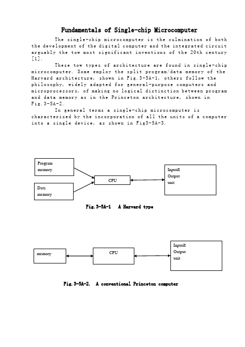
Fundamentals of Single-chip MicrocomputerTh e si ng le-ch i p mi cr oc om pu ter is t he c ul mi nat i on o f bo th t h e d ev el op me nt o f th e d ig it al com p ut er an d t he int e gr at ed ci rc ui ta r gu ab ly th e t ow m os t s i gn if ic ant i nv en ti on s o f t h e 20t h c en tury[1].Th es e to w typ e s of a rc hi te ctu r e ar e fo un d i n s in gl e-ch ip m i cr oc om pu te r. So m e em pl oy t he sp l it p ro gr am/d ata me mo ry o f th e H a rv ar d ar ch it ect u re, sh ow n in Fi g.3-5A-1, o th ers fo ll ow t hep h il os op hy, wi del y a da pt ed f or ge n er al-p ur po se co m pu te rs a ndm i cr op ro ce ss or s, of ma ki ng no lo gi c al di st in ct io n be tw ee n p ro gram a n d da ta m em or y a s i n th e Pr in cet o n ar ch it ec tu re,sh ow n inF i g.3-5A-2.In g en er al te r ms a s in gl e-chi p m ic ro co mp ut er i sc h ar ac te ri zed b y the i nc or po ra tio n of al l t he uni t s o f a co mp ut er i n to a s in gl e dev i ce, as s ho w n in Fi g3-5A-3.Fig.3-5A-1 A Harvard typeFig.3-5A-2. A conventional Princeton computerFig3-5A-3. Principal features of a microcomputerRead only memory (ROM).R OM i s u su al ly f or th e p er ma ne nt,n o n-vo la ti le s tor a ge o f an a pp lic a ti on s pr og ra m .M an ym i cr oc om pu te rs an d mi cr oc on tr ol le r s a re in t en de d fo r h ig h-v olume a p pl ic at io ns a nd h en ce t he e co nom i ca l ma nu fa ct ure of t he d ev ic es r e qu ir es t ha t the co nt en ts o f the pr og ra m me mo ry b e co mm it te dp e rm an en tl y d ur in g th e m an uf ac tu re o f c hi ps . Cl ear l y, th is im pl iesa ri g or ou s a pp roa c h t o R OM co de d e ve lo pm en t s in ce c ha ng es ca nnotb e m ad e af te r man u f a ct ur e .T hi s d e ve lo pm en t pr oce s s ma y in vo lv e e m ul at io n us in g a s op hi st ic at ed deve lo pm en t sy st em w i th a ha rd wa re e m ul at io n ca pa bil i ty a s we ll a s th e u se of po we rf ul so ft wa re t oo ls.So me m an uf act u re rs p ro vi de ad d it io na l RO M opt i on s byi n cl ud in g i n th ei r r a ng e de vi ce s wi th (or i nt en de d fo r us e with) u s er pr og ra mm ab le m em or y. Th e s im p le st of th es e i s us ua ll y d evice w h ic h ca n op er ate in a m ic ro pr oce s so r mo de b y usi n g so me o f th e i n pu t/ou tp ut li ne s as a n ad dr es s an d da ta b us f or acc e ss in g e xt er na l m e mo ry. T hi s t ype o f d ev ic e c an b e ha ve fu nc ti on al l y a s t he si ng le c h ip mi cr oc om pu te r fr om wh ic h i t i s de ri ve d a lb eit w it h r es tr ic ted I/O an d a mo di fie d e xt er na l ci rcu i t. T he u se o f t h es e RO Ml es sd e vi ce s is c om mo n e ve n in p ro du ct io n c ir cu it s wh er e t he v ol um e does n o t j u st if y th e d e ve lo pm en t co sts of c us to m on-ch i p RO M[2];t he re c a n st il l b e a si g ni fi ca nt s a vi ng in I/O a nd ot he r c hi ps co mp ared t o a c on ve nt io nal mi cr op ro ce ss or b as ed c ir cu it. M o re e xa ctr e pl ac em en t fo r RO M d ev ic es c an b e o bt ai ne d in t he f o rm o f va ri antsw i th 'pi gg y-ba ck'EP RO M(Er as ab le p ro gr am ma bl e ROM)s oc ke ts o rd e vi ce s w it h EP ROM i ns te ad o f R OM 。
- 1、下载文档前请自行甄别文档内容的完整性,平台不提供额外的编辑、内容补充、找答案等附加服务。
- 2、"仅部分预览"的文档,不可在线预览部分如存在完整性等问题,可反馈申请退款(可完整预览的文档不适用该条件!)。
- 3、如文档侵犯您的权益,请联系客服反馈,我们会尽快为您处理(人工客服工作时间:9:00-18:30)。
Clue of 1.1 introductionIn the current single chip has penetrated into every field of life, almost hard to find any area of single chip no footprints. Missile navigation device, the plane on various kinds of instrument control, computer network communication and data transmission, industrial automation process real-time control and data processing, the extensive use of all kinds of intelligent IC card, civilian luxury car security system, video, video camera, automatic washing machine control, and SPC toys, electronic pets, all of these cannot leave the microcontroller. Not to mention the automatic control system of intelligent instruments, robot, medical equipment. Therefore, the study of single chip, the development, and the application will create a number of computer application, and intelligent control of the engineers and scientists. The more advanced the science and technology, the intelligent the more things. Seems learning MCU is the inevitable result of social development needs.SCM namely single chip computer, also known as micro controller, its small size, the function is strong, good reliability and cheaper, become traditional industrial technology innovation and new products renewal ideal varieties, has broad prospects for development, one of the most representative is the 8051 series single chip Intel company.In this paper based on the study of the single chip microcomputer to AT89C51 as the core control chip, to digital electric clock for the design and application of its theory through thorough analysis and study the AT89C51 single-chip microcomputer constitutes the realization method of digital electric clock and introduced the design principle and method, give a digital clock software design. Considering the disturbance to the existence of the influence of the system, the software and hardware design from two aspects are analyzed, and the corresponding measures to improve the anti-interference ability of the system.1.2 to choose a backgroundNow on the market sell digital electric clock and its main function is dependent on digital circuit the function module combination to fulfill. These digital clock chip combination and connections can be difficult, and welding process is more complex, relative cost is higher, in order to overcome these shortcomings, and can fit a variety of situations, so the graduation design chose to use on the single chip computer programming based digital electric clock to meet the needs of more people. This is mainly through software programming to complete, so you reduce the complexity of the hardware circuit, and the cost is reduced, get rid of the digital circuit design of complex bring circuit, the welding process is complicated, the higher cost disadvantage. To design digital electric clock fully mining of the single chip computer resources and operation control ability. Has the function is much, show the advantages.. 2 single chip structureThe single chip microcomputer 8051 include the central processor, program memory (ROM), data memory (RAM), time/counter, parallel interface, serial interface and interrupt system and so on several big unit and the data bus, the address bus and control bus, the three big bus, now respectively to illustrate:The central processor: the central processing unit (CPU) is the core component of the single chip microcomputer, is 8 bits of data wide command and scheduling the whole unit degrees processor, can deal with eight binary data or code, the CPU is responsible for control, coordinate system work, complete the operation and control of input and output functions and other operational [2].Data memory (RAM) : 8051 internal has 128 eight user data storage unit and 128 special register units, which is unified addressing, special register can only be used to store data control instruction, users can only access, and cannot be used to store data, so customers can use RAM only 128, can deposit, speaking, reading and writing data, the middle of the operation result or user defined word list.Program memory (ROM) : 8051 4096 eight mask exposure ROM, used to store the user program, the raw data or form.Timing/counter ((ROM) : 8051 has two 16 bit programmable timing/counter, in order to achieve timing or count for control program to produce interrupt.Parallel input/output (I / 0) mouth: 8051 altogether 4 group eight I / 0 mouth (P0, P1, P2 and P3), used for external data transmission.Full-duplex serial mouth: 8051 built-in a full-duplex serial communication mouth, used to with other equipment serial data transfer between the, the serial port can be used for both the asynchronous communication transceiver, also can when synchronous shift implement use.Interrupt system: 8051 has the perfect interrupt function, two external interruption, two time interrupt, can meet different control requirements, and has a level 2 priority level of choice.The clock circuit: 8051 built-in highest frequency up to 12 MHz clock circuit, used to produce the whole SCM operation of the pulse timing, but 8051 single chip microcomputer to external oscillation capacitance.The structure of the single chip microcomputer there are two kinds, one kind is program memory and data storage separate form, namely Harvard ((Harvard) structure of the 8051 series microcontroller. INTEL by the Harvard of the form, the structure of the subsequent product 16 8096 series single chip used the Princeton structure.MCU is A kind of integrated circuit chip, using the technology with large scale data processing ability (such as arithmetic operations, logic operations, data transfer, interrupt handling) of the microprocessor (CPU), random access data memory (RAM), read only memory (ROM) program, input/output circuit (I / 0 mouth), may also include timing counter, serial communication mouth (SCI), display driver circuit (LCD or LED drive circuit), pulse width modulation (PWM), circuit (simulated roadconverter and more than A/D converter circuit such as integrated into A single chip, constitute A minimum however perfect computer system. These circuit in software can under the control of the accurate, rapid and efficient program designers set to complete the task of this view, SCM. A microprocessor doesn't have function, it can complete modern industrial control alone for the intelligent control function, this is the biggest single chip features. However microcontroller is different from single trigger, chip in no development, it just before the strong function have very large scale integrated circuit, if give it specific procedures, it is one of the smallest, complete micro computer control system, its single trigger or personal computer (PC) the distinction that having essence, the application of the single chip microcomputer chip level application, need to belong to the structure of the single chip microcomputer chip users understand the instructions and system, and other applications of integrated circuits technology and system the needs of design theory and the technology, with such specific chip design application, so that the chip has A specific function [3]. Different SCM has different hardware features and software features, which is that they are not the same technical characteristics, hardware features depends on the single chip microcomputer chip, the internal structure of the user to use a single chip microcomputer, must know this type of product meets the need of the function and application system requirements of the characteristic parameters. Here's a technical features include the functional characteristics, control characteristic and electrical characteristics and so on, these information from manufacturers need to get the technical manuals. Software features is refers to the instruction system characteristics and development support environment, instructions that we are familiar withsingle-chip characteristics of addressing mode, data processing and logical process method, input/output characteristics and the requirements, etc. Development support environment including instruction of compatible and portability, support the software (including can support the development of the application software resources) and hardware resources. To use a certain type of single chip microcomputer develop theirown application system, to master its structure characteristics and technical features is a must.Single-chip microcomputer control system can be replaced by complex electronic circuit or before digital circuit consists of the control system, the software control can to achieve, and to realize intelligent, now single-chip microcomputer control category is everywhere, such as communication products, household appliances, intelligent instruments, process control and special control device and so on, the application field of single chip microcomputer more and more widely.Admittedly, the single chip microcomputer application meaning far not limited to its application category or with the economic benefit from this, more important is it has fundamentally changed the traditional control method and design thought. Control technology is a revolution, is an important milestone.2.2.1 program memory8051 has 64 kB program storage addressing space, it used to store the user program, data and form and other information. For without the ROM 8031 single chip inside, it must be external program memory address space for 64 kB, at this time of the single chip microcomputer EA must be grounded and forced from outside the CPU program memory read program. For the ROM 8051 single chip microcomputer and normal operation will need to meet high level, make the CPU first from the interior of program storage read the program, when the PC value more than internal ROM capacity, they will turn to external program memory read program.There were 8051 pieces of the storage unit 4 kB program, its address forOOOOH-OFFFH, microcontroller start reduction, the content of the program counter for OOOOH, so the system will begin to carry out the program from OOOOH unit [4]. But in some of the special program storage unit, this in use should take note: one group of special unit is OOOOH-0002 H unit, the system restoration, PC for OOOOH, microcontroller OOOOH unit from begin to carry out the program, if the program is not from OOOOH unit started, should be in the three units for a unconditional jumpinstruction, let the CPU go directly to execute user specified programs. Another group of special unit is 0003 H-002 AH, this 40 units each have use, they are evenly divided into five sections, they are defined as follows:0003 H-000 AH external interruption 0 break address area OOOBH-0012 Htime/counter 0 interrupt site area.0013 H-001 AH external interruption 1 break address area 001 BH-0022 Htime/counter 1 interrupt site area.0023 H-002 AH serial break address area more than 40 unit of visible is used exclusively for the interrupt handlers address unit, the interrupt response, according to interrupt type automatic transfer to their interrupt area to the execution procedures. Therefore the above address unit cannot be used to store the other program content, only for the interrupt service routine. Generally, each segment of only eight address unit is can't save complete the interrupt service routine, and thus the general also in response to address area was interrupted a unconditional jump instruction, pointing to the other real program memory store the interrupt service routine space to perform, such interruption after response, the CPU read this transfer instructions article, turned to other place to continue the interrupt service routine.2.2.2 data storageData storage is also known as random access memory data [2]. Of 8051 single chip computer data storage in physics are points and logic for two address space, a is the internal data storage area and an external data storage area. 8051 128 256 or internal RAM byte of user data storage, they are used to store the execution of the intermediate results and process data. 8051 data storage are both, part of the unit can be a addressing.8051 internal RAM there are 256 units, the 256 units is divided into two parts. One is from OOH-7 FH address unit (a total of 128 bytes) for user data RAM. From the 80 H-FFH address unit (and 128 bytes) for special register (SFR) units. In OOH-1 FH of32 elements of is evenly divided into four pieces, each containing eight eight registers, all with RO-R7 to name, often say these registers for general-purpose registers. Internal RAM 20 H-2 FH unit for a addressing area, either as general unit with byte addressing, may also to their bit addressing. A addressing area there are 16 bytes, 128 bits, a address OOH-7 FH.2.2.3 special function registersSpecial function registers (SFR), also known as special register, special function registers reflect the single chip microcomputer 8051 operation. Many functions also through the special function registers to define and control [7] [8].8051 there are 20 special function registers, they are discrete distribution within the RAM in 80 H-FFH address, the hosting of function has made the special stipulation, the user can't modify the structure. The program Counter PC (program Counter) : it does not belong to the special internal data memory piece of PC is a 16 bit Counter, used to store a command to run address, addressing scope for 64 kB PC has to be automatic add 1 function, which finished the execution of an instruction, its content to be automatic plus one. PC itself and no address, and therefore not addressing, users can, speaking, reading and writing, but can be by transfer, calls, return to change its content and instructions, to control procedures according to the requirement to carry out.Accumulators ACC (Accumulator) : is a the most commonly used special register, most of the single operation instruction of a number of operation from accumulators, a lot of operation instruction of a number of operating number also taken from accumulators. Add, subtract, multiply and divide operation instruction, operation results are stored in an accumulator A or AB accumulators to. Most of the data operation will be through A accumulators8051 single chip microcomputer instruction 2.2.4 timingTiming is use to describe the timing of the unit, the unit of the succession of the 8051 there are four, they were beats, and state, machine cycle and the instruction cycle, the next explained respectively.The beat and state: the oscillation pulse cycle is defined as the beat (for the convenience of description, with P says), oscillation frequency pulse after dichotomy is then get the whole SCM systems of work the clock signal, put the clock signal cycle defined as state (in S said), such a state have two beat, the first half of the cycle of the corresponding beat defined as 1 (P), half a cycle after the corresponding beat defined as 2 (P). Machine cycle:8051 have fixed machine cycle, regulations, a machine cycle has six state, respectively, said S1-' S6 '.And a state contains two beat, so a machine cycle will have 12 beat, can remember SIP2, SIP2...... S6P1, S6P2, a machine cycle of these 12 oscillation pulse, namely machine cycle is oscillation pulse frequency 12 points, obviously, if use 6 MHZ clock frequency, a machine cycle that is 2 us, and such as the use of 12 MHZ clock frequency, a machine cycle is lus.The instruction cycle: to execute a directive need time is called an instruction cycle, 8051 instructions single-byte, double byte and three bytes of, so their instruction cycle is not the same, that they are the machine cycle is not same, may include one to four vary machine cycle.8051 the instructions of the timing: 8051 command system, according to their length can be divided into single-byte instructions, double byte instructions and three bytes instructions. The time needed to carry out these instructions is different, also is the machine cycle for them is different, have the following form: single-byte order machine cycle; Single-byte command double machine cycle; Double byte order machine cycle; Double byte command double machine cycle; Three bytes command double machine cycle; Single-byte instructions four machine cycle (such assingle-byte mentalistic method instruction).Single-byte single cycle instructions: single-byte single cycle instructions just once read operation instructions, when the second ALE signal effectively, the PC is not add 1, read or the original instructions, belong to an invalid read operation.Double byte single cycle instructions: these instructions two ALE signal are effective, just the first ALE is effective signal read operation codes, the second ALE signal when the operation is effective read several.Single-byte double cycle instructions: two machine cycle to read operation instructions four times, but only once read operation is effective, the last three of read operation are invalid operation.Single-byte double cycle instructions have a special kind of situation, like MOVX these instructions, perform these instructions, first read the instructions in ROM, then external data memory read or write operation, head of a machine cycle first read the instructions for the effective operation codes, and the second reading instruction is invalid operation. In the second the instruction cycle, the external data memory access, at this moment, ALE its operations without signal effects, which won't have read instructions operation action.External program memory (ROM) read timing: 8051 external program memory read sequence chart PO mouth when provide low eight address, P2 mouth provide high eight address, S2 before the end of the mouth of the PO low eight address is effective, appears later in the mouth of the PO it is no longer is the low eight address signals, but command data signals. Of course address signals and instructions data signals have a buffer between the excessive time, it is required in the low during the S2 must be eight address signals lock to save up, and then choose the pulse with ALE is to control the latches low eight address to latch, P2 mouth only output address signal, but no instruction data signals. The whole machine cycle address signals are effective, there is no need latch address signals.From external program memory read instructions, must have two signal control, in addition to the ALE signal, and a PSEN (external ROM read choose the pulse). PSENbegan to effective until will address signals sent out and external program memory storage data read only the CPU failure, then started the second S4P2 from reading instruction operation.External data memory (RAM) read timing: in the ROM to read from the execution of an instruction and CPU data storage visit is external to RAM data read or write operation, belong to the instruction of the execution cycles, read or write are two different machine cycle, but their timing is similar, only the timing of RAM read for analysis.On a machine cycle is take refers to the stage, read the instructions from ROM data, then the next cycle began to read the external data memory the contents of the RAM. In after the S4, first the need to read the address on the bus RAM, including PO mouth low eight address AO-A7 and P2 mouth of high eight address the A8-A15. When the pulse effective choose RD, will the data through the PO RAM the data bus read into the CPU. The second machine cycle of ALE signal still remains, a external ROM of read operation, but this time of read operation belong to the invalid operation.On the outside RAM write operation, the CPU output is WR (write choose communication number), data through the P0 data bus written in the external storage.2.2.5 8051 single chip microcomputer input output8051 have four groups eight 1/0 mouth: P0, P1, P2 and P3 mouth, P1, P2 and P3 shall prevail two-way mouth, PO mouth is two-way three states input output, this paper introduces some respectively the mouth line:PO mouth and P2 mouth: PO mouth and P2 mouth circuits contain a data output latches and two three states data input buffer, in addition to a data output drive and control circuit. The two groups as CPU and mouth line to external data storage, external program memory and I / 0 expand mouth, not like Pl, P3 directly used for export to lose. Together they can as an external the address bus, PO mouth wearing two hats, either as the address bus, but also as a data bus [5] [7].P2 mouth as an external data storage or program memory address bus high eight outlets AB8-AB15. PO by ALE choose the mouth as the address bus low eight output ABO-AB7. External program memory PSEA signal by choose the, the data storage by the WR and choose the reading and writing signal RD, 8051 the maximum external64 kB of memory and program data storage.P1 mouth: P1 mouth for eight must two-way mouth, each all can separate defined as input or lost export, when as input port, one writes latches, Q (not) = 0, the resistance will pull in potential pull to "1", while the mouth output is 1, when 0 written to the latches, Q (not) = 1, the output is 0.As input port, latches buy l, Q (not) = 0, at this time, this bit can put an external circuit drawn into a low level, can also be made by internal resistance and pulling into the high level, and because of this reason, P1 mouth often called must two-way mouth. Need to explain, as input mouth when using, have two kinds of cases, one is: the first is to read the content of the latches, deal with again after wrote latches, this kind of operation that is reading a modified a write operation, like JBC (logical judgment), CPL (to take the), INC (increase), DEC (decreasing), ANL (and logic) and ORL (logic or) command all belong to this kind of operation. The second is: read P1 mouth line condition, open three states door G2, external state will read the CPU.P3 mouth: P3 mouth shall prevail two-way mouth, to adapt to the second function of pin the need, increase the second function control logic, in a real application circuit, the second function is more important. Because the second function input and output signal has two kinds of circumstances, explained respectively. P3 input/output and mouth to mouth latches, interruption, time/counter, a serial port and special function on the register, the first function and mouth to mouth the same as input to the P1 output port, also have a byte operation and a operation two ways and operation mode in the next, each all can be defined as the input or output. Focuses on the discussion of the function of the second P3 mouth to mouth the second function of each tube feet are defined as follows:P3.0 serial input port (RXD)P3.1 serial outlets ((TXD)P3.2 external interruption 0 (INTO)P3.3 external interruption 1 (INT1)P3.4 timing/counter 0 of the external input mouth (TO)P3.5 timing/counter 1 external input mouth (T1)P3.6 external data memory write choose the (WR)P3.7 external data memory read choose the (RD)The second function as output pin, as I / 0 mouth use, a second function signal lines should keep high level and sr opening, in order to maintain from latches to output data output pathways clear. As a second function mouth line breaking, this bit of latches buy high level, and on the second function of sr signal output is clear, so as to realize the function of the second signal output. For the second function for input signal pin, in the mouth of the online access input opening a buffer, input signal is the second function of the output from the buffer to obtain. And as I / 0 mouth line input when taken from three states of the output buffer. So, whether it is as the input port use or the second function signal input, output circuit of the latches output and the second function signal output shall buy "1".2.2.6 8051 timing/counterThere are two of the 8051 single chip microcomputer 16 programmabletiming/counter [3], they have four work methods and its control word and state are in the corresponding word special function registers, the control register programming can choose the proper way of working.8051 single chip microcomputer timer of internal TO register special function by TLO (low eight) and THO (high eight) constitute, timer by special function by T1 registers TLl (low eight) and TH1 (high eight) constitutes.Special function TMOD registers control timed registers way of working and TCON is used TO control the timer and T1 TO the start and stop counting, and at the same time management timer and T1 spillover TO mark etc. TO begin the process need TO TL0, THO, TL1 and TH1 initialization TO programming, defining their way of working and control and the count TO T. Timing/counter way to control word TMOD, byte address for 89 H, the format such as table 2.5:Table 2.5 TMOD registers structureD7 D5 D6 D4 D3 D2 D1 D0GATA C/T M1 M0 GATA C/T M1 M0T1 way prearcing field way fieldTable 2.6 TCON structureD7 D5 D6 D4 D3 D2 D1 D0TF0 TR0 TR1 TF1 has been presented IE1 IT1 IE0 IT0Note that the TCON DO-D3 a and interrupt relevant, in interrupt the content of will to illustrate, 8051 of the timing/counter there are four work way, carry on the discussion. Work way 0Timing/counter 0 way of working 0 is the 13 patients count work style of the structure, the counter all by TH eight and low five constitute the TL, TL high three no use. When C/T = 0, multi-channel switch oscillation frequency output pulse 12 points, and a counter to count in turn, this is timing way to work. When C/T = 1, multi-channel switch count pin (To), external count by pin pulse To input. When the count pulse generating negative jump to change, counter add 1, this is count way to work. No matter what kind of work way, when the low five TL overflow, will be to TH carry, and all 13 a counter overflow, the spill to counter sign a TFO respectively.A state of GATA decision timer operation control depends on a condition or TRO TRO and pins INTO these two conditions. When GATA = O, and the output of thedoor is driven by TRO and INTO the state level to determine, if this time TRO = 1, INTO = 1 and door for 1 output, allow time/counter count, in this case, the operation control and work by TRO NTO two conditions common control, TRO is suretiming/counter operating control a, by the software for a or clear "0". As mentioned above, the counter is regular/TFO overflow condition sign, overflow by the hardware for a, TFO overflow interrupts are responding to a CPU, turn to the disruptions hardware qing "0", TFO can also be made by program inquires "0" and clear.In the way under the 0, counter plan of numerical limits is 1-8192 (). For regular work way, the timing of the time formulas for the: (a) X initial count crystals cycle X12 or (a count initial value) X machine cycle, unit of time and crystals cycle or machine to the same cycle.Work way 1When M1M0 = 01, timing/counter at work mode 1. Way the difference between 0 and 1 only way is to counter the number is different, the way a 0 for 13, and 1 is way 16, THO as high by eight, TLO for low 8 bits, the relevant control state words and the same way 0.In the way of working under 1, counter plan of numerical limits is 1-65536 (), when the timing for work in the way one, the timing of the time formulas for the: (a) X initial count crystals cycle X12 or (a count initial value) X machine cycle, the unit of time and crystals cycle or machine to the same cycle.Work mode 2M1M0 = 10, timing/counter in mode 2 work. Way to work and work methods 1 0 that the biggest characteristic of count after the spill, the counter to all the 0, thus cycle time or cycle count application there is a repeated initial value problems of set, this to the program designed to bring a lot of inconvenience, also affect timing precision. Work on this question 2 way and Settings, it has to be automatic heavy load function, namely, to be automatic loading count initial value, so also known as automatic heavy loading way to work. In this way of working, 16 counter was divided into two parts,。