skiip模块说明
SKIIP12NAB126V1中文资料
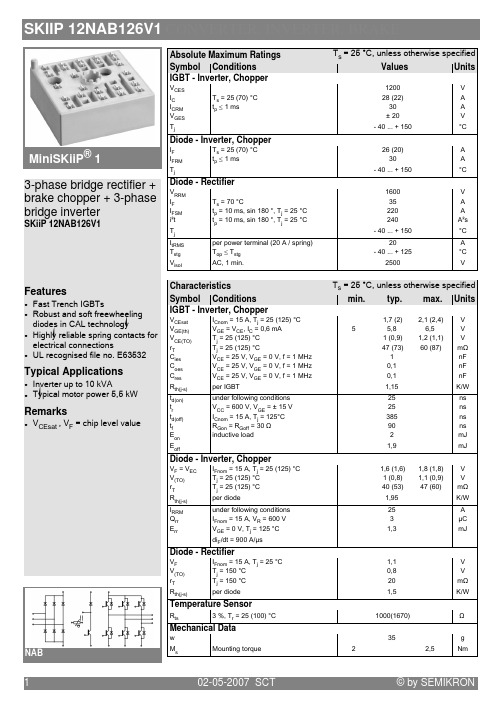
Features
!
"
# $%&'&( Typical Applications )
! *+ ,- ! .
!
'/' ,0 Remarks -$ / - 1 ! ) )
NAB
Characteristics
Symbol Conditions IGBT - Inverter, Chopper
-$ -$57 -$5 B7
02-05-2007 SCT
© by SEMIKRON
元器件交易网
SKIIP 12NAB126V1 CONVERTER, INVERTER, BRAKE
Fig. 7 Typ. gate charge characteristic
Fig. 8 Typ. thermal impedance
A 1 C++ AI
Diode - Rectifier
- -5 B7
. 1 *' / < 1 (' 2 < 1 *'+ 2 < 1 *'+ 2
5<=7
!
Temperature Sensor
& J/
1 (' 5*++7 2
Mechanical Data
Absolute Maximum Ratings Symbol Conditions IGBT - Inverter, Chopper
SKIIP32NAB12T1中文资料

& &
$& PLQ
9DOXHV
± ±
8QLWV
9 9 $ $ $ $
9 $ $ $V & & 9
&KDUD.WHULVWL.V
(RQ (RII
&LHV
9&( 9 9*( 9 0+]
5WKMK
SHU ,*%7
,*%7 &KRSSHU
±
±
±
±
±
±
±
±
±
±
±
9&(VDW ,& $ 7M &
WG RQ
9&& 9 9*( 9
Eoff
180 Ω
20 V
15
10
600V
, ms31nab12t11.xls - 5
&SXOV
$
10 nF
1 800V
ms31nab12t11.xls - 6
Ciss
9*( 9 I 0+]
Coss
5
VGE
0
0
40
QGate
80
120
160
200
nC
)LJ 7\S JDWH .KDUJH .KDUD.WHULVWL.
Comchar1200V.xls-12
max.
Tvj=125°C
50 IFop / IF
Tvj=25°C
0
SKIIP13NAB065V1中文资料

SKiiP 13NAB065V1 CONVERTER, INVERTER, BRAKE
MiniSKiiP® 1
3-phase bridge rectifier + brake chopper + 3-phase bridge inverter
SKiiP 13NAB065V1
4
02-05-2007 SCT
© by SEMIKRON
typ.
max. Units
) 6)+)8 )+( 6)+78 -
'
9
(
-
:+) 6:+:8 :+' 6:+)8 -
(' 67'8 ;/ 6://8 .F
/+77
1
/+:)
1
/+/&
1
:+9
HD0
)/
'/
:B(
:/
/+&
.I
/+'
.I
:+9 6:+98 :+7 6:+78 -
: 6/+B8 :+: 6:8
'/
> )/
-
@ 9/ $$$ A :(/
3
)& 6:B8
'/
@ 9/ $$$ A :(/
3
;//
-
'
C
@ 9/ $$$ A :(/
3
)/
@ 9/ $$$ A :)(
SKIIP32NAB12中文资料
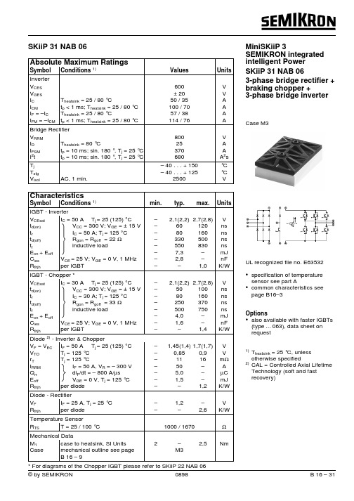
© by SEMIKRON 0898B 16 – 31Absolute Maximum RatingsSymbol Conditions 1)Values Units Inverter V CES V GES I C I CMI F = –I C I FM = –I CMT heatsink = 25 / 80 °Ct p < 1 ms; T heatsink = 25 / 80 °C T heatsink = 25 / 80 °Ct p < 1 ms; T heatsink = 25 / 80 °C600± 2050 / 35100 / 7057 / 38114 / 76V V A A A A Bridge Rectifier V RRM I D I FSMI 2t T heatsink = 80 °Ct p = 10 ms; sin. 180 °, T j = 25 °C t p = 10 ms; sin. 180 °, T j = 25 °C 80025370680V A A A 2s T j T stg V isol AC, 1 min.– 40 . . . + 150– 40 . . . + 1252500°C °C VSKiiP 31 NAB 06MiniSKiiP 3SEMIKRON integrated intelligent Power SKiiP 31 NAB 063-phase bridge rectifier +braking chopper +3-phase bridge inverterCase M3UL recognized file no. E63532•specification of temperature sensor see part A•common characteristics see page B16–3Options•also available with faster IGBTs (type ... 063), data sheet on request1)T heatsink = 25 °C, unless otherwise specified2)CAL = Controlled Axial Lifetime Technology (soft and fast recovery)* For diagrams of the Chopper IGBT please refer to SKiiP 22 NAB 06B 16 – 320698© by SEMIKRONFig. 3Turn-on /-off energy = f (I C )Fig. 4Turn-on /-off energy = f (R G )T j = 125 °C V CE = 300 V V GE = ± 15 V I C = 50 AT j = 125 °C V CE = 300 V V GE = ± 15 V R G = 22 ΩI Cpuls = 50 AV GE = 0 V f = 1 MHzFig. 1Typ. output characteristic, t p = 80 µs; 25 °CFig. 2Typ. output characteristic, t p = 80 µs; 125 °CFig. 5Typ. gate charge characteristic Fig. 6Typ. capacitances vs. V CE© by SEMIKRON0698B 16 – 3Fig. 9Turn-off safe operating area (RBSOA) of the IGBT Fig. 10Safe operating area at short circuit of the IGBTT j= ≤ 150 °C V GE = ± 15 V t sc = ≤ 10 µs L ext < 25 nHT j = ≤ 150 °C V GE = ± 15 VFig. 7Rated current of the IGBT I Cop / I C = f (T h )T j = 150 °C V GE = ≥ 15 V00.20.40.60.81.01.2255075100125150I Cop /I C Mini0607T h [°C]Fig. 11Typ. freewheeling diode forward characteristic Fig. 12Forward characteristic of the input bridge diode mon characteristics of MiniSKiiPMiniSKiiP 600 VMiniSKiiP 3SKiiP 30 NAB 06 SKiiP 31 NAB 06 SKiiP 32 NAB 06 SKiiP 30 NAB 12 SKiiP 31 NAB 12 SKiiP 32 NAB 12CircuitCase M3Layout and connections for thecustomer’s printed circuit board。
SEMIKRON SKiip 智能功率模块 说明书

S E M i N E W S賽米控專刊赛米控中国於2009年下半年的活动概览:7月9日赛米控风力发电技术研讨会 (北京)9月11日第三届电力电子创新技术及解决方案研讨会(太陽能光伏發電) (常州)10月21-23日北京国际风能大会暨展览会 (北京)(展台號1B09)11月6-8日第十五届中國電動車輛學術年會 (上海)第四期 Issue 4 (2009年8月)sKiiP ® 4 — 市场上輸出電流最大的智能功率模塊sKiiP ® 4,新一代智能功率模块(IPM),相比采用焊接工艺的模块,其使用寿命更长,工作温度更高。
sKiiP ® 4是目前市场上輸出電流最大的智能功率模块,比之前的sKiiP ® 3 , 其輸出功率提高了33% 。
sKiiP ® 4 IPM 主要用于风能和太阳能应用、電力牵引、电梯系统以及大功率的工業驅動。
赛米控技术研讨会在中国三地圆满结束第四期 (2009年8月) P2借助 SKiiP® 4 开发更强大、结构更紧凑的变频器,从而降低成本。
功率的增加依赖于使用了创新压接系统、改进的散热器以及IGBT4 、CAL4芯片技术。
此外, 該模塊首次使用6个并联的半桥,而非目前所普遍采用的4个半桥。
SKiiP® 4模块中,半导体芯片不是焊接到陶瓷基板上,而是采用烧结技术连接,这意味些实验,可以识别早期产生的硅失效并将有缺陷的芯片清除。
实验中,模块是被暴露在最大可能结温下。
无焊接压接系统和集成的叠层母線确保均匀的电流分布。
每个IGBT和二极管芯片单独连接到主端子上,使模块內阻抗很低。
这些芯片不是焊接到陶瓷基板上,而是通过烧结过程连接。
由于这些模块没有底板,DCB和离,这意味着用户无需提供额外的隔离。
为了更加完美,新 SKiiP® 4 IPM还有一个多级输出级,以减少过电压,输出级中还包括其他各种保护功能。
最后,在用户侧还提供优化评估的诊断通道。
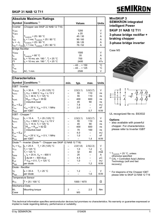
SKIIP31NAB12T11中文资料
µV & 7M & 9&( 9 9*( 9 ,& $
ms31nab12t11.xls - 3
ms31nab12t11.xls - 4
Eon
15
Eon
10 Eoff 5 E 0 0 IC 20 40 60 A 80 E
10
5
Eoff
0LQL6.LL3
6.LL3 1$% 7 6.LL3 1$% 7 6.LL3 1$% 7
E\ 6(0,.521
7ROHUDQ.H ,62 I
E\ 6(0,.521
元器件交易网
6.LL3 1$% 7
70 A 60 50 40 30 20 10 IC 0 0 VCE 1 2 3 17V 15V 13V 11V 9V 7V
ms31nab12t11.xls - 1
70 A 60 50 40 30 20 10 IC 0 17V 15V 13V 11V 9V 7V
)LJ 7\S IUHHZKHHOLQJ GLRGH IRUZDUG .KDUD.WHULVWL.
E\ 6(0,.521
)LJ )RUZDUG .KDUD.WHULVWL. RI WKH LQSXW EULGJH GLRGH
元器件交易网
&DVH 0
%ULGJH 5H.WLILHU 7KHDWVLQN & WS PV VLQ 7M WS PV VLQ 7M
& &
$& PLQ
&KDUD.WHULVWL.V
6\PERO &RQGLWLRQV
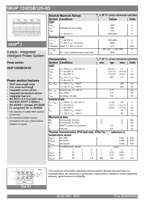
SKIIP1242GB120-4D中文资料
This technical information specifies semiconductor devices but promises no characteristics. No warranty or guarantee, expressed or implied is made regarding delivery, performance or suitability.
1
/
min. typ. max. Units
: :<
8 # C 7B 8 ", &#",' 9 7B 8 ", &#",' 9 7B 8 ", &#",' 9
:? 8 :C : 8 :C
7B 8 ", &#",' 9
28-02-2007 HER
© by SEMIKRON
元器件交易网
SKiiP 1242GB120-4D INTEGRATED DRIVER, SENSORS
SKiiP® 2
Absolute Maximum Ratings Symbol Conditions
:# :" :J
C
=$2 5
& '
<5
<5
5
5( :< :#" /1 / 7 &7 '
2.
#, : 1
赛米控丹佛斯 MiniSKiiP IGBT模块 SKiiP 26GB12F4V1 数据表

© by SEMIKRONRev. 3.0–24.09.20211MiniSKiiP ®2 DualHalf-BridgeSKiiP 26GB12F4V1Features*•Fast Trench 4 IGBTs•Robust and soft freewheeling diodes in CAL technology•Highly reliable spring contacts for electrical connections•UL recognised: File no. E63532•NTC T-SensorRemarks•Max. case temperature limited to T C =125°C•Product reliability results valid for T j ≤150°C (recommended T j,op =-40...+150°C)Absolute Maximum Ratings SymbolConditionsValuesUnitInverter - IGBTV CES T j =25°C1200V I C λpaste =0.8 W/(mK)T j =175°C T s =25°C 197A T s =70°C 158A I Cλpaste =2.5 W/(mK)T j =175°C T s =25°C 257A T s =70°C208A I Cnom 200A I CRM 400A V GES -20 (20)V t psc V CC =800V V GE ≤ 15V V CES ≤ 1200VT j =150°C10µs T j -40...175°C Inverse - DiodeI F λpaste =0.8 W/(mK)T j =175°C T s =25°C 194A T s =70°C 154A I F λpaste =2.5 W/(mK)T j =175°C T s =25°C 219A T s =70°C174A I FRM 400A I FSM 10ms, sin 180°, T j =150°C 990A T j -40 (175)°C Module I t(RMS)T terminal =80°C, 20 A per spring 200A T stg module without TIM -40...125°C V isolAC sinus 50 Hz, t =1min 2500VCharacteristics SymbolConditionsmin.typ.max.UnitInverter - IGBTV CE(sat)I C =200A V GE =15V chiplevelT j =25°C 2.05 2.42V T j =150°C 2.59 2.96V V CE0chiplevel T j =25°C 1.10 1.28V T j =150°C 0.95 1.13V r CE V GE =15V chiplevelT j =25°C 4.8 5.7m ΩT j =150°C8.29.2m ΩV GE(th)V GE = V CE , I C =7.6mA5.25.86.4V I CES V GE =0V,V CE =1200V, T j =25°C 2.0mA C ies V CE =25V V GE =0Vf =1MHz 12.30nF C oes f =1MHz 0.81nF C res f =1MHz0.69nF Q G V GE =- 8 V...+ 15 V 1134nC R Gint T j =25°C 3.8Ωt d(on)V CC =600V I C =200A R G on =2ΩR G off =2Ωdi/dt on =4100A/µs di/dt off =2500A/µs V GE =+15/-15VT j =150°C 167ns t r T j =150°C 52ns E on T j =150°C 16.8mJ t d(off)T j =150°C 414ns t f T j =150°C 52ns E off T j =150°C 16.3mJ R th(j-s)per IGBT, λpaste =0.8 W/(mK)0.25K/W R th(j-s)per IGBT, λpaste =2.5 W/(mK)0.16K/W2Rev. 3.0–24.09.2021© by SEMIKRONMiniSKiiP ®2 DualHalf-BridgeSKiiP 26GB12F4V1Features*•Fast Trench 4 IGBTs•Robust and soft freewheeling diodes in CAL technology•Highly reliable spring contacts for electrical connections•UL recognised: File no. E63532•NTC T-SensorRemarks•Max. case temperature limited to T C = 125°C•Product reliability results valid for T j ≤150°C (recommended T j,op =-40...+150°C)Characteristics SymbolConditionsmin.typ.max.UnitInverse - DiodeV F = V EC I F =200AV GE =0V chiplevelT j =25°C 2.20 2.52V T j =150°C 2.15 2.47V V F0chiplevel T j =25°C 1.30 1.50V T j =150°C 0.90 1.10V r FchiplevelT j =25°C 4.5 5.1m ΩT j =150°C6.3 6.9m ΩI RRM I F =200A di/dt off =3840A/µs V GE =-15VV CC =600VT j =150°C 189A Q rr T j=150°C28.7µC E rr T j =150°C 11.7mJ R th(j-s)per Diode, λpaste =0.8 W/(mK)0.34K/W R th(j-s)per Diode, λpaste =2.5 W/(mK)0.28K/W Module L CE 20nHM s to heat sink 22.5Nm w50g Temperature Sensor R 100T c =100°C (R 25=5 k Ω)493 ± 5%ΩB 25/85R (T)=R 25*exp[B 25/85*(1/T-1/298)], T[K]3420K© by SEMIKRON Rev. 3.0–24.09.202134Rev. 3.0–24.09.2021© by SEMIKRON© by SEMIKRON Rev. 3.0–24.09.20215This is an electrostatic discharge sensitive device (ESDS) due to international standard IEC 61340.*IMPORTANT INFORMATION AND WARNINGSThe specifications of SEMIKRON products may not be considered as guarantee or assurance of product characteristics ("Beschaffenheitsgarantie"). The specifications of SEMIKRON products describe only the usual characteristics of products to be expected in typical applications, which may still vary depending on the specific application. Therefore, products must be tested for the respective application in advance. Application adjustments may be necessary. The user of SEMIKRON products is responsible for the safety of their applications embedding SEMIKRON products and must take adequate safety measures to prevent the applications from causing a physical injury, fire or other problem if any of SEMIKRON products become faulty. The user is responsible to make sure that the application design is compliant with all applicable laws, regulations, norms and standards. Except as otherwise explicitly approved by SEMIKRON in a written document signed by authorized representatives of SEMIKRON, SEMIKRON products may not be used in any applications where a failure of the product or any consequences of the use thereof can reasonably be expected to result in personal injury. No representation or warranty is given and no liability is assumed with respect to the accuracy, completeness and/or use of any information herein, including without limitation, warranties of non-infringement of intellectual property rights of any third party. SEMIKRON does not assume any liability arising out of the applications or use of any product; neither does it convey any license under its patent rights, copyrights, trade secrets or other intellectual property rights, nor the rights of others. SEMIKRON makes no representation or warranty of non-infringement or alleged non-infringement of intellectual property rights of any third party which may arise from applications. Due to technical requirements our products may contain dangerous substances. For information on the types in question please contact the nearest SEMIKRON sales office. This document supersedes and replaces all information previously supplied and may be superseded by updates. SEMIKRON reserves the right to make changes.6。
赛米控丹佛斯SKiiPRACK功率组件SKS C 120 GDD 69 11-A3A WA B1B数

Absolute maximum ratings 1)Symbol ConditionsUnit I IN MAX Maximum permanent input current (4Q only)A RMS I OUT MAX Maximum permanent output current A RMS V IN MAX Maximum input voltage (4Q only)V AC V OUT MAX Maximum output voltage V AC V BUS MAX Maximum DC Bus voltageV DC F IN MAX Inverter input frequency (4Q only)Hz F OUT MAX Inverter output frequencyHz F SW MAXMaximum switching frequency kHzElectrical characteristics: application example T AMBIENT=40°C unless otherwise specifiedSymbolConditionsmintypmaxUnitAC phase Grid I OUT RATED Rated output current (4Q) 1 200A RMS I OUT RATED Rated output current (2Q) 2 400A RMS I OUT OVL Overload output current (4Q) 1 320A RMS I OUT OVL Overload output current (2Q) 2 640A RMS t OVL Overload duration 60s SKiiPRACK® - Type 3AT OVL Time between 2 overloads 10min 3-phase IGBT converterV OUT Output voltage 620690760V AC P OUT Rated output power (4Q)1 430kW This stack can be used as a 2Q 3-phase inverter or a P OUT Rated output power (2Q)2 870kW 4Q converter. All values are valid for 2Q and 4Q F SWInverter switching frequency 2kHz configurations unless otherwise specified.F OUTOutput frequency50Hz PF Power factor1-P LOSS INV 2)Losses at rated current 14 160W Ordering No.08769360η2)Efficiency at rated current 99%Description 4Q / SKS C 120 GDD 69/11 – A3A MA B1CAC phase Generator (4Q only)2Q / SKS C 240 GD 69/11 – A3A MA B1CI IN RATED Rated input current 1 200A RMS I IN OVL Overload input current 1 320A RMS Featurest OVL Overload duration60s Designed in regard to EN50178 recommendations T OVL Time between 2 overloads 10min Designed for a 600 x 600 x 2000 mm cabinet V OUT Output voltage620690760V AC Embedded SKiiP® Technology 3P OUT Rated output power1 430kW SKiiP 2403GB172-4DW, Trench 3 1700V IGBT, CAL3 diode F SW Inverter switching frequency 2kHz Integrated current and temperature sensors F OUT Output frequency 20100Hz Water coolingPF Power factor-1-P LOSS INV2)Losses at rated current 14 160W Typical Applicationsη2)Efficiency at rated current99%Wind generators (SG and DFIG) High power AC drives DC Bus V BUSRated DC voltage applied to the capacitor bank1 100V DC FootnotesV BUS MAX Max DC voltage applied to the caps bank (max 30% of LTE) 1 200V DC 1)Absolute maximum ratings are values not to be τd 5%Discharge time of the capacitors (V DC < 60 V)6min exceeded in any case and do not imply that the stack C DC Capacitor bank capacity14,0mF can operate in all these conditions taken togetherLTECalculated LTE of the capacitors with forced air cooling100kh2) fan consumption and losses in air includedStack Insulation REMARKSCrd Minimum creepage distance 8,7 mm Cld Minimum clearance distance7,1 mm Visol Chassis / Power stage AC/DC (insulation test voltage DC, 5 s)-4 2004 200V DC Visol12SKiiP driver only, output 1 / output 2 (AC, rms, 2 s) 1 500V dv/dtSKiiP driver only, secondary to primary side75kV/µsValues 1 20076010052 4001001 200760SKiiP stackV BUS = 1 100 V DC T INLET = 45°C, 50% glycol Flowrate = 12 L/min per cellT J < 125°C Air extraction according to thermal data page 2V BUS = 1 100 V DCT INLET = 45°C, 50% glycol Flowrate = 12 L/min per cell T J < 125°CAir extraction according to thermal data page 2This technical information specifies semiconductor devices but promises no characteristics. No warranty or guarantee,expressed or implied is made regarding delivery, performance or suitability.Before using the converter, please read carefully the SKiiPRACK® user manual.Environmental conditions T AMBIENT=40°C unless otherwise specified Characteristics Conditions min typ max UnitAmbient temperature 1)HumidityInstallation altitude without derating 1 000mMax. installation altitude with derating4 000mProtection degreeIEC 60529IP00-IEC 60721-3-2, Storage & transportation, 1 cell2M1-IEC 60721-3-3, in operation, 1 cell3M3-Pollution degree EN 501782-Cell80kgFull converter275kgThermaldataSKiiPRACK® - Type 3A Water flow per cell81224L/min 3-phase IGBT converter Water flow per converter243672L/minPressure drop per cell, 50% glycol, 12 L/min130mbar This stack can be used as a 2Q 3-phase inverter or a Pressure drop per converter, 50% glycol, 36 L/min130mbar 4Q converter. All values are valid for 2Q and 4Q Water pressure Maximum water pressure permissible per cell3bar configurations unless otherwise specified.Coolant type Recommended coolant50% Glycol / 50% water-T INLET Cooling water inlet temperature-204560°CRequired cooling airflow Snubbers, airflow direction bottom-top1ms-1 Ordering No.08769360V SUPPLY[fan]Capacitor DC fan operating voltage182428V DC Description4Q / SKS C 120 GDD 69/11 – A3A MA B1C P FAN per fan Fan power consumption at typical voltage supply3,6W 2Q / SKS C 240 GD 69/11 – A3A MA B1C LTE[fan]Capacitor DC fan life time expectancy (L10 method)65kh Features Gate Driver Characteristics T AMBIENT=25°C unless otherwise specified Designed in regard to EN50178 recommendations Symbol Conditions min typ max Unit Designed for a 600 x 600 x 2000 mm cabinet Gate Driver / controler dataEmbedded SKiiP® Technology 3V S2 supply voltage non stabilized 132430V DC SKiiP 2403GB172-4DW, Trench 3 1700V IGBT, CAL3 diode I S2 VS2 = 13V - 30 V , F SW in kHz, I AC in A330 + 55×F SW + 0.00035×I AC2mA Integrated current and temperature sensors ViT+input threshold voltage HIGH 12.3V DC Water cooling ViT-input threshold voltage LOW 4.6V DCR IN Input resistance10kΩTypical Applications C IN Input capacitance1nF Wind generators (SG and DFIG)Measurement & protectionHigh power AC drives HB_I Analogue current signal I analog OUT245250255 A.V-1I TRIPSC over current trip level(Ianalog OUT=10V) 2 450 2 500 2 550A PEAK Footnotes min17 + 10,3×CMN_TMP°C 1) the user shall ensure that the ambient air is sufficiently CMN_TMP Analogue temperature signal Th < 80°C typ19 + 10,5×CMN_TMP°C ventilated to avoid hot spots.max20 + 10,5×CMN_TMP°Cmin26 + 8,8×CMN_TMP°CCMN_TMP Analogue temperature signal Th > 80°C typ28 + 8,8×CMN_TMP°Cmax30 + 8,9×CMN_TMP°C REMARKS T trip Over temperature protection110115120°CClimaticMechanicalSKiiP stack6085%IEC 60721-3, class 1K2&2K2Storage & transportationIEC 60721-3-3, class 3K3 extendedIn operation-25IEC 60721-3-3, class 3K3no condensation no icing°CVibrations & Shocks-2055°CThis technical information specifies semiconductor devices butpromises no characteristics. No warranty or guarantee,expressed or implied is made regarding delivery, performanceor suitability.Before using the converter, please read carefully theSKiiPRACK® user manual.∆P WATER5Mass∆V/∆t WATER4QHE10-14 male connectorDC+DC-Phase driver connectorsDC BUS detailsDC BUS connectionV W L3L2L1 2Q V1W1W2V2U2PinDesignation1+24VDC 2+24VDC 3GND 4GNDDC FAN CONNECTION (6 times)This technical information specifies semiconductor devices but promises no characteristics. No warranty or guarantee RIGHT SIDE VIEW FRONT VIEW12 3 4LEFT SIDE VIEWREAR VIEWThis technical information specifies semiconductor devices but promises no characteristics. No warranty or guarantee6200400600800100012001400303540455055O u t p u t c u r r e n t (A R M S )Ambient air temperature (°C)Cooling liquid 45°CCooling liquid 60°CV BUS = 1100 V DCVac IN/OUT =690 V RMS F IN/OUT = 50 Hz f SW IN/OUT = 2 kHz cos ϕIN/OUT = 1Flowrate = 12 L/min per cell Glycol/water ratio = 50%Altitude <1000 m2004006008001000120014005001000150020002500300035004000O u t p u t c u r r e n t (A R M S )Altitude (m)Cooling liquid 45°C, ambient 40°C Cooling liquid 60°C, ambient 55°CV BUS = 1100 V DCFlowrate = 12 L/min per cell Vac IN/OUT =690 V RMS Glycol/water ratio = 50%F IN/OUT = 50 Hz Altitude <1000 mf SW IN/OUT = 2 kHz cos ϕIN/OUT = 10100200300400500600510152025P r e s s u r e d r o p p e r S K i i P R A C K c e l l (m b a r )Flowrate (L/min)Pressure drop with 50% glycol Pressure drop without glycol (mbar)50010001500200025003000303540455055O u t p u t c u r r e n t (A R M S )Ambient air temperature (°C)Cooling liquid 45°C Cooling liquid 60°CV BUS = 1100 V DC Vac =690 V RMS F OUT = 50 Hz f SW = 2 kHz cos ϕ= 1Flowrate = 12 L/min per cell Glycol/water ratio = 50%Altitude <1000 m500100015002000250030005001000150020002500300035004000O u t p u t c u r r e n t (A R M S )Altitude (m)Cooling liquid 45°C, ambient 40°CCooling liquid 60°C, ambient 55°CV BUS = 1100 V DC Vac =690 V RMS F OUT = 50 Hz f SW = 2 kHz cos ϕ= 1Flowrate = 12 L/min per cell Glycol/water ratio = 50%00,0020,0040,0060,0080,010,0120,0145101520253035R t h (°C /W )Flowrate per cell (L/min)Stack Rth 50% glycol (°C/W)Stack Rth 10% glycol (°C/W)720040060080010001200140051015O u t p u t C u r r e n t (A R M S )AC Fundamental Frequency (Hz)Vdc = 1100 V DCVac IN/OUT =690 V RMS f SW IN/OUT = 2 kHz cos ϕIN/OUT = 1Water temperature = 45°C Flowrate = 12 L/min per cell Glycol/water ratio = 50%Air temperature = 40°C T J = 125°C050010001500200025003000200400600800100012001400M a x c u r r e n t s w i t c h e d (A )DC bus voltage (V)500100015002000250051015O u t p u t C u r r e n t (A R M S )AC Fundamental Frequency (Hz)Vdc = 1100 V DC Vac =690 V RMS f SW = 2 kHz cos ϕ= 1Water temperature = 45°C Flowrate = 12 L/min per cell Glycol/water ratio = 50%Air temperature = 40°C T J = 125°C。
赛米控丹佛斯 SKiiP IPM SKiiP 613 GD123-3DUL V3 数据表
SKiiP ®3SKiiP 613 GD123-3DUL V3Features•SKiiP technology inside •Trench IGBTs •CAL HD diode technology •DC-Link voltage monitoring •Integrated current sensor•Integrated temperature sensor •Integrated heat sink•UL recognized File no. E63532Typical Applications*•Renewable energies •Traction •Elevators•Industrial drivesFootnotes1)With assembly of suitable MKP capacitor per terminalSymbolConditions Values UnitSystem V CC 1)Operating DC link voltage900V V isol DC, t =1s, main terminals to heat sink 4300V I t(RMS)per AC terminal, T terminal <115°C 400A I FSM T j =150°C, t p =10ms, sin 180°3500A I²t T j =150°C, t p =10ms, diode 61kA²s f out fundamental output frequency 1kHz T stg storage temperature-40 (85)°CIGBT V CES T j =25°C 1200V I CT j =150°CT s =25°C 577A T s =70°C444A I Cnom 600A T j 2)junction temperature -40...150°C Diode V RRM T j =25°C 1200V I F T j =150°CT s =25°C 466A T s =70°C353A I Fnom 470A T j junction temperature -40...150°C Driver V s power supply13 ... 30V V iH input signal voltage (high)15 + 0.3V V isolPD QPD <= 10pC, PRIM to POWER 1170V dv/dt secondary to primary side 75kV/µs f swswitching frequency15kHzCharacteristics T s = 25°C unless otherwise specified SymbolConditions min.typ.max.UnitIGBT V CE(sat)I C =300A at terminalT j =25°C 1.7 2.1V T j =125°C 1.9V V CE0T j =25°C 0.90 1.10V T j =125°C0.80 1.00V r CE at terminal T j =25°C 2.6 3.3m ΩT j =125°C 3.7 4.4m ΩE on + E off I C =300A T j =125°C V CC =600V 110mJ V CC =900V195mJ R th(j-s)per IGBT switch 0.059K/W R th(j-r)per IGBT switch0.054K/WSKiiP ®3SKiiP 613 GD123-3DUL V3Features•SKiiP technology inside •Trench IGBTs •CAL HD diode technology •DC-Link voltage monitoring •Integrated current sensor•Integrated temperature sensor •Integrated heat sink•UL recognized File no. E63532Typical Applications*•Renewable energies •Traction •Elevators•Industrial drivesFootnotes1)With assembly of suitable MKP capacitor per terminalSymbolConditions min.typ.max.UnitDiode V F = V EC I F =300A at terminalT j =25°C 1.50 1.80V T j =125°C 1.50V V F0T j =25°C 0.9 1.10V T j =125°C0.70.90V r Fat terminal T j =25°C 2 2.3m ΩT j =125°C 2.73m ΩE rr I F =300A T j =125°C V R =600V 21mJ V R =900V28mJ R th(j-s)per diode switch 0.115K/W R th(j-r)per diode switch0.174K/W DriverV s supply voltage non stabilized 132430V I S0bias current @V s =24V, f sw = 0, I AC = 0420mA I sk 1=42mA/kHz, k 2=0.00211mA/A 2= 420+ k 1* f sw+ k 2 * I AC 2mA V IT+input threshold voltage (HIGH)12.3V V IT-input threshold voltage (LOW) 4.6V R IN input resistance 10k ΩC IN input capacitance 1nF t pRESET error memory reset time 0.0122ms t TD top / bottom switch interlock time 3µs t jitter jitter clock time125ns t SIS short pulse suppression time 0.6250.7µs I TRIPSC over current trip level 735750765A PEAK T trip over temperature trip level110115120°C V DCtrip over voltage trip level,900V t d(on)IOV CC =900VI C =300AT j =25°Cinput-output turn-onpropagation time1.4µst d(off)IO input-outputturn-offpropagation time 1.4µsSystem R th(r-a)flow rate=420m 3/h, T a =25°C, 500m above sea level0.0294K/W R CC'+EE'terminals to chip, T s =25°C 0.5m ΩL CE commutation inductance 12nH C CHC per phase, AC-side1.7nF I CES + I RD V GE =0V,V CE =1200V, T j =25°C 1.2mA M dc DC terminals, SI Units 68Nm M ac AC terminals, SI Units 1315Nm w SKiiP System w/o heat sink 2.4kg w hheat sink6.2kgFig. 1: Typical IGBT output characteristic Fig. 2: Typical diode output characteristicsFig. 3: Typical energy losses E = f(I c, V cc)Fig. 4: Typical energy losses E = f(I c, V cc)Fig. 5: Pressure drop Δp versus flow rate V Fig. 6: Transient thermal impedance Zth(j-r)Fig. 7: Transient thermal impedance Zth(r-a)Fig. 8: Coefficients of thermal impedances Fig. 9: Thermal resistance Rth(r-a) versus flow rate VHeat sinkThis is an electrostatic discharge sensitive device (ESDS), international standard IEC 60747-1, Chapter IX* The specifications of our components may not be considered as an assurance of component characteristics. Components have to be tested for the respective application. Adjustments may be necessary. The use of SEMIKRON products in life support appliances and systems is subject to prior specification and written approval by SEMIKRON. We therefore strongly recommend prior consultation of our staff.System。
SEMIKRON 电路板产品说明书
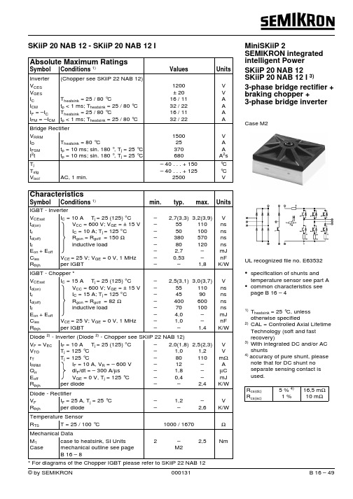
000131Absolute Maximum RatingsSymbol Conditions 1)ValuesUnitsInverter (Chopper see SKiiP 22 NAB 12)V CES V GES I C I CMI F = –I C I FM = –I CMT heatsink = 25 / 80 °Ct p < 1 ms; T heatsink = 25 / 80 °C T heatsink = 25 / 80 °Ct p < 1 ms; T heatsink = 25 / 80 °C1200± 2016 / 1132 / 2216 / 1132 / 22V V A A A A Bridge Rectifier V RRMI DI FSM I 2tT heatsink = 80 °C t p = 10 ms; sin. 180 °, T j = 25 °C t p = 10 ms; sin. 180 °, T j = 25 °C 150025370680V A A A 2s T j T stg V isol AC, 1 min.– 40 . . . + 150– 40 . . . + 1252500°C °C VSKiiP 20 NAB 12 - SKiiP 20 NAB 12 I MiniSKiiP 2SEMIKRON integrated intelligent Power SKiiP 20 NAB 12SKiiP 20 NAB 12 I 3)3-phase bridge rectifier +braking chopper +3-phase bridge inverterCase M2UL recognized file no. E63532•specification of shunts andtemperature sensor see part A •common characteristics see page B 16 – 41)T heatsink = 25 °C, unless otherwise specified2)CAL = Controlled Axial Lifetime Technology (soft and fast recovery)3)With integrated DC and/or AC shunts4) accuracy of pure shunt, please note that for DC shunt no separate sensing contact is used.R cs(dc)R cs(ac)5 % 4)1 %16,5 m Ω10 m Ω000131Fig. 3Turn-on /-off energy = f (I C )Fig. 4Turn-on /-off energy = f (R G )T j = 125 °C V CE = 600 V V GE = ± 15 V I C = 10 AT j = 125 °C V CE = 600 V V GE = ± 15 V R G = 150 ΩI Cpuls = 10 AV GE = 0 V f = 1 MHzFig. 1Typ. output characteristic, t p = 80 µs; 25 °CFig. 2Typ. output characteristic, t p = 80 µs; 125 °CFig. 5Typ. gate charge characteristic Fig. 6Typ. capacitances vs. V CE0698T j = ≤ 150 °C V GE = ± 15 V t sc = ≤ 10 µs L ext < 25 nHT j = ≤ 150 °C V GE = ± 15 VT j = 150 °C V GE = ≥ 15 VFig. 9Turn-off safe operating area (RBSOA) of the IGBT Fig. 10Safe operating area at short circuit of the IGBTFig. 7Rated current of the IGBT I Cop / I C = f (T h)00.20.40.60.81.01.2255075100125150I Cop /I C Mini1207T h [°C]00,511,522,550010001500I Cpuls /I C Mini1209V CE [V]02468101250010001500Note:*Allowed nu mbers of short ci r cuit:<1000*Time between short circuit:>1sI Csc /I CN Mini1210V CE [V]Fig. 11Typ. freewheeling diode forward characteristic Fig. 12Forward characteristic of the input bridge diode MiniSKiiP 1200 VMiniSKiiP 2SKiiP 20 NAB 06 ... SKiiP 21 NAB 06 ... SKiiP 20 NAB 12 ... SKiiP 22 NAB 12 ...CircuitCase M2Layout and connections for thecustomer’s printed circuit boardNote:The shunts are availableonly by option I-DC/AIsw0wIsv0v0uIsuI+B-TL3L1L2+rect-DC-rectg1UVW+T+DCg3g5g2g6g4gB+B-BHauptanschlußpower connectorcontrol pinSteueranschluß。
SKIIP23NAB126V1中文资料

1 (' 2/
! Values
*(44 8* 6&*7 '4 ; (4 = 84 ### > *'4
Units
, , 2 2 , @ 2 2 ,
Diode - Inverter, Chopper
MiniSKiiP 2 3-phase bridge rectifier + brake chopper + 3-phase bridge inverter
Fig. 8 Typ. thermal impedance
Fig. 9 Typ. freewheeling diode forward characteristic
Fig. 10 Typ. input bridge forward characteristic
3
02-05-2007 SCT
© by SEMIKRON
元器件交易网
SKiiP 23NAB126V1 CONVERTER, INVERTER, BRAKE
Absolute Maximum Ratings Symbol Conditions IGBT - Inverter, Chopper
,$3 9 ,$3 < 1 (' 6.47 2 ! : * -
Fig. 6 Typ. Turn-on /-off energy = f (RG)
2
02-05-2007 SCT
© by SEMIKRON
元器件交易网
SKiiP 23NAB126V1 CONVERTER, INVERTER, BRAKE
Fig. 7 Typ. gate charge characteristic
SKIIP642GB120-2D_07中文资料
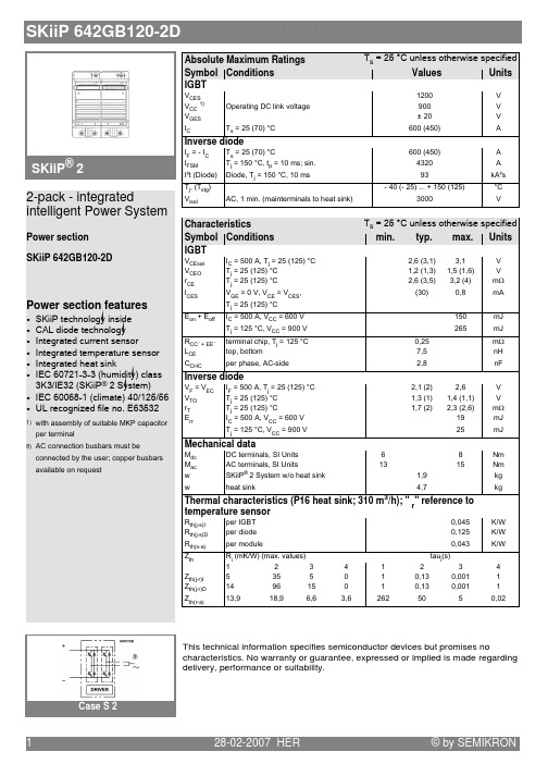
SKiiP 642GB120-2D INTEGRATED DRIVER, SENSORS
SKiiP® 2
2-pack - integrated intelligent Power System
Power section
SKiiP 642GB120-2D
Power section features
#"C%
:
+C
:
#
R
#C,
P
Hale Waihona Puke #C+P>
P
%C%
P
,
,
C
:
%
:
!,
##
#"
9
>
:
For electrical and thermal design support please use SEMISEL. Access to SEMISEL is via SEMIKRON website .
28-02-2007 HER
© by SEMIKRON
元器件交易网
SKiiP 642GB120-2D INTEGRATED DRIVER, SENSORS
SKiiP® 2
Absolute Maximum Ratings Symbol Conditions
:# :" :J
6
/
6
/ 8 4 0
(
7 8 ", 9
1
/
Values
Units
#*
:
- 1、下载文档前请自行甄别文档内容的完整性,平台不提供额外的编辑、内容补充、找答案等附加服务。
- 2、"仅部分预览"的文档,不可在线预览部分如存在完整性等问题,可反馈申请退款(可完整预览的文档不适用该条件!)。
- 3、如文档侵犯您的权益,请联系客服反馈,我们会尽快为您处理(人工客服工作时间:9:00-18:30)。
SSE
苏州迅达电梯有限公司
215004 苏州/中国
Skiip模块说明
技术培训中心编制:李志弘2003/05/13 A. 变频功率装置所用大功率晶体管的重要参数比较:
双极晶体管MOS IGBT 驱动方式电流电压电压
载波频率≤3KHz ≤60 KHz ≤20KHz 电流容量中低中
击穿电压中低高
短路安全工作区好好不好饱和电压高低中
综合特点1.电机啸叫噪音高
2.调制精度要求不高
3.输出容量小
4.截止频率低
5.抗短路性能好
1.输出容量小
2.输出电压、电流小
3.调制精度高
4.无噪音
5.截止频率高
1.输出容量大
2.输出电压、电流大
3.调制精度高
4.当载波频率≥
10.8KHz时,电机
无啸叫声。
5.功率因素可达1
6.抗短路性能差
B.变频器基本工作原理:
变频器工作基本原理如下:
a. 三相交流电源输入三相桥式整流器整流。
(将AC变为DC)
b. 整流后进入直流中间回路滤波。
(对DC进行滤波)
c. 滤波后的直流电进入逆变器(由六个IGBT组成)。
(再将DC逆变成频率、电压
可变的三相交流电)
d. 由驱动控制部分控制逆变器的导通和关断,把直流电压转换成新的频率和电
压均可调制的三相交流电源,U2,f2,于是电机就以设定速度n运行。
e. 驱动控制部分能形成闭环控制,同时监控整个系统。
f. 电机处于发电状态时(例如:电梯空载上行或重载下行的减速时)制动斩波器
工作,通过制动电阻R使多余能量消耗。
(也可采用逆变至送电电网)
电梯所用逆变器基本上都采用IGBT型场效应管作为开关管。
C.变频器主要特性分析:
1.变频器在逆变输出期间,其输出端的三相交流电压中包含着nfc(fc为载波频率,n= 1,2…)的高次谐波,而这种频率的谐波电压会使电机产生刺耳的噪音,通常采取的措施是增加载波频率使之大于10.8KHz,使电机共振啸叫噪音超出工频电源的频率,
从而保证频率在0~50Hz范围内变化时,电机无噪音。
但在增加载波频率的同时,会增加变频器周围电磁波的发射,导致周围的空间污染,这已经在欧、美国家引起高度重视和法律、法规的限制。
每增大1 KHz载波频率会使输出端增大1.2A 的额外附加电流,从而增加无谓的电能消耗。
综上所说,对于采用IGBT作为逆变功率管,其载波频率控制在11~12KHz之间为最佳,迅达变频器设定在11.9KHz,所有超出该范围的变频器会使设备的消耗能量增加。
2.通常采用IGBT的变频器其驱动控制部分是由微机按照逻辑控制的模式组成。
逻辑控制模块的功能是:根据时序控制原则(主要受控于设定时间),产生触发信号触发IGBT的控制极,控制IGBT的通断状态,从而控制逆变器IGBT输出交流电源的电压V、频率f,按照比值恒定和预先设定的输出曲线要求输出。
其缺点是:一旦时序控制出现误差,最容易使IGBT逆变功率管短路烧毁;其次,其调制参考参数由传统的理想参数、矢量变换、实际电流、实际速度组成,而缺少了电梯所特有的负载变化、运行方向变化和由电机温度变化而引发的电机参数的变化,从而最终影响电梯的舒适感和平层精度。
3.由此,迅达率先开发了符合现代电梯需要的新一代变频专用智能模块,专门针对由逻辑控制触发IGBT逆变器组成的变频器存在的缺点,研制了迅达电梯专用的SKIIP 智能模块。
它将IGBT的控制方式变为智能控制模式,调制参考参数不但包括了原有的理想参数、矢量变换、实际电流、实际速度,还包括了电梯因不同负载变化、运行方向变化和电机温度变化而引发的电机参数的变化等因素,运用强大的智能运算功能和预见模块,对驱动输出进行实时监控、纠正、调整、控制,根据该电梯当前实际负载、运行方向和速度的需要,使之实际驱动工况完全符合理想运行曲线设定的要求,不受任何因素影响而改变,保证每次运行效果达到理想状态和节能,并且包含了强大的电路短路安全保护系统、故障预先检查保护和故障自诊断功能。
4. SKiiP根据不同的功率输出设有三种型号,作为一独立部件,SKiiP模块可被单独更换。
D.SKIIP模块的组成:
每个SKIIP模块由以下部分组成:
⏹一个散热片
⏹一个三相不稳压整流桥
⏹一个智能模块,它由以下部分组成:
●三个带独立驱动的IGBT和故障检查电路
●IGBT和为制动斩波设计的泄流二极管。
●各自独立的智能驱动器模块及中间直流环电压控制器。
图: 3个IGBT(逆变器)、IGBT制动斩波器及驱动器E.Skiip模块变频器的简图组成:
下图绘出了变频器VF中重要组成部分的概况。