大学物理实验报告英文版
英文实验报告模板

Title:Investigation of [Experiment Name or Objective]Introduction:The purpose of this experiment is to [briefly state the objective of the experiment]. The experiment aims to explore [briefly mention the variables or phenomena being investigated]. This report will detail the experimental setup, procedure, results, and conclusions drawn from the data collected.Objective:To [restate the objective of the experiment in a clear and concise manner].Materials:- List all the materials used in the experiment, including equipment, chemicals, samples, and any other items.1. [Equipment Name] - [Model or Description]2. [Chemical Name] - [Concentration or Volume]3. [Sample Name] - [Quantity]4. [Other Materials] - [Description]Procedure:1. [Step 1: Describe the first step of the procedure in detail. Include all actions taken and any safety precautions.]2. [Step 2: Continue with the next step, ensuring all actions and observations are clearly described.]3. [Step 3: Proceed with the subsequent steps, maintaining the samelevel of detail and clarity.]4. [Step 4: Complete the procedure by detailing the final steps and any additional notes or observations.]Observations:- Record all observations made during the experiment, including any visual, auditory, or tactile information.- Include any measurements taken, data collected, and any other relevant information.Data Analysis:- Present the data collected in tables, graphs, or other appropriate formats.- Discuss the significance of the data and how it relates to the objective of the experiment.- Use statistical analysis where applicable, and explain the results.Results:- Summarize the findings of the experiment.- Compare the results with the expected outcomes or previous studies, if applicable.- Discuss any anomalies or unexpected results.Discussion:- Interpret the results in the context of the experiment's objective.- Explain any limitations of the experiment and how they may have influenced the results.- Compare the findings with those of other experiments or literature.- Discuss the implications of the results and their potential applications.Conclusion:- Restate the objective of the experiment.- Summarize the key findings and their significance.- State whether the objective was achieved and why or why not.- Suggest areas for further research or modifications to the experimental procedure.Appendix:- Include any additional information that supports the experiment report but is not essential to understanding the main points.1. [Table of raw data]2. [Graphs or charts]3. [Photographs or diagrams]4. [Additional calculations or analyses]References:- List all the sources cited in the report, following the appropriate citation style.1. Author, A. (Year). Title of the work. Journal Name, Volume(Issue), Page range.2. Book Title (Edition). Author, A. (Year of publication). Publisher.3. Website Name. (Date of access). URLAcknowledgments:- Acknowledge anyone who assisted with the experiment, provided equipment, or contributed to the research in any way.Author Information:- Name of the author(s)- Affiliation- Contact informationDate:- Date of submission or completion of the experiment---This template can be adapted to fit the specific requirements of the experiment and the educational institution. The length of the report should be tailored to the complexity of the experiment and the depth of the analysis required.。
最新物理实验报告(英文)

最新物理实验报告(英文)Abstract:This report presents the findings of a recent physics experiment conducted to investigate the effects of quantum entanglement on particle behavior at the subatomic level. Utilizing a sophisticated setup involving photon detectors and a vacuum chamber, the experiment aimed to quantify the degree of correlation between entangled particles and to test the limits of nonlocal communication.Introduction:Quantum entanglement is a phenomenon that lies at the heart of quantum physics, where the quantum states of two or more particles become interlinked such that the state of one particle instantaneously influences the state of the other, regardless of the distance separating them. This experiment was designed to further our understanding of this phenomenon and its implications for the fundamental principles of physics.Methods:The experiment was carried out in a controlled environment to minimize external interference. A pair of photons was generated and entangled using a nonlinear crystal. The photons were then separated and sent to two distinct detection stations. The detection process was synchronized, and the data collected included the time, position, and polarization state of each photon.Results:The results indicated a high degree of correlation between the entangled photons. Despite being separated by a significant distance, the photons exhibited a consistent pattern in their polarization states, suggesting a strong entanglement effect. The data also showed that the collapse of the quantum state upon measurement occurred simultaneously for both particles, supporting the theory of nonlocality.Discussion:The findings of this experiment contribute to the ongoing debate about the nature of quantum entanglement and its potential applications. The consistent correlations observed between the entangled particles provide strong evidence for the nonlocal properties of quantum mechanics. This has implications for the development of quantum computing and secure communication technologies.Conclusion:The experiment has successfully demonstrated the robustness of quantum entanglement and its potential for practical applications. Further research is needed to explore the broader implications of these findings and to refine the experimental techniques for probing the quantum realm.References:[1] Einstein, A., Podolsky, B., & Rosen, N. (1935). Can Quantum-Mechanical Description of Physical Reality Be Considered Complete? Physical Review, 47(8), 777-780.[2] Bell, J. S. (1964). On the Einstein Podolsky RosenParadox. Physics, 1(3), 195-200.[3] Aspect, A., Grangier, P., & Roger, G. (1982). Experimental Tests of Realistic Local Theories via Bell's Theorem. Physical Review Letters, 49(2), 91-94.。
英语作文描写物理实验报告

英语作文描写物理实验报告Physics Experiment Report。
Introduction。
The purpose of this experiment is to investigate the relationship between the force applied to a spring and the resulting extension of the spring. Hooke's Law states that the extension of a spring is proportional to the force applied to it, provided that the elastic limit of the spring is not exceeded.Materials。
The materials used in this experiment include a spring, a set of weights, a ruler, and a stand.Procedure。
First, we set up the stand and attached the spring toit. Then, we measured the length of the spring when it was not under any load. Next, we added weights to the spring in increments of 100 grams and measured the length of thespring after each weight was added. We continued adding weights until the spring reached its elastic limit. Finally, we recorded our data and analyzed the results.Results。
实验报告英文

实验报告英文Title: The Art of Conducting an Experimental ReportIntroduction:The process of conducting and reporting experiments is a crucial aspect of scientific research. It allows researchers to communicate their findings, contribute to the existing body of knowledge, and foster collaboration within the scientific community. In this article, we will explore the essential components and structure of an experimental report, highlighting the importance of clear and concise language, accurate data presentation, and logical organization.1. Abstract:The abstract serves as a concise summary of the entire experimental report. It should provide a brief overview of the research question, methodology, key findings, and conclusions. By reading the abstract, readers can quickly grasp the main points of the study and decide whether to delve deeper into the report. 2. Introduction:The introduction section sets the stage for the experiment by providing background information, stating the research question or hypothesis, and explaining the significance of the study. It should include relevant literature review, identifying any existing gaps in knowledge and explaining how the experiment aims to address them.3. Materials and Methods:This section details the materials used, the experimental design, and themethods employed to collect and analyze data. It should be presented in a clear and logical sequence, allowing other researchers to replicate the experiment. The inclusion of statistical analyses and any ethical considerations is also crucial.4. Results:The results section presents the findings of the experiment in a structured and objective manner. Data can be presented in the form of tables, graphs, or figures, accompanied by concise descriptions and appropriate statistical analyses. The focus should be on providing accurate and relevant information without interpretation or speculation.5. Discussion:In the discussion section, researchers interpret and analyze the results, comparing them with previous studies and addressing any limitations or unexpected outcomes. It is essential to provide logical explanations and support statements with evidence. This section also offers an opportunity to propose future research directions and potential implications of the findings.6. Conclusion:The conclusion section summarizes the main findings of the experiment, restates the research question or hypothesis, and discusses the overall significance of the study. It should be concise and provide closure to the report.7. References:The references section lists all the sources cited within the experimental report. It is crucial to follow a specific citation style, such as APA or MLA, to ensureconsistency and facilitate further research.8. Appendices:Appendices may be included to provide additional information that is not crucial to the main body of the report but may be useful for readers who want to delve deeper into the experiment. This can include raw data, calculations, or detailed descriptions of experimental procedures.Conclusion:Conducting an experimental report requires careful planning, meticulous execution, and effective communication skills. By following the structure outlined above and adhering to the principles of clarity, accuracy, and logical organization, researchers can effectively share their findings with the scientific community. The art of crafting an experimental report is not only a scientific endeavor but also a means to contribute to the collective knowledge and drive further advancements in various fields of study.。
Lab-report-物理实验报告(英文)
IntroductionCapacitor is widely used in a variety of fields as it can store electric energy, such as Filtering, resonant circuit and moving phase. Different capacitors have different abilities to store energy, which is due to the difference of capacitance. Capacitance is the ability of a capacitor to store charge in an electric field, it is also a measure of the amount of electric potential energy stored (or separated) for a given electric potential. This report is going to investigate the capacitance of a capacitor made from the experiment by using different DC methods. Before the capacitor made from the experiment is measured, three DC methods will be tested to verify whether these methods are efficient by measuring the capacitance of the known capacitor. In addition, after measuring the unknown capacitor, the whole capacitors will be connected in parallel and the total size of capacitance will be measured.Theory Capacitance can be found by using:dA C r ⨯⨯=εε0. This is for two flat plates. As for the formula, C is the capacitance of a capacitor, A is the area of flat plates, d is the distance between the two flat plates, 0ε is the permittivity of vacuum, r ε is the relative permittivity. Permittivity is constant of proportionality that relates the electric field in a material to the electric displacement in that material and relative permittivity is the ratio of the permittivity of a substance tothat of free space or vacuum. Different materials have different relative permittivity, the behind table includes the relative permittivity of some different material:Source: (The Engineering Tool Box, 2011.) When two capacitors are placed in series, the charge on each plate is of equalof charges on plate and V is the voltage across the capacitor). When ais the initial voltage adding on the capacitor, e is a constant and it is 2.718, R is resistance, C is capacitance and 0I is the initial current flowing through the capacitor). Analogously, when a capacitor is discharged, it flows RC t e V V -=0and RC t eI I -=0.MethodsApparatus :Power supply, leads, ruler, calipers, clips, known capacitor, aluminum foil,。
大学物理实验报告英文版--温度传感器

Physical Lab Report :Temperature SensorsWriter: No:This time in the lab, I come to do something about temperature sensors.Before the experiment, I know that temperature sensors are very widely used lab equipment.From the guide, I can find their outputs changes as a function of temperature.The most commonly used ones in the lab are Platinum resistors and semiconductor thermocouples.In this experiment, I will describe the working principle of Platinum thermo-resistors, Semi-conductor thermo-resistor, and PN diode temperature sensor, and make measurements with them in the lab.At the beginning, I use the ice water to get the reference point to zero degree is 2 degree.So, when I deal with the data, I have changed the temperature into correct ones already.1.Semi-conductor thermo-resistorWithin range, the resistanc-temperature relation is ⎪⎭⎫⎝⎛=T B A R T expIf we calibrate the resistance at a temperature T 0 to be R 0, we can rewrite this relation into⎪⎪⎭⎫⎝⎛-+=0011ln ln T T B R R TAfter I change the unit of temperature into K, I use computer to make a linear fit and get a graph as follows:The slope of the line is equal to 1555.6, it means B=1555.6 K.which is a little bit smaller than the reference.2.Platinum thermo-resistorsA platinum resistor has a temperature-resistance relation of ()201TB AT R R T ++=R/Ω 4000 37023473 3106 2868 2544 2303 2101 1744 1569 1343 1282 1212 1146 1089 118967 896 838 773 724 668 624 586 561 538 505T/C27 30 33 36 39 42 45 48 51 54 57 60 63 66 69 72 75 78 83 88 93 98U/ V 0.1150.11830.12120.12350.1260.12830.13030.13210.13410.13620.1380.13970.14130.1430.14460.14650.14790.14940.15160.15410.15620.1583T/C 14 11 8 5 2 0 -2 -4 -6 -7 -8U/V 0.1064 0.10570.10490.10440.10360.1030.10240.10180.10120.10080.1003From the graph ,I get the coefficient of x2 is B=2.8*10-7 o C-2,the coefficient of x is A=6*10-4 C-13.PN diode temperature sensorT/C 35 38 42 45 47 51 53 55 57 59 61 64 66 98 99 101 103U/V 0.470.4620.450.44140.43660.42460.42010.41380.40750.40170.39580.38840.38350.29610.29290.28840.283T/C 69 72 74 76 78 80 83 85 87 88 90 92 94 96 105 106 110Semiconductor diodes begin conducting electricity only if a certain threshold voltage or cut-in voltage is present in the forward direction.The voltage drop across a forward-biased diode varies only a little with the current, and is a function of temperature; this effect can be used as a temperature sensor.Within a given range of temperature, the resistance varies linearly with temperature.U=-0.0025T+0.5425, as the I=100μA,so,R=-25T+5424,the temperature is 25Error analysis:1.The temperature is tested indirectly, so the measured temperature is a little slower or higher than the correct one,If not precise, then our result of the coefficient is not that correct.2.The ice-water is made by human, even its temperature is near 0, however, there still exists some worry weather it is 0 degree.。
大学物理实验报告英文版--X光
Experiment report of X-rayPrinciple:When we speak of attenuation of x-rays, we mean the decrease in intensity that occurs when the radiation passes through matter. This attenuation is caused mainly by the two effects: scattering and absorption.Although absorption and attenuation are different physical phenomena, the transilluminated object is often referred to -inaccurately- as an absorber; this should more properly be termed an attenuator. However, this description will follow the traditional usage in some places and refer to absorbers instead of attenuators.The scattering of x-ray quanta at the atoms of the attenuator material causes a part of the radiation to change direction. This reduces the intensity in original direction. This scattering can be either elastic or entail an energy loss or shift in wavelength, i.e. Inelastic scattering.When x-ray hits a fluorescence material, it excites the material, making fluorescence lights. This is the principle of a fluorescence screen. When x-ray is used in imaging, the transmitted light will carry interior information of the object.A more sophisticated x-ray detector is the so-called Geiger-Muller counter, an instrument for detecting the presence of and measuring ionizing radiation such as the x-rays. It converts the intensity of the x-ray into counting rates. We will use such a device in our lab.Attenuation of x-rays:When passing through a material, x-ray can be attenuated by E&M interactions. For a slab of thickness x, the transmission (defined as the ratio of the transmittedradiation to the incoming), x=. µ is the attenuation coefficient, with a dimensionT eμ-of 1/distance. µis a character of the material, and it varies, for example, as a function of atomic number. We will study this dependence in this lab. Bragg Diffraction da 0Like normal lights, when x-ray transmit through material with regular optical pattern (e.g. lattice), diffraction will happen if the wavelength of the x-ray is close to the lattice space. Such diffraction on the crystal is the so-called Bragg Diffraction. If the lattice spacing is d, and the x-ray and the crystal surface forms an angle θ, the angle where maximum diffraction happens will satisfy2sin ,1,2,d n n θλ==where n is an integer and λ is the wavelength.Lab equipment:The equipment is an x-ray lab system made by Leybold Inc. A schematic is shown below. 监控区X 光管实验区B1B2B3B4B5A1A2A3A4此区内所有操作必须带上手套进行!!The x-ray is generated by an electron beam with controllable energy (via the potential) and current. The x-ray is going into the detection chamber to the right. There is a removableaperture which focuses the x-ray, a rotatable sample holder, and a rotatable G-M counter. At the right end of the wall, there is a fluorescence screen for imagine.Operation details of the device will be given by the manual. Basically, you need to set the high voltage (U) which determine the energy of the x-ray, the current (I), and the angle of the sample holder (target) or the detector. A knob can be used to make the adjustment on selected parameters. “Coupled” movement means one moves the target and the detector together, the former by an angle α, and the latter by an angle 2α. Make sure the lead glass window is closed before you turn on the high voltage.Attenuator (target)Left: aluminum attenuator mounted on a curved plate with thickness of 0,0.5,1.0,1.5,2.0,2.5, and 3mm. One can select different thickness by selecting angle.Right: attenuation of different materials, all with a thickness of 0.5 mm, including Polystyrene (average Z=6), Aluminum (13), Iron (26), Copper (29), Zirconium(40) andSilver(47).2.Install the aperture. Install the Zr foil onto the aperture. This is to filter out the Kαline. Squeeze the NaCl crystal onto the sample holder.In this part of the procedure we need to make sure that the X ray beam, the crystal surface and the detector is aligned. Use the following alignment procedure by the Bragg Diffraction, the process is omitted.data:The first peak appears when it ’s 7.5 degree.1. analysis:2sin ,1,2,d n n θλ== Then, 9102sin 20.5640210sin 7.5 1.4724101d n θλ--⨯⨯⨯︒===⨯ m. That is, the wavelength of X ray is 101.472410-⨯ m.2.Measure the X ray attenuation to different thickness:Install the Zr foil onto the aperture. Set HV=21 kV, I=0.05 mA, ∆β=0, ∆t=100 s.Hit target key. Change the angle sequentially to 0, 10, 20, 30, 40, 50, 60 degree (the thickness of the attenuation increase by 0.5mm each step).For each of this setting, hit “scan ” to take the data, and hit “replay ” to get the average rate.attenuation of different thicknessthickness(mm) 0.5 1 1.5 2 2.5 3 Data(1/s) 21.4 9.6 4.4 2.8 1.7 1Fit the rate as a function of thickness (with background subtraction) to get the attenuation coefficient.Fit the data in origin with exponential fit (mode = expdec1), through equation x=. We form the graph of 1/T and x.So, we get thatT eμ-Hence,So, the attenuation coefficient is110.263783.79097tμ===.Measure the X ray attenuation to materials with different atomic mass:a)Remove the Zr filter. Insert the curved attenuator holder B (different target) intothe annulus slot on the plastic mount. Set HV = 30 kV, I=1 mA, ∆β=0, ∆t=100 s. Hittarget key. Change the angle sequentially to 0, 10, 20, 30, 40, 50, 60 degree,each corresponding to a given material.b)For each of this setting, hit “scan” to take the data, and hit “replay” to getthe average rate.c)For the scan with Zr filter.attenuation of different Z, with ZrZ 6 13 26 29 40 47 Data(1/s) 9117.9 7627.4 72.9 7.7 108.9 14.4No exact rule can be found.Install the Zr filter. Repeat of Z number.The graph turns out:attenuation of different Z, without ZrZ 6 13 26 29 40 47Data(1/s) 9025.4 9027.8 8308.4 75.2 5.2 74.8Plot the rate as a function of Znumber.Also,no exact rule can be found.Conclusion:1.the wavelength of X ray is 10⨯m.1.472410-2.The rate has no exact relationship with Z.Error:Whether I check the background or not will have a influence on the wavelength. The light in the room will maybe influence the data I got. When I did the experiment with the light on, thus the light will be stronger.。
英语作文物理电学实验报告

英语作文物理电学实验报告Physics Experiment Report on Electric Circuits。
Introduction。
Electric circuits are important in our daily lives as they form the basis of all electrical devices. In this experiment, we investigated the behavior of electric circuits, including Ohm's law, Kirchhoff's laws, and the behavior of resistors in series and parallel.Materials。
Power supply。
Ammeter。
Voltmeter。
Resistors (varying values)。
Wires。
Breadboard。
Procedure。
1. Set up the circuit as shown in the diagram below, using a breadboard to connect the components.2. Measure the voltage across the resistor using the voltmeter and record the value.3. Measure the current flowing through the resistor using the ammeter and record the value.4. Repeat steps 2-3 for different values of resistors.5. Connect resistors in series and parallel and measure the voltage and current across each resistor.Results。
物理实验报告 英文

物理实验报告英文Title: Investigating the Behavior of Light: A Physics Experiment Report Introduction:In this report, we will discuss the experimental setup, procedure, and results of a physics experiment aimed at investigating the behavior of light. Light, as a fundamental entity, exhibits various phenomena that are crucial for understanding the nature of our universe. By conducting this experiment, we aimed to deepen our knowledge of light's properties and its interaction with different materials.Experimental Setup:The experiment was conducted in a controlled laboratory environment with the following equipment:1. Light Source: A laser beam was used as the primary light source. Its monochromatic nature ensured a consistent wavelength throughout the experiment.2. Optical Bench: An optical bench with adjustable components, such as lenses, mirrors, and prisms, was used to manipulate and direct the laser beam.3. Photodetector: A photodetector was employed to measure the intensity of the laser beam after passing through various materials or undergoing different optical processes.Procedure:1. Refraction: The first part of the experiment focused on investigating thephenomenon of refraction. A glass prism was placed on the optical bench, and the laser beam was directed towards it. By varying the angle of incidence, we observed the corresponding change in the angle of refraction. The intensity of the laser beam was measured using the photodetector at different angles.2. Diffraction: In the second part, we explored the phenomenon of diffraction. A diffraction grating was placed in the path of the laser beam. By rotating the grating, we observed the diffraction pattern formed on a screen placed at a specific distance from the grating. The intensity of the diffracted light was measured using the photodetector.3. Interference: The final part of the experiment focused on the interference of light waves. Two narrow slits were placed in the path of the laser beam, creating two coherent sources of light. A screen was placed at a specific distance from the slits, and the interference pattern was observed. The intensity of the interference pattern was measured using the photodetector.Results and Discussion:1. Refraction: As the angle of incidence increased, the angle of refraction also increased. This confirmed the relationship between the two angles predicted by Snell's law. The intensity of the laser beam decreased as the angle of refraction increased, indicating the loss of energy during the refraction process.2. Diffraction: By rotating the diffraction grating, we observed a series of bright and dark fringes on the screen. The distance between the fringes decreased as the grating rotation angle increased, indicating a smaller wavelength ofdiffracted light. The intensity of the laser beam varied at different angles, demonstrating the constructive and destructive interference of light waves.3. Interference: The interference pattern displayed alternating bright and dark fringes. The intensity of the bright fringes was higher, indicating constructive interference, while the dark fringes represented destructive interference. The distance between the fringes increased as the distance from the slits to the screen increased, confirming the relationship between fringe separation and wavelength.Conclusion:Through this experiment, we gained valuable insights into the behavior of light. We observed and analyzed the phenomena of refraction, diffraction, and interference, which are fundamental to the understanding of optics. The results obtained aligned with the theoretical predictions, reinforcing our understanding of light's properties and its interaction with various materials. Conducting experiments such as these allows us to bridge the gap between theoretical knowledge and practical applications, ultimately leading to advancements in the field of physics.。
大学物理实验报告 英文版
大学物理实验报告Ferroelectric Control of Spin PolarizationABSTRACTA current drawback of spintronics is the large power that is usually required for magnetic writing, in contrast with nanoelectronics, which relies on “zero-current,” gate-controlled operations. Efforts have been made to control the spin-relaxation rate, the Curie temperature, or the magnetic anisotropy with a gate voltage, but these effects are usually small and volatile. We used ferroelectric tunnel junctions with ferromagnetic electrodes to demonstrate local, large, and nonvolatile control of carrier spin polarization by electrically switching ferroelectric polarization. Our results represent a giant type of interfacial magnetoelectric coupling and suggest a low-power approach for spin-based information control.Controlling the spin degree of freedom by purely electrical means is currently an important challenge in spintronics (1, 2). Approaches based on spin-transfer torque (3) have proven very successful in controlling the direction of magnetization in a ferromagnetic layer, but they require the injection of high current densities. An ideal solution would rely on the application of an electric field across an insulator, as in existing nanoelectronics. Early experiments have demonstrated the volatile modulation of spin-based properties with a gate voltage applied through a dielectric. Notable examples include the gate control of the spin-orbit interaction in III-V quantum wells (4), the Curie temperature T C (5), or the magnetic anisotropy (6) in magnetic semiconductors with carrier-mediated exchange interactions; for example, (Ga,Mn)As or (In,Mn)As. Electric field–induced modifications of magnetic anisotropy at room temperature have also been reported recently in ultrathin Fe-based layers (7, 8).A nonvolatile extension of this approach involves replacing the gate dielectric by a ferroelectric and taking advantage of the hysteretic response of its order parameter (polarization) with an electric field. When combined with (Ga,Mn)As channels, forinstance, a remanent control of T C over a few kelvin was achieved through polarization-driven charge depletion/accumulation (9, 10), and the magnetic anisotropy was modified by the coupling of piezoelectricity and magnetostriction (11, 12). Indications of an electrical control of magnetization have also been provided in magnetoelectric heterostructures at room temperature (13–17).Recently, several theoretical studies have predicted that large variations of magnetic properties may occur at interfaces between ferroelectrics and high-T C ferromagnets such as Fe (18–20), Co2MnSi (21), or Fe3O4 (22). Changing the direction of the ferroelectric polarization has been predicted to influence not only the interfacial anisotropy and magnetization, but also the spin polarization. Spin polarization [i.e., the normalized difference in the density of states (DOS) of majority and minority spin carriers at the Fermi level (E F)] is typically the key parameter controlling the response of spintronics systems, epitomized by magnetic tunnel junctions in which the tunnel magnetoresistance (TMR) is related to the electrode spin polarization by the Jullière formula (23). These predictions suggest that the nonvolatile character of ferroelectrics at the heart of ferroelectric random access memory technology (24) may be exploited in spintronics devices such as magnetic random access memories or spin field-effect transistors (2). However, the nonvolatile electrical control of spin polarization has not yet been demonstrated.We address this issue experimentally by probing the spin polarization of electrons tunneling from an Fe electrode through ultrathin ferroelectric BaTiO3 (BTO) tunnel barriers (Fig. 1A). The BTO polarization can be electrically switched to point toward oraway from the Fe electrode. We used a half-metallic La0.67Sr0.33MnO3(LSMO) (25) bottom electrode as a spin detector in these artificial multiferroic tunnel junctions (26, 27). Magnetotransport experiments provide evidence for a large and reversible dependence of the TMR on ferroelectric polarization direction.Fig. 1(A) Sketch of the nanojunction defined by electrically controlled nanoindentation. A thin resist is spin-coated on the BTO(1 nm)/LSMO(30 nm) bilayer. The nanoindentation is performed with a conductive-tip atomic force microscope, and the resultingnano-hole is filled by sputter-depositing Au/CoO/Co/Fe. (B) (Top) PFM phase image of a BTO(1 nm)/LSMO(30 nm) bilayer after poling the BTO along 1-by-4–μm stripes with either a negative or positive (tip-LSMO) voltage. (Bottom) CTAFM image of an unpoled area of a BTO(1 nm)/LSMO(30 nm) bilayer. Ω, ohms. (C) X-ray absorption spectra collected at room temperature close to the Fe L3,2 (top), Ba M5,4 (middle), and TiL3,2 (bottom) edges on an AlO x(1.5 nm)/Al(1.5 nm)/Fe(2 nm)/BTO(1 nm)/LSMO(30 nm)//NGO(001) heterostructure. (D) HRTEM and (E) HAADF images of the Fe/BTO interface in a Ta(5 nm)/Fe(18 nm)/BTO(50 nm)/LSMO(30 nm)//NGO(001) heterostructure. The white arrowheads in (D) indicate the lattice fringes of {011} planes in the iron layer. [110] and [001] indicate pseudotetragonal crystallographic axes of the BTO perovskite.The tunnel junctions that we used in this study are based on BTO(1 nm)/LSMO(30 nm) bilayers grown epitaxially onto (001)-oriented NdGaO3 (NGO) single-crystal substrates (28). The large (~180°) and stable piezoresponse force microscopy (PFM) phase contrast (28) between negatively and positively poled areas (Fig. 1B, top) indicates that the ultrathin BTO films are ferroelectric at room temperature (29). The persistence of ferroelectricity for such ultrathin films of BTO arises from the large lattice mismatch with the NGO substrate (–3.2%), which is expected to dramatically enhance ferroelectric properties in this highly strained BTO (30). The local topographical and transport properties of the BTO(1 nm)/LSMO(30 nm) bilayers were characterized by conductive-tip atomic force microscopy (CTAFM) (28). The surface is very smooth with terraces separated by one-unit-cell–high steps, visible in both the topography (29) and resistance mappings (Fig. 1B, bottom). No anomalies in the CTAFM data were observed over lateral distances on the micrometer scale.We defined tunnel junctions from these bilayers by a lithographic technique based on CTAFM (28, 31). Top electrical contacts of diameter ~10 to 30 nm can be patterned by this nanofabrication process. The subsequent sputter deposition of a 5-nm-thick Fe layer, capped by a Au(100 nm)/CoO(3.5 nm)/Co(11.5 nm) stack to increase coercivity, defined a set of nanojunctions (Fig. 1A). The same Au/CoO/Co/Fe stack was deposited on another BTO(1 nm)/LSMO(30 nm) sample for magnetic measurements. Additionally, a Ta(5 nm)/Fe(18 nm)/BTO(50 nm)/LSMO(30 nm) sample and a AlO x(1.5 nm)/Al(1.5nm)/Fe(2 nm)/BTO(1 nm)/LSMO(30 nm) sample were realized for structural and spectroscopic characterizations.We used both a conventional high-resolution transmission electron microscope (HRTEM) and the NION UltraSTEM 100 scanning transmission electron microscope (STEM) to investigate the Fe/BTO interface properties of the Ta/Fe/BTO/LSMO sample. The epitaxial growth of the BTO/LSMO bilayer on the NGO substrate was confirmed by HRTEM and high-resolution STEM images. The low-resolution, high-angle annular dark field (HAADF) image of the entire heterostructure shows the sharpness of theLSMO/BTO interface over the studied area (Fig. 1E, top). Figure 1D reveals a smooth interface between the BTO and the Fe layers. Whereas the BTO film is epitaxially grown on top of LSMO, the Fe layer consists of textured nanocrystallites. From the in-plane (a) and out-of-plane (c) lattice parameters in the tetragonal BTO layer, we infer that c/a = 1.016 ± 0.008, in good agreement with the value of 1.013 found with the use of x-ray diffraction (29). The interplanar distances for selected crystallites in the Fe layer [i.e.,~2.03 Å (Fig. 1D, white arrowheads)] are consistent with the {011} planes ofbody-centered cubic (bcc) Fe.We investigated the BTO/Fe interface region more closely in the HAADF mode of the STEM (Fig. 1E, bottom). On the BTO side, the atomically resolved HAADF image allows the distinction of atomic columns where the perovskite A-site atoms (Ba) appear as brighter spots. Lattice fringes with the characteristic {100} interplanar distances of bcc Fe (~2.86 Å) can be distinguished on the opposite side. Subtle structural, chemical, and/or electronic modifications may be expected to occur at the interfacial boundarybetween the BTO perovskite-type structure and the Fe layer. These effects may lead to interdiffusion of Fe, Ba, and O atoms over less than 1 nm, or the local modification of the Fe DOS close to E F, consistent with ab initio calculations of the BTO/Fe interface (18–20).To characterize the oxidation state of Fe, we performed x-ray absorption spectroscopy (XAS) measurements on a AlO x(1.5 nm)/Al(1.5 nm)/Fe(2 nm)/BTO(1 nm)/LSMO(30 nm) sample (28). The probe depth was at least 7 nm, as indicated by the finite XAS intensity at the La M4,5 edge (28), so that the entire Fe thickness contributed substantially to the signal. As shown in Fig. 1C (top), the spectrum at the Fe L2,3 edge corresponds to that of metallic Fe (32). The XAS spectrum obtained at the Ba M4,5 edge (Fig. 1C, middle) is similar to that reported for Ba2+ in (33). Despite the poor signal-to-noise ratio, the Ti L2,3 edge spectrum (Fig. C, bottom) shows the typical signature expected for a valence close to 4+ (34). From the XAS, HRTEM, and STEM analyses, we conclude that theFe/BTO interface is smooth with no detectable oxidation of the Fe layer within a limit of less than 1 nm.After cooling in a magnetic field of 5 kOe aligned along the [110] easy axis of pseudocubic LSMO (which is parallel to the orthorhombic [100] axis of NGO), we characterized the transport properties of the junctions at low temperature (4.2K). Figure 2A (middle) shows a typical resistance–versus–magnetic field R(H) cycle recorded at a bias voltage of –2 mV (positive bias corresponds to electrons tunneling from Fe to LSMO). The bottom panel of Fig. 2A shows the magnetic hysteresisloop m(H) of a similar unpatterned sample measured with superconducting quantuminterference device (SQUID) magnetometry. When we decreased the magnetic field from a large positive value, the resistance dropped in the –50 to –250 Oe range and then followed a plateau down to –800 Oe, after which it sharply returned to thehigh-resistance state. We observed a similar response when cycling the field back to large positive values. A comparison with the m(H) loop indicates that the switching fields in R(H) correspond to changes in the relative magnetic configuration of the LSMO and Fe electrodes from parallel (at high field) to antiparallel (at low field). The magnetically softer LSMO layer switched at lower fields (50 to 250 Oe) compared with the Fe layer, for which coupling to the exchange-biased Co/CoO induces larger and asymmetric coercive fields (–800 Oe, 300 Oe). The observed R(H) corresponds to a negative TMR = (R ap–R p)/R ap of –17% [R p and R ap are the resistance in the parallel (p) and antiparallel (ap) magnetic configurations, respectively; see the sketches in Fig. 2A]. Within the simple Jullière model of TMR (23) and considering the large positive spin polarization of half-metallic LSMO (25), this negative TMR corresponds to a negative spin polarization for bcc Fe at the interface with BTO, in agreement with ab initio calculations (18–20).Fig. 2(A) (Top) Device schematic with black arrows to indicate magnetizations. p, parallel; ap, antiparallel. (Middle) R(H) recorded at –2 mV and 4.2 K showing negative TMR. (Bottom) m(H) recorded at 30 K with a SQUID magnetometer. emu, electromagnetic units. (B) (Top) Device schematic with arrows to indicate ferroelectric polarization. (Bottom) I(V DC) curves recorded at 4.2 K after poling the ferroelectric down (orange curve) or up (brown curve). The bias dependence of the TER is shown in the inset.As predicted (35–38) and demonstrated (29) previously, the tunnel current across a ferroelectric barrier depends on the direction of the ferroelectric polarization. We also observed this effect in our Fe/BTO/LSMO junctions. As can be seen in Fig. 2B, after poling the BTO at 4.2 K to orient its polarization toward LSMO or Fe (with a poling voltage of VP–≈ –1 V or VP+≈ 1 V, respectively; see Fig. 2B sketches),current-versus-voltage I(V DC) curves collected at low bias voltages showed a finite difference corresponding to a tunnel electroresistance as large as TER = (I VP+–I VP–)/I VP–≈ 37% (Fig. 2B, inset). This TER can be interpreted within an electrostatic model (36–39), taking into account the asymmetric deformation of the barrier potential profile that is created by the incomplete screening of polarization charges by different Thomas-Fermi screening lengths at Fe/BTO and LSMO/BTO interfaces.Piezoelectric-related TER effects (35, 38) can be neglected as the piezoelectric coefficient estimated from PFM experiments is too small in our clamped films (29). TER measurements performed on a BTO(1 nm)/LSMO(30 nm) bilayer with the use of a CTAFM boron-doped diamond tip as the top electrode showed values of ~200%(29). Given the strong sensitivity of the TER on barrier parameters and barrier-electrode interfaces, these two values are not expected to match precisely. We anticipate that the TER variation between Fe/BTO/LSMO junctions and CTAFM-based measurements is primarily the result of different electrostatic boundary conditions.Switching the ferroelectric polarization of a tunnel barrier with voltage pulses is also expected to affect the spin-dependent DOS of electrodes at a ferromagnet/ferroelectric interface. Interfacial modifications of the spin-dependent DOS of the half-metallic LSMO by the ferroelectric BTO are not likely, as no states are present for the minority spins up to ~350 meV above E F (40, 41). For 3d ferromagnets such as Fe, large modifications of the spin-dependent DOS are expected, as charge transfer between spin-polarized empty and filled states is possible. For the Fe/BTO interface, large changes have been predicted through ab initio calculations of 3d electronic states of bcc Fe at the interface with BTO by several groups (18–20).To experimentally probe possible changes in the spin polarization of the Fe/BTO interface, we measured R(H) at a fixed bias voltage of –50 mV after aligning the ferroelectric polarization of BTO toward Fe or LSMO. R(H) cycles were collected for each direction of the ferroelectric polarization for two typical tunnel junctions of the same sample (Fig. 3, B and C, for junction #1; Fig. 3, D and E, for junction #2). In both junctions at the saturating magnetic field, high- and low-resistance states are observed when the ferroelectric polarization points toward LSMO or Fe, respectively, with a variation of ~ 25%. This result confirms the TER observations in Fig. 2B.Fig. 3(A) Sketch of the electrical control of spin polarization at the Fe/BTO interface.(B and C) R(H) curves for junction #1 (V DC = –50 mV, T = 4.2 K) after poling the ferroelectric barrier down or up, respectively. (D and E) R(H) curves for junction #2 (V DC = –50 mV, T= 4.2 K) after poling the ferroelectric barrier down or up, respectively.More interestingly, here, the TMR is dramatically modified by the reversal of BTO polarization. For junction #1, the TMR amplitude changes from –17 to –3% when the ferroelectric polarization is aligned toward Fe or LSMO, respectively (Fig. 3, B and C). Similarly for junction #2, the TMR changes from –45 to –19%. Similar results were obtained on Fe/BTO (1.2 nm)/LSMO junctions (28). Within the Jullière model (23), these changes in TMR correspond to a large (or small) spin polarization at the Fe/BTO interface when the ferroelectric polarization of BTO points toward (or away from) the Fe electrode. These experimental data support our interpretation regarding the electrical manipulation of the spin polarization of the Fe/BTO interface by switching the ferroelectric polarization of the tunnel barrier.To quantify the sensitivity of the TMR with the ferroelectric polarization, we define a term, the tunnel electromagnetoresistance, as TEMR = (TMR VP+–TMR VP–)/TMR VP–. Largevalues for the TEMR are found for junctions #1 (450%) and #2 (140%), respectively. This electrical control of the TMR with the ferroelectric polarization is repeatable, as shown in Fig. 4 for junction #1 where TMR curves are recorded after poling the ferroelectric up, down, up, and down, sequentially (28).Fig. 4TMR(H) curves recorded for junction #1 (V DC = –50 mV, T = 4.2 K) after poling the ferroelectric up (VP+), down (VP–), up (VP+), and down (VP–).For tunnel junctions with a ferroelectric barrier and dissimilar ferromagnetic electrodes, we have reported the influence of the electrically controlled ferroelectric barrier polarization on the tunnel-current spin polarization. This electrical influence over magnetic degrees of freedom represents a new and interfacial magnetoelectric effect that is large because spin-dependent tunneling is very sensitive to interfacial details. Ferroelectrics can provide a local, reversible, nonvolatile, and potentially low-power means of electrically addressing spintronics devices.Supporting Online Material/cgi/content/full/science.1184028/DC1Materials and MethodsFigs. S1 to S5References∙Received for publication 30 October 2009.∙Accepted for publication 4 January 2010.References and Notes1. C. Chappert, A. Fert, F. N. Van Dau, The emergence of spin electronics indata storage. Nat. Mater. 6,813 (2007).2.I. Žutić, J. Fabian, S. Das Sarma, Spintronics: Fundamentals andapplications. Rev. Mod. Phys. 76,323 (2004).3.J. C. Slonczewski, Current-driven excitation of magnetic multilayers. J.Magn. Magn. Mater. 159, L1(1996).4.J. Nitta, T. Akazaki, H. Takayanagi, T. Enoki, Gate control of spin-orbit interaction in an inverted In0.53Ga0.47As/In0.52Al0.48Asheterostructure. Phys. Rev. Lett. 78, 1335 (1997).5.H. Ohno et al., Electric-field control offerromagnetism. Nature 408, 944 (2000).6. D. Chiba et al., Magnetization vector manipulation by electricfields. Nature 455, 515 (2008).7.M. Weisheit et al., Electric field–induced modification of magnetism inthin-film ferromagnets. Science315, 349 (2007).8.T. Maruyama et al., Large voltage-induced magnetic anisotropy changein a few atomic layers of iron.Nat. Nanotechnol. 4, 158 2009).9.S. W. E. Riester et al., Toward a low-voltage multiferroic transistor:Magnetic (Ga,Mn)As under ferroelectric control. Appl. Phys.Lett. 94, 063504 (2009).10.I. Stolichnov et al., Non-volatile ferroelectric control of ferromagnetismin (Ga,Mn)As. Nat. Mater. 7, 464(2008).11. C. Bihler et al., Ga1−x Mn x As/piezoelectric actuator hybrids: A modelsystem for magnetoelastic magnetization manipulation. Phys. Rev.B 78, 045203 (2008).12.M. Overby, A. Chernyshov, L. P. Rokhinson, X. Liu, J. K. Furdyna, GaMnAs-based hybrid multiferroic memory device. Appl. Phys.Lett. 92, 192501 (2008).13. C. Thiele, K. Dörr, O. Bilani, J. Rödel, L. Schultz, Influence of strain on themagnetization and magnetoelectric effect inLa0.7A0.3MnO3∕PMN-PT(001)(A=Sr,Ca). Phys.Rev.B 75, 054408 (2007).14.W. Eerenstein, M. Wiora, J. L. Prieto, J. F. Scott, N. D. Mathur, Giantsharp and persistent converse magnetoelectric effects in multiferroic epitaxial heterostructures. Nat. Mater. 6, 348 (2007).15.T. Kanki, H. Tanaka, T. Kawai, Electric control of room temperatureferromagnetism in a Pb(Zr0.2Ti0.8)O3/La0.85Ba0.15MnO3 field-effect transistor. Appl.Phys. Lett. 89, 242506 (2006).16.Y.-H. Chu et al., Electric-field control of local ferromagnetism using amagnetoelectric multiferroic. Nat. Mater. 7, 478 2008).17.S. Sahoo et al., Ferroelectric control of magnetism in BaTiO3∕Feheterostructures via interface strain coupling. Phys. Rev. B 76, 092108 (2007). 18. C.-G. Duan, S. S. Jaswal, E. Y. Tsymbal, Predicted magnetoelectric effectin Fe/BaTiO3 multilayers: Ferroelectric control of magnetism. Phys. Rev.Lett. 97, 047201 (2006).19.M. Fechner et al., Magnetic phase transition in two-phase multiferroicspredicted from first principles.Phys. Rev. B 78, 212406 (2008).20.J. Lee, N. Sai, T. Cai, Q. Niu, A. A. Demkov, preprint availableat /abs/0912.3492v1.21.K. Yamauchi, B. Sanyal, S. Picozzi, Interface effects at ahalf-metal/ferroelectric junction. Appl. Phys. Lett. 91, 062506 (2007).22.M. K. Niranjan, J. P. Velev, C.-G. Duan, S. S. Jaswal, E. Y. Tsymbal, Magnetoelectric effect at the Fe3O4/BaTiO3 (001) interface: A first-principles study. Phys. Rev. B 78, 104405 (2008).23.M. Jullière, Tunneling between ferromagnetic films. Phys. Lett.A 54, 225 (1975).24.J. F. Scott, Applications of modern ferroelectrics. Science 315, 954 (2007).25.M. Bowen et al., Nearly total spin polarization in La2/3Sr1/3MnO3 fromtunneling experiments. Appl. Phys. Lett. 82, 233 (2003).26.J. P. Velev et al., Magnetic tunnel junctions with ferroelectric barriers:Prediction of four resistance states from first principles. Nano Lett. 9, 427 (2009).27. F. Yang et al., Eight logic states of tunneling magnetoelectroresistancein multiferroic tunnel junctions.J. Appl. Phys. 102, 044504 (2007).28.Materials and methods are available as supporting materialon Science Online.29.V. Garcia et al., Giant tunnel electroresistance for non-destructivereadout of ferroelectric states. Nature460, 81 (2009).30.K. J. Choi et al., Enhancement of ferroelectricity in strained BaTiO3 thinfilms. Science 306, 1005(2004).31.K. Bouzehouane et al., Nanolithography based on real-time electricallycontrolled indentation with an atomic force microscope for nanocontactelaboration. Nano Lett. 3, 1599 (2003).32.T. J. Regan et al., Chemical effects at metal/oxide interfaces studied byx-ray-absorption spectroscopy.Phys. Rev. B 64, 214422 (2001).33.N. Hollmann et al., Electronic and magnetic properties of the kagomesystems YBaCo4O7 and YBaCo3M O7 (M=Al, Fe). Phys. Rev. B 80, 085111 (2009).34.M. Abbate et al., Soft-x-ray-absorption studies of the location of extracharges induced by substitution in controlled-valence materials. Phys. Rev.B 44, 5419 (1991).35. E. Y. Tsymbal, H. Kohlstedt, Tunneling across aferroelectric. Science 313, 181 (2006).36.M. Ye. Zhuravlev, R. F. Sabirianov, S. S. Jaswal, E. Y. Tsymbal, Giantelectroresistance in ferroelectric tunnel junctions. Phys. Rev.Lett. 94, 246802 (2005).37.M. Ye. Zhuravlev, R. F. Sabirianov, S. S. Jaswal, E. Y. Tsymbal, Erratum:Giant electroresistance in ferroelectric tunnel junctions. Phys. Rev.Lett. 102, 169901 2009).38.H. Kohlstedt, N. A. Pertsev, J. Rodriguez Contreras, R. Waser, Theoreticalcurrent-voltage characteristics of ferroelectric tunnel junctions. Phys. Rev.B 72, 125341 (2005).39.M. Gajek et al., Tunnel junctions with multiferroic barriers. Nat.Mater. 6, 296 (2007).40.M. Bowen et al., Spin-polarized tunneling spectroscopy in tunneljunctions with half-metallic electrodes.Phys. Rev. Lett. 95, 137203 (2005).41.J. D. Burton, E. Y. Tsymbal, Prediction of electrically induced magneticreconstruction at the manganite/ferroelectric interface. Phys. Rev.B 80, 174406 (2009).42.We thank R. Guillemet, C. Israel, M. E. Vickers, R. Mattana, J.-M. George,and P. Seneor for technical assistance, and C. Colliex for fruitful discussions on the microscopy measurements. This study was partially supported by theFrance-U.K. Partenariat Hubert Curien Alliance program, the French RéseauThématique de Recherche Avancée Triangle de la Physique, the European Union (EU) Specific Targeted Research Project (STRep) Manipulating the Coupling inMultiferroic Films, EU STReP Controlling Mesoscopic Phase Separation, U.K. Engineering and Physical Sciences Research Council grant EP/E026206/I, French C-Nano Île de France, French Agence Nationale de la Recherche (ANR) Oxitronics, French ANR Alicante, the European Enabling Science and Technology through European Elelctron Microscopy program, and the French Microscopie Electronique et Sonde Atomique network. X.M.acknowledges support from Comissionat per a Universitats i Recerca (Generalitat de Catalunya).。
大学英文物理实验报告(简易)

“Simple Harmonic Motion Experiment”AbstractIn this lab we are using spring weights, rod, clamp, string force sensor and rule to determine the spring constant using two different methods.Experiment DescriptionBefore starting the experiment, we need to calculate the spring constant k by using:F = -kxWhich F is force that pull or push the force sensor, x is displacement while weights are hanging on the spring. If the spring we use obey Hooke’s law, displacement(x) will follow the equation:x = A cos(ωt+Φ) (1)While A is the amplitude of oscillation,ω is the angular frequency in rad/s, Φ is the staring angle and t reference time in second. For both Φ and ω, we can use the following equations:ω = (k/m)^(1/2) (2)T = 2π[(m/k)^(1/2)] (3)For the first part of the experiment, we hang a mass holder from the end of the spring and measure the displacement from this point. Starting to add masses on the hanger from mass = 0.15kg. Measure the length changing and add additional 0.1kg at the end of the spring. Repeat 6 times and record the data to a excel table.For the second part, set up the computer and Data studio, open a graph reference force vs time. Set rate to 50Hz. Bump the weight in order to fit the graph like a sine wave, using fit area to find the period T. Repeat adding mass on the spring by 0.1kg each time. By squaring both side of (3), we have:T^2 = (4π^2)m/kPlot T^2 versus m to a excel form. Using linear equation to determine the slope k.Experiment ResultPart 1,Force vs. DisplacementPart 2, T^2 vs. Mass2.Value k found in Part 2: 29.03.3.Percentage difference: 0.24%.4.While y axis, which T^2 is 0, Mass actually is not 0. Because spring has mass on it andwill affect the total mass. Also, Air resistance will also being a fact.5.While on the moon, mass will also about 1/6 like on Earth. so the displacement willshorter. Because of no air resistance acting on the experiment, Part 2 may become more accurately.ConclusionThe experiment tell me about the constant resilience of a object. The force acts on this object will appears shape changes, which will follow F=-kx. By using two different ways to evaluate the constant k of the spring, we also know that we c an’t over extend object because there is a limit. While in the limitation, force and displacement will follow the Hooke’s law. After the force exceed over the limit, rule will break.。
物理实验报告英文

物理实验报告英文Title: Investigating the Effects of Temperature on the Viscosity of Liquids Introduction:In this experiment, we aim to explore the relationship between temperature and the viscosity of liquids. Viscosity refers to a fluid's resistance to flow, and it plays a crucial role in various fields, including chemical engineering, medicine, and geology. Understanding how temperature affects viscosity can provide valuable insights into the behavior of different liquids and their applications in various industries.Experimental Setup:To conduct this experiment, we used a viscometer, a device specifically designed to measure the viscosity of liquids. The viscometer consists of a cylindrical container with a small opening at the bottom and a stopwatch to measure the time it takes for a certain volume of liquid to flow through the opening. We selected three different liquids for our experiment: water, vegetable oil, and glycerin.Procedure:1. We started by setting up the viscometer and ensuring it was clean and free from any residue.2. We filled the viscometer with water and allowed it to reach room temperature.3. Using the stopwatch, we measured the time it took for a fixed volume of water to flow through the opening.4. We repeated the process three times and calculated the average time.5. Next, we heated the water to a specific temperature using a water bath.6. Again, we measured the time it took for the water to flow through the viscometer at the elevated temperature.7. We repeated steps 5 and 6 for different temperatures, ranging from room temperature to 80°C.8. Finally, we repeated the entire process using vegetable oil and glycerin, following the same temperature range.Results and Analysis:Upon analyzing the data obtained from the experiment, we observed a clear trend between temperature and viscosity for all three liquids. As the temperature increased, the viscosity of the liquids decreased. This phenomenon can be explained by the kinetic theory of matter, which states that as temperature increases, the kinetic energy of the molecules also increases. Consequently, the intermolecular forces holding the liquid together weaken, allowing the molecules to move more freely, resulting in reduced viscosity.Additionally, we found that the rate of viscosity decrease varied among the liquids. Water exhibited the most significant change in viscosity with temperature, followed by vegetable oil and glycerin. This difference can be attributed to the molecular structure and composition of each liquid. Water, being a polar molecule, experiences stronger intermolecular forces, leading to a more significant decrease in viscosity with increasing temperature.Conclusion:In conclusion, our experiment successfully demonstrated the relationship between temperature and the viscosity of liquids. The results indicate that as temperature increases, the viscosity of liquids decreases due to the weakening of intermolecular forces. This knowledge has practical applications in various industries, such as the design of lubricants, the optimization of chemical reactions, and the understanding of fluid dynamics. Further studies can explore the effects of pressure, concentration, and other factors on viscosity to deepen our understanding of fluid behavior.。
英文的物理实验报告

英文的物理实验报告英文的物理实验报告IntroductionIn the field of science, conducting experiments and documenting the results is an essential part of the research process. This holds true for physics as well, where experimental reports play a crucial role in presenting and analyzing the findings. In this article, we will explore the structure and content of an English physics experiment report, highlighting its importance and providing tips for effective writing.Experimental SetupThe first section of a physics experiment report typically outlines the experimental setup. Here, the writer describes the apparatus used, including any instruments, equipment, and materials. It is essential to provide sufficient details so that readers can understand and replicate the experiment if needed. Clear and concise language should be used to ensure accuracy and avoid any ambiguity.MethodologyThe methodology section explains the step-by-step procedure followed during the experiment. It should be written in a logical and sequential manner, allowing readers to understand the experimental process easily. It is advisable to use active voice and past tense when describing the actions performed during the experiment. Additionally, any calculations or formulas used should be clearlystated, ensuring transparency and reproducibility.Data Collection and AnalysisAfter conducting the experiment, the next step is to collect and analyze the data obtained. In this section, the writer presents the raw data gathered during the experiment. This can be done using tables, graphs, or charts, depending on the nature of the data. It is important to label and title all figures appropriately, providing units of measurement and clear legends.Once the data is presented, the analysis begins. The writer interprets the data, looking for patterns, trends, and relationships. Statistical methods, such as calculating averages or standard deviations, may be employed to support the analysis. It is crucial to provide a clear and logical explanation of the findings, relating them back to the objectives of the experiment.DiscussionThe discussion section is where the writer provides a deeper analysis of the results obtained. This is an opportunity to compare the findings with existing theories or prior research. Any discrepancies or unexpected outcomes should be addressed and explained. The writer may also suggest possible sources of error or limitations of the experiment, demonstrating a critical understanding of the experimental process.ConclusionThe conclusion summarizes the key findings of the experiment and their implications. It should be concise and to the point, highlighting the significanceof the results. The writer may also mention any recommendations for further research or improvements to the experimental setup. It is important to avoid introducing any new information in the conclusion, as it should serve as a summary of the report.ReferencesIn scientific writing, it is crucial to acknowledge the sources of information used. The references section provides a list of all the references cited in the report. The writer should follow a specific citation style, such as APA or MLA, and provide complete and accurate information for each reference. This ensures credibility and allows readers to explore the sources further if desired.ConclusionWriting an English physics experiment report requires careful attention to detail and a clear understanding of the scientific method. By following the structure outlined above and focusing on clarity and accuracy, researchers can effectively communicate their experimental findings. Experiment reports serve as a valuable tool for the scientific community, facilitating knowledge sharing and promoting further research and discovery.。
大学物理波动光学英文实验报告

Diffraction grating modeling by RCWA and CM methods: diffraction efficiency synchronism studiesIvan Richter,Petr Honsa,and Pavel FialaCzech Technical University in Prague,Faculty of Nuclear Sciences and Physical EngineeringDepartment of Physical Electronics,Břehová7,11519Prague l,CZECH REPUBLICPhone:+420221912285,Fax:+42026884818,Email:richter@troja.fjfi.cvut.czAbstract:This contribution concentrates on modeling of diffraction processes in opticaldiffraction gratings(ODG).First,the approach to characterization of mechanisms and diffractionprocesses is briefly presented,together with the regions with typical diffraction regimes.Differenttypes of diffraction efficiency volume phase synchronism are then described.Different situationsare analyzed and compared concerning ODG of different types,different refractive index/reliefmodulation profiles,various modulation strengths,and incident wave polarization influence.Asexamples,the cases of conical and Littrow mounts are discussed in detail.As rigorous modelingtools,both rigorous coupled wave analysis,and coordinate transformation methods are used,implemented,and modified.2002Optical Society of AmericaOCIS codes:050.1950Diffraction gratings,050.1970Diffractive optics1.Introduction and modeling toolsIn the last years,diffractive optics modeling,i.e.both analysis(direct problem)and synthesis(inverse problem)in diffractive optics has obtained an immense attention and interest,especially due to an increasing amount of practical applications of optical diffraction gratings(ODG)and diffractive optical elements and systems.Technological possibilities of grating fabrication methods to produce e.g.high-aspect ratio diffractive structures with periods(or minimum feature sizes)comparable and smaller than the wavelength of light have also enlarged rapidly.Hence, originally-used scalar theoretical methods(analytical methods of transmittance,two wave Kogelnik's methods,thin film decomposition,etc.)became inapplicable soon,and the rigorous methods had to start their developments and beings.Apart from design,fabrication and application driven rigorous modeling,diffraction processes characterization in ODG is also important itself since it can provide a deep insight into the physical mechanisms,can separate and identify their influences,and allows to find some regions(of important parameters)with typical diffraction regimes.In this sense,it is very useful and needful for all other types of modeling.Therefore,based on our previous studies[1-8],the purpose of this contribution is mainly to present,discuss and interpret on various examples new and physically interesting results concerning the behavior of the diffraction efficiency synchronism for selected grating and experimental parameters of diffraction gratings.As rigorous modeling tools,both rigorous coupled wave analysis(RCWA)and coordinate transformation methods(CM)have been implemented and applied within this contribution.RCWA,as a standard technique for the analysis of diffraction grating properties,nowadays represents an efficient and stable modelling tool[9].Our RCWA model has implemented several modifications and improvements,and was successfully applied in our previous studies[10].The coordinate transformation method has also shown a great potential in rigorous diffraction modelling,and become a strong counterpart of RCWA methods,efficiently applicable especially to specific types of surface-relief gratings[11].This method is based on the introduction of a new coordinate system transforming a generally complicated grating surface corrugation into a simple plane surface,hence simplifying the boundary-matching problem by a great extent.Our CM model,based mainly on the Li's valuable reformulation[12]and modifications of the classical algorithm,has also been recently successfully implemented and tested.We have confirmed that while CM has appeared fast and efficient for smooth profiles,and for both input polarizations,it has showed considerably slower convergence for profiles with discontinuities.On the other hand,RCWA is practically ideal for gratings with multilevel profiles.Both methods have been found complementary,with different areas of applicability,and thus both methods are used within this contribution.2.Diffraction efficiency synchronismAs has been shown in[1-3,7],by using the proper way of interpretation,i.e.by studying the diffraction efficiency of a given diffraction order in the representation defined by the relevant independent variables(as e.g.the period to wavelength ratio(Λ/λ) and the grating depth to wavelength ratio(d/λ) − for a fixed angle of incidence),it is possible to efficiently describe and explain the complex behavior of grating diffraction efficiencies.The main advantage of such a description is that the whole class of gratings can be described altogether,and character of the diffraction efficiency synchronization(i.e.volume phase synchronism[1,2])can thus be effectively studied.This also allows one to determine the regions with typical diffraction regimes in the(Λ/λ, d/λ)representation,as has been studied previously[1,2],the synchronism periodicity and structuring[7],as well as to study the behavior within resonant regions of diffraction(threshold and guiding effects[3,8]).From a practical point of view,however,the effects of varying some important grating and diffraction setup parameters,using mainly the(Λ/λ, d/λ)synchronism,are of great importance.Hence,in this contribution,these influences have been studied and will be presented(the effects of the angle of incidence,of grating relief profiles,of input polarization,and of the value of refractive index).3.The case of conical diffractionAs an example,Fig.1shows a comparison of volume phase synchronisms for the case of conical mount(90deg.) and classical mount(0deg.),for both TE and TM polarizations,for the case of binary gratings,with the incidence angle of30deg.As can be seen,whereas the classical mount provides the Bragg synchronization,in the case of conical mount,there is no such effect.4.Different types of synchronisms,the case of Littrow mountThe diffraction efficiency dependence characterization is clearly a complicated multi-parameter problem,complexly describable using some type of proper characterization.In this sense,although the selected(Λ/λ, d/λ)synchronism appears as one of the most beneficial,other types can be also very useful(angular synchronism,combinedsynchronisms).As the second example,Fig.2shows a comparison of such combined synchronisms,again for the case of binary gratings,comparing both TE and TM polarizations.Here,at each periodΛ/λ,the incident angle is appropriately changed in order to ensure the proper Littrow mount.In the contribution,the interpretation of such behavior will be given,and usefulness of the approach will be shown.5.ConclusionsTo summarize the contribution,we have contributed to a better understanding of diffraction processes in optical diffraction gratings,by presenting and interpreting various simulation results based on rigorous diffraction modeling of RCWA and CM.The influence of important parameters on the synchronism has been evaluated,and different situations have been analyzed and discussed.6.AcknowledgmentsThis work has been partially supported by the Grant Agency of Czech Republic with contract No.202/01/D004and by the Ministry of Education of the Czech Republic Research plan CEZ:J04/98:210000022.7.References[1]I.Richter,Z.Ryzí,and P.Fiala,"Analysis of binary diffraction gratings:comparison of different approaches,"J.Modern Optics45,1335(1998).[2]P.Fiala,I.Richter,and Z.Ryzí,"Analysis of diffraction processes in gratings,"Proceedings of SPIE3820,131(1999).[3]I.Richter and P.Fiala,"Threshold and resonance effects in diffraction gratings,"Proceedings of SPIE4095,58(2000).[4]I.Richter,P.Fiala,"Volume phase synchronism in diffraction gratings:various studies,"EOS Topical Meeting Digest Series30,32(2001)(EOS Topical Meeting on Diffractive Optics,Budapest,Hungary).[5]P.Honsa,I.Richter,and P.Fiala,"Rigorous analysis of surface-relief diffraction gratings:a comparison of CM and RCWA methods,"EOSTopical Meeting Digest Series30,74(2001)(EOS Topical Meeting on Diffractive Optics,Budapest,Hungary).[6]P.Fiala,M.Matějka,I.Richter,and M.Škereň,"Diffractive optics:analysis,design,and fabrication of diffractive optical elements,"Proceedings of the New Trends in Physics Conference345,(2001)(Technical University in Brno Press,Brno,Czech Republic,2001).[7]I.Richter,P.Fiala,and P.Honsa,"Volume phase synchronism in diffraction gratings:a comparison for different situations,"Proceedings ofSPIE4438,in print(2001).[8]I.Richter and P.Fiala,"Mechanisms connected with a new diffraction order formation in surface-relief gratings,"Optik111,237(2000).[9]M.G.Moharam and T.K.Gaylord,"Diffraction analysis of dielectric surface-relief gratings,"J.Opt.Soc.Am.72,1385(1982).[10]I.Richter,P.-C.Sun,F.Xu,and Y.Fainman,"Design Considerations of Form Birefringent Microstructures,"Applied Optics34,2421(1995).[11]J.Chandezon,M.T.Dupuis,G.Cornet,and D.Maystre,"Multicoated gratings:a differential formalism applicable in the entire opticalregion,"J.Opt.Soc.Am.72,839(1982).[12]L.Li,J.Chandezon,G.Granet,and J.-P.Plumey,"Rigorous and efficient grating-analysis method made easy for optical engineers,"AppliedOptics38,304(1999).。
大学物理实验 4-2实验报告(英文版)

1 0.0512 0.0511
2 0.0511 0.0510
3 0.0513 0.0512
4 0.0512 0.0511
5 0.0515 0.0514
6 0.0513 0.0512
������0 = 0.0001������������ ������������������ =0.0512cm Data analysis: 1.������������ = ������ 2 + ∆2 ������������ = 0.004������������ 2.������������ = 1������������������������ = 5������������������������ = 0.02������������ ������������������ ± ������������ =0.512±0.004mm L± ������������ =83.25±0.5cm D± ������������ = 298.72 ± 1cm l± ������������ = 7.55 ± 0.02cm 3.
������ ������ ������ ∆������
can be known by counting the number of the weights. L can be measuredby the tape; A can be counted by using the microcalliper.∆L is too small to measure directly, we must use the Elastic modulus instrument. Light lever principle is used to measurethe small change amplification. By using reflector we can make the small length change big, in the end, we get E=8DLmg/π������ 2 l(X-������0 ). D is the distance between the reflector and the ruler, l is the length of light leverage. L is the primitive length of the steel, d is the radius of it. Procedure: 1. Adjusting instrument device Adjusting the reflector and then we can see the ruler through the telescope. Adjusting the telescope so that we can see the scale on the ruler clearly. 2. Put eight weights on the hook; write down the X on the ruler
大学物理实验报告英文版--全息照相
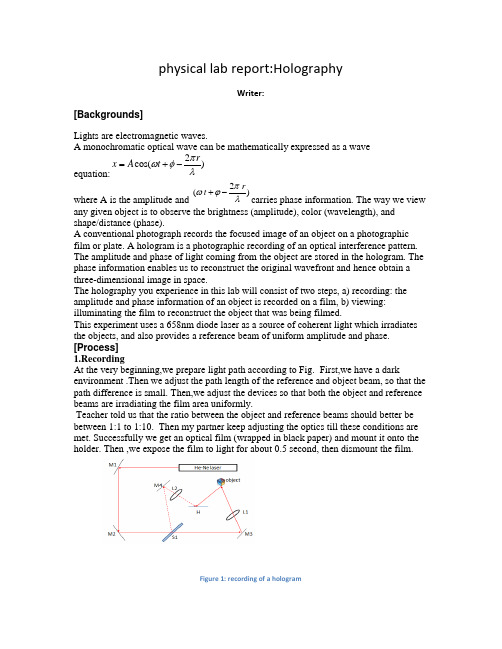
physical lab report:HolographyWriter:[Backgrounds]Lights are electromagnetic waves.A monochromatic optical wave can be mathematically expressed as a waveequation:2cos()r x A tπωφλ=+-where A is the amplitude and)2(λπϕωrt-+carries phase information. The way we viewany given object is to observe the brightness (amplitude), color (wavelength), and shape/distance (phase).A conventional photograph records the focused image of an object on a photographic film or plate. A hologram is a photographic recording of an optical interference pattern. The amplitude and phase of light coming from the object are stored in the hologram. The phase information enables us to reconstruct the original wavefront and hence obtain a three-dimensional image in space.The holography you experience in this lab will consist of two steps, a) recording: the amplitude and phase information of an object is recorded on a film, b) viewing: illuminating the film to reconstruct the object that was being filmed.This experiment uses a 658nm diode laser as a source of coherent light which irradiates the objects, and also provides a reference beam of uniform amplitude and phase. [Process]1.RecordingAt the very beginning,we prepare light path according to Fig. First,we have a dark environment .Then we adjust the path length of the reference and object beam, so that the path difference is small. Then,we adjust the devices so that both the object and reference beams are irradiating the film area uniformly.Teacher told us that the ratio between the object and reference beams should better be between 1:1 to 1:10. Then my partner keep adjusting the optics till these conditions are met. Successfully we get an optical film (wrapped in black paper) and mount it onto the holder. Then ,we expose the film to light for about 0.5 second, then dismount the film.Figure 1: recording of a hologram2.Film developmentAfter getting a film,we take it to the dark room to develop. There are three bath basins: developer, stop bath (water), and fixer. According to the instructor, we immerse the film into development liquid. My partner flip the film up and down with the tweezers and we wait till the gray-scale is similar to the color on the bottom of the basin. This usually takes 2 minutes and 25 seconds.Later,we rinse the film in the water basin for 25 seconds, and we take it to the fixer. I immerse it in the fixer for 3 minutes. We take the film to the viewing room and dry the film.3.ViewingThe principle to reconstruct image from a hologram is via light diffraction. If a laser beam irradiates onto the film exactly like the object beam, diffraction will happen on the pattern recorded on the hologram. See figure below.Figure 2: illustration of image reconstruction in hologram..We are all excited to get ready to view the film. Before viewing, we have a high expectation about it.We Use a viewing beam to irradiate the film. After having made sure the emulsion side is facing the beam, we adjust our viewing angle on the other side of the film to observe an expected 3-D image of the object.HOWEVER unfortunately,we are unlucky to find the image.No matter what angle we try,we can’t find it.We suppose it is because the angle is too large to find.So we try once again,LUCKLY,we finally find the 3-D image! -------A lovely white horse!![Feeling]In this experiment,we have a deep impression of the 3-D image. I think this experience is very unforgettable.In deed,this is where physics is attractive to us.。
简单的实验报告英语作文
简单的实验报告英语作文Experimental Report: The Effect of Temperature on the Rate of Enzyme Activity。
Introduction。
Enzymes are proteins that catalyze biochemicalreactions in living organisms. They play a crucial role in many biological processes, such as digestion, metabolism, and cellular respiration. Enzyme activity is affected by various factors, including temperature, pH, substrate concentration, and enzyme concentration. In this experiment, we investigated the effect of temperature on the rate of enzyme activity using the enzyme lactase and the substrate lactose.Materials and Methods。
Materials:Lactase solution。
Lactose solution。
Test tubes。
Thermometer。
Water bath。
Timer。
Spectrophotometer。
Methods:1. Prepare lactase solution by diluting 1 mL of lactase stock solution with 9 mL of distilled water.2. Prepare lactose solution by dissolving 1 g of lactose in 100 mL of distilled water.3. Label six test tubes as follows: 0°C, 20°C, 30°C, 40°C, 50°C, and 60°C.4. Add 2 mL of lactase solution to each test tube.5. Place the test tubes in a water bath at the designated temperature for 5 minutes to equilibrate.6. Add 2 mL of lactose solution to each test tube and start the timer.7. Mix the contents of each test tube by gently swirling.8. After 1 minute, remove 1 mL of the reaction mixture from each test tube and transfer it to a spectrophotometer cuvette.9. Measure the absorbance of each sample at 540 nm using a spectrophotometer.10. Repeat steps 8-9 every minute for 5 minutes.11. Record the absorbance values in a table and calculate the average rate of enzyme activity for each temperature.Results。
英语实验报告总结模板

Title: [Experiment Title]Date: [Date of Experiment]Objective:The primary objective of this experiment was to [state the main goal or research question of the experiment].Materials:- [List all the materials used in the experiment, including equipment, chemicals, samples, etc.]- [Specify any special or unique materials required]Procedure:1. [Step 1: Describe the first step of the experiment in detail.]2. [Step 2: Provide a detailed description of the second step.]3. [Continue listing steps in the same format, ensuring each step is clearly described.]4. [Final Step: Explain the last step of the experiment, including any data collection or observations.]Observations:- [Describe any visual, auditory, or tactile observations made during the experiment.]- [Record any unexpected occurrences or anomalies.]- [Include data collected during the experiment, such as measurements, times, or observations.]Results:- [Present the data collected during the experiment in a clear and organized manner. This could include tables, graphs, or charts.]- [Discuss the significance of the data in relation to the experiment's objective.]Analysis:- [Analyze the data collected and discuss how it supports or refutes the experiment's hypothesis or objective.]- [Discuss any trends or patterns observed in the data.]- [Explain any limitations of the experiment and how they might have affected the results.]Conclusion:- [Summarize the main findings of the experiment.]- [State whether the experiment's objective was achieved.]- [Discuss the implications of the results for the field of study or for further research.]Discussion:- [Compare the results of this experiment with those of similar experiments in the literature.]- [Discuss any theoretical or practical applications of the findings.]- [Suggest areas for future research based on the outcomes of this experiment.]References:- [List all the sources cited in the report, following the appropriate citation style.]Appendix:- [Include any additional information that may be relevant but not necessary for the main body of the report, such as raw data, detailed calculations, or additional graphs.]---Note: This template is a general guide and should be customizedaccording to the specific requirements of the experiment, the discipline, and the academic institution. The length of the report may vary based on the complexity of the experiment and the depth of the analysis required.。
英文实验报告范例
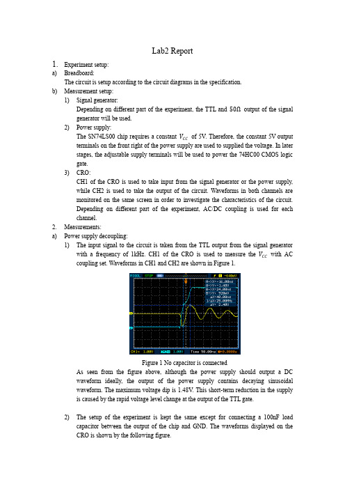
Lab2 Report1.Experiment setup:a)Breadboard:The circuit is setup according to the circuit diagrams in the specification.b)Measurement setup:1)Signal generator:Depending on different part of the experiment, the TTL and 50Ωoutput of the signalgenerator will be used.2)Power supply:The SN74LS00 chip requires a constant V CC of 5V. Therefore, the constant 5V outputterminals on the front right of the power supply are used to supplied the voltage. In laterstages, the adjustable supply terminals will be used to power the 74HC00 CMOS logicgate.3)CRO:CH1 of the CRO is used to take input from the signal generator or the power supply,while CH2 is used to take the output of the circuit. Waveforms in both channels aremonitored on the same screen in order to investigate the characteristics of the circuit.Depending on different part of the experiment, AC/DC coupling is used for eachchannel.2.Measurements:a)Power supply decoupling:1)The input signal to the circuit is taken from the TTL output from the signal generatorwith a frequency of 1kHz. CH1 of the CRO is used to measure the V CC with ACcoupling set. Waveforms in CH1 and CH2 are shown in Figure 1.Figure 1 No capacitor is connectedAs seen from the figure above, although the power supply should output a DCwaveform ideally, the output of the power supply contains decaying sinusoidalwaveform. The maximum voltage dip is 1.48V. This short-term reduction in the supplyis caused by the rapid voltage level change at the output of the TTL gate.2)The setup of the experiment is kept the same except for connecting a 100nF loadcapacitor between the output of the chip and GND. The waveforms displayed on theCRO is shown by the following figure.Figure 2 A load capacitor is connected at the outputThe load capacitor represents the total input impedances of all other logic gatesconnected to the output of this logic gate, which in turn gives a measure of the fan-out ofthe gate. After connecting the load capacitor, the voltage dip has increased to 2.10V.While the capacitor is charging up, it draws a lot current from the output of the chip.This causes the supply voltage to reduce to maintain the supply power constant.3)Connect a capacitor of 100nF across the V CC and GND while keeping the rest of thecircuit the same as the previous steps. After connecting the power supply decouplingcapacitor, the waveform of the power supply is recorded in the following figure.Figure 3 Decoupling capacitor is connectedIn comparison with the first case where there is no capacitor connected between V CCand GND, the decaying sinusoid is smoothened quiet a lot. The capacitor charges upwhen is supply voltage is stable and discharges to stablise the supply voltage level whenthe supply voltage undergoes a dip.b)Propagation delay:1)With load capacitor at the output:The low-to-high propagation delay is the change in time measured between the point halfway of the falling edge of the input signal and the point halfway of the corresponding rising edge of the output signal. The measurement is done using the cursor function of the CRO.Figure 4 Propagation delay with load capacitorThe low-to-high propagation delay specified in the data sheet for the 74LS00 chip is4.5ns under the condition of a load capacitor of 50pF. The capacitor we use is 100nFwhich is 2000 times of the value used in the data sheet. Then the expected value of t LHwould be 9μs. The measured value from the CRO is 10.4μs which is quite close to the expected value. The slight discrepancy maybe due to the capacitance present in the breadboard and wires. Since the measured value is very close to the expected value, it is still consistent with the datasheet.2)Without the load capacitor:Figure 5 Propagation delay without load capacitorAs the figure indicates that the propagation delay in this case is 16ns. When there is no load capacitor connected at the output of the chip, the transient time of the output waveform is reduced by a considerable amount. The propagation delay specified in the datasheet is in the range of 3 to 4.5ns under the test condition of R L=280ΩandC L=15pF. The discrepancy in the measured propagation delay could be due to thedifference in the test condition. However, the behavior of the output in this case is within expectation and thus consistent.c)Noise margins:The signal generator is set to produce a triangular waveform of 1kHz, with minimum voltage of 0V and maximum voltage at 5V. The output waveform is displayed on the CRO’s screen asshown in the Figure 7 and 8. Cursor function is used to measure the V IL,V IH,V OL and V OH. The V IH and V IL are measured to be 1.04V and 0.76V respectively, as shown in Figure 8 and 9. V OH and V OL are 4.40V and 80mV respectively (refer to Figure 10). The noise margin of a TTL gate is define to be: NM H=V OH−V IH and NM L=V IL−V OL. The noise margin of the 74LS00 gate is:NM H=4.40−1.04=3.36VNM L=0.76−0.08=0.68VThe values of V IL and V IH specified in the data sheet are 0.8V (max) and 2V (min). The measured V IL is consistent with the data sheet though it is a little bit high. The measured V IH, however is too low compared with the specified value. The discrepancy in the value of the measured V IH may be caused by that the datasheet is conservative on this value.The values of V OH and V OL specified in the data sheet are 2.7V (min), 3.4 (typical) and 0.5V (max) respectively. Those values measured from the experiment are within the range of specification and thus consistent with the data sheet.Figure 6 Output waveform Figure 7 Measure of V IHFigure 8 Measure of V ILVoltage transfer characteristics:The equipment settings and circuit are kept the same as the previous step except for CH2. The X-Y setting is used instead of T-Y in order to show how v OUT changes with v SIG. Figure 9 shows the final result of this part in the experiment. When the signal voltage is low, the output voltage is high and the converse. The graph shows that v OUT is decreasing as v SIG increases. Furthermore, there is a sudden drop in v OUT when v SIG is equal to the switching voltage. This is within our expectation. Therefore, the graph below is consistentwith the physical operation of the chip.Figure 9 V oltage transferd) Input and output characteristics:Part (a):Build up the circuit as shown in the following circuit diagram. The 1kΩ resistor is crucial in this case as it limits the current flow into the gate. The signal generator is set to produce a triangular wave of 1kHz with maximum voltage of 8V and minimum voltage of −4V . CH1 and CH2 are used to measure the voltage across the resistor at the output of the chip. The MATH function of the CRO is then used to calculate the potential difference across the resistor. The relation between i OUT and v IN is shown in the graph below.Figure 10 Figure11 V INR −V INFigure 12 Figure 13 V OUTR −V OUTPart (b)The circuit is setup according to Figure 12. The CRO, signal generator and power supply settings are kept unchanged. The experimental procedure is similar to that in part (a). The relationship between i OUT and v OUT is shown in the following graph. At either end of the graph, current is increasing dramatically with minimal increase/degrees of v OUT . This is dure to the diodes at the input and output sides of the chip. They are able to clamp the voltage at a stable level by draining a lot of current. Therefore the shape of the graph is consistent with the behavior of the chip.e) Low-voltage CMOS logic:Set up the circuit with the 74HC00 chip according to Figure 14 on the breadboard. The input signal to the circuit from the signal generator is a square wave at 1kHz with maximum and minimum voltages of 2 and 0volts. This can be achieved by adjusting the offset of the generator appropriately. Start the experiment with the supply voltage V CC =2V and gradually reduce it to find the point where the chip is not outputting a correct logic level.Figure 14 Figure 15 74HC00 correctly operatingWhen the supply voltage is at 2V, the output waveform is shown in Figure 15. As the blue trace (output logic measured by CH2) suggested that the chip is functioning correctly with a supply voltage of 2V.However, if we carefully reduce the supply voltage, until a distorted output logic is seen on the screen. The output waveform is shown in the Figure 16.Figure 16 74HC00 logic output distortedV CC is measured to be 0.9V at this instance. The output logic is not a square wave anymore.The data sheet for 74CH00 specifies that the operating voltage is between 2-6V. 0.9V is out of this range and the chip may not operate as we expected. Thus, the measured value is consistent with the data sheet.When V CC gets quiet low, the output waveform almost collapse into a flat line, except some fluctuations on it. When the supply voltage gets quiet low, the CMOS chip is not turned on and therefore the output logic state is incorrect. The fluctuations may be the noise in the components detected by the CRO.f)Interfacing CMOS and TTL:In Figure 23, a BJT is used to interface the CMOS and TTL gates. The circuit is basically a cascade of NAND gates to invert the input signal. At the first stage of the circuit, the CMOS gate inverts the input signal. Since the CMOS gate is operating at 1V supply voltage, outputlogic high will be 1V and 0V for logic low.The BJT is acting as an open collector which switches the output voltage between V CC and GND. When the output voltage of the CMOS gate is high (1V), current flows into the base of the transistor, the collector voltage will be pulled down to GND. This is because of the fact that the BJT is in its saturation mode. When the output voltage of the CMOS is low, no current flows into the base terminal, then the collector voltage will be pulled up to V CC=5V.The BJT is in its cut-off region in this case. Therefore the BJT pulls up the output logic high voltage level to V CC in order to better drive the TTL gate in the next stage of the circuit.The circuit is setup on the breadboard according to the circuit diagram in Figure 20. The supply voltage to the COMS gate is 1V while 5V for BJT and TTL. The output voltage at each stage of the circuit is measured by CH2 of the CRO. By investigating the output waveforms in Figure 17 to 19, it is concluded that the explanation of the operation of the circuit is consistent with the actual experimental result.Figure 17 Output of CMOS Figure 18 Output of BJTFigure 19 Output of TTL Figure 20 Interfacing CMOS and TTL 3.Conclusion:In this experiment, we have investigated the fan-out, propagation delay, noise margins and I/O characteristics of a TTL gate. Apart from a few discrepancies, the result is consistent with the specified values in the datasheet. A CMOS logic gate is investigated for its low-voltage performance and CMOS-TTL interface. The experiment result demonstrates that the CMOS gate has a much better power rating as compared to TTL gates. A pull-up circuit such as the open collector switch is required to interface the two. This experiment successfully demonstrates the important features and behaviors of TTL, CMOS gates and their interface.。
- 1、下载文档前请自行甄别文档内容的完整性,平台不提供额外的编辑、内容补充、找答案等附加服务。
- 2、"仅部分预览"的文档,不可在线预览部分如存在完整性等问题,可反馈申请退款(可完整预览的文档不适用该条件!)。
- 3、如文档侵犯您的权益,请联系客服反馈,我们会尽快为您处理(人工客服工作时间:9:00-18:30)。
大学物理实验报告Ferroelectric Control of Spin PolarizationControlling the spin degree of freedom by purely electrical means is currently an important challenge in spintronics (1, 2). Approaches based on spin-transfer torque (3) have proven very successful in controlling the direction of magnetization in a ferromagnetic layer, but they require the injection of high current densities. An ideal solution would rely on the application of an electric field across an insulator, as in existing nanoelectronics. Early experiments have demonstrated the volatile modulation of spin-based properties with a gate voltage applied through a dielectric. Notable examples include the gate control of the spin-orbit interaction in III-V quantum wells (4), the Curie temperature T C(5), or the magnetic anisotropy (6) in magnetic semiconductors with carrier-mediated exchange interactions; for example, (Ga,Mn)As or (In,Mn)As. Electric field–induced modifications of magnetic anisotropy at room temperature have also been reported recently in ultrathin Fe-based layers (7, 8).A nonvolatile extension of this approach involves replacing the gate dielectric by a ferroelectric and taking advantage of the hysteretic response of its order parameter (polarization) with an electric field. When combined with (Ga,Mn)As channels, for instance, a remanent control of T C over a few kelvin was achieved throughpolarization-driven charge depletion/accumulation (9, 10), and the magnetic anisotropy was modified by the coupling of piezoelectricity and magnetostriction (11, 12). Indications of an electrical control of magnetization have also been provided in magnetoelectric heterostructures at room temperature (13–17).Recently, several theoretical studies have predicted that large variations of magnetic properties may occur at interfaces between ferroelectrics and high-T C ferromagnets such as Fe (18–20), Co2MnSi (21), or Fe3O4(22). Changing the direction of the ferroelectric polarization has been predicted to influence not only the interfacial anisotropy and magnetization, but also the spin polarization. Spin polarization [., the normalized difference in the density of states (DOS) of majority and minority spin carriers at the Fermi level (E F)] is typically the key parameter controlling the response of spintronics systems, epitomized by magnetic tunnel junctions in which the tunnel magnetoresistance (TMR) is related to the electrode spin polarization by the Jullière formula (23). These predictions suggest that the nonvolatile character of ferroelectrics at the heart of ferroelectric random access memory technology (24) may be exploited in spintronics devices such as magnetic random access memories or spin field-effect transistors (2). However, the nonvolatile electrical control of spin polarization has not yet been demonstrated.We address this issue experimentally by probing the spin polarization of electrons tunneling from an Fe electrode through ultrathin ferroelectric BaTiO3(BTO) tunnel barriers (Fig. 1A). The BTO polarization can be electrically switched to point toward or away from the Fe electrode. We used a half-metallic (25) bottom electrode as a spin detector in these artificial multiferroic tunnel junctions (26, 27). Magnetotransport experiments provide evidence for a large and reversible dependence of the TMR on ferroelectric polarization direction.Fig. 1(A) Sketch of the nanojunction defined by electrically controlled nanoindentation. A thin resist is spin-coated on the BTO(1 nm)/LSMO(30 nm) bilayer. The nanoindentation is performed with a conductive-tip atomic force microscope, and the resulting nano-hole is filled by sputter-depositing Au/CoO/Co/Fe. (B) (Top) PFM phase image of a BTO(1 nm)/LSMO(30 nm) bilayer after poling the BTO along 1-by-4–μm stripes with either a negative or positive (tip-LSMO) voltage. (Bottom) CTAFM image of an unpoled area of a BTO(1 nm)/LSMO(30 nm) bilayer. Ω, ohms. (C) X-ray absorption spectra collected at room temperature close to the Fe L3,2(top), Ba M5,4(middle), and Ti L3,2(bottom) edges on an AlO x nm)/Al nm)/Fe(2 nm)/BTO(1 nm)/LSMO(30 nm)(D) HRTEM and (E) HAADF images of the Fe/BTO interface in a Ta(5 nm)/Fe(18 nm)/BTO(50 nm)/LSMO(30 nm)The white arrowheads in (D) indicate the lattice fringes of {011} planes in the iron layer. [110] and [001] indicate pseudotetragonal crystallographic axes of the BTO perovskite.The tunnel junctions that we used in this study are based on BTO(1 nm)/LSMO(30 nm) bilayers grown epitaxially onto (001)-oriented NdGaO3(NGO) single-crystal substrates (28). The large (~180°) and stable piezoresponse force microscopy (PFM) phase contrast (28) between negatively and positively poled areas (Fig. 1B, top) indicates that the ultrathin BTO films are ferroelectric at room temperature (29). The persistence of ferroelectricity for such ultrathin films of BTO arises from the large lattice mismatch with the NGO substrate (–%), which is expected to dramatically enhance ferroelectric properties in this highly strained BTO (30). The local topographical and transport properties of the BTO(1 nm)/LSMO(30 nm) bilayers were characterized by conductive-tipatomic force microscopy (CTAFM) (28). The surface is very smooth with terraces separated by one-unit-cell–high steps, visible in both the topography (29) and resistance mappings (Fig. 1B, bottom). No anomalies in the CTAFM data were observed over lateral distances on the micrometer scale.We defined tunnel junctions from these bilayers by a lithographic technique based on CTAFM (28, 31). Top electrical contacts of diameter ~10 to 30 nm can be patterned by this nanofabrication process. The subsequent sputter deposition of a 5-nm-thick Fe layer, capped by a Au(100 nm)/CoO nm)/Co nm) stack to increase coercivity, defined a set of nanojunctions (Fig. 1A). The same Au/CoO/Co/Fe stack was deposited on another BTO(1 nm)/LSMO(30 nm) sample for magnetic measurements. Additionally, a Ta(5 nm)/Fe(18 nm)/BTO(50 nm)/LSMO(30 nm) sample and a AlO x nm)/Al nm)/Fe(2 nm)/BTO(1 nm)/LSMO(30 nm) sample were realized for structural and spectroscopic characterizations.We used both a conventional high-resolution transmission electron microscope (HRTEM) and the NION UltraSTEM 100 scanning transmission electron microscope (STEM) to investigate the Fe/BTO interface properties of the Ta/Fe/BTO/LSMO sample. The epitaxial growth of the BTO/LSMO bilayer on the NGO substrate was confirmed by HRTEM andhigh-resolution STEM images. The low-resolution, high-angle annular dark field (HAADF) image of the entire heterostructure shows the sharpness of the LSMO/BTO interface over the studied area (Fig. 1E, top). Figure 1D reveals a smooth interface between the BTO and the Fe layers. Whereas the BTO film is epitaxially grown on top of LSMO, the Fe layer consists of textured nanocrystallites. From the in-plane (a) and out-of-plane (c) lattice parameters in the tetragonal BTO layer, we infer that c/a= ± , in good agreement with the value of found with the use of x-ray diffraction (29). The interplanar distances for selected crystallites in the Fe layer [., ~ Å(Fig. 1D, white arrowheads)] are consistent with the {011} planes of body-centered cubic (bcc) Fe. We investigated the BTO/Fe interface region more closely in the HAADF mode of the STEM (Fig. 1E, bottom). On the BTO side, the atomically resolved HAADF image allows thedistinction of atomic columns where the perovskite A-site atoms (Ba) appear as brighter spots. Lattice fringes with the characteristic {100} interplanar distances of bcc Fe (~ Å) can be distinguished on the opposite side. Subtle structural, chemical, and/or electronic modifications may be expected to occur at the interfacial boundary between the BTO perovskite-type structure and the Fe layer. These effects may lead to interdiffusion of Fe, Ba, and O atoms over less than 1 nm, or the local modification of the Fe DOS close to E F, consistent with ab initio calculations of the BTO/Fe interface (18–20).To characterize the oxidation state of Fe, we performed x-ray absorption spectroscopy (XAS) measurements on a AlO x nm)/Al nm)/Fe(2 nm)/BTO(1 nm)/LSMO(30 nm) sample (28). The probe depth was at least 7 nm, as indicated by the finite XAS intensity at the La M4,5edge (28), so that the entire Fe thickness contributed substantially to the signal. As shown in Fig. 1C(top), the spectrum at the Fe L2,3edge corresponds to that of metallic Fe (32). The XAS spectrum obtained at the Ba M4,5edge (Fig. 1C, middle) is similar to that reported for Ba2+in (33). Despite the poor signal-to-noise ratio, the Ti L2,3edge spectrum (Fig. C, bottom) shows the typical signature expected for a valence close to 4+ (34). From the XAS, HRTEM, and STEM analyses, we conclude that the Fe/BTO interface is smooth with no detectable oxidation of the Fe layer within a limit of less than 1 nm.After cooling in a magnetic field of 5 kOe aligned along the [110] easy axis of pseudocubic LSMO (which is parallel to the orthorhombic [100] axis of NGO), we characterized the transport properties of the junctions at low temperature K). Figure 2A(middle) shows a typical resistance–versus–magnetic field R(H) cycle recorded at a bias voltage of –2 mV (positive bias corresponds to electrons tunneling from Fe to LSMO). The bottom panel of Fig. 2A shows the magnetic hysteresis loop m(H) of a similar unpatterned sample measured with superconducting quantum interference device (SQUID) magnetometry. When we decreased the magnetic field from a large positive value, theresistance dropped in the –50 to –250 Oe range and then followed a plateau down to –800 Oe, after which it sharply returned to the high-resistance state. We observed a similar response when cycling the field back to large positive values. A comparison with the m(H) loop indicates that the switching fields in R(H) correspond to changes in the relative magnetic configuration of the LSMO and Fe electrodes from parallel (at high field) to antiparallel (at low field). The magnetically softer LSMO layer switched at lower fields (50 to 250 Oe) compared with the Fe layer, for which coupling to the exchange-biased Co/CoO induces larger and asymmetric coercive fields (–800 Oe, 300 Oe). The observed R(H) corresponds to a negative TMR= (R ap–R p)/R ap of –17%[R p and R ap are the resistance in the parallel (p) and antiparallel (ap) magnetic configurations, respectively; see the sketches in Fig. 2A]. Within the simple Jullière model of TMR(23) and considering the large positive spin polarization ofhalf-metallic LSMO (25), this negative TMR corresponds to a negative spin polarization for bcc Fe at the interface with BTO, in agreement with ab initio calculations (18–20).Fig. 2(A) (Top) Device schematic with black arrows to indicate magnetizations. p, parallel; ap, antiparallel. (Middle) R(H) recorded at –2 mV and K showing negative TMR. (Bottom) m(H) recorded at 30 K with a SQUID magnetometer. emu, electromagnetic units.(B) (Top) Device schematic with arrows to indicate ferroelectric polarization.(Bottom) I(V DC) curves recorded at K after poling the ferroelectric down (orange curve) or up (brown curve). The bias dependence of the TER is shown in the inset.As predicted (35–38) and demonstrated (29) previously, the tunnel current across a ferroelectric barrier depends on the direction of the ferroelectric polarization. We also observed this effect in our Fe/BTO/LSMO junctions. As can be seen in Fig. 2B, after poling the BTO at K to orient its polarization toward LSMO or Fe (with a poling voltage of VP–≈ –1 V or VP+≈ 1 V, respectively; see Fig. 2B sketches),current-versus-voltage I(V DC) curves collected at low bias voltages showed a finite difference corresponding to a tunnel electroresistance as large as TER=(I VP+–I VP–)/I VP–≈ 37% (Fig. 2B, inset). This TER can be interpreted within an electrostatic model (36–39), taking into account the asymmetric deformation of the barrier potential profile that is created by the incomplete screening of polarization charges by different Thomas-Fermi screening lengths at Fe/BTO and LSMO/BTO interfaces. Piezoelectric-related TER effects (35, 38) can be neglected as the piezoelectric coefficient estimated from PFM experiments is too small in our clamped films(29). TER measurements performed on a BTO(1 nm)/LSMO(30 nm) bilayer with the use ofa CTAFM boron-doped diamond tip as the top electrode showed values of ~200% (29). Given the strong sensitivity of the TER on barrier parameters and barrier-electrode interfaces, these two values are not expected to match precisely. We anticipate that the TER variation between Fe/BTO/LSMO junctions and CTAFM-based measurements is primarily the result of different electrostatic boundary conditions.Switching the ferroelectric polarization of a tunnel barrier with voltage pulses is also expected to affect the spin-dependent DOS of electrodes at a ferromagnet/ferroelectric interface. Interfacial modifications of the spin-dependent DOS of the half-metallic LSMO by the ferroelectric BTO are not likely, as no states are present for the minority spins up to ~350 meV above E F(40, 41). For 3d ferromagnets such as Fe, large modificationsof the spin-dependent DOS are expected, as charge transfer between spin-polarized empty and filled states is possible. For the Fe/BTO interface, large changes have been predicted through ab initio calculations of 3d electronic states of bcc Fe at the interface with BTO by several groups (18–20).To experimentally probe possible changes in the spin polarization of the Fe/BTO interface, we measured R(H) at a fixed bias voltage of –50 mV after aligning the ferroelectric polarization of BTO toward Fe or LSMO. R(H) cycles were collected for each direction of the ferroelectric polarization for two typical tunnel junctions of the same sample (Fig. 3, B and C, for junction #1; Fig. 3, D and E, for junction #2). In both junctions at the saturating magnetic field, high- and low-resistance states are observed when the ferroelectric polarization points toward LSMO or Fe, respectively, with a variation of ~ 25%. This result confirms the TER observations in Fig. 2B.Fig. 3(A) Sketch of the electrical control of spin polarization at the Fe/BTO interface.(B and C) R(H) curves for junction #1 (V DC= –50 mV, T= K) after poling the ferroelectric barrier down or up, respectively. (D and E) R(H) curves for junction #2 (V DC= –50 mV, T= K) after poling the ferroelectric barrier down or up, respectively. More interestingly, here, the TMR is dramatically modified by the reversal of BTO polarization. For junction #1, the TMR amplitude changes from –17 to –3% when the ferroelectric polarization is aligned toward Fe or LSMO, respectively (Fig. 3, B and C). Similarly for junction #2, the TMR changes from –45 to –19%. Similar resultswere obtained on Fe/BTO nm)/LSMO junctions (28). Within the Jullière model (23), these changes in TMR correspond to a large (or small) spin polarization at the Fe/BTO interface when the ferroelectric polarization of BTO points toward (or away from) the Fe electrode. These experimental data support our interpretation regarding the electrical manipulation of the spin polarization of the Fe/BTO interface by switching the ferroelectric polarization of the tunnel barrier.To quantify the sensitivity of the TMR with the ferroelectric polarization, we define a term, the tunnel electromagnetoresistance, as TEMR= (TMR VP+–TMR VP–)/TMR VP–. Large values for the TEMR are found for junctions #1 (450%) and #2 (140%), respectively. This electrical control of the TMR with the ferroelectric polarization is repeatable, as shown in Fig. 4for junction #1 where TMR curves are recorded after poling the ferroelectric up, down, up, and down, sequentially (28).Fig. 4TMR(H) curves recorded for junction #1 (V DC= –50 mV, T= K) after poling the ferroelectric up (VP+), down (VP–), up (VP+), and down (VP–).For tunnel junctions with a ferroelectric barrier and dissimilar ferromagnetic electrodes, we have reported the influence of the electrically controlled ferroelectric barrier polarization on the tunnel-current spin polarization. This electrical influence over magnetic degrees of freedom represents a new and interfacial magnetoelectric effect that is large because spin-dependent tunneling is very sensitive to interfacial details. Ferroelectrics can provide a local, reversible, nonvolatile, and potentially low-power means of electrically addressing spintronics devices.Supporting Online Materialand MethodsFigs. S1 to S5ReferencesReceived for publication 30 October 2009.Accepted for publication 4 January 2010.References and Notes1. C. Chappert, A. Fert, F. N. Van Dau, The emergence of spinelectronics in data storage. Nat. Mater. 6,813 (2007).2.I. Žutić, J. Fabian, S. Das Sarma, Spintronics: Fundamentalsand applications. Rev. Mod. Phys. 76,323 (2004).3.J. C. Slonczewski, Current-driven excitation of magneticmultilayers. J. Magn. Magn. Mater. 159, L1(1996).4.J. Nitta, T. Akazaki, H. Takayanagi, T. Enoki, Gate control of spin-orbit interaction in an inverted heterostructure. Phys.Rev. Lett. 78, 1335 (1997).5.H. Ohno et al., Electric-field control offerromagnetism. Nature 408, 944 (2000).6. D. Chiba et al., Magnetization vector manipulation by electricfields. Nature 455, 515 (2008).7.M. Weisheit et al., Electric field–induced modification of magnetismin thin-film ferromagnets. Science315, 349 (2007).8.T. Maruyama et al., Large voltage-induced magnetic anisotropy changein a few atomic layers of . Nanotechnol. 4, 158 2009).9.S. W. E. Riester et al., Toward a low-voltage multiferroic transistor:Magnetic (Ga,Mn)As under ferroelectric control. Appl. Phys.Lett. 94, 063504 (2009).10.I. Stolichnov et al., Non-volatile ferroelectric control offerromagnetism in (Ga,Mn)As. Nat. Mater. 7, 464(2008).11. C. Bihler et al., Ga1−x Mn x As/piezoelectric actuator hybrids: A modelsystem for magnetoelastic magnetization manipulation. Phys. Rev.B 78, 045203 (2008).12.M. Overby, A. Chernyshov, L. P. Rokhinson, X. Liu, J.K. Furdyna, GaMnAs-based hybrid multiferroic memory device. Appl. Phys.Lett. 92, 192501 (2008).13. C. Thiele, K. Dörr, O. Bilani, J. Rödel, L. Schultz, Influence of strain on the magnetization and magnetoelectric effectin 75, 054408 (2007).14.W. Eerenstein, M. Wiora, J. L. Prieto, J. F. Scott, N.D. Mathur, Giant sharp and persistent converse magnetoelectric effects inmultiferroic epitaxial heterostructures. Nat. Mater. 6, 348 (2007).15.T. Kanki, H. Tanaka, T. Kawai, Electric control of roomtemperature ferromagnetism in a Pb field-effect transistor. Appl. Phys.Lett. 89, 242506 (2006).16.. Chu et al., Electric-field control of local ferromagnetism using amagnetoelectric multiferroic. Nat. Mater. 7, 478 2008).17.S. Sahoo et al., Ferroelectric control of magnetism in BaTiO3∕Feheterostructures via interface strain coupling. Phys. Rev.B 76, 092108 (2007).18.. Duan, S. S. Jaswal, E. Y. Tsymbal, Predicted magnetoelectriceffect in Fe/BaTiO3multilayers: Ferroelectric control of magnetism. Phys. Rev.Lett. 97, 047201 (2006).19.M. Fechner et al., Magnetic phase transition in two-phasemultiferroics predicted from first . Rev. B 78, 212406 (2008).20.J. Lee, N. Sai, T. Cai, Q. Niu, A. A. Demkov, preprint available at abs/.21.K. Yamauchi, B. Sanyal, S. Picozzi, Interface effects at ahalf-metal/ferroelectric junction. Appl. Phys. Lett. 91, 062506 (2007). 22.M. K. Niranjan, J. P. Velev, . Duan, S. S. Jaswal, E.Y. Tsymbal, Magnetoelectric effect at the Fe3O4/BaTiO3(001) interface: A first-principles study. Phys. Rev. B 78, 104405 (2008).23.M. Jullière,Tunneling between ferromagnetic films. Phys. Lett.A 54, 225 (1975).24.J. F. Scott, Applications of modern ferroelectrics. Science 315, 954 (2007).25.M. Bowen et al., Nearly total spin polarization in La2/3Sr1/3MnO3fromtunneling experiments. Appl. Phys. Lett. 82, 233 (2003).26.J. P. Velev et al., Magnetic tunnel junctions with ferroelectricbarriers: Prediction of four resistance states from first principles. Nano Lett. 9, 427 (2009).27. F. Yang et al., Eight logic states of tunnelingmagnetoelectroresistance in multiferroic tunnel . Appl.Phys. 102, 044504 (2007).28.Materials and methods are available as supporting materialon Science Online.29.V. Garcia et al., Giant tunnel electroresistance for non-destructivereadout of ferroelectric states. Nature460, 81 (2009).30.K. J. Choi et al., Enhancement of ferroelectricity in strainedBaTiO3thin films. Science 306, 1005(2004).31.K. Bouzehouane et al., Nanolithography based on real-timeelectrically controlled indentation with an atomic force microscope fornanocontact elaboration. Nano Lett. 3, 1599 (2003).32.T. J. Regan et al., Chemical effects at metal/oxide interfaces studiedby x-ray-absorption . Rev. B 64, 214422 (2001).33.N. Hollmann et al., Electronic and magnetic properties of the kagomesystems YBaCo4O7and YBaCo3M O7(M=Al, Fe). Phys. Rev. B 80, 085111 (2009).34.M. Abbate et al., Soft-x-ray-absorption studies of the location ofextra charges induced by substitution in controlled-valence materials. Phys. Rev.B 44, 5419 (1991).35. E. Y. Tsymbal, H. Kohlstedt, Tunneling across aferroelectric. Science 313, 181 (2006).36.M. Ye. Zhuravlev, R. F. Sabirianov, S. S. Jaswal, E.Y. Tsymbal, Giant electroresistance in ferroelectric tunnel junctions. Phys.Rev. Lett. 94, 246802 (2005).37.M. Ye. Zhuravlev, R. F. Sabirianov, S. S. Jaswal, E.Y. Tsymbal, Erratum: Giant electroresistance in ferroelectric tunneljunctions. Phys. Rev. Lett. 102, 169901 2009).38.H. Kohlstedt, N. A. Pertsev, J. RodriguezContreras, R. Waser, Theoretical current-voltage characteristics offerroelectric tunnel junctions. Phys. Rev. B 72, 125341 (2005).39.M. Gajek et al., Tunnel junctions with multiferroic barriers. Nat.Mater. 6, 296 (2007).40.M. Bowen et al., Spin-polarized tunneling spectroscopy in tunneljunctions with half-metallic . Rev. Lett. 95, 137203 (2005).41.J. D. Burton, E. Y. Tsymbal, Prediction of electrically inducedmagnetic reconstruction at the manganite/ferroelectric interface. Phys. Rev.B 80, 174406 (2009).42.We thank R. Guillemet, C. Israel, M. E. Vickers, R. Mattana, . George,and P. Seneor for technical assistance, and C. Colliex for fruitful discussions on the microscopy measurements. This study was partially supported by the .Partenariat Hubert Curien Alliance program, the French Réseau Thématique de Recherche Avancée Triangle de la Physique, the European Union (EU) Specific Targeted Research Project (STRep) Manipulating the Coupling in Multiferroic Films, EU STReP Controlling Mesoscopic Phase Separation, . Engineering and Physical Sciences Research Council grant EP/E026206/I, French C-Nano Île de France, French Agence Nationale de la Recherche (ANR) Oxitronics, French ANR Alicante, the European Enabling Science and Technology through European Elelctron Microscopy program, and the French Microscopie Electronique et Sonde Atomique network. .acknowledges support from Comissionat per a Universitats i Recerca (Generalitat de Catalunya).。