AOT LED 3014规格书
LED3014规格书

Reel Dimensions
Note:.Tolerance unless mentioned is ±0.1mm; Unit = mm
Carrier Tape Dimensions: Loaded Quantity 4000 pcs Per Reel
Note:.Tolerance unless mentioned is ±0.1mm; Unit = mm
Note: The products are sensitive to static electricity and must be carefully taken when handling products.
Electro-Optical Characteristics(Ta=25℃)
Parameter
Bin Code V1 V2 V3 V4 V5 V6 V7 V8
Min. 2.8 2.9 3.0 3.1 3.2 3.3 3.4 3.5
Max. 2.9 3.0 3.1 3.2 3.3 3.4 3.5 3.6
Tolerance of Forward Voltage: ±0.1V
Bin Range of Luminous Intensity
Top view white LEDs. White SMT package. Lead frame package with individual 2 pins. Wide viweing angle. Soldering methods: IR reflow soldering. Pb-free. The product itself will remain within RoHS compliant version.
3014贴片(正白)规格书

深圳巨佳鑫光电科技有限公司承 认 书SPECIFICATION FOR APPROVAL客户Customer类别TypeSMD 贴片 规格DESCRIPTION3014正白光 型号Part NoJJX-3014WEDT-U0130客户单号Order No样品档案号REF.NO送样日期Date数量Amount承认书份数Copy of Document1份请确认样品,并回复我司有关您的建议,谢谢!Please confirmatory sample,and give us for your valuable suggestion.Thanks!地址: 深圳市龙岗区爱联爱南路495号FACTORY: 495,Ailian ainan road ,Longgang District Shenzhen City,Guangdong Province,ChinaTEL:86-0755-******** Fax: 86-0755-******** E-mail:cqs926@ 客 户 承 认 回 签Approved By Customer核 准Qualified By制 作Form Designer陈文胜 张俊JJX-3014WEDT-U0130SMD LED深圳巨佳鑫光电科技有限公司※Features1.Outline Package:3.0*1.4*0.8MM( TOP View White LED)2.Lens Appearance:Yellow Disffusepliant with RoHS※ Product codeJ J X O p to -e le c tro n in c sa c k s g e c o d eR e e lp a c k a g in gm ittin g c o lo r T h e c ir c u itry c o d e D iffu s e d P a c k a g e d im e n s io n m ittin g c o lo r T h e c ir c u itrv c o d e P c -w h ite u m b e r o f c h ip s c o d eic e c o d e o r th e L u m in o u s In te n s ity T h e E le c tric s※ Package Outlines (±0.1mm)JJX-3014WEDT-U0130SMD LED深圳巨佳鑫光电科技有限公司※Maximum RatingsParameterSymbolValuesUnitOperating temperature range T op – 40 … + 100 °C Storage temperature range T stg – 40 … + 100 °CJunction temperature T j 120 °C Forward current (TA=25°C) I F 40 mA Surge currentt ≤ 10 μs, D = 0.005, TA=25°C I F 200 mA Reverse voltage(I R = 10uA,TA=25°C) V R 5 V Power consumption (TA=25°C) P tot 70 mW Thermal resistance solder pointR th-js 45 °C /W Electrostatic Discharge ESD 2000(HBM)VViewing angle at 50 % ΦV 2ϕ120 deg.Reverse current (V R =5V)I R 10 uA※Characteristics (T A = 25 °C)lten Symbol condition Min Typ Max UnitV30 2.8 2.9 3.0V32 3.0 3.12 3.2V34 3.2 3.27 3.4 Forward V oltageV36VF IF=30MA 3.4 3.5 3.6VL13 300032003300 Luminous lntensity L14 IV IF=30MA 33013480 3600MCDNOTE:1.Tolerance of luminous intensity is ±10% 2.Tolerance of torward voltage is ±0.05VJJX-3014WEDT-U0130SMD LED深圳巨佳鑫光电科技有限公司Relative Spectral EmissionV(λ) = Standard eye response curve Φrel = f (λ); T A = 25 °C; I F= 30mARadiation CharacteristicΦrel = f (ϕ); T A = 25 °C0%10%20%30%40%50%60%70%80%90%100%-100-80-60-40-20020406080100AngleL u m i n o u s i n t e n s i t y r e l a t i v e v a l u eJJX-3014WEDT-U0130SMD LED深圳巨佳鑫光电科技有限公司Forward CurrentI F = f (V F ); T A = 25 °C2.02.22.42.62.83.03.23.43.63.84.04.24.4VF(V)Relative Luminous IntensityI V /I V (30mA) = f (I F ); T A= 25 °C0.20.40.60.811.21.41.61.822.22.42.62.833.23.40102030405060708090100110IF(mA)I V /I V (@I F =20m A )Chromaticity Coordinate Shift x, y = f (I F ); T A= 25 °C 0.270.280.290.30.310.320.33020406080100120IF(mA)C I E x ,y Max. Permissible Forward Current I F = f (T)JJX-3014WEDT-U0130SMD LED深圳巨佳鑫光电科技有限公司※Reliability(1)TEST ITEMS AND RESULTSTypeTest Item Ref.StandardTest ConditionsNoteNumber of DamagedResistance to Soldering Heat(Reflow Soldering)JESD22-B106Tsld=260ºC,10sec 2times 0/22Twmperature CycleJESD22-A10440ºC 30min ↑↓5min 100ºC 30min 1000 cycle0/100Thermal Shock JESD22-A10640ºC 15min ↑↓ 100ºC 15min 1000 cycle 0/100High TemperatureStorage JESD22-A103Ta=100ºC 1000 hrs 0/100 Low TemperatureStorage JESD22-A119Ta=40ºC 1000 hrs0/100E n v i r o n m e n t a l S e q u e n c ePower temperaturecyclingJESD22-A105On 5min -40ºC>15min ↑↓ ↑↓<15min Off5min 100ºC>15min100 cycle 0/100Life Test JESD22-A108Ta=100ºCI F =30mA1000 hrs0/100 O p e r a t i o n S e q u e n c eHigh Humidity HeatLife TestJESD22-A10160ºC RH=90%I F =20mA1000 hrs0/100(2)CRITERIA FOR JUDGING THE DAMAGECriteria for JudgementItemSymbolTest ConditionsMinMax Fonward Voltage VF IF=10mA — U.S.L﹡)×1.1 Reverse C 坐 IR VR=5V —U.S.L﹡)×2.0Luminous IntensityIVIF=10mAU.S.L﹡﹡)×0.7—U.S.L.:Upper Standard Level L.S.L.:Lower Standard LevelJJX-3014WEDT-U0130SMD LED深圳巨佳鑫光电科技有限公司※ Packaging SpecificationsNOTES1.Empty component pockets are sealed with top cover tape:2.The maximum number of missing lamps two :3.The cathode is oriented towards the tape sprocket hole:4.4000pcs/reel.JJX-3014WEDT-U0130SMD LED深圳巨佳鑫光电科技有限公司※Packaging Specifications in box※Label DdscriptionJJX-3014WEDT-U0130SMD LED深圳巨佳鑫光电科技有限公司※CIE Specifications※Chromaticity Coordinate Groups (I F =30mA) Group X1 Y1 X2 Y2 X3Y3X4Y4CZ3 0.3014 0.3294 0.30880.3403 0.3113 0.3338 0.3041 0.3238CZ4 0.3041 0.3238 0.31130.3338 0.3139 0.3278 0.3069 0.3182CZ5 0.3069 0.3182 0.31390.3278 0.316 0.3218 0.3095 0.3126CZ6 0.3095 0.3126 0.316 0.3218 0.3183 0.3162 0.3121 0.3072WA3 0.3088 0.3403 0.31640.3497 0.3183 0.3427 0.3113 0.3338WA4 0.3113 0.3338 0.31830.3427 0.3201 0.336 0.3139 0.3278WA5 0.3139 0.3278 0.32010.336 0.3219 0.3296 0.316 0.3218WA6 0.316 0.3218 0.32190.3296 0.3239 0.3228 0.3183 0.3162WB3 0.3164 0.3497 0.32340.3592 0.3249 0.3519 0.3183 0.3427WB4 0.3183 0.3427 0.325 0.3519 0.3265 0.3448 0.3201 0.336 WB5 0.3201 0.336 0.32650.3448 0.3281 0.3379 0.3219 0.3296WB6 0.3219 0.3296 0.32810.3379 0.3297 0.3309 0.3239 0.3228WC3 0.3234 0.3592 0.33250.3717 0.3335 0.3637 0.3249 0.3519WC4 0.3249 0.3519 0.33350.3637 0.3344 0.3563 0.3265 0.3448WC5 0.3265 0.3448 0.33440.3563 0.3354 0.3479 0.3281 0.3379WC6 0.3281 0.3379 0.33540.3479 0.3365 0.3397 0.3297 0.3309WD3 0.3325 0.3717 0.34060.3838 0.3413 0.3752 0.3335 0.3637WD4 0.3335 0.3637 0.34130.3752 0.3419 0.3664 0.3344 0.3563WD5 0.3344 0.3563 0.34190.3664 0.3426 0.3576 0.3354 0.3479WD60.3354 0.3479 0.34260.3576 0.3434 0.3487 0.3365 0.3397JJX-3014WEDT-U0130SMD LED深圳巨佳鑫光电科技有限公司※Ordering InformationNote: No packing unit/tape ever contains more than one group for each selection.※Recommended Solder PadIR Reflow SolderingSoldering Conditions Preconditioning acc. to JEDEC Level 2IR Reflow Soldering Profile for lead free soldering (acc. to J-STD-020B)Cautions1. Recommended storage condition: At 20℃~30℃ and relative humidity 70% RH max.2. After this bag is opened, devices that will be applied to infrared reflow, vapor-phase reflow,or equivalent soldering process must be: a. Completed within 24hours. b. Stored at less than 30% RH.3. Devices require baking before mounting, if: 2a or 2b is not met.4. If baking is required, devices must be baked under blow conditions: 12hours at 75℃±3℃Luminous Intensity (I F = 30mA) TypeColor of EmissionMin I V (mcd)MAX I V (mcd)JJX-3014WEDT-U0130 White30003600。
3014灯珠规格书

测试周期 100 循环 1000 小时 1000 小时 1000 小时 1000 小时 1000 小时 1000 小时 3次 3次
不良数量 0/50 0/50 0/50 0/50 0/50 0/50 0/50 0/50 0/50
8
7.规格尺寸
Dated : 03/01/2013 Rev: 01
Dated : 03/01/2013 Rev: 01
3014 灯珠规格书
ZT3014WOS1
1
目录
1.灯珠描述 2.最大额定值 3.光电参数 4.典型光电特性曲线 5.分光标准 6.可靠性测试 7.规格尺寸 8.料盘结构和包装 9.回流焊 10.使用注要事项
Dated : 03/01/2013 Rev: 01
注释: 1.所有尺寸单位为毫米 2.如果无其它注明,公差范围通常采用±0.1 毫米。 8.料盘结构和包装
建议焊盘尺寸
包装标签
数量
流明值
BIN 区 正向电压
9
项目 盘 盒 箱
9. 回流焊
Dated : 03/01/2013 Rev: 01
包装规格和数量 数量
4,000pcs 7 reels 5 boxes
183℃
无铅焊接 最大 3℃/每秒
150℃ 200℃ 60-180 秒 217℃
10
温度段平均时间 峰值温度( ) 峰值温度(±5℃)的时间( ) 下降速率 25℃到峰值温度时间
Dated : 03/01/2013 Rev: 01
60-150 秒
60-150 秒
210℃
240℃
10-30 秒
20-40 秒
0.4685
3000K
GR3014A TWS耳机充电仓芯片
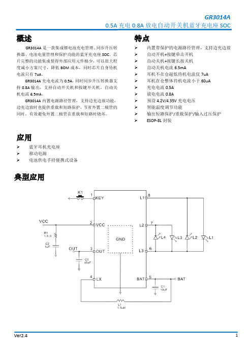
概述GR3014A 是一款集成锂电池充电管理、同步升压转换器、电池电量管理和保护功能的蓝牙充电座SOC 。
芯片完整的功能集成使得外部应用元件极少,可以很大程度减小方案尺寸,降低BOM 成本,同时芯片自身待机电流只有7uA 。
GR3014A 充电电流为0.5A ,同时同步升压转换器支持0.8A 输出,支持自动开关机和按键开关机,自动关机电流6.5mA 。
GR3014A 内置电源路径管理,支持边充边放功能,边充边放时也提供重载和短路保护,节省外置二极管的同时,有效避免外置二极管在重载和短路时烧坏。
应用蓝牙耳机充电座 移动电源电池供电手持便携式设备特点内置带保护的电源路径管理,支持边充边放 自动开机+按键单击开机 自动关机+按键长按关机 自动关机电流6.5mA耳机不在仓超低待机电流仅7uA 耳机在仓整体待机电流小于60uA 充电电流0.5A 放电电流0.8A预设4.2V/4.35V 充电电压智能温度调节功能输出短路保护/重载保护/输入过压保护ESOP-8L 封装典型应用管脚信息(ESOP8)管脚描述绝对最大额定值注:绝对最大额定值是指超出该范围芯片可能会损坏,如无特殊说明所以电压值都是以GND为参考。
电气特性无特殊说明,VIN=5V,Ta=25℃符号参数测试条件最小值典型值最大值单位T OTP恒温模式结温120℃I L LED显示驱动电流BAT=3.7V 1.5mA 充电部分VCC VCC电源电压 4.55 5.5V VCC OVP VCC过压保护电压6V VCC OVP_REC VCC过压恢复电压 5.8VI CHG恒流充电电流V BAT=3.8V0.450.50.55AI TRK涓流充电电流V BAT=2.6V80100120mAI FULL BAT截止充电电流80100120mAV BAT预设充电电压GR3014A 4.158 4.2 4.242V GR3014AH 4.3 4.35 4.4V△V RECHRG再充电阈值电压V BAT-V RECHRG150mV V TRK涓流充电阈值电压 2.95V V TRK_HYS涓流充电迟滞电压150mV R ON_P VCC到OUT路径内阻730mΩ放电部分V UV_BAT BAT开启电压V BAT上升 3.2V V BAT_SD BAT关机电压 2.9V BAT OVP BAT过压保护电压 5.1V BAT OVP_REC BAT过压恢复电压 4.9V V BAT_LOW BAT低电提示电压 3.1VI SDBY_BAT1BAT待机电流1V BAT=4.2V,耳机不在仓7uAI SDBY_BAT2BAT待机电流2V BAT=4.2V,耳机在仓整体电流60uAT ON_MIN最小导通时间150nSD MAX最大占空比90%F OP Boost工作频率0.81 1.2MHzV OUT升压输出电压I LOAD=0.5A 4.8 5.0V 5.2V V OUT_OVP输出电压过压保护 5.2V V V OCP输出短路保护电压 3.0V T OCP输出短路保护延时400uS V HL输出重载保护电压 4.2V T HL输出重载保护延时8mSI LOAD_DET最小负载识别电流15uAI OUT_OFF自动关机负载电流BAT=3.7V,C OUT=10uF 6.5mAT SD输出无负载关机延时16SI KEY按键上拉电流BAT=3.7V40uAT KEYS短按按键时间0.5S T KEYL长按按键时间2S应用说明开关机GR3014A可以自动检测负载接入并开机,当负载电流小于6.5mA时延时16S后自动关机;同时也支持按键单击开机和长按关机,单击时按键时间须小于500mS,长按时按键时间须大于于2S。
MSL-239SW-3014

ApprovedCheckedInspecterCheckedPreparedCustomer Maker CUSTOMER NAME MODEL NAME CUSTOMER P/NO.APPROVED DATEApproval SheetPART NUMBER SMD LED MSL-239SW-PUnity Opto Technology Co., Ltd.10F, No.88-8, Sec. 1, Kuang-Fu Rd.,Sanchung City 24158, Taipei, Taiwan.TEL : 886-2-29993988 FAX : 886-2-29993910洸子其科技是一家从事发光二极管产品研发、生产及销售公司,致力于为国内国际市场提供高品质,低成本的各类发光管。
主营产品有:SMD LED 0402、0603、0802、0805、1204、1206、3528、5050、3020、3014、2835、3535、335、020、正面发光及侧面发光,红、绿、蓝、白、黄、橙、粉红、紫、单色双色及三色等…主要应用:照明灯具、灯光亮化装饰工程、玩具礼品、背光显示、荧光验证防伪、手机、家电、MP3、手电筒、汽车、圣诞树、霓虹灯等…点击进入洸子其科技MSL-239SW-P06/24/2009Featuresz Package : Rectangle white 3.0 * 1.4mm P-LCC-2 package with silicone resin.z Feature of the device : Extremely wide viewing angle.Ideal for backlighting and coupling in light guides.z White color : x / y coordinate is 0.28 / 0.28.z Viewing angle : Lambertian Emitter ( 110o).z Technology : InGaN.z Grouping parameter : Luminous Intensity.z Assembly methods : Suitable for all SMT assembly methods.z Soldering methods : Reflow soldering.z Taping : 8-mm tape with 2000 pieces / reel, φ180mm.z Lead free product : RoHS compliant.Applicationsz Automotive : Dashboards.z Backlighting : LCDs, Key pads, Advertising.z Lighting : Signal, symbol and marker lights;Substitution of micor incandescent lamps.z Displays : Indoor and outdoor signboards, message boards.z Status indicators : Industrial electronics.Technical DataUnity Opto Technology Co., Ltd.ALLEDsPreliminary SpecPackage DimensionsNotes :1.All dimensions are in millimeters.2.Tolerance is ± 0.10 mm unless otherwise noted.Recommend Solder PadUnit: mmMethod of Taping / Polarity and Orientation : Packing unit 2000 pieces / reelNotes :1.All dimensions are in millimeters.2.Tolerance is ± 0.20 mm unless otherwise noted.AnodeCathodeCathodeAnodeLuminous intensity is tested at a current pulse duration of 3 ms and an accuracy of +/- 10%.x y Min.Typ.Max.Typ.Typ.3.03.33.50.2800.280Voltage groups are tested at a current pulse duration of 3 ms and an accuracy of +/- 0.05V.Chromaticity coordinate groups are tested at a current pulse duration of 100 ms and a tolerance of ±0.01.Absolute Maximum RatingsSymbol UnitT OP oC T stg o C T j oCI F mA V R V P tot mW ESDVMax.50Reverse Current I R (µA) @ V R = 5V Electrostatic Discharge(HBM)±1K1600WhiteMSL-239SW-PChromaticity Coordinates (Typ.)ForwardVoltage Yellowish siliconeStorage Temp. range Viewing 2θ1/2@ 20mAIntensity I V (mcd) @ 20mA110Selection GuideColor of the Light EmittingAreaPart NumberColor ofEmissionLuminous Parameter Operating Temp. range -30 ~ +85-40 ~ +100Value MSL-239SW-PV F (Volts)Part Number@I F = 20mA120Power dissipation Junction temperature Forward current Reverse Voltage 511030Reflow Soldering Profile Lead SolderLead Free SolderBinAABLAABHAACLAACHABALABAHABBLABBHABCLABCHABDL ABDHBAALBAAHBABLBABHx y x y x y x yA 0.2800.2800.2800.2900.2900.3000.2900.290C 0.2800.2600.2800.2700.2900.2800.2900.270D 0.2800.2500.2800.2600.2900.2700.2900.260E 0.2900.2900.2900.3000.3000.3100.3000.300F 0.2900.2800.2900.2900.3000.3000.3000.290G 0.2900.2700.2900.2800.3000.2900.3000.280H 0.2900.2600.2900.2700.3000.2800.3000.270Min Max K 0.3000.3000.3000.3100.3100.3200.3100.310 2.9 3.0L 0.3000.2900.3000.3000.3100.3100.3100.300 3.0 3.1M 0.3000.2800.3000.2900.3100.3000.3100.290 3.1 3.2N 0.3000.2700.3000.2800.3000.2800.3000.270 3.2 3.3P 0.2800.2900.2800.3000.2900.3100.2900.300 3.3 3.4Q 0.2900.3000.2900.3100.3000.3200.3000.310 3.4 3.5R 0.3000.3100.3000.3200.3100.3300.3100.320 3.5 3.6S 0.2700.2700.2700.2800.2800.2900.2800.280 3.6 3.7T 0.2700.2600.2700.2700.2800.2800.2800.270 3.7 3.8U 0.2700.2500.2700.2600.2800.2700.2800.260 3.8 4.0V 0.2700.2400.2700.2500.2800.2600.2800.250W 0.2900.3100.2900.3200.3000.3300.3000.320X 0.3000.3200.3000.3300.3100.3400.3100.330Chromaticity coordinate groups are tested at a current pulse duration of 100 ms and a tolerance of ±0.01.1850Luminous Intensity Group ( mcd ) @ I F =20mA1550160016001650Max Min 1650Unity Bin CodesMSL-239SW-PABCHC3Bin Code 185019001950Color Coordinate @ I F =20mALuminous intensity is tested at a current pulse duration of 3 ms and an accuracy of +/- 10%.2000321Forward Voltage ( V ) @ I F =20mABin 089Voltage groups are tested at a current pulse duration of 3 ms and an accuracy of +/- 0.05V.45671200125012501300130013501350140014001450145015001500155019001950170017001800175017501800x y x y x y x y A 0.2800.2800.2800.2900.2900.3000.2900.290A10.2800.2850.2800.2900.2850.2950.2850.290A20.2850.2900.2850.2950.2900.3000.2900.295A30.2800.2800.2800.2850.2850.2900.2850.285A40.2850.2850.2850.2900.2900.2950.2900.290B 0.2800.2700.2800.2800.2900.2900.2900.280B10.2800.2750.2800.2800.2850.2850.2850.280B20.2850.2800.2850.2850.2900.2900.2900.285B30.2800.2700.2800.2750.2850.2800.2850.275B40.2850.2750.2850.2800.2900.2850.2900.280C 0.2800.2600.2800.2700.2900.2800.2900.270C10.2800.2650.2800.2700.2850.2750.2850.270C20.2850.2700.2850.2750.2900.2800.2900.275C30.2800.2600.2800.2650.2850.2700.2850.265C40.2850.2650.2850.2700.2900.2750.2900.270D 0.2800.2500.2800.2600.2900.2700.2900.260D10.2800.2550.2800.2600.2850.2650.2850.260D20.2850.2600.2850.2650.2900.2700.2900.265D30.2800.2500.2800.2550.2850.2600.2850.255D40.2850.2550.2850.2600.2900.2650.2900.260E 0.2900.2900.2900.3000.3000.3100.3000.300E10.2900.2950.2900.3000.2950.3050.2950.300E20.2950.3000.2950.3050.3000.3100.3000.305E30.2900.2900.2900.2950.2950.3000.2950.295E40.2950.2950.2950.3000.3000.3050.3000.300F 0.2900.2800.2900.2900.3000.3000.3000.290F10.2900.2850.2900.2900.2950.2950.2950.290F20.2950.2900.2950.2950.3000.3000.3000.295F30.2900.2800.2900.2850.2950.2900.2950.285F40.2950.2850.2950.2900.3000.2950.3000.290G 0.2900.2700.2900.2800.3000.2900.3000.280G10.2900.2750.2900.2800.2950.2850.2950.280G20.2950.2800.2950.2850.3000.2900.3000.285G30.2900.2700.2900.2750.2950.2800.2950.275G40.2950.2750.2950.2800.3000.2850.3000.280H 0.2900.2600.2900.2700.3000.2800.3000.270H10.2900.2650.2900.2700.2950.2750.2950.270H20.2950.2700.2950.2750.3000.2800.3000.275H30.2900.2600.2900.2650.2950.2700.2950.265H40.2950.2650.2950.2700.3000.2750.3000.270K 0.3000.3000.3000.3100.3100.3200.3100.310K10.3000.3050.3000.3100.3050.3150.3050.310K20.3050.3100.3050.3150.3100.3200.3100.315K30.3000.3000.3000.3050.3050.3100.3050.305K40.3050.3050.3050.3100.3100.3150.3100.310L 0.3000.2900.3000.3000.3100.3100.3100.300L10.3000.2950.3000.3000.3050.3050.3050.300L20.3050.3000.3050.3050.3100.3100.3100.305L30.3000.2900.3000.2950.3050.3000.3050.295L40.3050.2950.3050.3000.3100.3050.3100.300M 0.3000.2800.3000.2900.3100.3000.3100.290M10.3000.2850.3000.2900.3050.2950.3050.290M20.3050.2900.3050.2950.3100.3000.3100.295M30.3000.2800.3000.2850.3050.2900.3050.285M40.3050.2850.3050.2900.3100.2950.3100.290N 0.3000.2700.3000.2800.3100.2900.3100.280N10.3000.2750.3000.2800.3050.2850.3050.280N20.3050.2800.3050.2850.3100.2900.3100.285N30.3000.2700.3000.2750.3050.2800.3050.275N40.3050.2750.3050.2800.3100.2850.3100.280P 0.2800.2900.2800.3000.2900.3100.2900.300P10.2800.2950.2800.3000.2850.3050.2850.300P20.2850.3000.2850.3050.2900.3100.2900.305P30.2800.2900.2800.2950.2850.3000.2850.295P40.2850.2950.2850.3000.2900.3050.2900.300Q 0.2900.3000.2900.3100.3000.3200.3000.310Q10.2900.3050.2900.3100.2950.3150.2950.310Q20.2950.3100.2950.3150.3000.3200.3000.315Q30.2900.3000.2900.3050.2950.3100.2950.305Q40.2950.3050.2950.3100.3000.3150.3000.310R 0.3000.3100.3000.3200.3100.3300.3100.320R10.3000.3150.3000.3200.3050.3250.3050.320R20.3050.3200.3050.3250.3100.3300.3100.325R30.3000.3100.3000.3150.3050.3200.3050.315R40.3050.3150.3050.3200.3100.3250.3100.320S 0.2700.2700.2700.2800.2800.2900.2800.280S10.2700.2750.2700.2800.2750.2850.2750.280S20.2750.2800.2750.2850.2800.2900.2800.285S30.2700.2700.2700.2750.2750.2800.2750.275S40.2750.2750.2750.2800.2800.2850.2800.280T 0.2700.2600.2700.2700.2800.2800.2800.270T10.2700.2650.2700.2700.2750.2750.2750.270T20.2750.2700.2750.2750.2800.2800.2800.275T30.2700.2600.2700.2650.2750.2700.2750.265T40.2750.2650.2750.2700.2800.2750.2800.270U 0.2700.2500.2700.2600.2800.2700.2800.260U10.2700.2550.2700.2600.2750.2650.2750.260U20.2750.2600.2750.2650.2800.2700.2800.265U30.2700.2500.2700.2550.2750.2600.2750.255U40.2750.2550.2750.2600.2800.2650.2800.260V 0.2700.2400.2700.2500.2800.2600.2800.250V10.2700.2450.2700.2500.2750.2550.2750.250V20.2750.2500.2750.2550.2800.2600.2800.255V30.2700.2400.2700.2450.2750.2500.2750.245V40.2750.2450.2750.2500.2800.2550.2800.250W 0.2900.3100.2900.3200.3000.3300.3000.320W10.2900.3150.2900.3200.2950.3250.2950.320W20.2950.3200.2950.3250.3000.3300.3000.325W30.2900.3100.2900.3150.2950.3200.2950.315W40.2950.3150.2950.3200.3000.3250.3000.320X 0.3000.3200.3000.3300.3100.3400.3100.330X10.3000.3250.3000.3300.3050.3350.3050.330X20.3050.3300.3050.3350.3100.3400.3100.335X30.3000.3200.3000.3250.3050.3300.3050.325X40.3050.3250.3050.3300.3100.3350.3100.330Color Coordinate @ I F =20mA4Bin Code123REEL DimensionsCarrier Tape Items RemarksSpecificationsLeaderCover TapeCover tape shall be longer than 400mm without carrier tapeThere shall be more than 40 emptiesThe end of the carrier tape shall be adhered on the cover tapeThe orientation of tape shall be as shownThe end of the tape shall be inserted into a slit of the hubThere shall be more than 40 emptiesTrailerSurface Mount Moisture Sensitivity Specifications1. Controlling MoistureUnity Opto Technology, in its design of packing materials and packing methods, takes into consideration the susceptibil some Unity packages to moisture induced damage. The risk of this damage is caused when the LED lens plastic encaps material is exposed to increases or decreases in the Relative Humidity of the surrounding environment.Such damage may include delamination between the die and the LED lens plastic encapsulation material, which may res open connections due to broken wire bonds. Moisture in the package having reached a critical level will fracture the pac in order to escape when exposed to peak temperature conditions, typical in soldering practices.Therefore, the control of moisture levels in the LED package is critical to reduce the risk of moisture-induced failures. P follow JEDEC-STD-033A standards for handling moisture sensitive devices.2. Packaging SMD devices:Unity packages all SMD devices into dry pack bags (moisture barrier bags).Unity includes a desiccant pouch in each bag. Testing confirms that the desiccant pouch greatly reduces the presence of moisture by maintaining the environment in the bag, thus protecting the devices during shipment and storage.3. Handling Dry Packed PartsUpon receipt, the bags should be inspected for damage to ensure that the bag’s integrity has been maintained. Inspectio should verify that there are no holes, gouges, tears, or punctures of any kind that may expose the contents of the bag.To open the bag, simply cut across the top of the bag as close to the original seal as possible being careful not to damage contents. Once open the desired quantity of units should be removed and the bag resealed. If the bag is left open longer 2 hours, the desiccant pouch should be replaced with a dry desiccant and the bag should be sealed immediately to avoid moisture damage.Package LabelCUSTOMER:CUSTOMER P/N:DEVICE TYPE:MSL-239SW-PBIN:ABCH-C-3LOT NO:Q'TY:2000BATCH:MADE IN TAIWANSilicone Product Surface Mount Technology Note1. Pick and Place Nozzle SizeNote: Nozzle's inner Diameter should large than1.2 mm2. Handling PrecautionA. Do not touch the silicone surface and poke with sharp object.B. Do not stack the PCB assembled with LEDs.C. It must hold the LED body only by plastic tweezers, when you take out the LED.。
led3014贴片规格书

3.0mm SMD Hyper White Top LED 3.0mm 贴片超亮白色发光二极管Features 特征•Package Size:3.0(L)×1.4(W)×0.8(T)mm 封装尺寸: 3.0(长)×1.4(宽)×0.8(厚)mm •Silicone Packed 采用硅胶封装•Super long lifetime 超长寿命•Anti UV 防紫外线•White colors are available in(2200K-12000K)可供白光(2200K-12000K)•High CRI products 高显色性产品•Wide viewing angle (2θ1/2=120°)宽角度(2θ1/2=120°)Applications •产品应用•Indoor lighting:Fluorescent lamp,tube •室内照明:日光灯管、灯条•Commercial illumination and displays:•商业照明显示:广告字、广告灯箱Advertising words,light box •LCD Backlighting •LCD背光源•Decorative lighting:light strip •装饰照明:柔性灯条•Automotive interior auxiliary lighting •Other illumination and displays •其它照明和显示类O OBin Range of CRI 显色性等级代码(at I F =30mA,T a =25OC )Top View 顶视Back View 底视Bin Range of Luminous Intensity显指等级代码(T=25O C)a(Luminous flux luminous intensity for the corresponding reference以上光强对应的光通量仅供参考)F a Array=25O C)Bin Range of Luminous Intensity电压等级代码(Ta(Luminous flux luminous intensity for the corresponding reference以上光强对应的光通量仅供参考)Typical Electro-Optical Characteristics Curves 典型光-电特性曲线图PACKAGE OUTLINE 外形尺寸(Units:mm)Recommended Soldering Pattern推荐焊接模式3.00±0.081.400.50G a t e s 9-16r o w sG a t e s 1-8r o w s0.740.70±0.050.80±0.05+-P O L A R I T YP a c k a g e m a r k i n g0.74一、PRECAUTONS IN USE LED/使用LED 注意事项;LED Soldering condition/LED 焊接条件;1:烙铁焊接:烙铁最高30W 尖端温度不超过300℃;焊接时不超过3秒;焊接位至少离胶体2毫米。
EG3014全中文资料

ELECTRONIC GIANT EG3014芯片数据手册大功率MOS管、IGBT管栅极驱动芯片版本变更记录目录1. 特点 (4)2. 描述 (4)3. 应用领域 (4)4. 引脚 (4)4.1. 引脚定义 (4)4.2. 引脚描述 (4)5. 结构框图 (5)6. 典型应用电路 (5)7. 电气特性 (7)7.1 极限参数 (7)7.2 典型参数 (8)7.3 开关时间特性及死区时间波形图 (9)8. 应用设计 (10)8.1Vcc端电源电压 (10)8.2输入逻辑信号要求和输出驱动器特性 (10)8.3自举电路 (11)9. 封装尺寸 (12)9.1 SO8封装尺寸 (12)EG3014芯片数据手册V1.01. 特点⏹高端悬浮自举电源设计,耐压可达100V⏹内建死区控制电路⏹自带闭锁功能,彻底杜绝上、下管输出同时导通⏹采用半桥达林顿管输出结构具有大电流栅极驱动能力⏹专用于无刷电机N沟道MOS管、IGBT管栅极驱动⏹HIN输入通道高电平有效,控制高端HO输出⏹LIN输入通道高电平有效,控制低端LO输出⏹外围器件少⏹静态电流小:4.5mA⏹封装形式:SOP-82. 描述EG3014是一款高性价比的大功率MOS管、IGBT管栅极驱动专用芯片,内部集成了逻辑信号输入处理电路、死区时控制电路、闭锁电路、电平位移电路、脉冲滤波电路及输出驱动电路,专用于无刷电机控制器中的驱动电路。
EG3014高端的工作电压可达100V,Vcc的电源电压范围宽可达30V,静态功耗低仅4.5mA。
该芯片具有闭锁功能防止输出功率管同时导通,输入通道H IN和L IN内建了一个10K下拉电阻,在输入悬空时使上、下功率MOS管处于关闭状态,输出结构采用半桥式达林顿管结构,采用SOP8封装。
3. 应用领域⏹电动摩托车控制器⏹电动自行车控制器⏹100V降压型开关电源⏹变频水泵控制器⏹无刷电机驱动器⏹高压Class-D类功放4. 引脚4.1. 引脚定义IN IN图4-1. EG3014管脚定义4.2. 引脚描述5. 结构框图H LOGNDVccHOVS VBL图5-1. EG3014结构框图6. 典型应用电路+15V+VinH L OUT图6-1. EG3014典型应用电路图——中、小功率半桥驱动应用+15V+VinH L OUT图6-2. EG3014典型应用电路图——大功率电机场合应用+15V+VinH L OUT图6-3. EG3014典型应用电路图——外接自举二极管应用7. 电气特性7.1 极限参数注:超出所列的极限参数可能导致芯片内部永久性损坏,在极限的条件长时间运行会影响芯片的可靠性。
2835、3014和3528灯珠LED灯管的应用对比

2835贴片优点:1、芯片采用大功率背镀铝工艺,散热更直接2、芯片热量直接从支架底部导出,相对3014散热面积更大,散热性能更加优良3、发光面为长方形,相对3014、3528发光面积大、发光角度大,发光均匀,发光面积是3014的2.3倍,3528的2.1倍 4、2835为升级新光源,应用广泛,克服3014侧面发光角度小的缺点,有效解决3528照明应用中点光源现象5、根据产品型号、客户散热使用条件,可采用20-50毫安多种电流使用6、增加10%的透光率,可采用85-95%的透光罩,在LED 日光灯上体现特别明显7、特殊规格使用,可有效替代5050 2835贴片制造成本高的因素:1、硅胶使用是现有3528胶量的1.4倍,荧光粉为1.7倍2、支架需要镀银的面积大,耗银多,支架厚度为0.3mm ,为现有3528厚度0.15mm 的2倍贴片一:散热方式的区别1. 由于3528灯珠是通过导线把热量传导到负极引脚上去,所以3528灯珠的散热方式也可称为“负极散热”;2. 而2835、3014灯珠是通过通过在灯珠支架上打孔并装上导热片,把芯片的热量直接传导到铝基板上,为了与3528的散热方式区分开来,它的散热方式又称为“热电分离”,意思就是热量与电流不是通过同一根导线来传导的。
下图为3014与2835的实物图片:二. 2835、3014在市场取代3528主要的原因:1. 就是因为它们的封装结构不一样,散热性能更好,能在30mA的电流下正常工作(正常的理解)。
2. 深层次原因,2835、3014成本更好随意控制,猫腻太多,不明?往下看吧!三:3528光源好处:1.LED灯珠3528 现在可以做到7-8lm,单颗灯珠功率是0.0625w,市场价格不含税0.10~0.13元之间(所用LED芯片尺寸、等级不一样,决定了价格的不一样;如芯片用A品,专案品,B 品等,同样是7-8LM的亮度,品质可大不一样,价格当然不一样);所以,现在判断光源的品质,并不是象以前一样,单看LED的亮度,更要看所用LED芯片的等级,A品、专案品或B 品,光源品质上有缺陷,不是一下子就可以显现的,厂家敢用,就是了解大家不容易区别品质,需要时间去证明;2. 灯珠3528 使用时间长,生产工艺、品质相对稳定,亮度也有7-8LM了,主要是成本相对高了点,因为W数小只有0.0625W单颗,要用数量去补W数数。
led规格书4(精)
客户:产品型号:JT.CB328ZA-R8适用于 :顺向电流 IF=20mA目录1. 特性2. 应用范围3. 成品外观尺寸4. 最大绝对标称值5. 光电特性参数6. 典型光电参数曲线7. 编带规格8. 包装方式9. 标签描述10. BIN 级范围11. 可靠度实验项目及条件12. 使用注意事项客户确认批准审核拟制深圳市聚飞光电股份有限公司深圳市宝安区大浪街道高峰社区创艺路 65号Tel:+86-755-29646360Fax:+86-755-296322851、特性:1.1封装尺寸:3.5x2.8x1.9mm1.2发光颜色:白色 (高显色 1.3发光类型:单色型 1.4焊接方式:回流焊 1.5符合RoHS 标准2、应用范围:2.1闪光灯 2.2LCD背光 2.3室内照明 2.4灯饰照明3、成品外观尺寸:备注:1.所有尺寸均以 mm 为单位2.在没有明确标注的情况下,公差均为 ±0.10mm4、最大绝对标称值 (环境温度 =25℃ :参数缩写标称值单位消耗功率 Pd 100mW 顺向电流 I F 30mA 顺向峰值电流*1I FP 100mA 反向电压 VR 5.0V焊接温度 Tsol 回流焊:245℃,10sec. 手工焊:300℃,3sec.使用温度 Topr -35℃~+85℃储存温度 Tstg -40℃~+85℃*I FP 条件:脉宽≤0.1msec, 周期≤1/105、光电特性参数 (环境温度 =25℃ :参数缩写最小值典型值最大值单位条件顺向电压 Vf 2.9-3.5V I F =20mA 亮度 Iv -2200mcd发光角度2θ1/2-120-deg显色指数 Ra 78-90-反向电流IR 0.5μAVR=5V 备注 :1. 亮度偏差:±5%2. 电压偏差:±0.03V6、典型光电参数曲线:7、编带规格:(单位:mm 包装数量:2000pcs/卷8、包装方式:(单位:mm标签防静电、防潮铝箔袋深圳市聚飞光电股份有限公司 01.JT.CB328ZA-R8 9、标签描述:产品型号产品 BIN 生产日期生产批次 RoHS 标签数量生产批次检验盖章 BIN 级描述: x / x / x-x 正向电压 BI N 级色区 BI N 级亮度 BI N 级如 BI N : 11 /E / 7- 1 : 11 代表亮度 BIN 级,E 代表色区 BIN 级,7-1 代表正向电压 BIN 级 BI 10、BI N 级范围: ( 测试设备:CAMMA 标准机与远方 PMS-80 亮度 IV 与光通量 (公差:±5% @If=20mA: BI N 代码 IV 最小值 (m c d IV 最大值 (m c d 光通量 ( lm 10 1900 2000 6.0~6.4 11 2000 2140 6.4~6.8 11B 2140 2300 6.8~7.4 12 2300 2500 7.4~8.0 13 2500 2800 8.0~9.0 正向电压 VF (公差:±0.03V @ If=20mA: BI N 代码最小值 (v 6- 1 2.9 6- 2 3. 0 7- 1 3. 1 7- 2 3. 2 8- 1 3. 3 8- 2 3. 4 色度坐标(公差:±0.005 @ If=20mA 正白光色区 V 色温 5300K~ 5650K x 坐标 0.3378 0.33 0.33 0.337 y 坐标 0.3589 0.3513 0.3219 0.3278 色区 T 色温 5650K~ 6000K x 坐标 0.33 0.3215 0.3238 0.33 y 坐标0.3513 0.343 0.3165 0.3219 Ver. A5 Page 6 of 10 最大值 (v 3. 0 3. 1 3. 2 3. 3 3. 4 3. 5深圳市聚飞光电股份有限公司 01.JT.CB328ZA-R8 X 6500K~ 7000K 0.3130.3045 0.3092 0.3159 x 坐标 0.3848 0.3723 0.3645 0.3718 偏黄 x 坐标 0.4711 0.4538 0.438 0.4533 0.4538 0.4342 0.4208 0.438 0.4342 0.4189 0.4074 0.4208 0.3347 0.3265 0.304 0.3098 y 坐标 0.3979 0.3879 0.3461 0.3501 W 6000K~ 6500K 0.3215 0.3130.3159 0.3238 x 坐标 0.3723 0.3593 0.355 0.3645 偏红 x 坐标 0.4533 0.438 0.42130.434 0.438 0.4208 0.4071 0.4213 0.4208 0.4074 0.3959 0.4071 0.343 0.3347 0.3098 0.3165 y 坐标 0.3879 0.3775 0.3407 0.3461 自然光色区 L X/Y 参数设定色温4000K~ 4250K 色区 M 色温 4250K~ 4600K 暖白光色区 X/Y 参数设定色温 2850~ 3000k y 坐标 0.4424 0.4371 0.4045 0.4095 0.4371 0.4295 0.3974 0.4045 0.4295 0.4206 0.3907 0.3974 色区 D1 色温 2850K~ 3000k y 坐标 0.4095 0.4045 0.37 0.3747 0.40450.3974 0.3648 0.37 0.3974 0.3907 0.3607 0.3648 C1 C2 3000~ 3250k D2 3000K~ 3250kE 3250K~ 3500kF 3250K~ 3500k CIE 1931: 0.48 0.46 0.44 0.42 0.40 4250K 4000K 4500K 5300K 5650K 6000K 6500K 7000K 3500K CIE 1931 (x,y diagram 3000K 3250K 2850K E D2 C2 D1 C1 BBL 0.38 0.36 0.34 0.32 0.30 0.28 0.26 0.28 0.30 0.32 0.34 L M F T X W V 0.36 0.38 0.40 0.42 0.44 0.46 0.48 0.50 0.52 Ver. A5 Page 7 of 10深圳市聚飞光电股份有限公司 01.JT.CB328ZA-R8 11、可靠度实验项目及条件: 序号 1 测试项目寿命实验高温高湿 (静态实验冷热冲击高温储存低温储存温度循环回流焊测试条件测试电流:20mA 温度:25℃测试时间:1000 小时温度:=+65℃湿度:90% RH 测试时间:240 小时 -40℃~+100℃ 20min 10s 20min 测试时间:100 个循环高温:100℃测试时间:1000 小时低温:-40℃测试时间:1000小时 -40℃ ~ +100℃ 60min 20min 60min 测试时间:20 个循环 245℃(Max.,最大不超过 10 秒钟样品数量 20 允收/拒收 0/1 2 20 0/1 3 4 5 6 7 20 20 20 20 20 0/1 0/1 0/1 0/1 0/1 可靠度实验不合格判定标准: ·Iv:衰减超过 30% ·Vf:变化超过 20% 备注:1、同一项实验结果的测试需在 2 个小时之内完成; 2、测试必须在每项实验完成后、材料恢复正常环境条件下才能进行. 12、使用注意事项: 请参照《聚飞光电--LED 使用说明书》 Ver. A5 Page 8 of 10。
欧司朗LED规格书
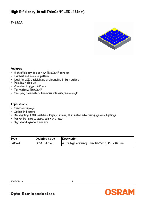
F4152AHigh Efficiency 40 mil ThinGaN ®LED (455nm)2007-09-131Features •High efficiency due to new ThinGaN ® concept •Lambertian Emission pattern•Ideal for LCD backlighting and coupling in light guides •Polarity: n-side up•Wavelength (typ.): 455 nm •Technology: ThinGaN ®•Grouping parameters: luminous intensity, wavelengthApplications •Outdoor displays •Optical indicators•Backlighting (LCD, switches, keys, displays, illuminated advertising, general lighting)•Marker lights (e.g. steps, exit ways, etc.)•Signal and symbol luminaireType Ordering Code DescriptionF4152AQ65110A704040 mil high efficiency ThinGaN ® chip, 450 - 465 nmElectrical values1)(T A = 25 °C)Parameter Symbol Value2)Unitmin.typ.max. Dominant wavelengthI F = 350 mA, pulsedλdom450465nm Reverse voltageI R = 10µAV R10VForward voltageI F = 350 mA, pulsed VF2.73.8VRadiant PowerI F = 350 mA, pulsedΙV32 a.u.1)Measurement limits describe actual settings and do not include measurement uncertainties. Each wafer and fragmentof a wafer is subject to final testing. The wafer or its pieces are individually attached on foils (rings). All el. values are referenced to the vendor's measurement system (correlation to customer product(s) is required). Measurement uncertainty +/-15% for brightness, +/- 1nm for wavelength and +/- 0.1V for voltage.2)Due to the special conditions of the manufacturing processes of LED, the typical data or calculated correlations oftechnical parameters can only reflect statistical figures. These do not necessarily correspond to the actual parameters of each single product, which could differ from the typical data and calculated correlations or the typical characteristic line. If requested, e.g. because of technical improvements, these typ. data will be changed without any further notice.2007-09-1322007-09-133Binning Maximum Ratings 1)Radiant Power 450 - 455 nm455 - 460 nm460 - 465 nm28.0 - 35.2 a.u.A1B1C135.2 - 41.2 a.u.A2B2C241.2 - 48.4 a.u.A3B3C348.4 - 56.8 a.u.A4B4C4> 56.8 a.u.A5B5C5ParameterSymbol Value Unit Maximum Operating temperature range T op -40...+100°C Maximum forward current (T A = 25°C)I F 700mA Minimum forward current (T A = 25°C)I F100mA Maximum surge Current (T A = 25°C)t p = 10 µs, D = 0.05I peak0.7A Maximum junction temperatureT j125°C1)Maximum ratings are strongly package dependent and may differ between different packages. The values given represent the chip in an OSRAM Opto Semiconductor’s Platinum Dragon® package.Mechanical values1)Parameter Symbol Value2)Unitmin.typ.max.Length of chip edge (x-direction)L x0.95 1.00 1.05mm Length of chip edge (y-direction)L y0.95 1.00 1.05mm Diameter of the wafer D50.8mmDie height H170190210µm Diameter of bondpad d130150170µm Additional informationMetallization frontside Gold partialMetallization backside AuDie bonding Epoxy bonding1)All chips are checked according to the following procedure and the OSRAM OS specification of the visual inspectionA63501-Q0013-N001-*-76G3:Unless otherwise described below, the quality level of the final visual inspection shall comply to an AQL 0,4 (according MIL-STD-105D, level II), if the customer performes an incoming visual inspection of a shipment. The quality inspection (final visual inspection) is performed by production. An additional visual inspection step as special release procedure by QM after the final visual inspection is not installed.2)Due to the special conditions of the manufacturing processes of LED, the typical data or calculated correlations oftechnical parameters can only reflect statistical figures. These do not necessarily correspond to the actual parameters of each single product, which could differ from the typical data and calculated correlations or the typical characteristic line. If requested, e.g. because of technical improvements, these typ. data will be changed without any further notice2007-09-1342007-09-135Chip OutlinesDimensions are specified as typicalvalues as follows: mm (inch).Published by OSRAM Opto Semiconductors GmbH Wernerwerkstrasse 2, D-93049 Regensburg © All Rights Reserved.Attention please!The information generally describes the type of component and shall not be considered as assured characteristics or detailed specification.Terms of delivery and rights to change design reserved. Due to technical requirements components may contain dangerous substances. For information on the types in question please contact our sales organization.Handling and Storage Conditions:Storage time for wafers in sealed condition shall not exceed 6 months (storage ambient conditions: Ta=15...30°C;relative humidity: < 60%).The hermetically sealed shipment lot shall be opened under temperature and moisture controlled cleanroom environment only. Customer has to follow the according rules for disposition of material that can be hazardous for humans and environment. Dice have to be handled ESD sensitive.PackingChips are placed on a blue foil with minimum size of 18 x 18 cm².For shipment the wafers of a shipment lot are arranged to stacks. The stack is put in a plastic ESD bag with a maximum of 14 wafers in one bag. A maximum of 4 bags is put in a packaging box. A maximum of 5 packaging boxes is put in a shipping carton which is sealed for storage and shipment.Please use the recycling operators known to you. We can also help you – get in touch with your nearest sales office. By agreement we will take packing material back, if it is sorted. You will have to bear the costs of transport. For packing material that is returned to us unsorted or which we are not obliged to accept, we shall have to invoice you for any costs incurred.Label and shipping documentsEach wafer is identified with a sticker, which is attached to each wafer. The label shows chip type, wafer number, quantity, binning and the minimum, average and maximum values of voltage, luminous intensity and wavelength. Each wafer shipment includes an additional document, which summarizes the content.Design objectives a) workabilityThe chip design was developed and released based on the the vendor’s standard assembly procedures and packaging. Bond strength properties are in accordance to MIL_STD-750D, method 2037. Whether the chip fits to the customer’s product(c) with its according die and wire bond procedures and packaging must be evaluated by the customer himself. If workability problems arise after this release a mutually conducted problem solving procedure has to be set up, if thechips are suspected of contributing to the problemsb) chip characteristicsThe chips are produced by the vendor with best effort, but on chip level a subset of the chip characteristics can be determined only. Performance of the chip in the customer’s product(s) can only be determined by the customer himself. Returns/ComplaintsTo return material because of technical or logistical reasons a RMA-number is necessary. Samples for analysis purposes can be send to OSRAM OS without credit.Shipping Conditions:If not otherwise arranged, the “General Conditions for the supply of products and services of the electrical and electronics industry” apply for any shipment. If these documents are not familiar to you, please request them at our nearest sales office.Components used in life-support devices or systems must be expressly authorized by us for such purpose! Critical components2), may only be used in life-support devices or systems3) with the express written approval of OSRAM OS.1) Typical (refered to as typ.) data are defined as long-term production mean values and are only given for information. This is not a specified value.2)A critical component is a component used in a life-support device or system whose failure can reasonably be expected to cause the failure of that life-support device or system, or to affect its safety or effectiveness of that device or system.3)Life support devices or systems are intended (a) to be implanted in the human body, or (b) to support and/or maintain and sustain human life. If they fail, it is reasonable to assume that the health of the user may be endangered.2007-09-136。
3014贴片灯珠

3014贴片灯珠具体规格参数如下:
1. 【产品名称】:LED3014贴片
2. 【电压】:
3.0-3.2V
3. 【电流】:30MA
4. 【功率】:0.1W
5. 【产品尺寸】:3.0*1.4*1.2MM
6. 【芯片厂家】:三安
7. 【亮度】:10-12LM 11-13LM
8. 【色温】:2800-3200K 4000-4500K 6000-6500K 11000-13000K
9. 【使用寿命】:>50,000个小时
产品特征:发光角度大,广泛应用于日光灯、面板灯、球泡灯、吸顶灯、天花灯、背光、指示产品等
主要材质:硬硅胶封装(进口日本信越=保证低光衰,防硫化)金线焊接(北京达博=纯金99.99%金线焊接)
特点:体积小、角度大,亮度高、低电压驱动
包装:真空包装4000/PCS/盘
焊接方法:适应于所有的SMT贴片式焊接。
产品应用:手机按键灯、车载指示灯、仪器仪表指示灯、手机背光源、LED显示屏、MP3背光源、液晶显示屏,背光源、户外看板、背光源产品、电器产品指示、汽车仪表、影音设备、车载DVD、智能水表、电表。
MP3、MP4、MP5、蓝牙、特种照明、交通信号灯、室内照明、工业照明、广告语标示等。
台湾光宝3014 LED灯珠规格书
0.400
Y-coordina te
4500K S1 S3 S5
T1
Q5
0.380
T2
S4 S6
S2
Q6
0.360
0.340 0.360 0.370 0.380 0.390 0.400 0.410
X-coordina te
Tolerance on each Hue (x, y) bin is +/- 0.01.
: : :
2010/04/20 Version : A 0 of 12
LITE-ON
TECHNOLOGY
CORPORATION
Property of Lite-On Only Features
* * * * * * Package in 8mm tape on 7" diameter reels. Compatible with automatic placement equipment. Compatible with infrared and vapor phase reflow solder process. EIA STD package. I.C. compatible. Meet green product and Pb-free(According to RoHS)
Package Dimensions of Tape
Note: 1. All dimensions are in millimeters
Part No. : LTW-M140VNS40 BNS-OD-C131/A4
Page :
8
of
12
LITE-ON
TECHNOLOGY
CORPORATION
米一体日光灯7W规格书

●64 PCS3014 7W T5一体LED日光灯管1) 采用高亮度芯片封装LED为光源,出光均匀2) 光效80-90LM/W3) 显色指数Ra>80,散热好,光衰小;4) 高导热铝合金外壳,机械强度好散热性能佳5) 电源宽电压输入86-276VAC,恒流输出启动速度快,无频闪,防雷击,带PFC功能;6)清静舒适,没有噪音:7)寿命长:光衰少,寿命长达50000H.8)频繁开关不会导致任何损坏。
9)抗振动性好,便于运输。
➢写字楼➢工厂➢地下停车场➢商场➢学校➢居家照明场所等【二】产品图片【三】产品特点【四】应用场所【五】产品尺寸A B C D E670542212534【六】产品参数电源输入电压(Voltage)86-265Vac消耗功率(Power)7W 频率(Frequency)50/60Hz功率因素(Power factor)>0.92PF 电源效率(Efficiency)>86%显示指数(Show index)>70Ra 色温(Color Temperature)3000-6500K防护等级Protection grade光通量(Flux)620LM±10%平均寿命(Life expectancy)30000-50000H 工作温度(Operating Temperature)-20~+65℃储藏温度(Storage Temperature)-20~+80℃电源驱动方式内置非隔离电源温升<35℃灯具接头(Lamp holder)三头插座尺寸(Size)25*34*570mm 净重(Net weight)180g表面处理氧化亮银LED数量(Quantity)64PCS 3014材质(Material quality)铝型材+铝基板发光角度>120°【七】光通量衰减图【八】平均照度1.5米2米2.5米3米照度值60Lux34Lux22Lux15Lux【九】配光曲线图【十】安装示意图。
台湾AOT灯珠产品规格书3020系列
Symbol IF IFP VR Tj Topr Tstg
ESD PD Tsld
Maximum Value
Unit
30
mA
100
mA
5
V
125
°C
-30 ~ +85
°C
-40 ~ +100
°C
±2000
V
105
mW
Reflow Soldering 260℃,10sec
CD0WW0000-AG00/AG01
Soldering Reflow
-Soldering of the SMD LEDs should conform to the soldering condition in the individual specifications. -SMD LEDs are designed for Reflow Soldering. -In the reflow soldering, too high temperature and too large temperature gradient such as rapid
Wavelength λ (nm)
90 o
0
CD0WW0000-AG00/AG01
Page 7 of 15
Preliminary
Recommended Reflow Soldering Conditions
Surface Mounting Condition
In automatic mounting of the SMD LEDs on printed circuit boards, any bending, expanding and pulling forces or shock against the SMD LEDs should be kept min. to prevent them from electrical failures and mechanical damages of the devices.
E021-V01 Lightbar承认书制作教育训练

客戶對應料號
對應廠內 44皆料號 對應的客戶 客戶對 應料號
5
二. L/B承認書資料作業內容
製作時間 製作時間 客戶對應料號
客戶對應料號
與製作時間一 致,修改者填寫 製作人簽名
注意事項: 此資料有對應客戶廠區Word檔,客戶不同, 對應廠區不同,資料如下:
資料頁次等資 料全部製作OK 再進行修改
6
11
二. L/B承認書資料作業內容
客戶對應料號 廠內打件日 期
注意事項: 1.尺寸數據參考客戶機構圖製作.郵件通知品管人員製作 2.數據由品管提供. 3.數據不能有顯示紅色字體的,且上下規格參照機構.
12
二. L/B承認書資料作業內容
重點尺寸雙邊規格 參照機構製作.
廠內打件日 期
PPK需在1.332.00之間
15
二. L/B承認書資料作業內容
製作時間
客戶對應料號
16
二. L/B承認書資料作業內容
注意事項: 1.RA報告也是固定,跟爐溫曲綫圖區分一致, 分別為FPCA、HB、MNT,區分為: BOM中只有FPC+PCB為HB! BOM中只有FPC為全軟板(FPC)! BOM中只有PCB為MNT! 2.根據不同的型號及客戶提供不同的RA報告!
取樣數固定為 35PCS, 數據不 能顯示紅色字 體,且不能超 出規格 .
此位置需顯示 為“0”,如顯示 其它數據則代 表量測數據有 NG的
注意事項: 1.重點尺寸規格參照機構製作,同全尺寸相同,郵件通知品管人員製作 2. PPK值必需1.33~2.00之间! 3.取樣數固定為35 Pcs.,不可為其它數據!
课程编号 课程名称 CMI新產品導入流程 选用对象 课程目标:让学員了解Lightbar承認書如何製作 教学大约/重点内容 一、 L/B承認書資料製作流程圖 二、 L/B承認書資料作業內容 三、總結 讲授法 PPT檔 教学方法 教学资源
led灯管
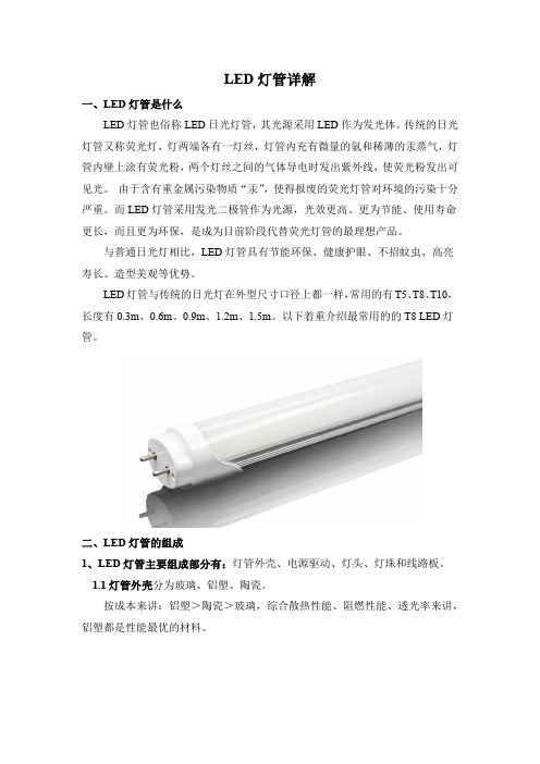
LED灯管详解一、LED灯管是什么LED灯管也俗称LED日光灯管,其光源采用LED作为发光体。
传统的日光灯管又称荧光灯,灯两端各有一灯丝,灯管内充有微量的氩和稀薄的汞蒸气,灯管内壁上涂有荧光粉,两个灯丝之间的气体导电时发出紫外线,使荧光粉发出可见光。
由于含有重金属污染物质“汞”,使得报废的荧光灯管对环境的污染十分严重。
而LED灯管采用发光二极管作为光源,光效更高、更为节能、使用寿命更长,而且更为环保,是成为目前阶段代替荧光灯管的最理想产品。
与普通日光灯相比,LED灯管具有节能环保、健康护眼、不招蚊虫、高亮寿长、造型美观等优势。
LED灯管与传统的日光灯在外型尺寸口径上都一样,常用的有T5、T8、T10,长度有0.3m、0.6m、0.9m、1.2m、1.5m。
以下着重介绍最常用的的T8 LED灯管。
二、LED灯管的组成1、LED灯管主要组成部分有:灯管外壳、电源驱动、灯头、灯珠和线路板。
1.1灯管外壳分为玻璃、铝塑、陶瓷。
按成本来讲:铝塑>陶瓷>玻璃,综合散热性能、阻燃性能、透光率来讲,铝塑都是性能最优的材料。
1.2按电源驱动分为隔离电源和非隔离电源隔离电源:在电源的输入端和输出端中间有隔离变压器,可避免触电,因此成本也要贵。
非隔离电源:负载端与输入端有直接的连接,因此触摸负载就有触电的危险。
一般非隔离电源的绝缘靠线路板的薄膜绝缘,虽然这层薄膜绝缘可以耐2000v高压,但有时螺丝孔的毛刺会产生爬电现象而导致触电。
因此,非隔离电源在安全上存在隐患。
1.3 LED灯管灯头的尺寸与普通日光灯一致,因此可直接替换。
新光源出产的LED铝塑灯管具有可旋转的灯头,性能更加卓越。
1.4 LED灯管的灯珠一般分为3014和2835这两类。
其中3014是指尺寸为3.0(长)×1.4(宽)×0.8(厚)mm的LED灯珠,2835为2.8 (长)×3.5 (宽)×0.8 (厚)mm的LED灯珠。
3014led贴片灯珠规格介绍

3014led贴片灯珠规格介绍
3014led贴片灯珠规格介绍
3014led贴片灯珠是表面贴片发光二极管黄色胶体系列的一种,分为暧白、白灯、商业白、冷白光等。
主要用于户内外显示屏、柔性灯条,辅助照明、背光源等照明。
其特点具备,高亮度表面,发射角可以达到120,特别适合所有表面贴片技术。
3014led贴片灯珠规格要达到好的效果,需要选用优质的原料,具体如下介绍:
1、LED晶片:均经过严格的承认程序,亮度衰减1000hrs <3%(25度环境温度及恒定的温湿度);
2、硅胶:超低光衰
3、金线:选用具高延展性产品,可靠性高;
4、环氧树脂(EPOXY):高TG点,低应力,高透光率,高耐侯性,具良好的抗紫外线性能;
5、支架:镀银层有十足的保障,高精度,良好的导热性;
6、银胶:耐高温,低阻抗,低膨胀,高粘度;
3014led贴片灯珠规格:
1、正向电流=30mA
2、电压=2.0-3.4V 显色指数=60-90
3、光通量=10-14LM
4、功率=0.1W
5、寿命>50000小时
6、尺寸=3.0(长)×1.4(宽)×0.8(厚)mm。
LED背光源3014规格书
The suggestion pick-up head is as same as follow the Sketch Map.
About the downward pressure of Pick-up Head, Please consult the Absolute Maximum Ratings.
45° 60°
75° 90°
60 715.0 90
Radiation Angle
7
Relative Luminosity
Absolute Maximum Ratings
Parameter
Symbol Rating
Reverse Voltage
Vr
5
Forward Current
If
30
Power Dissipation
** The luminous intensity tolerance is ± 7%. *** Life time means that estimated time to 50% degradation of initial luminous intensity.
Life test board information, please refer to appendix II.
Temperature Humidity
No
Items[1]
Other
(℃)
(பைடு நூலகம்)
condition
High temperature
1
100
-----
storage
Criteria for judgment
Hrs Times Sampling LED
Vf @
- 1、下载文档前请自行甄别文档内容的完整性,平台不提供额外的编辑、内容补充、找答案等附加服务。
- 2、"仅部分预览"的文档,不可在线预览部分如存在完整性等问题,可反馈申请退款(可完整预览的文档不适用该条件!)。
- 3、如文档侵犯您的权益,请联系客服反馈,我们会尽快为您处理(人工客服工作时间:9:00-18:30)。
APPROVAL SHEETAOT MODEL NAME 3014FAOT PART NUMBER 3014C-W3M6CUSTOMER NAME CMIDATE 2011/MarchVERSION 1MAKER CUSTOMERPrepared Checked ApprovedAOT HeadquartersNo. 13, Gongye 5th. Road, Hsinchu Industrial Park, Hukou Shiang,Hsinchu Hsien 303, Taiwan, R.O.C.TEL: +886-3-597-6988 / FAX: +886-3-598-7392Revision NoteDate Revision Page Version2011-03-08 Initiate Document 15 1Package OutlineType Number: 3014C-W3M6Unit: mm, Tolerance: ± 0.2 mmItem MaterialsPackage Heat-Resistant PolymerEncapsulating Material Silicone ( with phosphor )Electrode Ag Plating Copper Alloy•Single blue chip.•High brightness SMD.•Compact package outline (LxWxH) of 3.0 mm x 1.4 mm x 0.52 mm.•Compatible with reflow soldering.•Complies with RoHS Directive.Optical/Electronic Characteristics (Ta=25°C)Item Symbol Condition Value Unit Forward Voltage V F I F = 60 mA 2.8 ~ 3.4 V Luminous Flux φV I F =60mA 14 ~ 18.5 lm Reverse Current I R V R=5V≦2.0µA* V F measurement allowance is ±0.05V* Dominant wavelength measurement allowance is ±1nm* Luminous flux is NIST reading. Luminous flux tolerance: ±10%Absolute Maximum Ratings (Ta=25°C)Item Symbol Maximum Value Unit Forward Current I60 mAFPeak Pulse Forward Current; (1kHz,1/10 duty cycle) I100 mAFPReverse Voltage. V5 VRLED Junction Temperature. T j120 °C Operating Temperature. T-30 ~ +85 °CoprStorage Temperature. T-40 ~ +85 °CstgPower Dissipation P204 mWDSoldering Temperature TReflow Soldering 260℃,10secsldGroup Definition of Forward VoltageGroup Definition of BrightnessRank Condition φv(lm) Rank X2075 17.75 ~ 18.50 Rank X2000 17.00 ~ 17.75 Rank X1925 16.25 ~ 17.00 Rank X1850 15.50 ~ 16.25 Rank X1775 14.75~ 15.50 Rank X1700 T a =25oC I F =60mA14.0 ~ 14.7540mA and 60mA Table of Brightness and CIE40mA60mA φv(lm) CIE-x CIE-y φv(lm) CIE-x CIE-y IvxyIv * 1.37x-0.002y-0.002*A shipment shall consist of the LEDs of a combination of different ranks of luminous flux,wavelength and forward voltage. The percentage of each rank in the shipment shall be determined by AOT *The ranking information of LEDs can be found on the reel label.Rank Condition V F (V) L1 2.8 ~ 3.1 L2T a =25oC I F =60mA3.1~3.4Group Definition of Chromaticity CoordinateChromaticity coordinate groups are measured with an accuracy of ±0.01.Optical/Electronic CharacteristicsForward Voltage vs. Forward Current (Ta=25℃)Forward Current vs. Relative Luminous Flux (Ta=25℃)Ambient Temperature vs. Forward Voltage (I FP =60mA)Ambient Temperature vs. Relative Luminous Flux (I FP =60mA)Forward Current vs. Chromaticity Coordinate (Ta=25℃) Ambient Temperature vs. Chromaticity Coordinate (I FP=60mA)Spectrum Radiation PatternSurface Mounting ConditionIn automatic mounting of the SMD LEDs on printed circuit boards, any bending, expanding and pulling forces or shock against the SMD LEDs should be kept min. to prevent them from electrical failures and mechanical damages of the devices.Soldering Reflow-Soldering of the SMD LEDs should conform to the soldering condition in the individual specifications. -SMD LEDs are designed for Reflow Soldering.-In the reflow soldering, too high temperature and too large temperature gradient such as rapid heating/cooling may cause electrical & optical failures and damages of the devices.-AOT cannot guarantee the LEDs after they have been assembled using the solder dipping method. 1) Lead Solder2) Lead-free Solder3) Manual Soldering Conditions- Lead SolderMax. 300 o C for Max. 3sec, and only one time.- Lead-free SolderMax. 350 o C for Max. 3sec, and only one time.- There is possibility that the brightness of LEDs is decreased, which is influenced by heat or ambient atmosphere during reflow. It is recommended to use the nitrogen reflow method.- After LEDs have been soldered, repair should not be done. As repair is unavoidable, a double-head soldering iron should be used. It should be confirmed beforehand whether the characteristics of the LEDs will be damaged by repairing or not.- Reflow soldering should not be done more than two times.Taping and Orientation Quantity: 2,500 pcs/reelItem Spec. Tolerance(mm) Item Spec. Tolerance(mm) W 8.00 ±0.10 P2 2.00 ±0.05E 1.75 ±0.10 t 0.25 ±0.02F 3.50 ±0.05 A0 1.53 ±0.10D0 1.50 +0.10 B0 3.20 ±0.10D10.72 ±0.10 K00.72 ±0.10P0 4.00 ±0.10Packing FormationPackage Outlook302 26725 Metal Bag/1 Carton 62,500 pcs/ 1CartonAntistatic Shielding Metal Bag 1 Reel / Bag Diameter : 178 mm Width : 8 mm 2,500 pcs/Reel Antistatic Reel +5g drying agentLBin(Vf/Iv/CIE) :Vendor PN :3014C-W3M6 SN :a : Customer part numberb : Forward voltage rangec : brightness ranged : CIE range e : min Vf f : max Vfg : min Ivh : max Ivnn : quantity of LEDAYMDxxxx –xxxx : A: AOT, Y: year, M: month, D: day, xxxx-xxx : serial No. SYMDxxxx: S: AOT factory , Y: year, M: month, D: day, xxxx : serial NoPN : aLot No :AYMDxxxx -xxx:Qty :nn EABin(Vf/Iv/CIE) :b-c-dVendor PN :3014C-W3M5SN :SYMDxxxxNo.Test Item Standard Test TestNote Number of1 Steady State Operating Life Internal Ref. I F =20 mATa=25 oC 168 hr 0/20 2 Thermal ShockJESD22-A106-A -40 oC ~ 85 oC Hold 30 min 84 cycles 0/20 3 High TemperatureStorage JESD22-A103-A Ta=125 oC 168 hr 0/20 4 Low TemperatureStorage Internal Ref. Ta=-40 o C 168 hr 0/20 5 High Temperature High Humidity JESD22-A101-B Ta=85 o C RH=85% 168 hr 0/20 6On-Off TestInternal Ref.2 sec ON - 2sec OFF100,000 cycles0/20Criteria for Judging Damage* U.S.L: Upper Standard Level * L.S.L: Lower Standard LevelCriteria for Judgment Item Symbol Test ConditionsMin. Max. Forward Voltage V F I F =140mA - *U.S.L×1.1 Reverse Current I R V R =5V - *U.S.L×2.0 Luminous FluxφVI F =140mA*L.S.L×0.7 -Cautions1. Storage ConditionsBefore opening the package:℃within a The LEDs should be kept at 30 or less and 90%RH or less. The LEDs should be usedyear. When storing the LEDs, moisture proof packaging with absorbent material is recommended.After opening the package:℃ be soldered within The LEDs should be kept at 30 or less and 70%RH or less. The LEDs should168 hours (7days) after opening the package. If unused LEDs remain, they should be stored in moisture proof packages, such as sealed containers with packages of moisture absorbent material.It is also recommended to return the LEDs to the original moisture proof bag and to reseal the moisture proof bag again.If the moisture absorbent material has faded away or the LEDs have exceeded the storage time , baking treatment should be performed using the following conditions.℃Baking treatment : more than 24 hours at 65 ± 5 .AOT LED electrodes are gold plated. The gold surface may be affected by environments which contain corrosive substances. Please avoid conditions which may cause the LED to corrode, tarnish or discolor. This corrosion or discoloration may cause difficulty during soldering operations; it is recommended that the User use the LEDs as soon as possible.2. Please avoid rapid transitions in ambient temperature especially in high humidity environmentwhere condensation can occur.3. Heat generation must be taken into design consideration when using the LED.4. Power must be applied resistors for protection, over current would be caused the optic damage tothe devices and wavelength shift.5. Manual tip solder may damage to Chips. It is advised that heat of iron should be lower than 15Wwith temperature control less than 5 seconds at 230-260 deg. C. (The device would be damaged in reworking process if overheat overtime.)6. All equipment and machinery must be properly grounded. It is recommended to use a wristband oranti-electrostatic glove when handling the LED.7. Use IPA as a solvent for cleaning the LED. The other solvent may dissolve the LED package andthe silicon, Ultrasonic cleaning should not be done.8. Damaged LED will show unusual characteristics such as remarkably high leaking current, turn-onvoltage becomes lower and the LED gets unlighted at low current.NOTE.All the information published is considered to be reliable. However, AOT does not assume any liability arising out of the application or use of any product described herein.AOT reserves the right to make changes at any time without notice to any products in order to improve reliability, function or design.AOT products are not authorized for use as critical components in life support devices or systems without the express written approval from the managing director of AOT.。
