CP00 Introduction
cp343-1

cp343-11. IntroductionThe cp343-1 is a communication processor module manufactured by Siemens that is used in automation systems. It is a powerful and versatile module that facilitates communication between various devices in an industrial environment. This document provides a comprehensive overview of the cp343-1 module, including its features, installation process, and configuration options.2. FeaturesThe cp343-1 module offers several key features that make it a popular choice for communication in automation systems:•Support for a wide range of communication protocols, including TCP/IP, ISO-on-TCP, UDP, and more.•Dual Ethernet ports for connecting to the local network and the equipment being controlled.•Internal memory for storing configuration data and program files.•Support for various programming languages, such as C++, Java, and Python, enabling flexible implementationand customization.•Built-in diagnostics and monitoring tools for efficient troubleshooting and maintenance.•Integrated web server for remote access and configuration.3. Installation3.1 Hardware InstallationTo install the cp343-1 module, follow these steps:1.Ensure that the power to the automation system is turned off.2.Locate the appropriate slot in the system’s rack for the cp343-1 module.3.Carefully align the module with the slot and insert it firmly.4.Secure the module in place using the provided screws or locking mechanism.5.Connect the module’s power supply to the system’s power source.6.Turn on the power to the automation system and verify that the module is powered and properly installed.3.2 Software InstallationOnce the hardware installation is complete, the next step is to install the necessary software for configuring and programming the cp343-1 module. Siemens provides a software package called Step 7 that includes the required tools. Follow these steps to install the software:1.Insert the Step 7 installation disc into theappropriate drive.2.Run the installer and follow the on-screeninstructions to complete the installation.3.Once the installation is complete, launch the Step 7software.4.Connect the cp343-1 module to the computer usingan Ethernet cable.5.In the Step 7 software, select the option to add a newdevice.6.The software will automatically detect theconnected module and prompt for its configuration.7.Follow the configuration wizard to set up themodule according to your specific requirements.4. ConfigurationThe cp343-1 module offers various configuration options to adapt to different communication needs. The configuration process involves the following steps:1.Open the Step 7 software and connect to the cp343-1 module.2.Access the configuration menu and select thedesired communication protocol.3.Specify the network settings, such as IP address,subnet mask, and default gateway.4.Set up the communication parameters, includingport numbers and data format.5.Configure any additional features, such asdiagnostics and security settings.6.Save the configuration settings and apply them tothe cp343-1 module.5. UsageOnce the cp343-1 module is installed and configured, it can be used to establish communication between various devices in an automation system. The module acts as a bridge, enabling data exchange and control between different components. Some common use cases of the cp343-1 module include:•Interfacing with Human-Machine Interface (HMI) devices to display real-time data and enable operatorcontrol.•Connecting to Programmable Logic Controllers (PLCs) to exchange data and control signals.•Enabling communication with external sensors, actuators, and other peripherals.•Integrating with supervisory control systems for centralized monitoring and control.6. TroubleshootingIn case of any issues or errors related to the cp343-1 module, refer to the following troubleshooting guide:1.Check the module’s power supply and ensure that itis properly connected.2.Verify the network settings, including IP addressand subnet mask.e the module’s diagnostics tools to identify anycommunication errors.4.Review the configuration settings to ensure they arecorrect and compatible with the connected devices.5.Update the module’s firmware to the latest version,if available.6.Consult the user manual or contact Siemenstechnical support for further assistance.7. ConclusionThe cp343-1 module is a versatile communication processor that plays a crucial role in automation systems. Its wide range of features, easy installation process, and flexible configuration options make it a popular choice among industrial users. By enabling seamless communication between various devices, the cp343-1 module enhances the efficiency and effectiveness of automation systems.。
半导体封装制程与设备材料知识介绍讲课文档

封裝型式
Shape
Typical Features
Material Lead Pitch No of I/O
Plastic
2.54 mm (100miles) 1 direction
lead
16~24
Plastic
1.778 mm (70miles)
20 ~64
Through Hole Mount
第4页,共120页。
製造完成
第5页,共120页。
封装型式概述
IC封装型式可以分为两大类,一为引脚插入型,另一为表面黏着型
构装型态
构装名称
常见应用产品
Single In-Line Package (SIP)
Dual In-Line Package (DIP)
Zigzag In-Line Package (ZIP)
Detaping
(Optional)
Wafer
Mount
UV Cure (Optional)
Die Saw
Die Bond
Die Cure
(Optional)
Plasma
Wire Bond
Molding
Post Mold Cure
Laser mark
Laser Cut
Package Saw
Cleaner
8 ~64
SIP Single In-line
Package
第6页,共120页。
Plastic
2.54 mm (100miles) 1 direction
lead
3~25
Through Hole Mount
ZIP Zigzag In-line Package
1Introduction
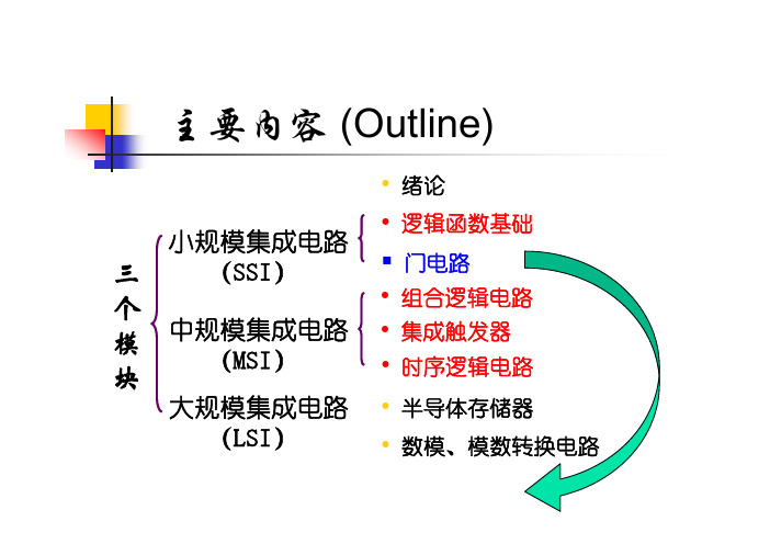
主要内容 (Outline)• 绪论小规模集成电路三(SSI)• 逻辑函数基础 门电路个• 组合逻辑电路模 块中规模集成电路 (MSI)• 集成触发器 • 时序逻辑电路大规模集成电路 • 半导体存储器(LSI)• 数模、模数转换电路绪论 (Introduction)一、数字(digital)信号和模拟(analog)信号 数字量和模拟量 数字电路和模拟电路二、数字信号相关概念 二进制数 Binary Digits 数字信号的逻辑电平 Logic Levels 数字信号波形 Digital Waveforms一、Digital Signal and Analog Signal Digital and Analog Quantities电子 电路 中的 信号模拟信号: 连续analogue signal value数字信号: 离散digital signal valuetime time模拟信号T( C) 30采样信号T( C)sampled3025离散化 2520202 4 6 8 10 12 2 4 6 8 10 12 t (h)A.M.P.M.2 4 6 8 10 12 2 4 6 8 10 12 t (h)A.M.P.M.数字化-表示 为由0、1组成 的二进制码Analog Electronic SystemDigital and Analog Electronic System★ 工作在模拟信号下的电子电路是模拟电路。
研究模拟电路时,注重电路输入、输出信号 间的大小、相位关系。
包括交直流放大器、 滤波器、信号发生器等。
★ 模拟电路中,晶体管一般工作在放大状态。
★ 工作在数字信号下的电子电路是数字电路。
研究数字电路时,注重电路输出、输入间的逻 辑关系。
主要的分析工具是逻辑代数,电路的 功能用真值表、逻辑表达式或波形图表示。
★ 在数字电路中,三极管工作在开关状态, 即工作在饱和状态或截止状态。
keb

optional: protection against restart/ power module switch off via ST
F5 - Multi /Servo
0,75 ... 355 kW
Closed loop inverter technology for synchronous and asynchronous motors
- FLAT REAR - Liquid-Cooled - Push through heat sink
or software solutions for applications like -LIFT -RBG/SRS -Serial Networking
KEB COMBIVERT F5 is a kit for a wide range of customized solutions in series business.
amplifier
Speed precontrol
Ramp generator ru.28 ru.1 ru.2 cs.0 = 1
AN1
Dig. Current set value
ru.27
% V
oP-Par.
cn.1
amplifier
Analog current set value
% V
AN2
cn.0 = 2
ru.29
ru.30 +
PID-controller ru.52
%
Hz
+
cs.4
+
An.-Par. cn.4...6 cn.10
cn.7...8
cnl value
ru.3 Frequency
cPCG包用户指南说明书
Package‘cPCG’October12,2022Type PackageTitle Efficient and Customized Preconditioned Conjugate GradientMethod for Solving System of Linear EquationsVersion1.0Date2018-12-30Author Yongwen ZhuangMaintainer Yongwen Zhuang<******************>Description Solves system of linear equations using(preconditioned)conjugate gradient algo-rithm,with improved efficiency using Armadillo templated'C++'linear algebra library,andflex-ibility for user-specified precondition-ing method.Please check<https:///styvon/cPCG>for latest updates.Depends R(>=3.0.0)License GPL(>=2)Imports Rcpp(>=0.12.19)LinkingTo Rcpp,RcppArmadilloRoxygenNote6.1.1Encoding UTF-8Suggests knitr,rmarkdownVignetteBuilder knitrNeedsCompilation yesRepository CRANDate/Publication2019-01-1117:00:10UTCR topics documented:cPCG-package (2)cgsolve (3)icc (4)pcgsolve (5)Index712cPCG-package cPCG-package Efficient and Customized Preconditioned Conjugate Gradient Methodfor Solving System of Linear EquationsDescriptionSolves system of linear equations using(preconditioned)conjugate gradient algorithm,with im-proved efficiency using Armadillo templated’C++’linear algebra library,andflexibility for user-specified preconditioning method.Please check<https:///styvon/cPCG>for latest up-dates.DetailsFunctions in this package serve the purpose of solving for x in Ax=b,where A is a symmetric andpositive definite matrix,b is a column vector.To improve scalability of conjugate gradient methods for larger matrices,the Armadillo templatedC++linear algebra library is used for the implementation.The package also providesflexibility tohave user-specified preconditioner options to cater for different optimization needs.The DESCRIPTIONfile:Package:cPCGType:PackageTitle:Efficient and Customized Preconditioned Conjugate Gradient Method for Solving System of Linear Equati Version: 1.0Date:2018-12-30Author:Yongwen ZhuangMaintainer:Yongwen Zhuang<******************>Description:Solves system of linear equations using(preconditioned)conjugate gradient algorithm,with improved effic Depends:R(>=3.0.0)License:GPL(>=2)Imports:Rcpp(>=0.12.19)LinkingTo:Rcpp,RcppArmadilloRoxygenNote: 6.1.1Encoding:UTF-8Suggests:knitr,rmarkdownVignetteBuilder:knitrIndex of help topics:cPCG-package Efficient and Customized PreconditionedConjugate Gradient Method for Solving System ofLinear Equationscgsolve Conjugate gradient methodicc Incomplete Cholesky Factorizationpcgsolve Preconditioned conjugate gradient methodcgsolve3Author(s)Yongwen ZhuangReferences[1]Reeves Fletcher and Colin M Reeves.“Function minimization by conjugate gradients”.In:Thecomputer journal7.2(1964),pp.149–154.[2]David S Kershaw.“The incomplete Cholesky—conjugate gradient method for the iter-ativesolution of systems of linear equations”.In:Journal of computational physics26.1(1978),pp.43–65.[3]Yousef Saad.Iterative methods for sparse linear systems.V ol.82.siam,2003.[4]David Young.“Iterative methods for solving partial difference equations of elliptic type”.In:Transactions of the American Mathematical Society76.1(1954),pp.92–111.Examples#generate test datatest_A<-matrix(c(4,1,1,3),ncol=2)test_b<-matrix(1:2,ncol=1)#conjugate gradient method solvercgsolve(test_A,test_b,1e-6,1000)#preconditioned conjugate gradient method solver,#with incomplete Cholesky factorization as preconditionerpcgsolve(test_A,test_b,"ICC")cgsolve Conjugate gradient methodDescriptionConjugate gradient method for solving system of linear equations Ax=b,where A is symmetric and positive definite,b is a column vector.Usagecgsolve(A,b,tol=1e-6,maxIter=1000)ArgumentsA matrix,symmetric and positive definite.b vector,with same dimension as number of rows of A.tol numeric,threshold for convergence,default is1e-6.maxIter numeric,maximum iteration,default is1000.4iccDetailsThe idea of conjugate gradient method is tofind a set of mutually conjugate directions for the unconstrained problemargmin x f(x)where f(x)=0.5b T Ab−bx+z and z is a constant.The problem is equivalent to solving Ax=b.This function implements an iterative procedure to reduce the number of matrix-vector multiplica-tions[1].The conjugate gradient method improves memory efficiency and computational complex-ity,especially when A is relatively sparse.ValueReturns a vector representing solution x.WarningUsers need to check that input matrix A is symmetric and positive definite before applying the function.References[1]Yousef Saad.Iterative methods for sparse linear systems.V ol.82.siam,2003.See AlsopcgsolveExamples##Not run:test_A<-matrix(c(4,1,1,3),ncol=2)test_b<-matrix(1:2,ncol=1)cgsolve(test_A,test_b,1e-6,1000)##End(Not run)icc Incomplete Cholesky FactorizationDescriptionIncomplete Cholesky factorization method to generate preconditioning matrix for conjugate gradi-ent method.Usageicc(A)ArgumentsA matrix,symmetric and positive definite.DetailsPerforms incomplete Cholesky factorization on the input matrix A,the output matrix is used for preconditioning in pcgsolve()if"ICC"is specified as the preconditioner.ValueReturns a matrix after incomplete Cholesky factorization.WarningUsers need to check that input matrix A is symmetric and positive definite before applying the function.See AlsopcgsolveExamples##Not run:test_A<-matrix(c(4,1,1,3),ncol=2)out<-icc(test_A)##End(Not run)pcgsolve Preconditioned conjugate gradient methodDescriptionPreconditioned conjugate gradient method for solving system of linear equations Ax=b,where A is symmetric and positive definite,b is a column vector.Usagepcgsolve(A,b,preconditioner="Jacobi",tol=1e-6,maxIter=1000) ArgumentsA matrix,symmetric and positive definite.b vector,with same dimension as number of rows of A.preconditioner string,method for preconditioning:"Jacobi"(default),"SSOR",or"ICC".tol numeric,threshold for convergence,default is1e-6.maxIter numeric,maximum iteration,default is1000.DetailsWhen the condition number for A is large,the conjugate gradient(CG)method may fail to converge in a reasonable number of iterations.The Preconditioned Conjugate Gradient(PCG)Method appliesa precondition matrix C and approaches the problem by solving:C−1Ax=C−1bwhere the symmetric and positive-definite matrix C approximates A and C−1A improves the con-dition number of A.Common choices for the preconditioner include:Jacobi preconditioning,symmetric successive over-relaxation(SSOR),and incomplete Cholesky factorization[2].ValueReturns a vector representing solution x.PreconditionersJacobi:The Jacobi preconditioner is the diagonal of the matrix A,with an assumption that all diagonal elements are non-zero.SSOR:The symmetric successive over-relaxation preconditioner,implemented as M=(D+L)D−1(D+ L)T.[1]ICC:The incomplete Cholesky factorization preconditioner.[2]WarningUsers need to check that input matrix A is symmetric and positive definite before applying the function.References[1]David Young.“Iterative methods for solving partial difference equations of elliptic type”.In:Transactions of the American Mathematical Society76.1(1954),pp.92–111.[2]David S Kershaw.“The incomplete Cholesky—conjugate gradient method for the iter-ativesolution of systems of linear equations”.In:Journal of computational physics26.1(1978),pp.43–65.See AlsocgsolveExamples##Not run:test_A<-matrix(c(4,1,1,3),ncol=2)test_b<-matrix(1:2,ncol=1)pcgsolve(test_A,test_b,"ICC")##End(Not run)Index∗methodscgsolve,3icc,4pcgsolve,5∗optimizecgsolve,3pcgsolve,5∗packagecPCG-package,2cgsolve,3,6cPCG(cPCG-package),2cPCG-package,2icc,4pcgsolve,4,5,5preconditioner(pcgsolve),57。
HP M42381-001 用户指南说明书

User Guide *M42381-001*M42381-001RMN: HSN-PD02© Copyright 2020 HP Development Company, L.P.All rights reserved. Android is a trademark of Google LLC. Linux® is the registered trademark of Linus Torvalds in the U.S. and other countries. Microsoft and Windows are either registered trademarks or trademarks of Microsoft Corporation in the United States and/or other countries. Enterprise Linux and Red Hat are trademarks of Red Hat, Inc. in the United States and other countries.The information contained herein is subject to change without notice. The only warranties for HP products and services are set forth in the express warranty statements accompanying such products and services. Nothing herein should be construed as constituting an additional warranty. HP shall not be liable for technical or editorial errors or omissions contained herein.First Edition: October 2020Document Part Number: M42381-001Product noticeThis user guide describes features that are common to most models. Some features may not be available on your computer.To access the latest user guides, go to /support, and follow the instructions to find your product. Then select Manuals.Software termsBy installing, copying, downloading, or otherwise using any software product preinstalled on this computer, you agree to be bound by the terms of the HP End User License Agreement (EULA). If you do not accept these license terms, your sole remedy is to return the entire unused product (hardware and software) within 14 days for a full refund subject to the refund policy of your seller.For any further information or to request a full refund of the price of the computer, please contact your seller.Contents1.Introduction (4)e and disclosure (4)2.Specification (5)2.1.General specification (5)2.2.Electrical specification (6)2.2.1.Block diagram (6)2.2.2.Power request (6)munication interface (6)2.2.4.Mechanical drawing (7)3.Software (8)3.1.Supported operating systems (8)mand list (9)3.2.1.ULTIMATE command mode (9)4.Appendix (11)4.1.Table 1 Codepage list (11)4.2.Table 2 International character set (11)1.Introductione and disclosureThis document shall apply only to the product(s) identified herein. This technical specification defines the requirements for HP Engage 3x16 Pole Display, using a USB bus power interface.The supplier is requested to implement a change control process for tracking all changes, including revision history. Devices shall be labeled and identifiable based on the revision. After the release to production, all changes must be communicated as an Engineering Change.2.Specification2.1.General specificationItem HSN-PD02Display Method Vacuum Fluorescent Display (Blue-green) Resolution 256 × 64 DotsDisplay Mode Alphanumeric: 32 digits × 3 lines 32 digits × 4 linesCharacter Dot Matrix 8 × 16 dots for single-byte characters 16 × 16 dots for double-bytes charactersDot Size 0.49 (W) × 0.48 (H) mmDot Pitch 0.64 (H) × 0.63 (V) mmViewing Direction Maximum 90°Average Brightness 600 cd/m2Character type Alphanumeric and Compound (2-Bytes) WordsCharacter size Font 8 × 16 – 4.97 (W) × 9.93 (H) mm Font 16 × 16 – 10.09 (W) × 9.93 (H)mmUser Define Character 96 charactersViewing Area 163.69(W)X40.17 (H) mm Module Dimension 230 (L) × 66.5 (W) × 26 (D) mm Top Head Dimension 240 (L) × 95 (W) × 49 (D) mm Viewing Angle Maximum 90°Net Weight Approximately 1650 grams Commands Mode UITIMATELanguage US English, JapaneseInterface USBBaud rate Direct connection 9600 or 19200 bps MTBF 30,000 hoursPower Consumption 12 V – 400 mAEMC / Safety standards CB, VCCI2.2. Electrical specification2.2.1. Block diagram2.2.2. Power requestVoltage (typical): 12 VDC +/- 10%Current consumption (typical): 400 mA2.2.3. Communication interfaceInterface USB (Virtual COM Port) The default protocol of the virtual RS232 port is 9600 bps, non-parity, 8 data bits, 1 stop bit and with DTR/DSR control.VFDMCUUSB UART Control & DataPowerUSB INPUTDC INPUT EEPROM2.2.4.Mechanical drawing3.Software3.1.Supported operating systemsWindows●Windows® 10●Windows 8.1/8 Pro (64 and 32 bit)●Windows Embedded 8.1/8 Industry●Windows Embedded POSReady 7 (64 and 32 bit)●Windows 7 Professional (64 and 32 bit)●Windows Embedded POSReady 2009Linux●Red Hat® Enterprise Linux®/CentOS 6 (64 and 32 bit) and newer●Suse Linux® Enterprise Point of Service 11 (64 or 32 bit) and newer●Ubuntu 12.04 LTS (64 or 32 bit) and newerAndroid●Android™ 4.0 and newermand list3.2.1.ULTIMATE command modeCommand Hex Function DescriptionHT 09 Move cursor rightBS 08 Move cursor leftUS LF 1F 0A Move cursor upLF 0A Move cursor downUS CR 1F 0D Move cursor to right-most positionCR 0D Move cursor to left-most positionHOM 0B Move cursor to home positionUS B 1F 42 Move cursor to bottom positionUS $ x y1F 24 x y Move cursor to specified position1≦x(column)≦20 ; 1≦y(row)≦2US C n1F 43 n Select/cancel cursor displayn=0, canceled ; n=1, selectedCLR 0C Clear display screenCAN 18 Clear cursor lineUS X n1F 58 n Brightness adjustment1 ≦n≦ 4US E n1F 45 n Blink display screen0≦n≦255 (n*50msec) ON / (n*50msec) OFFn=0, blinking is canceledn=255, display is turned offESC @ 1B 40 Initialize displayESC t n1B 74 n Select character code table (see Table 1) ESC R n1B 52 n Select international character set (see Table 2) US r n1F 72 n Select/cancel reverse charactern=0, canceled; n=1, selectedUS MD1 1F 01 Specify overwrite modeUS MD2 1F 02 Specify vertical scroll modeUS MD3 1F 03 Specify horizontal scroll modeUS T h m1F 54 h m Set and display time0≦h≦23 ; 0≦m≦59US U 1F 55 Display of time counterESC u E..CR 1B 75 45 hh 3A mm 0D Set and display 24-hour time0x30≦h ,m≦0x39ESC u 1..CR 1B 75 49 [data x 40] 0D Two-line displayESC [ D 1B 5B 44 Move cursor leftESC [ C 1B 5B 43 Move cursor rightESC [ A 1B 5B 41 Move cursor upESC [ B 1B 5B 42 Move cursor downESC [ H 1B 5B 48 Move cursor to home position ESC [ L 1B 5B 4C Move cursor to left-most position ESC [ R 1B 5B 52 Move cursor to right-most position ESC [ K 1B 5B 4B Move cursor to bottom position ESC l x y1B 6C x y Move cursor to specified position1≦x≦20, y=1,2ESC u A..CR 1B 75 41 [data x 32] 0D Display data on line 1ESC u B..CR 1B 75 42 [data x 32] 0D Display data on line 2ESC u C..CR 1B 75 43 [data x 32] 0D Display data on line 3GS r A1D 72 41 [data x 96] 0D Marquee on line 1GS r B1D 72 42 [data x 96] 0D Marquee on line 2GS r C1D 72 43 [data x 96] 0D Marquee on line 3GS r D1D 72 44 [data x 96] 0D Marquee on line 44.Appendix4.1.Table 1 Codepage listPageCodepage Language Dec Hex0 0x00 PC437 USA, Standard Europe1 0x01 Katakana Japanese244 0xF4 CP932 Japanese Shift JIS 4.2.Table 2 International character setIndex nCountry ASCII codeDec Hex 23 24 40 5B 5C 5D 5E 60 7B 7C 7D 7E00 00 USA # $ @ [ \ ] ^ ` { | } ~01 01 France # $ à ° ç § ^ ` é ù è ¨02 02 Germany # $ § Ä Ö Ü ^ ` ä ö ü β03 03 U.K. £ $ @ [ \ ] ^ ` { | } ~04 04 Denmark I # $ @ Æ Ø Å ^ ` æ ø å ~05 05 Sweden # ¤É Ä Ö Å Ü é ä ö å ü06 06 Italy # $ @ ° \ é ^ ù à ò è ì07 07 Spain I Pt $ @ ¡ Ñ ¿ ^ ` ¨ ñ } ~08 08 Japan # $ @ [ ¥ ] ^ ` { | } ~09 09 Norway # ¤É Æ Ø Å Ü é æ ø å ü10 0A Denmark II # $ É Æ Ø Å Ü é æ ø å ü11 0B Spain II # $ á ¡ Ñ ¿ é ` í ñ ó ú12 0C Latin America # $ á ¡ Ñ ¿ é ü í ñ ó ú13 0D Korea # $ @ [ ₩] ^ ` { | } ~14 0E Slovenia/Croatia # $ ŽŠ ĐĆČžš đćč15 0F China # Ұ@ [ \ ] ^ ` { | } ~16 10 Vietnam ₫$ @ [ \ ] ^ ` { | } ~17 11 Slovakia # $ @ [ \ ] ^ ` { | } ~18 12 Russia # $ @ [ \ ] ^ ` { | } ~。
各种常用统计分布之间的逻辑框架图

Relationships Among Common Univariate DistributionsAuthor(s): Lawrence M. LeemisSource: The American Statistician, Vol. 40, No. 2 (May, 1986), pp. 143-146Published by: American Statistical AssociationStable URL: /stable/2684876Accessed: 25/01/2010 08:15Your use of the JSTOR archive indicates your acceptance of JSTOR's Terms and Conditions of Use, available at/page/info/about/policies/terms.jsp. JSTOR's Terms and Conditions of Use provides, in part, that unless you have obtained prior permission, you may not download an entire issue of a journal or multiple copies of articles, and you may use content in the JSTOR archive only for your personal, non-commercial use.Please contact the publisher regarding any further use of this work. Publisher contact information may be obtained at/action/showPublisher?publisherCode=astata.Each copy of any part of a JSTOR transmission must contain the same copyright notice that appears on the screen or printed page of such transmission.JSTOR is a not-for-profit service that helps scholars, researchers, and students discover, use, and build upon a wide range of content in a trusted digital archive. We use information technology and tools to increase productivity and facilitate new forms of scholarship. For more information about JSTOR, please contact support@.American Statistical Association is collaborating with JSTOR to digitize, preserve and extend access to TheAmerican Statistician.。
M-503(Cathodic protection)

5 5 5 6 7 7 7 7 8
8 8 8 9 9 10
10
10 10 11
12
NORSOK standard
Page 1 of 12
NORSOK standard M-503
Edition 3, May 2007
Foreword
The NORSOK standards are developed by the Norwegian petroleum industry to ensure adequate safety, value adding and cost effectiveness for petroleum industry developments and operations. Furthermore, NORSOK standards are, as far as possible, intended to replace oil company specifications and serve as references in the authorities’ regulations.
The NORSOK standards are prepared and published with support by The Norwegian Oil Industry Association (OLF), The Federation of Norwegian Industry, Norwegian Shipowners’ Association and The Petroleum Safety Authority Norway.
3 3.1 3.2
Terms, definitions, abbreviations and symbols Terms and definitions Abbreviations and symbols
TCP_Persistence_Techniques

11
ILM and TCP Freeze Option
APP
APP
Indirect Layer
16
Link Detection
DHCP: Change of IP address or network prefix TCP Keep-alive mechanism ICMP heartbeat probe mechanism which the out-band UDP signaling is used to constantly probe the disconnection/ service inactivity Trade-off (frequency/ traffic)
4
Goals
Users manually states the requirement of having continuous connection for their applications regardless of user movement and link disconnection.
Unexpected disconnection
Roaming (Handoff issue: Change of IP) Long period of link disconnection Server down
Expected disconnection
Laptop Hibernation
Policy based control
经典六西格玛(6sigma)培训内部资料M_02_Capa.
M 02-1M 02-2M 02-3M 02-4M 02-5M 02-6M 02-7M 02-8M 02-9M 02-10Qualitative Y (attribute data Y的定性分析(计数型数据) Capability determination for an attribute output: Qualitative Y (attribute data Y的定性分析(计数型数据)对计数型输出的能力确定: Tally Defect Data 缺陷数据确认 Compute PPM 计算PPM Step 2(步骤2: » Compute the proportion of defects and the PPM 计算缺陷的比例和PPM Step 1: » Verify the definition / description of a defect 验证缺陷的定义/描述 » Count the occurrence of defects (and track the total units processed. Historical data is typically used here and usually considered to be longterm. 步骤1: 计算缺陷数量(并计算总产量。
通常可以使用历史数据并当作长期来考虑。
62 Step3(步骤3: 4 Compute the Z-score and shift by 1.5 if appropriate 计算Z值,适用时偏移1.5 Compute Z-score 计算Z值 Step 4(步骤4: 5 Estimate traditional capability indices 估计能力指标 » Change from Z to Cp, Cpk, Pp, Ppk 将Z转化成Cp, Cpk, Pp, Ppk Introduction to Six Sigma Compute Cpk, Ppk 计算Cpk, Ppk Introduction to Six Sigma 61 Qualitative Y (attribute data Y的定性分析(计数型数据) ParetoC by P hart roduct Tally Defect Data 缺陷数据确认 Scrapped Units 100 6000 5000 4000 3000 2000 1000 0 20 0 80 60 40 Calculate PPM 计算PPM Calculate Z-score 计算Z值 Calculate Cpk, Ppk 计算Cpk, Ppk Exercise: Using the Pareto chart given below, calculate the capability of the Intrepid product to be shipped defect free: 练习:用下面的Pareto图,计算 Intrepid 交付无缺陷产品的能力 id rt s rs rep Isuzu sco Lexu the E O Int Total Units: 35000 5000 60000 15000 20000 Introduction to Six Sigma 64 Introduction to Six Sigma 63 Steps 1 :Tally Defect Data 步骤1:缺陷数据计数 Steps 2 :Calculate PPM 步骤2:计算PPM Step 2(步骤2: ParetoC by Product hart 100 6000 Step 1(步骤1: Scrapped Units Assume:Opportunity equals 1 per unit 假设:每个产品有一个缺陷机会 Intrepid defect count: 4000 Intrepid total units produced: 35000 Intrepid产品缺陷数量:4000 Intrepid产品总产量:35000 Percent Verify the definition / description of a defect. 验证缺陷的定义/描述。
1绪论理想气体

返回
• 物理化学是化学领域一门非常重要和关键的基 础学科。它在化学、材料、化工、生物、医药 等领域有着广泛的应用。 • 定义:应用物理学原理和方法研究有关化学现 象和化学过程的一门科学。 • 物理化学主要是为了解决生产实际和科学实验 中向化学提出的理论问题,揭示化学变化的本 质,更好地驾驭化学,使之为生产实际服务。
用量子力学的基本方程(E.Schrodinger方程)求 解组成体系的微观粒子之间的相互作用及其规律,从 而指示物性与结构之间的关系。
上一内容 下一内容 回主目录
返回
三、物理化学的研究内容
①化学热力学——化学变化的方向和限度,以及伴随发生的 能量转换关系; 例如合成氨,常温常压下能否进行?产率? ②化学动力学——化学反应的速率和机理; 上例理论上可行。关键是寻找合适的催化剂和反应途径( 模拟生物固氮) ③结构化学——物质的性质与其微观结构的关系 例如研究与氮分子有关的配合物的结构,以及它们在不同 条件下的变化,就有利于常温常压下寻找固氮的途径。
其物理意义:p是一个状态函数,dp只与始、终 态有关,而与途径无关。
⒋全微分的性质:
p p V T V T T V T V
上一内容
下一内容
回主目录
返回
⒌微分法则与积分法则(查数学手册)
Chapter 1 Gas
• 本章基本要求: • 掌握理想气体状态方程 • 掌握理想气体的宏观定义及微观模型 • 掌握分压、分体积概念及计算。 • 理解真实气体与理想气体的偏差、临界现象。 • 掌握饱和蒸气压概念 • 理解范德华状态方程、对应状态原理和压缩因子图,了解 对比状态方程及其它真实气体方程。
德文)。 二十世纪迅速发展:新测试手段和新的数据处理方法不断涌现,形成 了许多新的分支学科,如:热化学,化学热力学,电化学,溶液化学 ,胶体化学,表面化学,化学动力学,催化作用,量子化学和结构化 学等。
Sierra Wireless AirPrime XA1100 XM1100 EVK用户手册说明书

AirPrime XA1100/XM110041111189Rev 1AirPrime XA1100/XM1100 EVK User GuideImportant Notice Due to the nature of wireless communications, transmission and reception of data can never be guaranteed. Data may be delayed, corrupted (i.e., have errors) or be totally lost. Although significant delays or losses of data are rare when wireless devices such as the Sierra Wireless modem are used in a normal manner with a well-constructed network, the Sierra Wireless modem should not be used in situations where failure to transmit or receive data could result in damage of any kind to the user or any other party, including but not limited to personal injury, death, or loss of property. Sierra Wireless accepts no responsibility for damages of any kind resulting from delays or errors in data transmitted or received using the Sierra Wireless modem, or for failure of the Sierra Wireless modem to transmit or receive such data.Safety and Hazards Do not operate the Sierra Wireless modem in areas where blasting is in progress, where explosive atmospheres may be present, near medical equipment, near life support equipment, or any equipment which may be susceptible to any form of radio interference. In such areas, the Sierra Wireless modem MUST BE POWERED OFF. The Sierra Wireless modem can transmit signals that could interfere with this equipment.Do not operate the Sierra Wireless modem in any aircraft, whether the aircraft is on the ground or in flight. In aircraft, the Sierra Wireless modem MUST BE POWERED OFF. When operating, the Sierra Wireless modem can transmit signals that could interfere with various onboard systems.Note:Some airlines may permit the use of cellular phones while the aircraft is on the ground and the door is open. Sierra Wireless modems may be used at this time.The driver or operator of any vehicle should not operate the Sierra Wireless modem while in control of a vehicle. Doing so will detract from the driver or operator's control and operation of that vehicle. In some states and provinces, operating such communications devices while in control of a vehicle is an offence.Limitation of Liability The information in this manual is subject to change without notice and does not represent a commitment on the part of Sierra Wireless. SIERRA WIRELESS AND ITS AFFILIATES SPECIFICALLY DISCLAIM LIABILITY FOR ANY AND ALL DIRECT, INDIRECT, SPECIAL, GENERAL, INCIDENTAL, CONSEQUENTIAL, PUNITIVE OR EXEMPLARY DAMAGES INCLUDING, BUT NOT LIMITED TO, LOSS OF PROFITS OR REVENUE OR ANTICIPATED PROFITS OR REVENUE ARISING OUT OF THE USE OR INABILITY TO USE ANY SIERRA WIRELESS PRODUCT, EVEN IF SIERRA WIRELESS AND/OR ITS AFFILIATES HAS BEEN ADVISED OF THE POSSIBILITY OF SUCH DAMAGES OR THEY ARE FORESEEABLE OR FOR CLAIMS BY ANY THIRD PARTY.Notwithstanding the foregoing, in no event shall Sierra Wireless and/or its affiliates aggregate liability arising under or in connection with the Sierra Wireless product, regardless of the number of events, occurrences, or claims giving rise to liability, be in excess of the price paid by the purchaser for the Sierra Wireless product.Preface Patents This product may contain technology developed by or for Sierra Wireless Inc. Thisproduct includes technology licensed from QUALCOMM®. This product ismanufactured or sold by Sierra Wireless Inc. or its affiliates under one or morepatents licensed from InterDigital Group and MMP Portfolio Licensing. Copyright© 2017 Sierra Wireless. All rights reserved.Trademarks Sierra Wireless®, AirPrime®, AirLink®, AirVantage® and the Sierra Wireless logoare registered trademarks of Sierra Wireless.Windows® and Windows Vista® are registered trademarks of MicrosoftCorporation.Macintosh® and Mac OS X® are registered trademarks of Apple Inc., registered inthe U.S. and other countries.QUALCOMM® is a registered trademark of QUALCOMM Incorporated. Usedunder license.Other trademarks are the property of their respective owners.ContactInformation Revision History Sales information and technicalsupport, including warranty and returnsWeb: /company/contact-us/Global toll-free number: 1-877-687-77956:00 am to 6:00 pm PSTCorporate and product information Web: RevisionnumberRelease date Changes1June 23, 2017Initial revision in SWI TemplateContentsIntroduction . . . . . . . . . . . . . . . . . . . . . . . . . . . . . . . . . . . . . . . . . . . . . . . . . . . . .5 Caution. . . . . . . . . . . . . . . . . . . . . . . . . . . . . . . . . . . . . . . . . . . . . . . . . . . . . . 6 Packing Contents. . . . . . . . . . . . . . . . . . . . . . . . . . . . . . . . . . . . . . . . . . . . . . 6Function Description . . . . . . . . . . . . . . . . . . . . . . . . . . . . . . . . . . . . . . . . . . . . .7Function Testing . . . . . . . . . . . . . . . . . . . . . . . . . . . . . . . . . . . . . . . . . . . . . . . .10 Preparation for Power and Data Communication (XA1100, XM1100 not using 3D-Fix function) . . . . . . . . . . . . . . . . . . . . . . . . . . . . . . . . . . . . . . . . . . . . . . 10 Application for the various RF reception. . . . . . . . . . . . . . . . . . . . . . . . . . . . 11Software Usage . . . . . . . . . . . . . . . . . . . . . . . . . . . . . . . . . . . . . . . . . . . . . . . . .12 System Requirements . . . . . . . . . . . . . . . . . . . . . . . . . . . . . . . . . . . . . . . . . 12 USB Driver and GNSS Tool. . . . . . . . . . . . . . . . . . . . . . . . . . . . . . . . . . . . . 12 Installing the USB Driver . . . . . . . . . . . . . . . . . . . . . . . . . . . . . . . . . . . . . . . 12 Using GNSS Tool. . . . . . . . . . . . . . . . . . . . . . . . . . . . . . . . . . . . . . . . . . . . . 14RTCM Hardware Settings . . . . . . . . . . . . . . . . . . . . . . . . . . . . . . . . . . . . . . . . .16 Getting RTCM data via RS232port . . . . . . . . . . . . . . . . . . . . . . . . . . . . .16RTCM Software Settings . . . . . . . . . . . . . . . . . . . . . . . . . . . . . . . . . . . . . . . . .17Troubleshooting . . . . . . . . . . . . . . . . . . . . . . . . . . . . . . . . . . . . . . . . . . . . . . . .19 Setup Troubleshooting. . . . . . . . . . . . . . . . . . . . . . . . . . . . . . . . . . . . . . . . . 19 Causes of Poor GPS Signals. . . . . . . . . . . . . . . . . . . . . . . . . . . . . . . . . . . . 201 1: IntroductionThe main purpose of this EV-Kit is to simplify the evaluation process for GPS modulesand to help testers operate our products with convenience and ease.This device can communicate with computer devices via USB, and must be used inconjunction with the GNSS Tool software application. You can record all GPS moduledata such as satellites’ status, time-to-first-fix (TTFF), date and time.If you evaluate the RTCM function, it will show you how to run the GNSS Tool with theEV-Kit via RS232 (DB-9 Connector).The EV-Kit was divided into two series, basing on the various modules listed below.Left: With External Antenna (series 1). Right: Built-in Switch Antenna input (series 2).Figure 1-1:Left: Iovry 2. Right: XA1100Figure 1-2:XM1100AirPrime XA1100/XM1100 EVK User GuideCaution•Global position system (GPS) is the property of American Ministry of NationalDefense; they are fully responsible for the preciseness and maintenance ofthe system. Any changes they have implemented to the system in the futuremay enhance or deteriorate the effectiveness and performance of thereceived GPS data.•The GPS signal might be cut-off or become seriously weakened if youoperate the EV-kit inside any infrastructures such as buildings, tunnels, ornearby any huge objects and/or obstructions. The kit has not malfunctionedand will operate properly again once it receives clear GPS signals (worksbest under open sky).•To avoid damaging the intricate electronic components and circuitry, pleasedo not place the EV-Kit directly under the sun for long periods of time.Packing Contents•User Manual / Software Application Program•CP210X USB Bridge VCP driver•GNSS Tool with user manual•EV-Kit user manualNote:These items will be delivered by E-mail. Please contact your dealer for the items formore information.•USB Cable•EV-Kit with Main Board and GPS Module•External Antenna2 2: Function DescriptionThe following figures illustrate and describe the EV-Kit device:Figure 2-1:Compatible Models (Series 1): Iovry 2AirPrime XA1100/XM1100 EVK User GuideFigure 2-2:Compatible Models (Series 1): XM1100Function DescriptionFigure 2-3:Compatible Models (Series 2): XA11003 3: Function TestingPreparation for Power and DataCommunication (XA1100, XM1100 not using3D-Fix function)1.Connect the USB cable with the PC.·The EV-Kit will turn on with USB power and the EV-Kit will transfer communi-cation data with the PC.·Make sure Power LED Indicator (D1) light is lighted on.2.Turn on the power for the GPS module:The switch enables the LDO to supply power for the GPS Module. Please refer tothe figures shown below.a.Once the Power LED Indicator(D1) is on and main board enable switch(SW1)is on, the initial state will be the following:3D Fix LED Indicator (D2) blinks (blue light).1PPS LED Indicator (D3) is off (green light).b.Once the module is in the status of FIX:3D Fix LED Indicator (D2) is off.1PPS LED Indicator (D3) green is blinking.Figure 3-1:ComponentsFunction TestingApplication for the various RF reception e an External Antenna with the GPS Module as shown in Figure3-2.Compatible Model (series1): Ivory 2, XM1110.Figure 3-2:Using an External Antenna2.Connect an External Antenna with the GPS Module as shown in Figure3-3.Compatible Model (series 2): XA1100.Figure 3-3:Using an External AntennaAs soon as you connect an external antenna, the internal RF switch will wire the RF signal from external antenna. If the external antenna is removed, it will auto-switch to the built-in patch antenna.Note:the module will detect and connect to the external antenna when it begins to consume >4mA current.4 4: Software UsageSystem Requirements•Operation System: Windows OS 7, 8, and 10•USB Driver: CP210x VCPInstaller.zip•GUI Tool: GNSS Tool·Microsoft .NET Framework 4.5·Microsoft Visual C++ 2015 Redistributable Package (x86)USB Driver and GNSS ToolBefore setting up the connection between the module and the PC, please downloadand install the VCP driver from the following link.From Silicon Labs Web-side (CP210x USB to UART Bridge VCP Drivers):/products/mcu/Pages/USBtoUARTBridgeVCPDrivers.aspxYou will need the EV-Kit USB Driver (CP210xVCP) and GNSS Tool.exe to operate theEV-Kit.Important:Please check whether you have the correct USB driver before you proceed to thenext step. Without the correct driver, the EV-Kit will not function.Installing the USB Driver1.Double click CP210x_VCP_Win.exe to begin driver installation:Figure 4-1:Driver Installation Folder2.Click Install:Software UsageFigure 4-2:Starting the Installation Process3.After the installation is complete, you may need to restart your computer.Please follow the instructions on screen to restart your computer.4.After the computer restarted, right click on My Computer and selectManage:Figure 4-3:Selecting Manage5.Left click Device Manager and select Ports (COM &LPT). Check to see if adevice named Silicon Labs CP210x USB to UART Bridge (COM#) ispresent. If so, the EV-Kit is set up and ready for use.AirPrime XA1100/XM1100 EVK User GuideFigure 4-4:Accessing the Port Properties“COM9” in this example represents the virtual COM port number generated forthe USB connection to the EV-Kit. This generated COM port value must matchthe COM port value in the program setting for the application to establish propercommunication with the EV-Kit.After completing the installation, please proceed to Using GNSS Tool.Using GNSS ToolMicrosoft Framework 4.5 or higher is required before you launch the GNSS Toolsoftware on your PC.Double click GNSSTool.exe to start the application, the main screen of theprogram is shown here:Figure 4-5:GNSSTool main screenSoftware Usage mand Tx and Rx List: clicking on this menu item will display theCommand window.2.NMEA List: clicking on this menu item will display a window with NMEA infor-mation.R Signal: clicking on this menu item will display the CNR signal window.4.Sky View: clicking on this menu item will display a window with a sky view ofsatellites.5.Statistics Plot: clicking on this menu item will display the statistics plotwindow.6.Map: clicking on this menu item will display the map window.After the Sierra Wireless EV-Kit is connected with the PC, please choose the correct <COM Port> and < Baud Rate > then click the OK button and select the appropriate value.When users click the Open Communication menu item or toolbar button, a set up dialog will pop up as shown here:Figure 4-6:COM Port DialogIf you want more information about the GNSS Tool software, refer to the Sierra Wireless GNSS Tool Operation Manual.Compatible Models: Iovry 2Getting RTCM data via RS232portConnect the RS232 cable to the EV-Kit. The RS232 cable is connected to the EV-Kit RS232 port (J2) and to the RTCM server (host computer) as shown below:Figure 5-1:RS232 ConnectionThe Ntrip client function can connect to the specified Ntrip caster and create the RTCM streaming. Before connecting to an Ntrip caster, please set up the required parameters properly.Clicking the drop down arrow show the Settings menu:Figure 6-1:Settings MenuAfter clicking the Settings menu, the Ntrip Client Settings dialog pop up as appears as shown below:Figure 6-2:NTrip Client Settings7.Choose a proper stream which meets yours RTCM version.8.Input the address and port numbers of the specified caster and the authorizedusername and password to log in.9.Designate a fixed location by inputting the latitude and longitude. This referencelocation information will be sent to the Ntrip caster to get more accurate RTCM correction data.10.Choose the specified serial port and baud rate.AirPrime XA1100/XM1100 EVK User GuideAfter the set up is complete click the RTCM button to enable the RTCM functionas shown here:Figure 6-3:Clicking the RTCM button to enable the RTCM function.77: Troubleshooting Setup TroubleshootingNote:if these troubleshooting steps do not solve the problem, please contact us or send it back to us for testing and repair.Table 7-1:Troubleshooting Causes and Solutions Problem Possible Cause SolutionCannot find GPS device USB was not set up properly Check to see if the EV-Kit was set up properly, and make sure that thedevice is receiving enough powerthrough the USB cable (Red LEDshould light up continuously).No NMEA data or GPS signals B was not set up Port or Baud rate value is incorrect. 1.Check to see if the USB connector to the PC or EV-Kit is tightlyconnected.2.Double check to see if the properCOM Port and Baud rate valueare selected.Poor GPS Signal Reception 1.If it is used inside a vehicle, the anti-sunscreen film on the windshield may interfere and weaken the GPSsignal.2.The vehicle istraveling through anarea with a denseoverhead canopy:such as forest,buildings, opentunnels etc.For both problems, the user may apply the External Active Antenna with theEV-Kit, and then place the antenna ontop of the car’s roof to improve signalreception.AirPrime XA1100/XM1100 EVK User GuideCauses of Poor GPS SignalsIt is possible to have weak GPS signal in the following situations:Table 7-2:Examples where Poor GPS Signals may OccurInside a tunnel, where the GPS signal is blocked.Underneath infrastructure (e.g. bridge), where the GPS signal isblocked.Inside a building, where the GPS signal is blocked.TroubleshootingRev 1 Jun.172141111189•If the EV-Kit is used inside a car which has anti-sunlight films on the windshield and windows, the GPS signal will be weakened severely, and may result in no GPS reception.•GPS satellites are property of United States Army. Sometimes they will tune-down the accuracy for unknown reasons. In such cases, the GPS position may not be accurate.Next to tall buildings, where the GPS signal is weakened.Underneath forests or any other kinds of canopy where GPSsignal is weakened.Table 7-2:Examples where Poor GPS Signals may Occur。
IBM-PC AT兼容计算机与PLC-5系列处理器之间的连接接口说明书

1AllenĆBradley Peer Communication Link Interface Module(Cat. No. 1784-KTK1)Product Data The 1784-KTK1 is a part of the 1784-PT5 Programming TerminalInterface package which contains the components necessary to completethe link between your IBM-PC/AT compatible computer and any PLC-5family processor. The Allen-Bradley Company supplies the 1784-PT5Programming Terminal Interface Package with with the followingcomponents:1784-KTK1 Peer Communication Link Interface Module1784-CP5 Communication Cable to PLC-5 processor6201-DDA PLC-5 Programming Software for IBM-AT compatiblecomputers (5-1/4 inch floppy disk) and the PLC-5 ProgrammingSoftware User’s Manual1784ĆPT5 Ordering Information2CompatiblesAllen-Bradley has verified the 6201-DDA software in the followingIBM-AT compatibles:IBM-ATAT&T 6300Compaq Portable 286Compaq Portable IINote: The 1784-T50 Industrial Terminal comes with the required6226-DDB PLC-5 Industrial Terminal Support Software (3-1/2 inch floppy disk) and associated documentation.The Peer Communication Link (PCL) Interface Module allows anAllen-Bradley 1784-T50 terminal or an IBM-AT compatible computer to communicate directly with a single PLC-5 family controller or, if connected to a Peer Communication Link, to all controllers and terminals on the PCL.The 1784-KTK1 board can reside in any available 16-bit slot of the1784-T50 or an IBM-PC/AT compatible; it physically requires two slots.Single-cable connection to PLC-5Slot addressable, may be used with other option boards installed in your computerLadder element intensificationRequires no external powerOn-line programmingUpload/download capabilityOn-line data monitorData changeProcessor mode changeI/O forcingTest-edit modeIntroduction and General DescriptionFeatures and Benefits3The 1784-PT5 package provides 1784-T50 Industrial Terminal emulationcapabilities to users of IBM-AT compatible computers. The included6201-DDA software duplicates the on-line functions available on the T50Industrial Terminal. The 1784-KTK1 PCL Communication Interfacemodule is installed in your computer to support the “handshaking” routinesnecessary for your computer and PLC-5 processor(s) to communicate witheach other.Connection from the 1784-KTK1 module to the Peer Communication Linkrequires only one cable that plugs directly in to a PLC-5 family processor.From this one connection you are linked to all other PLC-5’s on the PCL(Figure 1).Operation4Figure 11784ĆKTK1 Interface Module Placement on a PCLMenu screens provided by the 6201-DDA software (IBM-AT compatibles) or 6226-DDB software (1784-T50 Industrial Terminals) direct you through communication and addressing setups.5Note: The use of other boards along with the 1784-KTK1 may result in expansion slot bus address conflicts. We suggest resetting the 1784-KTK1to one of the noted addresses in Table 1.You can install this module in any Allen-Bradley T50 Industrial Terminalor IBM-AT compatible computer; however, certain handling precautionsmust be observed to prevent damage to the board during installation.Electrostatic DischargeElectrostatic discharge can degrade performance or damage the module. Ifyou observe the following precautions you can guard against electrostatic damage.Touch a grounded object to rid yourself of charge before handling the module.Do not touch the backplane connector or connector pins.If you set configuration plugs or switches or replace internalcomponents, do not touch other circuit components inside the module. If available, use a static-safe work station.When not in use, keep the module in its static-shield bag.Installation ProceduresTo install the 1784-KTK1 board into your T50 Industrial Terminal ,follow the instructions in the Industrial Terminal User’s Manual (Pub. No.1784-6.5.1).Software installation instructions are in the PLC-5Programming Software User’s manual (Pub. No. 6226-6.5.1)To install the 1784-KTK1 board into your IBM-PC/AT compatiblecomputer:1.Turn the computer off and remove the ac line cord.2.Next, verify that two adjacent backplane slots are available. TheKTK1 PCL board requires only one slot for its connections, but it istwo slots wide.3.At the desired slot location remove the screw holding theoption-retaining bracket and remove the bracket.4.Determine what memory address the board should have and set theswitchpack on the board. NOTE: most first-time installations will notrequire a switch change. Merely verify that the switches are setproperly.Installationa.Select a memory address. Only the addresses of Table 1 areacceptable — assuming that they do not conflict with an alreadyinstalled board (enhanced color graphics adapter, for example).Likewise, use of addresses not in the table may result in asystem crash.b.Set switches A14 through A23 (figure 2) in accordance with thefollowing table:Figure 2PCL Interface Board Address Switches for Setting the Base Address67T able 11784ĆKTK1 Board Switch SettingsWhere: = FactoryĆset address 2 = preferred addresses when readdressing the 1784ĆKTK1 board (See NOTE on page 3.)CAUTION: The PCL network cannot successfully establishcommunications unless the system configuration and theswitchpack settings are the same.Note: Holding the board with the switchpack at the bottom (figure 2),orients the switchpack in the same order as table 1.Your computer is now ready to accept the PCL Interface Board.5.With a hand on each end of the board, gently slide the board into thecard-edge guides, then firmly seat the board into its connector.Reinstall the screw into the option retaining bracket.6.Reinstall the top cover.7.Connect the 1784-KTK1 board to the PLC-5 family processor withthe 1784-CP5 cable.8.Reconnect the ac line cord and turn the computer ON.9.Install your Industrial Terminal Support Software:8For IBM-PC/AT compatibles, use the PLC-5/15 IndustrialTerminal support Software User’s Manual (Pub. No. 6226-6.5.1).10.At the options screen, select function “F6 System Configuration.”11.At the System Configuration screen, do one of the following:If the software address is correct, press ESC to retain it and returnto the main menu.orIf the software address is incorrect, press F1 (the cursor will appearin the lower right-hand corner of the screen), type the correctedsoftware address exactly as it appears in table 1 and pressRETURN.ConnectionsFigure 3 shows the connections (pinouts) for the 1784-KTK1 D-shell connector and the 1784-CP5 cable.Figure 31784ĆKTK1 And 1784ĆCP5 Connector Pinouts9For users of IBM-PC/AT compatibles, the following manuals are available through your nearest Allen-Bradley Sales office.PLC-5/15 CMOS RAM Modules (Cat. No. 1785-MR, -MS) (Pub. No.1785-2.2)PLC-5/15 Programmable Controller Processor Manual (Pub. No.1785-6.8.1)PLC-5/15 Processor Assembly and Installation manual (Cat. No.1785-6.6.1)For 1784-T50 Industrial Terminal users, the manuals supplied with your terminal will assist you in the full application of this Interface board. In particular:Industrial Terminal User’s Manual (Pub. No. 1784-6.5.1)PLC-5 Programming Software User’s Manual for Cat. No.6226-DDB software (Pub. No. 6226-6.5.1). This publication is supplied with 6200Series Software orders only. It is not available separately.Module Location G 1784ĆT50 Industrial Terminal (any slot, 4 thru 8) or IBM AT compatible (AT slot)Power Requirements G +5V DC "5% @ 3.5 A (17.5 W)Operating Temperature G 0 to 55°C HumidityG .5 to 95% nonĆcondensingConnectionsG 15Ćpin DĆshellMicroprocessorG 8Ćbit Motorola 68008G Clock frequency: 8 MHzBaud RateG 57,600; (PCL protocol)©1987 Allen-Bradley Company, Inc.PLC is a registered trademark of Allen-Bradley Company, Inc.Related PublicationsSpecifications10With offices in major cities worldwideWORLD HEADQUARTERS Allen-Bradley 1201 South Second Street Milwaukee, WI 53204 USA Tel: (1) 414 382-2000Telex: 43 11 016FAX: (1) 414 382-4444EUROPE/MIDDLE EAST/AFRICA HEADQUARTERS Allen-Bradley Europe B.V .Amsterdamseweg 151422 AC Uithoorn The Netherlands Tel: (31) 2975/43500Telex: (844) 18042FAX: (31) 2975/60222ASIA/PACIFIC HEADQUARTERS Allen-Bradley (Hong Kong)Limited Room 1006, Block B, Sea View Estate 28 Watson Road Hong Kong Tel: (852) 887-4788Telex: (780) 64347FAX: (852) 510-9436CANADA HEADQUARTERS Allen-Bradley Canada Limited 135 Dundas Street Cambridge, Ontario N1R 5X1Canada Tel: (1) 519 623-1810FAX: (1) 519 623-8930LATIN AMERICA HEADQUARTERS Allen-Bradley 1201 South Second Street Milwaukee, WI 53204 USA Tel: (1) 414 382-2000Telex: 43 11 016FAX: (1) 414 382-2400As a subsidiary of Rockwell International, one of the world’s largest technology companies — Allen-Bradley meets today’s challenges of industrial automation with over 85 years of practical plant-floor experience. More than 11,000 employees throughout the world design, manufacture and apply a wide range of control and automation products and supporting services to help our customers continuously improve quality, productivity and time to market. These products and services not only control individual machines but integrate the manufacturing process, while providing access to vital plant floor data that can be used to support decision-making throughout the enterprise.Publication 1784-2.3 — February, 1987PN 955098-40Copyright 1992 Allen-Bradley Company, Inc. Printed in USA。
00计算流体力学基础-CFD_Introduction

∂ ( ρφ ) + div( ρU φ ) = div(Γφ grad φ ) + Sφ ∂t
t t t t t (uφ )tE − (uφ )W φE − 2φP + φW +ρ = Γ +S ρ 2 ∆t ∆x 2∆x t +∆t φP
1-14
Introductory FLUENT Notes FLUENT v6.3 的数值方法,不再基于连 续介质的假设,而是把流体看成是许多只有质量没有体积的微 粒所组成,这些微粒可以向空间若干个方向任意运动。通过其 质量、动量守恒的原理,建立起表征质点在给定的时刻位于空 间某一个位置附近的概率密度函数。再通过统计的方法来获得 质点微粒的概率密度分布函数与宏观运动参数间的关系
动量守恒方程
微元体中流体动量的增加率=作用在微元体上各种力和
(X方向,其它方向类似)
∂ ( ρ u ) ∂ ( ρ uu ) ∂ ( ρ uv) ∂ ( ρ uw) ∂( p) ∂ ∂ (u ) + + + = − + (λdivU + 2η ) ∂t ∂x ∂y ∂z ∂x ∂x ∂x ∂ ∂ (v) ∂ (u ) ∂ ∂ (u ) ∂ ( w) + η ( + + ) + η ( ) + ρ Fx ∂y ∂x ∂y ∂z ∂z ∂x
回代 = ϕi
( A ) (Q
i* −1 P
* i
i − AE ϕi +1 )
1-15
Introductory FLUENT Notes FLUENT v6.3 Aug 2008
代数方程的求解
WCDMA-pch_introduction

SF = 1
SF = 2
SF = 4
SF = 8
OVSF-正交可变扩频因子 用于区分同小区下行链路同时发送的不同物理信道
11
下行链路扰码生成
1 1 1 1 1 1 1 1 7 6 5 4 3 2 1 0
9 8
7 6
5 4 3
2 1
0
m 序列生成函数: x =1+X7+X18
1 1 1 1 1 1 1 1 7 6 5 4 3 2 1 0 5
开环模式 STTD 采用
闭环模式 CLTD –
SCH
S-CCPCH DPCH PICH AICH
采用
– –
– –
–
采用
采用
–
– 采用 – 采用
采用 采用
10
OVSF生成树
C4,0 C2,0 1 C1,0 1 C2,1 1 -1 1 -1 1 -1 1 1 1 1 1 C4,1 1 -1 -1 C4,2 1 -1 C4,3 -1 1 1
辅助公共控制物理信道 - 在Idle,CELL_PCH,CELL_FACH下发送寻呼和控制信令 公共导频信道 辅助公共导频信道(用于波束成型小区) 下行物理共享信道 - 多用户共享下行时分高速数据信道
专用下行物理数据信道 专用物理下行控制信道 - 发送专用连接模式下物理层信令和控制信息
7
WCDMA下行物理信道类型
Common test environment for user equipment (UE) conformance test
3
空中接口总揽
GC Nt DC
层 3 (控制平面): •无限资源控制RRC •重复防止机制 Uu接口边界 用户平面信息 •非接入层信令 -- CM, MM, SM and etc. 层 2:
EDI Introduction

RSECHK07 BDM5 SM59 SM58 RBDMOINC RBDMIDOC
Idoc Extention
Segment Creation
WE31
Object Creation or Idoc Extention
WE30
Assigning relationship between message type, idoc type, extension and release
process which retrieves and imports the IDOC into the SAP system.
An EDI implementation methodology
There are basically 4 phases of the project that need to be completed sequentially:
Phase 1: The Assessment and Project strategy phase Look at the business needs, map these to EDI, determine gaps (if any). Phase 2: The Design phase Naming standards, interface design, future flexibility, audit requirements and technical impact and archiving strategies Phase 3: The Configuration and development phase Confirm business requirements, basis configuration, functional configuration and mapping. Phase 4: The Testing phase Unit testing and integration testing of the documents.
NEC BLDC方案
Application NoteInverter Control by µPD78F0714 120° Excitation Method Control by Zero-Cross Detection µPD78F0714Document No. U17297EJ1V0AN00 (1st edition)Date Published May 2005 NS CP(K)2005Printed in Japan[MEMO]2Application Note U17297EJ1V0ANApplication Note U17297EJ1V0AN 3The information in this document is current as of May, 2005. The information is subject to change without notice. For actual design-in, refer to the latest publications of NEC Electronics data sheets or data books, etc., for the most up-to-date specifications of NEC Electronics products. Not all products and/or types are available in every country. Please check with an NEC Electronics sales representative for availability and additional information.No part of this document may be copied or reproduced in any form or by any means without the prior written consent of NEC Electronics. NEC Electronics assumes no responsibility for any errors that may appear in this document.NEC Electronics does not assume any liability for infringement of patents, copyrights or other intellectual property rights of third parties by or arising from the use of NEC Electronics products listed in this document or any other liability arising from the use of such products. No license, express, implied or otherwise, is granted under any patents, copyrights or other intellectual property rights of NEC Electronics or others.Descriptions of circuits, software and other related information in this document are provided for illustrative purposes in semiconductor product operation and application examples. The incorporation of these circuits, software and information in the design of a customer's equipment shall be done under the full responsibility of the customer. NEC Electronics assumes no responsibility for any losses incurred by customers or third parties arising from the use of these circuits, software and information.While NEC Electronics endeavors to enhance the quality, reliability and safety of NEC Electronics products, customers agree and acknowledge that the possibility of defects thereof cannot be eliminated entirely. To minimize risks of damage to property or injury (including death) to persons arising from defects in NEC Electronics products, customers must incorporate sufficient safety measures in their design, such as redundancy, fire-containment and anti-failure features.NEC Electronics products are classified into the following three quality grades: "Standard", "Special" and "Specific".The "Specific" quality grade applies only to NEC Electronics products developed based on a customer-designated "quality assurance program" for a specific application. The recommended applications of an NEC Electronics product depend on its quality grade, as indicated below. Customers must check the quality grade of each NEC Electronics product before using it in a particular application.The quality grade of NEC Electronics products is "Standard" unless otherwise expressly specified in NEC Electronics data sheets or data books, etc. If customers wish to use NEC Electronics products in applications not intended by NEC Electronics, they must contact an NEC Electronics sales representative in advance to determine NEC Electronics' willingness to support a given application.(Note)••••••M8E 02. 11-1(1)(2)"NEC Electronics" as used in this statement means NEC Electronics Corporation and also includes itsmajority-owned subsidiaries."NEC Electronics products" means any product developed or manufactured by or for NEC Electronics (asdefined above).Computers, office equipment, communications equipment, test and measurement equipment, audioand visual equipment, home electronic appliances, machine tools, personal electronic equipmentand industrial robots.Transportation equipment (automobiles, trains, ships, etc.), traffic control systems, anti-disastersystems, anti-crime systems, safety equipment and medical equipment (not specifically designedfor life support).Aircraft, aerospace equipment, submersible repeaters, nuclear reactor control systems, lifesupport systems and medical equipment for life support, etc."Standard":"Special":"Specific":Application Note U17297EJ1V0AN4Regional Information• Device availability• Ordering information• Product release schedule• Availability of related technical literature• Development environment specifications (for example, specifications for third-party tools andcomponents, host computers, power plugs, AC supply voltages, and so forth)• Network requirementsIn addition, trademarks, registered trademarks, export restrictions, and other legal issues may also vary from country to country.[GLOBAL SUPPORT]/en/support/support.htmlNEC Electronics America, Inc. (U.S.) Santa Clara, CaliforniaTel: 408-588-6000800-366-9782NEC Electronics Hong Kong Ltd.Hong KongTel: 2886-9318NEC Electronics Hong Kong Ltd.Seoul BranchSeoul, KoreaTel: 02-558-3737NEC Electronics Shanghai Ltd.Shanghai, P.R. ChinaTel: 021-5888-5400NEC Electronics Taiwan Ltd.Taipei, TaiwanTel: 02-2719-2377NEC Electronics Singapore Pte. Ltd.Novena Square, SingaporeTel: 6253-8311J04.1 N EC Electronics (Europe) GmbHDuesseldorf, GermanyTel: 0211-65030• Sucursal en EspañaMadrid, SpainTel: 091-504 27 87Vélizy-Villacoublay, FranceTel: 01-30-67 58 00• Succursale Française• Filiale ItalianaMilano, ItalyTel: 02-66 75 41• Branch The NetherlandsEindhoven, The NetherlandsTel: 040-244 58 45• Tyskland FilialTaeby, SwedenTel: 08-63 80 820• United Kingdom BranchMilton Keynes, UKTel: 01908-691-133Some information contained in this document may vary from country to country. Before using any NEC Electronics product in your application, pIease contact the NEC Electronics office in your country to obtain a list of authorized representatives and distributors. They will verify:Application Note U17297EJ1V0AN 5INTRODUCTIONTarget Readers This application note is intended for users who understand the functions of theµPD78F0714, and who design application systems that use this microcontroller. Theapplicable product is shown below.•µPD78F0714Purpose The purpose of this application note is to help the user understand how a brushless DCmotor is controlled via the 120° sensorless drive excitation method that uses PWMoutput and A/D converter input as a system example of the timer/counter function of theµPD78F0714.Organization This application note is divided into the following sections.• Control method • Software configuration• Hardware configuration • Program listHow to Use This Manual It is assumed that the reader of this application note has general knowledge in the fieldsof electrical engineering, logic circuits, and microcontrollers.For details of hardware functions (especially register functions, setting methods, etc.)and electrical specifications→ See the µPD78F0714 User’s Manual.For details of instruction functions→ See the 78K/0 Series Instructions User’s Manual.Conventions Data significance: Higher digits on the left and lower digits on the rightActive low representation: xxx (overscore over pin or signal name)Memory map address: Higher addresses on the top and lower addresses onthe bottomNote:Footnote for item marked with Note in the textCaution:Information requiring particular attentioninformationRemark: SupplementaryNumeric representation: Binary ... xxxx or xxxxBDecimal (xxxx)Hexadecimal ... xxxxHPrefix indicating the powerof 2 (address space,memory capacity): K (kilo): 210 = 1,024220 = 1,0242(mega):MG (giga): 230 = 1,0243Data type: Word: 32 bits16bitsHalfword:bits8Byte:6Application Note U17297EJ1V0ANRelated documents The related documents indicated in this publication may include preliminary versions.However, preliminary versions are not marked as such.Documents related to the deviceDocument Name Document No.µPD78F0714 User’s Manual U16928E78K/0 Series Instructions User’s Manual U12326EThis manualInverter Control by µPD78F0714 120° Excitation Method Control byZero-Cross Detection Application NoteDocuments related to development softwere tools (user’s manuals)Document Name Document No.RA78K0 Ver. 3.80 Assembler PackageOperation U17199ELanguage U17198EStructured AssemblyU17197ELanguageCC78K0 Ver. 3.70 C CompilerOperation U17201ELanguage U17200ESM+ System SimulatorOperation U17246EUser Open Interface U17247EID78K0-QB Ver. 2.81 Integrated Debugger Operation U16996EPM plus Ver.5.20 U16934EDocuments related to development hardwere tools (user’s manuals)Document Name Document No.QB-78K0KX1H In-circuit Emulator U17081EDocuments related to flash memory writingDocument Name Document No.PG-FP3 Flash Memory Programmer User's Manual U13502EPG-FP4 Flash Memory Programmer User's Manual U15260ECaution The related documents listed above are subject to change withoutnotice. Be sure to use the latest version of each document fordesigning.Application Note U17297EJ1V0AN 7Other related documentsDocument Name Document No.SEMICONDUCTOR SELECTION GUIDE - Products and Packages - X13769XSemiconductor Device Mount Manual NoteQuality Grades on NEC Semiconductor Devices C11531ENEC Semiconductor Device Reliability/Quality Control System C10983EC11892EGuide to Prevent Damage for Semiconductor Devices by ElectrostaticDischarge (ESD)Note See the “Semiconductor Device Mount Manual” website(/pkg/en/mount/index.html)Caution The related documents listed above are subject to change withoutnotice. Be sure to use the latest version of each document fordesigning.8Application Note U17297EJ1V0ANCONTENTSCHAPTER 1 CONTROL METHOD (10)1.1Outline of Brushless DC Motor Control (10)CHAPTER 2 HARDWARE CONFIGURATION (15)2.1Configuration (15)2.2Circuit Diagram (17)CHAPTER 3 SOFTWARE CONFIGURATION (21)3.1Control Block (21)3.2Peripheral I/O (22)3.3Software Processing Structure (24)3.4Flowchart (26)3.4.1Main processing (26)3.4.2Motor control processing (34)3.4.3U, V, W zero-cross point interrupt processing (38)3.4.410 mSEC interval interrupt processing (39)3.4.5A/D converter interrupt processing (40)3.4.6Motor control timer interrupt processing (42)3.4.7Delay control timer interrupt processing (42)3.4.8Hardware initialization (43)3.4.9Common area initialization (44)3.4.10Revolution start initialization (44)3.4.11LED display (45)3.5Common Areas (46)3.6Tables (47)3.7Constant Definitions (49)CHAPTER 4 PROGRAM LIST (50)4.1Program List (µPD78F0714) (50)4.1.1Symbol definition (50)4.1.2Constant definition (51)4.1.3Main processing function (54)4.1.4LED display function (58)4.1.5Motor control interrupt processing function (59)4.1.6Zero-cross interrupt processing function (61)4.1.710 mSEC interval interrupt processing function (62)4.1.8Delay control interrupt processing function (62)4.1.9A/D converter interrupt processing function (63)4.1.10Hardware initialization processing function (64)4.1.11Common area initialization processing function (66)4.1.12Revolution start initialization processing function (66)9Application Note U17297EJ1V0ANCHAPTER 1 CONTROL METHOD1.1 Outline of Brushless DC Motor ControlA brushless DC (BLDC) motor consists of a stator, coil, and rotor. The rotor, which includes a permanent magnet, is rotated by the action of the magnetic field generated by the coil of the stator.The magnetic field is generated by exciting the coil wound around the stator in a specific sequence. By controlling the intensity and cycle of the magnetic field with a microcontroller, the torque response and the number of revolutions of the motor can be controlled.This section explains how to control a BLDC motor without a sensor by using the µPD78F0714.Figure 1-3 shows an example of the circuit of a three-phase brushless DC motor. The internal PWM output function of the microcontroller is used to control the current that flows through the motor, by using a transistor array consisting of six transistors.The magnetic field is generated by controlling the excitation pattern of the six transistors as shown in Table 1-1.Table 1-1. Excitation Pattern10Application Note U17297EJ1V0ANCHAPTER 1 CONTROL METHODFigure 1-1. Three-Phase DC Motor Voltage WaveformApplication Note U17297EJ1V0AN 11CHAPTER 1 CONTROL METHODApplication Note U17297EJ1V0AN12Figure 1-2. Rotor Position Detection PrincipleCHAPTER 1 CONTROL METHODFigure 1-3. Configuration of Three-Phase Brushless DC MotorApplication Note U17297EJ1V0AN 13CHAPTER 1 CONTROL METHODApplication Note U17297EJ1V0AN14The 120° control method for a BLDC motor without a sensor is described below.To control a BLDC motor, the rotor position must be known.To control a BLDC motor without a sensor, the rotor position is estimated using induced voltage.The induced voltage is in phase with the driving voltage waveform and its waveform is close to a sine wave, as shown in Figure 1-1. Figure 1-2 illustrates how the polarity of the stator of the motor is switched and how the magnet rotor revolves.As shown in Figures 1-1 and 1-2, a three-phase DC motor rotates its rotor by switching the three driving current patterns on the three coil phases.During period <1> in Figure 1-1, for example, transistor TrU 1 in Figure 1-3 is turned on by the U-phase driving pin, and TrV 2 is turned on by the V-phase driving pin, causing the current to flow from the U-phase driving pin toward the V-phase driving pin. At this time, the W-phase coil seems to be disconnected from the driver circuit and induced voltage is generated.This induced voltage is used to detect the rotor position.To control the number of revolutions of the motor, the voltage applied to the motor is controlled to change the current flowing through the coil. To change the voltage, a waveform that is controlled by PWM is applied to the transistor.The voltage is changed by applying a waveform (PWM waveform) in proportion to the voltage to be applied, to the transistors on the lower arm side (TrU 2, TrV 2, and TrW 2) while the transistors on the upper arm side (TrU 1, TrV 1, and TrW 1) are on.CHAPTER 2 HARDWARE CONFIGURATIONThis chapter describes the hardware configuration.2.1 ConfigurationThe reference system’s main functions are described below. In this reference system, when the revolution specification switch is pressed after power application, the motor starts revolving in the direction specified.Figure 2-1. Overall System ConfigurationApplication Note U17297EJ1V0AN 15CHAPTER 2 HARDWARE CONFIGURATIONApplication Note U17297EJ1V0AN16(1) Volume for speed controlVolume for increasing and decreasing the number of revolutions of the motor(2) Revolution specification SWCW, CCW, and STOP switches(3) LED displayLED displaying the number of revolutions, operation time, etc. (4) WDTWatchdog timer(5) Driver ICDriver for driving motor(6) Current voltage converterConverting the motor driving current to voltage, used for detecting overcurrent(7) Position detectorRotor position estimation signal output from the induced voltageCHAPTER 2 HARDWARE CONFIGURATION2.2 Circuit DiagramFigure 2-2 shows a diagram of the sample reference system circuit.This sample reference system circuit diagram includes the µPD78F0714, a reset circuit, oscillator, a pin handling microcontroller peripheral block, operation mode switch block, LED output block, watchdog timer circuit block, drive circuit block, motor controller, and motor revolution indicator.(1) Microcontroller and microcontroller peripheral blockThe µPD78F0714 includes a reset circuit, an oscillator that uses a resonator, and a block for handling the MODE pin and unused pins.(2) Operation mode switch blockThis includes switches that set the operation mode as CW or CCW operation.(3) LED output blockThis block includes 16 LEDs, which are used to indicate the revolution speed (rpm), errors, etc.(4) Watchdog timer circuit blockThis block uses the µPD74HC123A to output stop signals when pulse output from the µPD78F0714 stops for one ms or longer.(5) Drive circuit blockThe 6-phase outputs from the inverter timer are converted to U-, V-, and W-phase output for the motor driver.This drive circuit is not shown in detail in this example, since it varies depending on the motor’s specifications.(6) Motor controllerThis block includes the HPS-3-AS, LM324, and other devices that are used to measure the motor’s U and V drive currents via A/D conversion.(7) Motor rotation indicatorThis block includes a volume adjuster and the LM324 for setting the motor’s revolution speed (rpm).Application Note U17297EJ1V0AN 17CHAPTER 2 HARDWARE CONFIGURATIONApplication Note U17297EJ1V0AN18[MEMO]Figure 2-2. Circuit Diagram of µPD78F0714Application Note U17297EJ1V0AN 19[ MEMO ]20Application Note U17297EJ1V0ANCHAPTER 3 SOFTWARE CONFIGURATION3.1 Control BlockFigure 3-1 shows a diagram of the software control block of the reference system.Figure 3-1. Diagram of Software Control Block of Reference SystemCHAPTER 3 SOFTWARE CONFIGURATION3.2 Peripheral I/OThe following types of peripheral I/O functions are used in this reference system.Table 3-1. List of Peripheral I/O FunctionsI/O Function Name (µPD78F0714)Function PeripheralInverter timer Timer W0 (TMW0)10 ms timer Timer 00 (TM00)Motor control timer Timer 00 (TM00)Deray control timer Timer 51 (TM51)U-phase current ANI0V-phase current ANI1Setting speed (volume) ANI2U-phase zero-cross input INTP1V-phase zero-cross input INTP2W-phase zero-cross input INTP3CW key input P30CCW key input P31STOP key input P32WDT reset output P33LED output P40-P47, P50-P57CHAPTER 3 SOFTWARE CONFIGURATION(1) Description of peripheral I/O functions(a) Inverter timerInverter timer is used to output PWM waveforms.In this application circuit example, the settings are as shown below.•10 kHz symmetrical triangular waveform mode•Inverter timer output: Low active•When TW0TOFFP pin input is at high level, PWM output is stopped.(b) Motor control timerMotor control timer is used to issue interrupts at a 2 ms interval.(c) 10 ms timer10 ms timer is used to issue interrupts at a 10 ms interval.(d) Delay control timerDelay control timer is used to issue interrupts for 30 degrees delay switching.(e) Current value inputANI0: U-phase current value (−5 to +5 A)ANI1: V-phase current value (−5 to +5 A)(f) Speed specification volume value inputANI2 is used to input a value from 0 to 1,023.CHAPTER 3 SOFTWARE CONFIGURATION 3.3 Software Processing StructureThe software processing structure is shown below.Figure 3-2. Main Processing StructureCHAPTER 3 SOFTWARE CONFIGURATIONFigure 3-3. Interrupt Processing StructureThe status of the operation mode switch is monitored by the main processing, and processing is transferred to CW, CCW, and stop status. The motor is controlled in the specified status by using a 2 ms interval interrupt.There are the following three motor control statuses.• Stop statusThe motor is not controlled.•Initial operation statusEstimated revolution control is performed up to the speed at which the zero-cross point of electromotive force can be detected.• Speed control statusFeedback revolution control is performed so that the indication speed is attained.CHAPTER 3 SOFTWARE CONFIGURATION 3.4 Flowchart3.4.1 Main processingFigure 3-4 shows the flowchart of the main processing.Figure 3-4. Main ProcessingCHAPTER 3 SOFTWARE CONFIGURATION Figure 3-5. Case 0 (Processing During Stoppage)CHAPTER 3 SOFTWARE CONFIGURATION Figure 3-6. Case 1 (CW Acceleration Processing)CHAPTER 3 SOFTWARE CONFIGURATION Figure 3-7. Case 2 (CW Constant-Speed Processing)Figure 3-8. Case 3 (CW Stop Processing)CHAPTER 3 SOFTWARE CONFIGURATION Figure 3-9. Case 4 (CCW Acceleration Processing)Figure 3-10. Case 5 (CCW Constant-Speed Processing)Figure 3-11. Case 6 (CCW Stop Processing)Figure 3-12. Detect Wait (1/2)Figure 3-12. Detect Wait (2/2)3.4.2 Motor control processingFigure 3-13. Control Interrupt Processing (1/4)Figure 3-13. Control Interrupt Processing (2/4)Figure 3-13. Control Interrupt Processing (3/4)Figure 3-13. Control Interrupt Processing (4/4)3.4.3 U, V, W zero-cross point interrupt processingFigure 3-14. U, V, W Zero-Cross Point Interrupt Processing3.4.4 10 mSEC interval interrupt processingFigure 3-15. 10 mSEC Interval Interrupt Processing3.4.5 A/D converter interrupt processingFigure 3-16. A/D Converter Interrupt ProcessingFigure 3-17. case 0 (A/D Converter Channel 1 Interrupt Processing)CHAPTER 3 SOFTWARE CONFIGURATIONFigure 3-18. case 1 (A/D Converter Channel 2 Interrupt Processing)Figure 3-19. case 2 (To Motor Control Processing)Application Note U17297EJ1V0AN 41CHAPTER 3 SOFTWARE CONFIGURATIONApplication Note U17297EJ1V0AN423.4.6 Motor control timer interrupt processingFigure 3-20. Motor control timer Interrupt Processing3.4.7 Delay control timer interrupt processingFigure 3-21. Delay control timer Interrupt ProcessingCHAPTER 3 SOFTWARE CONFIGURATION3.4.8 Hardware initializationFigure 3-22. Hardware InitializationApplication Note U17297EJ1V0AN 43CHAPTER 3 SOFTWARE CONFIGURATIONApplication Note U17297EJ1V0AN443.4.9 Common area initializationFigure 3-23. Common Area Initialization3.4.10 Revolution start initializationFigure 3-24. Revolution Start InitializationCHAPTER 3 SOFTWARE CONFIGURATION3.4.11 LED displayFigure 3-25. LED DisplayApplication Note U17297EJ1V0AN 45CHAPTER 3 SOFTWARE CONFIGURATIONApplication Note U17297EJ1V0AN463.5 Common AreasThe following table shows the major common areas used by the reference system.Table 3-2. Common Area ListSymbol Type UsageSet Valueerror_flagunsigned charError flag0: No errorERR_NO1: OvercurrentERR_NO3: Speed difference errorinit_flagunsigned charIndicates initial revolutionON: Initial revolution in progressOFF: Stop or normal revolution in progresscont_time unsigned short Interrupt processing time 1 µs units cont_time1unsigned shortOperation time1 µs units disp_co unsigned short Average speed counter for display volumeunsigned shortSpeed volume valuetimer_count unsigned short Time wait counter10 ms units accel_count unsigned shortAcceleration/deceleration operation time counter 10 ms units stop_flagunsigned shortStop flagON: Stopped OFF: Revolvingsum_speed unsigned intTotal value area for average speed calculation0, 1, …speed_co unsigned int Counter for average speed calculation 0, 1, … now_speed signed int Present speed rpm object_speed signed int Target speed rpm d_speed signed int Display speed rpm iua signed short U-phase current iva signed short V-phase current o_iqai signed int Speed integral valuebase_position signed int Speed estimation reference point sa_timeunsigned intFor speed measurementinit_co unsigned shortOutput selection monitor counter during initial revolution 0, 1, … init_pat unsigned char Initial revolution output pattern number 0 to 5 init_upco unsigned short Initial revolution output table number 0 to 10 int_co unsigned int U, V, W interrupt counter 0, 1, …pwm_valuesigned intPWM output valueOutput bit patternCHAPTER 3 SOFTWARE CONFIGURATION3.6 Tables(1) LED output patternContains display pattern data 0 to 9.unsigned short led_pat[10] = { 0xfc. 0x60, ~ };(2) Initial CW output patternContains an output pattern for CW initial operation.unsigned short cw_data[6][2] = { { 0x09, 0x00 }, { 0x21, 0x00 }, ∼ };NoteNote The underlined values differ depending on the target microcontroller.Figure 3-26. Bit Assignment(3) Initial CCW output patternContains an output pattern for CCW initial operation.unsigned short ccw_data[6][2] = { { 0x18, 0x00 }, { 0x12, 0x00 }, ∼ };NoteNote The underlined values differ depending on the target microcontroller.(4) Initial revolution pattern output timeThe initial pattern is output with the revolution speed increased each time the interrupt of this table occurs.unsigned short up_data[ ] = { 255, 242, ~ };Application Note U17297EJ1V0AN 47CHAPTER 3 SOFTWARE CONFIGURATIONApplication Note U17297EJ1V0AN48(5) Normal CW revolution output patternContains an output pattern in accordance with the status of the zero-cross point during normal CW revolution.unsigned char run_cw_data[8][2] = { { 0x00, 0x00 }, { 0x21, 0x00 }, ∼ };NoteNote The underlined values differ depending on the target microcontroller.(6) Normal CCW revolution output patternContains an output pattern in accordance with the status of the zero-cross point during normal CCW revolution.unsigned char run_ccw_data[8][2] = { { 0x00, 0x00 }, { 0x09, 0x00 }, ∼ };NoteNote The underlined values differ depending on the target microcontroller.CHAPTER 3 SOFTWARE CONFIGURATIONApplication Note U17297EJ1V0AN493.7 Constant DefinitionsThe following table shows the major constants used by the reference system.Symbol UsageValueKSP Speed proportion constant 1100L KSI Speed integral constant 50L P Number of motor poles2 KSPGETA Speed proportion constant jack-up constant 10 KSIGETA Speed integral constant jack-up constant 14 SGETAsin jack-up constant14PWM_TS PWM cycle 100 µs PWM_DATA PWM set value PWM_TS/0.05 SPEED_MAX Maximum speed 3000 rpm SPEED_MINI Minimum speed 800 rpm SPEED_INIT Initial revolution speed 700 rpm SA_SPEED_MAX Maximum speed difference 800 rpm IQMAX Maximum speed integral value 200000 MAX_I Maximum current value 800 TSMotor control period2000 µs ACCEL_TIME Acceleration/deceleration time constant (unit: 10 ms) 1 ACCEL_DATA Number of acceleration/deceleration incremental revolutions 40 rpm WATCH_STARTSpeed monitor start time (unit: 10 ms)500 ACCEL_VAL_1ST Initial acceleration/deceleration time constant 50 ACCEL_VAL Acceleration/deceleration time constant 3ACCEL_SPD Acceleration/deceleration constant 50 PWM_INIT PWM initial valuePWM_DATA ×3/4CHAPTER 4 PROGRAM LIST4.1 Program List (µ PD78F0714)4.1.1 Symbol definition/*******************************************************************************//* Common area *//*******************************************************************************/ unsigned char ram_start ;unsigned char error_flag ; /* Error flag */unsigned char init_flag ; /* Initial flag */unsigned short cont_time ; /* Interrupt control time uSEC */unsigned short cont_time1 ; /* Vector operation time uSEC */unsigned short disp_co ; /* Interrupt control time display timer */ unsigned short volume ; /* Volume value */unsigned short timer_count ; /* Time wait counter */unsigned short accel_count ; /* Acceleration/deceleration operation time *//* counter */unsigned char stop_flag ; /* Stop flag */signed int sum_speed ;signed int speed_co ;signed int now_speed ; /* Present speed rms */signed int object_speed ; /* Target speed rms */unsigned int d_speed ; /* Display speed rms */unsigned char ram_end ;const unsigned short led_pat[10] = { 0xfc, 0x60, 0xda, 0xf2, 0x66, 0xb6, 0xbe, 0xe0, 0xfe, 0xe6 } ;/*******************************************************************************//* Common flags *//*******************************************************************************/extern unsigned char ram_start ;extern unsigned char error_flag ; /* Error flag */extern unsigned char init_flag ; /* Initial flag */extern unsigned short cont_time ; /* Interrupt control time uSEC */extern unsigned short cont_time1 ; /* Vector operation time uSEC */extern unsigned short disp_co ; /* Interrupt control time display timer */ extern unsigned short volume ; /* Volume value */extern unsigned short timer_count ; /* Time wait counter */extern unsigned short accel_count ; /* Acceleration/deceleration operation *//* time counter */extern unsigned char stop_flag ; /* Stop flag */extern signed int sum_speed ;extern signed int speed_co ;extern signed int now_speed ; /* Present speed rms */extern signed int object_speed ; /* Target speed rms */Application Note U17297EJ1V0AN 50。
cp英文作文模板

cp英文作文模板Title: A Comprehensive Guide to Writing a Successful English Composition CP Template。
Introduction:Writing a compelling English composition requires careful planning and execution. Whether it's for academic purposes or personal expression, following a structured approach can significantly enhance the quality of your composition. In this guide, we'll explore a comprehensive template for crafting a successful English composition.1. Introduction。
Begin with a captivating opening sentence or anecdote to grab the reader's attention.Provide background information or context relevant to your topic.State your thesis or main argument clearly and concisely.Example:"In today's rapidly evolving world, the importance of effective communication cannot be overstated. From academic essays to professional emails, mastering the art of English composition is essential for success in various aspects of life. This essay delves into the intricacies of crafting a compelling English composition, offering valuable insights and practical tips for aspiring writers."2. Body Paragraphs。
cp3046_lecture_1

– Communication, organisation, team, leadership, political — people skills! – Technical skills, integrated with the above
7
Hale Waihona Puke Project Frameworks
8
Adaptive Project Framework
• What are documents for?
– Software developers often say they hate documentation, that it is a useless waste of time – Software developers often complain about lack of documentation
• Unusual subject
– No exam (no assignments either…) – You choose the project – High responsibility, high demand for people skills – (why would you want people skills?)
Project Launch Elevator Presentation Progress Presentation Demonstration Chopping Block Presentation Various Audiences Final Retrospective Audit/Demo potential supervisors role-played CEO of company role-played management role-played new team members role-played management someone else students client/Users
- 1、下载文档前请自行甄别文档内容的完整性,平台不提供额外的编辑、内容补充、找答案等附加服务。
- 2、"仅部分预览"的文档,不可在线预览部分如存在完整性等问题,可反馈申请退款(可完整预览的文档不适用该条件!)。
- 3、如文档侵犯您的权益,请联系客服反馈,我们会尽快为您处理(人工客服工作时间:9:00-18:30)。
理论力学Theoretical Mechanics陈长军Email: cjchen@1陈长军512办公室:科技楼南512办公室:科技楼南87558335--805电话:87558335cjchen n@Email: cjcheEmail:2Textbook (教材)3Classical Dynamics of Particles and Systems S.T. Thornton, and J.B. MarionS T Th t d J B M i5th edition (Brooks/Cole)4Classical Mechanics(3rdEdition)Classical Mechanics (3rd Edition)H. Goldstein, C. P. Poole, J. L. Safko Addison Wesley, ISBN: 020*******Herbert Goldstein (1922-2005)h l l h fk5Charles P. Poole John L. SafkoReference Books (参考书)朗道栗弗希兹:力学⏹朗道、栗弗希兹:力学⏹梁昆淼:理论力学(下册)周衍柏理论力学教程⏹周衍柏:理论力学教程6成绩构成⏹作业课堂30%⏹期中考试20%⏹期末考试50%7论物与普通物理论物理与普通物理普通物理理论物理(强调物理概念和思想)(强调数学体系和方法)力学理论力学热学统计力学光学、电磁学电动力学原子物理量子力学凝聚态物理凝聚态理论8分析力学的发展历程天文学光学牛顿力学变分法虚功原理哈密顿原理拉格朗日方程哈密顿方程9History of Classical Mechanics1686 Newton:the Principia1686N h P i i i1717 Daniel Bernoulli: the Principle of Virtual Workthe D’AlembertD’Alembert Principled’Alembert::the1742 Jean Le1742 Jean Le RondRond d’Alembert1788 Joseph--Louis Lagrange:Analytical Mechanics1788 Josephminimum””principle in optics.75 ad Heron:“minimum1657 Pierre de Fermat: the Principle of Least Time1696 John Bernoulli: brachistochrone(最速落径)1736 Leonard Euler:Deriving Euler equationg q1740 Pierre Louis Moreau de MaupertuisMaupertuis: : the Principle of Least Action1740 Pierre Louis Moreau de’ Principle of Least Action δ∫mv ds= 0 for particle motion Maupertuis’ Principle of Least Actionproved Maupertuis1744 Euler: provedin plane.p1756 Joseph--Louis Lagrange:the Calculus of Variation1756 Joseph1089 Simeon Poisson:Poisson Bracket1835William Rowan Hamilton:Hamilton Principle and Hamiltonian Mechanics1835 William Rowan Hamilton:Hamilton Principle and Hamiltonian Mechanics1837 Jacobi:Canonical Transformation10克罗狄斯∙托勒密(约90年—168年),相传他生于埃及父母是希腊人古希相传他生于埃及,父母是希腊人。
古希腊天文学家、地理学家和光学家。
尼古拉·哥白尼,1473-1543,现11代天文学创始人,日心说的创立者,波兰著名的天文学家1772Lagrangian pointL i i t/wiki/Lagg_prangian_point韦伯天文望远镜131843 四元数Quaternion 1843Q t i+++q c xi yj zk=×1i j k11i j ki i-1k-jj j-k-1ik k j-i-115绕任意单位轴r 旋转角度α是一个很有用的操作(1).由r 构造一正交坐标系(2).变换坐标系,使得r 与x 轴重合(3).绕x 轴旋转(4)(4).变换回去yryrysxsxsxrztz tztR x (α)16旋转矩阵方法2cos (1cos )(1cos )sin (1cos )sin r r r r r r r ⎛⎫+----+22R (1cos )sin cos (1cos )(1cos )sin (1cos )sin (1cos )sin cos (1cos )x x y z x z y x y z yy z x r r r rr r r r r r r r r r φφφφφφφφφφφφφφφφφφ⎪=-++--- ⎪⎪ ⎪---++-x z y y z x z ⎝⎭G ld R ld “M i d T f i ”i G hi G Goldman, Ronald, “Matrices and Transformations ”, in Graphics Gems ,1990, pp.472-47517Quaternion (四元数)neβαθneβθα18刘俊峰三维转动的四元数表述《大学物理》2004年04期牛顿Isaac Newton )(Isaac Newton ) 英国物理学家、天文学家、数学家(1642—1727),早年在剑桥大学就读,1669—1701年为剑桥大学教授牛顿告诉我当时他正在冥思苦想突然个苹果从牛顿告诉我,当时他正在冥思苦想,突然一个苹果从树上掉下来。
他想,为什么那个苹果要垂直向下落到地上?为什么它不斜着下落或者飞到天上,而是始终朝着地心的方向落下?毫无疑问,原因就是地球在吸引它。
《牛顿一生回忆录》19《牛顿生回忆录》威廉∙斯蒂克利牛顿力学概述一、研究对象物体的机械运动(物质世界最低级、最基本的运动形态),即物体的空间位置随时间变化的规律。
二、表述物体运动的参数1.时间2. 空间2 空间20时间与空间基本的定义(1) 时间:指物质运动的持续性和顺序性。
持续性:任何一个物体的运动都要经历一个或长或短的过程。
的过程顺序性:不同事物之间运动过程的出现有一个先后顺序关系。
时间的特点:一维、单方向性。
(2) 空间:指运动着的物质的广延性。
21广延性:任何物体都有长、宽、高三个方向,任何物体都占有一定的体积和一定的形式。
空间表示物体彼此之间的并列关系和分离状态,表示物体的空间表物体彼此间的并关系分离状态表物体的体积、形态、位置和排列等属性的范畴。
(3) 牛顿的时空观“绝对的、真正的和数学的时间自身在流逝着,而且由于其本性而均匀地、与任何其它外界事物无关地流逝着”由于其本性而均匀地与任何其它外界事物无关地流逝着”“绝对的空间,就其本性而言,是与外界任何事物无关而永远是相同的和不动的”。
关而永远是相同的和不动的。
22五、伽利略相对性原理力学规律在所有惯性系中是相同的,不存在特殊的惯性系。
的惯性系六、牛顿力学适用范围低速宏观物体24牛顿力学的历史贡献25问题2为什么牛顿第二定律会成立?问题2:为什么牛顿第二定律会成立?2) t =1(,,t S L q qt dt ⎰27从理论上来看,更加统一!从理论上来看,更加统⏹17世纪牛顿理论:天上和地上力学现象⏹19世纪麦氏理论:电、磁、光现象⏹19世纪统计物理:热运动的宏观表现和微观本质⏹20世纪相对论:时间、空间⏹有没有更高层次的统一理论?2t 刘维尔定理-统计力学1(,,) t S L q qt dt =⎰刘维尔定理统计力学薛定谔方程-量子力学麦克斯韦方程组电动力学30麦克斯韦方程组-电动力学哈密顿原理2) t t dt 1(,,t S L q q=⎰(x 2,y 2)(x 1,y 1)牛顿力学31拉格朗日方程哈密顿方程对称性与守恒定律正则变换中心力场微振动33非线性振动刚体问题:质量为质量为m m 的小环的小环M M ,套在半径为,套在半径为a a 的光滑圆圈上,可沿着圆圈滑动如圆圈在 并可沿着圆圈滑动。
如圆圈在水平面内以匀角速度绕圆圈上某点圆圈上某点o o 转动,试求小环沿圆圈切线方向的运动满足的运动方程。
y)M(M(x,y)x,y)τrθxoτω35教学进度教学度01Introduction; History of Analytical mechanics02Ch.1: Newton MechanicsCh1:Newton Mechanics03Ch.2: D’Alembert Principle and Lagrange Equations04Ch.3: Lagrangian Mechanics; Conservation Laws and Symmetry;05Ch.4: Calculus of Variations; Hamilton Principle;06Ch.5: Hamilton’s Principle with Undetermined Multipliers0708Ch.6 Hamilton s equations of Motion; Possion Brackets07-08Ch6Hamilton’s equations of Motion;Possion09-10Ch.7: Central Force Field11Midterm Exam12-13Ch.7: Scattering14Ch.8: Motion in a Noninertial Reference Frame; Ch.9: Rigid Body Motion 1516Ch.9: Rigid Body Motion15-16Ch9:Rigid Body Motion17Ch.10 Coupled Oscillations18Ch.11 Canonical Transformation; Hamilton-Jocobi Equation;39学习的最佳方式?明确问题主动思考相互交流相交流40Smart Quote Smart Quote:Cathy Lee Crosby Cathy Lee Crosby,American actressIt seems that we learn lessons when we least expect them but always when we need them the most and the true we need them the most, and, the true gift in these lessons always lies in the learning process itself .41“I hear and I forget.I see and I remember.I d t d”I do and I understand.”Id d不闻不若闻之,闻之不若见之,见之不若知之,知之闻若闻之闻之若之之若知之知之不若行之;学至于行之而止矣。