Fundamentals of Single-chip Microcomputer外文文献翻译 电子信息工程 单片机基础 中英文对照
fundamentals of microelectronics英文原版

The fundamentals of microelectronics refer to the basic principles and concepts that form the foundation of the field. Microelectronics deals with the study and application of small-scale electronic components, such as integrated circuits and transistors. This field has played a crucial role in the development of various technologies, including computers, smartphones, and medical devices.One of the key concepts in microelectronics is the idea of miniaturization. Microelectronic components are designed to be small and compact, allowing for increased functionality in a limited space. This miniaturization is made possible by advancements in semiconductor technology, which enables the production of smaller and more efficient electronic devices.Another fundamental principle is the understanding of electronic circuits. Microelectronics relies on the design and analysis of circuits that control the flow of electric current. These circuits can be composed of different components, such as resistors, capacitors, and inductors, which work together to perform specific tasks.The behavior of microelectronic devices is guided by the laws of physics, particularly quantum mechanics. At the nanoscale level, where microelectronics operates, particles exhibit quantum effects that can significantly impact the performance of electronic devices. Understanding these effects is essential for designing and optimizing microelectronic components.In addition to the physical principles, microelectronics also encompasses the study of fabrication techniques. The process of manufacturing microelectronic devices involves multiple steps, including deposition, lithography, etching, and doping. Each of these steps contributes to the creation of complex integrated circuits and other microelectronic components.The field of microelectronics also includes the study of electronic materials. Different materials exhibit unique properties that can be leveraged in microelectronic devices. For example, semiconductors, such as silicon, are widely used in microelectronics due to their ability to control the flow of electric current.Overall, the fundamentals of microelectronics cover a wide range of topics, including circuit design, semiconductor physics, fabrication techniques, and electronic materials. Understanding these principles is crucial for the development of new and innovative microelectronic devices that drive technological advancements in various industries.。
电气工程及其自动化专业_外文文献_英文文献_外文翻译_plc方面
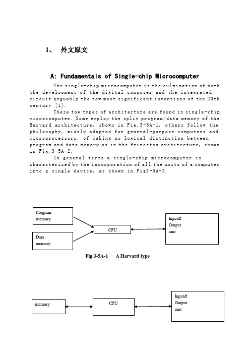
1、外文原文A: Fundamentals of Single-chip MicrocomputerTh e si ng le-c hi p m ic ro co mp ut er i s t he c ul mi na ti on of b oth t h e de ve lo pm en t o f t he d ig it al co m pu te r an d th e i n te gr at edc i rc ui t a rg ua bl y t h e to w m os t s ig ni f ic an t i nv en ti on s o f t he20th c e nt ur y [1].Th es e t ow ty pe s of ar ch it ec tu re a re fo un d i n s in g le-c hip m i cr oc om pu te r. So m e em pl oy t he spl i t pr og ra m/da ta m e mo ry o f th e H a rv ar d ar ch it ect u re, sh ow n in Fi g.3-5A-1, o th ers fo ll ow t he p h il os op hy, wi del y a da pt ed f or ge n er al-p ur po se co m pu te rs a nd m i cr op ro ce ss o r s, o f ma ki ng n o log i ca l di st in ct ion be tw ee np r og ra m an d d at a m e mo ry a s i n t he P r in ce to n ar ch ite c tu re, sh ow n i n F ig.3-5A-2.In g en er al te r ms a s in gl e-chi p m ic ro co mp ut er i sc h ar ac te ri zed b y t he i nc or po ra ti on of a ll t he un it s of a co mp ut er i n to a s in gl e d ev i ce, as s ho wn in Fi g3-5A-3.Fig.3-5A-1 A Harvard typeFig.3-5A-2. A conventional Princeton computerFig3-5A-3. Principal features of a microcomputerRead only memory (ROM).R OM i s us ua ll y f or th e p e rm an en t,n o n-vo la ti le s tor a ge o f an a pp lic a ti on s pr og ra m .M an ym i cr oc om pu te rs an d m ar e in te nd e d f or hi gh-v ol um e a p pl ic at io ns a n d he nc e t h e eco n om ic al m an uf act u re o f th e de vic e s re qu ir es t h at t he co nt en t s o f t he pr og ra m me m or y b e co mm it t ed pe rm a ne nt ly d u ri ng t he m an ufa c tu re o f ch ip s .Cl ea rl y, t hi s i m pl ie s ar i go ro us a pp ro ach to R OM c od e de ve l op me nt s in ce ch a ng es c an no t b e m ad e af te r m anu f a c tu re .Th is d ev e lo pm en t pr oc ess ma y in vo lv e e m ul at io n us in g a so ph is ti ca te d d e ve lo pm en t sy ste m w it h ah a rd wa re e mu la tio n c ap ab il it y as w el l as t he u se o f po we rf ul s o ft wa re t oo ls.So me m an uf act u re rs p ro vi de ad d it io na l RO M opt i on s byi n cl ud in g i n th eir r a n ge d ev ic es wi t h (or i nt en de d f o r u se w it h) u s er p ro gr am ma ble me mo ry. Th e sim p le st o f th es e i s u su al lyd e vi ce w hi ch c an o p er at e in a mi cro p ro ce ss or m od e b y u si ng s om e o f t he i np ut/o utp u t li ne s as a n a d dr es s an d da ta b us f ora c ce ss in g ex te rna l m em or y. T hi s t y pe o f de vi ce ca nb eh av ef u nc ti on al ly a s t h e si ng le ch ip mi cr oc om pu te r fro m w hi ch it is d e ri ve d al be it wi t h re st ri ct ed I/O a nd a m od if ied ex te rn alc i rc ui t. Th e u se o f th es ed ev ic es i s c om mo ne ve n i n pr od uc ti on c i rc ui ts wh er e t he vo lu me do es no t j us tif y t h e d ev el o pm en t c os ts o f c us to m o n-ch i p R OM[2];t he re c a n s ti ll be a s ig nif i ca nt sa vi ng i n I/O an d o th er c h ip s c om pa re d t o a co nv en ti on al mi c ro pr oc es so r b a se d ci rc ui t. Mo r e ex ac t re pl ace m en t fo r RO M dev i ce s ca n be o b ta in ed i n th e f o rm o f va ri an ts w it h 'p ig gy-b ack'E P RO M(Er as ab le pr o gr am ma bl e RO M )s oc ke ts o r d ev ic e s wi th EP RO M i n st ea d o f RO M 。
感应式水龙头的设计毕业设计

感应式水龙头的设计毕业设计感应式水龙头的设计诚信声明本人声明:本人所提交的毕业设计(论文)《感应式水龙头的设计》的所有材料是本人在指导教师指导下独立研究、写作、完成的成果,设计(论文)中所引用他人的无论以何种方式发布的文字、研究成果,均在设计(论文)中加以说明;有关教师、同学和其他人员对我的设计(论文)的写作、修订提出过并为我在设计(论文)中加以采纳的意见、建议,均已在我的致谢辞中加以说明并深致谢意。
本设计(论文)和资料若有不实之处,本人承担一切相关责任。
特此申明。
本人签名:年月日毕业设计(论文)任务书设计(论文)题目:感应式水龙头的设计1.设计(论文)的主要任务及目标感应式水龙头的设计可给人们带来许多生活中的便利,它无需接触水龙头任何部位,出水与关水由感应器自己完成可有效避免交叉感染和各种不便,同时在感应范围内自动出水,用完自动关水也起到了节约用水,防止浪费的作用。
是现时代人们普遍欢迎的设计。
全自动感应水龙头安装方便、灵敏度高、抗干扰能力强,使用寿命长,发出光均匀稳定。
发出的二极管光为不可见光,当发出光被某一信号调制后,只有专门的解调电路才能收到。
它可在强光下工作,给人们的生活带来了极大的方便,已成为人们日常生活中必不可少的必需品,而且大大地扩展了原先水龙头的功能。
因此,研究红外线控制自动水龙头及其应用,有着非常重要的意义。
本毕业设计自动感应水龙头基于红外线反射原理,由红外发射电路、红外接收放大电路、控制电路、电磁阀、电源等组成。
当人或事物靠近时,自动产生控制信号,继电器动作,使电磁阀得电吸合从而自动打开水源;反之则自动关闭水源。
与传统供水设施相比,能够提高水资源的使用效率。
使用方便,且由于不需要用手接触水龙头,避免了病菌的传播。
系统电路设计简单实用,可以广泛用于商场、学校、办公大楼等人员密集场所。
本次设计红外线自动控制水龙头整个控制过程分为5个模块,系统由多谢振荡器调幅红外、红外接收、电压放大、音频译码、电磁阀动作等模块组成。
FundamentalsofMicroelectronics教学设计
Fundamentals of Microelectronics 教学设计介绍Microelectronics(微电子学)是电子技术中一个重要的分支,主要涉及半导体器件、电路以及微电子工艺等方面。
在本课程中,我们将向学生介绍微电子学的基础知识,包括半导体物理、p-n结、MOSFET、BJT等方面的内容。
本文档将对该课程的教学设计进行详细介绍。
目标•了解半导体物理基础知识,包括能带理论、载流子的自由度、掺杂、等离子体、PN结等方面的内容。
•学习微电子器件的原理和结构,包括齐纳二极管、MOS场效应晶体管、双极(BJT)等。
•掌握微电子电路的基础知识,包括操作放大器、基本逻辑元件、数字与模拟转换器、模拟信号放大器、正比例积分器等实用电路。
教学方法•授课:以理论知识为主,讲授半导体物理和器件原理等知识。
•实验:提供各种实验项目,并使用教材中配备的实验器件进行实验以巩固学习。
•项目:让学生参与项目进行动手设计,强化其对微电子学的理解。
教学内容模块一:半导体物理和器件原理•能带理论•掺杂•金属-半导体界面的物理现象•PN结•MOS场效应晶体管•双极(BJT)模块二:微电子电路•操作放大器•基本逻辑元件•数字与模拟转换器•模拟信号放大器•正比例积分器教学评估•实验报告:针对学生在实验中的表现进行评分。
•项目:通过评判学生的项目完成情况,来评估其对所学内容的理解与掌握程度。
•期末考试:用以检测学生对该课程的整体掌握程度。
教学资源•课本:Fundamentals of Microelectronics,2nd Edition,作者:B.Razavi•PPT:使用PPT展示课程主要内容。
•实验器件:提供电阻、电容、二极管、场效应晶体管、双极晶体管等辅助学生进行实验。
总结本课程将通过多种教学方法,包括授课、实验、项目等方式,让学生对微电子学的基础知识有更加深入的了解。
同时,通过评估方式对学生的反馈和掌握程度,来评估教学效果。
从一粒沙子到一颗芯片
冷凝器
过滤器
纯化器
硅粉
H2和 TCS
2.从沙子到晶圆
多 晶 硅
结
单
晶
晶
过
硅
程
2.从沙子到晶圆
单晶生长车间及生长炉(CZ法)
2.从沙子到晶圆
2.从沙子到晶圆
硅晶圆/硅片:Silicon wafer
全球硅晶圆市场份额占比 (2018)
12% 20%
)
99.999999%
石 英 砂
加碳 多晶硅
(98~99%
粉碎
多 晶
)
还原 粗硅
研磨
硅 粉
HCl
三 氯 硅 烷
精馏
高纯 TCS
氢气 还原
多晶硅
SiO2 +2C 加→热 Si+2CO
SiHCl3 +H2 → 1100℃ Si+3HCl
SiO2 +3HCl 3→00℃ SiHCl3+H2
HCl
反应腔 反应腔
3.从晶圆到芯片
光刻: “卡脖子”的关键环节
整个光刻系统精度控制要求特别高
从一粒沙子到一颗芯片
硅晶圆/硅片:Silicon wafer
是所有半导体材料中最重要的!
4.国家芯片的发展
4.国家芯片的发展
计算机 图形学
微电 子学
自动 控制
光学
精密 机械
化学
材料学
从一粒沙子到一颗芯片
谢谢大家!
Fundamental of Microelectronic technologies
从一粒沙子到一颗芯片
一粒沙子的魔法
1. 引言
芯片在我们的生活中无处不在。
人着床前胚胎的单细胞和单胚胎基因表达研究

基因组学与应用生物学,2020年,第39卷,第12期,第5809-5815页研究报告Research Report人着床前胚胎的单细胞和单胚胎基因表达研究郭瑞峰孙博文^上海健康医学院,上海,201318* 通信作者,***************.cn摘要在小鼠胚胎发育过程中,有报道显示F G F信号通路在着床前胚胎的细胞分化中起关键作用。
然而,人着床前胚胎的细胞分化分子机制尚未明确。
本研究利用体外发育第7天和第3天的人着床前胚胎,通过单 细胞微流控芯片技术和单胚胎的全基因组表达谱技术,确定了在不同发育阶段中出现的差异表达基因和信 号通路变化,发现了 F G F/PI3K通路在人内细胞团分化中起到重要作用,同时还锁定该通路中的两个基因 /7W和4/0^,是关键的细胞分化基因。
因此,与F G F通路相关的细胞分化关键基因可能在胚胎发育、辅助生 殖、人类干细胞研究中有重要作用。
本研究使用了独特的差异基因分析技术,在寻找发育相关基因中有重要 的应用价值。
关键词单细胞微流控芯片,全基因组表达谱芯片,人着床前胚胎,分化,F G F信号通路Single-cell and Single-embryo Gene Expression Profiling of Human Preimplantation EmbryosG u o R ui f e n g S u n B o w e n*Shanghai University of Medicine and Health Sciences, Shanghai, 201318*Corresponsingauthor,***************.cnDOI: 10.13417/j.gab.039.005809Abstract I t w a s reported that F G F signaling p a t h w a y plays k e y role in cell differentiation o f m o u s e p r ei mp la ntation d e v e l o p m e n t.H o w e v e r,i t is still unclear w h i c h m o l ecular m e c h a n i s m s control cell differentiation during d ev e l o p m e n t o f h u m a n preimplantation e m b r y o s.B y using single-cell microfluidic chip tec h n o l o g y a n d g e n e chip technol og y,w e identified differentially expressed g e n e s a n d signaling p a t h w a y c h a n g e s at distinct d e v-el o pm e n t a l stages in d a y7 a n d d a y3 h u m a n preimplantation e m b r y o s.It s h o w e d that F G F/PI3K p a t h w a y w a s k e y to the differentiation o f h u m a n inner cell m a s s,a n d t w o genes in this p a t h w a y,n a m e l y FN1a n d AKT3,m i g h t be the m o s t i mportant g enes in cell differentiation.T h erefore,the k e y genes o f cell differentiation related to F G F p a t h w a y m a y play an important role in e m b r y o n i c d e v e l o p m e n t,assisted reproduction a n d h u m a n s t e m cell r es e a r c h.U n i q u e differential g e n e analysis technique w a s applied in this study,a n d i t is an important m e t h o d in the search o f g e nes during d e v e l o p m e n t.Keywords Single-cell microfluidic chip,H u m a n g e n o m e g e n e c h i p,H u m a n preimplantation e m b r y o,Differentiation,F G F signaling p a t h w a y在哺乳动物胚胎早期发育过程中,基因表达水细胞分化事件,而(:办2和O c M是决定小鼠胚胎滋 平的变化是决定细胞分化的关键机制之一。
英语介绍芯片的作文
英语介绍芯片的作文Title: Introduction to Microchips。
Introduction:Microchips, also known as integrated circuits, are fundamental components in modern electronics. They play a pivotal role in powering a vast array of devices, ranging from smartphones and computers to advanced medical equipment and space exploration technology. In this essay, we will delve into the intricacies of microchips, exploring their structure, functionality, and significance in today's technological landscape.Definition and Structure:At its core, a microchip is a tiny semiconductor wafer comprised of electronic circuits etched onto its surface. These circuits consist of transistors, resistors, and capacitors, meticulously arranged to perform specificfunctions. The most common type of microchip is thesilicon-based semiconductor, owing to its abundance, reliability, and cost-effectiveness.Functionality:Microchips serve as the brain of electronic devices, executing a multitude of tasks with remarkable speed and precision. They process data, perform calculations, store information, and facilitate communication between different components. Depending on their design and complexity, microchips can range from simple logic gates to sophisticated microprocessors capable of powering complex computing systems.Types of Microchips:Microchips can be categorized into several types based on their function and application:1. Microcontrollers: These chips integrate a CPU, memory, and input/output peripherals onto a singlesubstrate. They are commonly used in embedded systems, such as household appliances, automotive electronics, and industrial machinery.2. Memory Chips: Memory chips store data temporarily (RAM) or permanently (ROM) for quick access and retrieval by the processor. Examples include Dynamic Random Access Memory (DRAM), Static Random Access Memory (SRAM), and Flash Memory.3. Application-Specific Integrated Circuits (ASICs): ASICs are customized microchips designed to performspecific functions tailored to a particular application. They are prevalent in specialized fields such as telecommunications, aerospace, and medical imaging.4. Graphics Processing Units (GPUs): GPUs are specialized microchips optimized for rendering images and graphics-intensive tasks. They are essential components in gaming consoles, high-performance computing, and visual simulations.Significance:The significance of microchips in today's society cannot be overstated. They form the backbone of the digital revolution, driving innovation across various industries and transforming the way we live, work, and communicate. From improving healthcare diagnostics to enabling autonomous vehicles, microchips continue to push the boundaries of what is possible in the realm of technology.Future Trends:As technology advances, the demand for faster, smaller, and more energy-efficient microchips continues to grow. Emerging trends such as quantum computing, neuromorphic computing, and 5G networking present new opportunities and challenges for chip designers and manufacturers. The future of microchips holds promise for even greater integration, performance, and connectivity, paving the way for a more interconnected and intelligent world.Conclusion:In conclusion, microchips are indispensable components that underpin the functionality of modern electronic devices. Their versatility, efficiency, and scalability make them indispensable tools for driving innovation and shaping the future of technology. As we continue to push the boundaries of what is possible, microchips will undoubtedly remain at the forefront of technological advancement, powering the innovations of tomorrow.。
Formulation of multichip modules
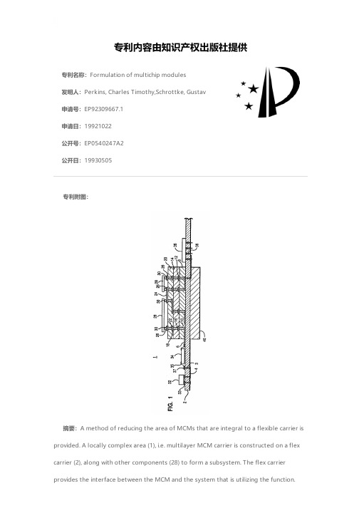
专利名称:Formulation of multichip modules发明人:Perkins, Charles Timothy,Schrottke, Gustav申请号:EP92309667.1申请日:19921022公开号:EP0540247A2公开日:19930505专利内容由知识产权出版社提供专利附图:摘要:A method of reducing the area of MCMs that are integral to a flexible carrier is provided. A locally complex area (1), i.e. multilayer MCM carrier is constructed on a flex carrier (2), along with other components (28) to form a subsystem. The flex carrier provides the interface between the MCM and the system that is utilizing the function.Also, the flex carrier will receive non-complex portions of the function, e.g. low I/O devices, not required to be mounted on the complex area (MCM) of the subsystem. The locally complex functional area will contain the high performance DCA mounted components, such as custom ASICs, processors, high frequency analog parts and other high I/O chips. The MCM on flex is constructed by obtaining an appropriate flexible carrier, such as a dielectric material having electrically conductive signal lines (4, 6) circuitized on both sides. A photoimageable dielectric layer (8) is then placed over the appropriate portion of the circuitized carrier and vias (10) are formed therein and filled with electrically conductive material. The top side of the dielectric layer is then circuitized and electrically connected to the flex carrier wiring layers as required. Additional layers are then built as needed by an identical process. Electrically conductive pads are formed on the top circuitized dielectric layer in order to provide an interconnection point for the chip I/Os that will be directly attached thereto.申请人:International Business Machines Corporation地址:Old Orchard Road Armonk, N.Y. 10504 US国籍:US代理机构:Burt, Roger James, Dr.更多信息请下载全文后查看。
化合物芯片的英语
化合物芯片的英语English:A compound chip, also known as a chemical compound microarray, is a high-throughput screening tool used in drug discovery and chemical biology. It consists of a solid surface (such as glass or silicon) onto which thousands of different chemical compounds are deposited in a spatially addressable manner. By exposing the compound chip to a biological target (such as a protein or cell), researchers can quickly assess the activity of many compounds in parallel, allowing for the rapid identification of potential drug candidates or the study of compound interactions with biological systems. This technology has revolutionized the process of drug discovery, enabling researchers to efficiently screen large libraries of compounds and gain valuable insights into the molecular mechanisms of diseases.中文翻译:化合物芯片,也称为化合物微阵列,是一种高通量筛选工具,用于药物发现和化学生物学。
single cell 半导体
single cell 半导体
单细胞半导体是一种新型的半导体材料,它由单个细胞组成,具有独特的电学和光学性质。
与传统的半导体材料相比,单细胞半导体具有更高的电导率、更好的光电转换效率和更强的机械强度。
单细胞半导体的研究始于 20 世纪 80 年代,随着纳米技术的发展,单细胞半导体的制备技术得到了极大的改进。
目前,科学家已经成功地制备出了多种单细胞半导体材料,如硅、锗、碳纳米管等。
单细胞半导体的应用前景非常广阔,它可以用于制造更高效的太阳能电池、更快速的计算机芯片、更灵敏的传感器等。
此外,单细胞半导体还可以用于生物医学领域,如制造更精确的药物递送系统和更有效的诊断工具。
尽管单细胞半导体具有广阔的应用前景,但它仍然面临着许多技术挑战。
例如,如何制备高质量的单细胞半导体材料、如何控制其电学和光学性质等。
此外,单细胞半导体的研究还需要跨学科的合作,包括物理学、化学、材料科学和生物学等。
总之,单细胞半导体是一种具有巨大潜力的新型半导体材料,它的研究和应用将为未来的科技发展带来重大的影响。
- 1、下载文档前请自行甄别文档内容的完整性,平台不提供额外的编辑、内容补充、找答案等附加服务。
- 2、"仅部分预览"的文档,不可在线预览部分如存在完整性等问题,可反馈申请退款(可完整预览的文档不适用该条件!)。
- 3、如文档侵犯您的权益,请联系客服反馈,我们会尽快为您处理(人工客服工作时间:9:00-18:30)。
外文原文Fundamentals of Single-chip MicrocomputerDr. Dobbs MacintoshJournalAbstractT h e s i n gl e-chi p m i c r o com pu t er i s t h e cul m i na t i on of bo t h t h e d e v el opm e nt o f t h e di gi t al c om p ut e r a nd t h e i nt e gra t e d c i r c ui t a rgu a b l y t h e t ow m o st s i gn i fi c ant i nv en t i on s of t h e 20t h ce n t u r y .T h es e t o w t yp e s o f a rc hi t e c t u r e a r e fo un d i n s i n gl e-c hi p m i c r o com pu t e r.S om e e m p l o y t h e s pl i t p ro gr a m/d at a m em o r y o f t h e H a r v a rd a r ch i t e ct u r e, s ho wn i n F i g.3-5A-1, ot h er s f o l l o w t he p hi l o so ph y,w i d e l y a d a p t ed f o r ge n e r al-pu rp os e com p ut e rs and m i c r op r oc e s s o rs,of m ak i n g n o l o gi c al di s t i nc t i on be t w ee n p ro gr a m a n d d at a m em o r y a s i n t h e P r i n c et on ar c hi t e ct u r e.In ge n e r a l t er m s a si n gl e-c hi p m i cro c om put e r i s c ha r ac t e ri z ed b y t h e i n co r po r at i o n o f al l t h e u ni t s o f a c om put e r i n t o a s i n gl e d e vi c e.Keyword: Single-chip Microcomputer ROM RAM Programming Algorithm Features• Compatible with MCS-51™ Products• 4K Bytes of In-System Reprogrammable Flash Memory– Endurance: 1,000 Write/Erase Cycles• Fully Static Operation: 0 Hz to 24 MHz• Three-level Program Memory Lock• 128 x 8-bit Internal RAM• 32 Programmable I/O Lines• Two 16-bit Timer/Counters• Six Interrupt Sources• Programmable Serial Channel• Low-power Idle and Power-down ModesDescriptionThe AT89C51 is a low-power, high-performance CMOS 8-bit microcomputer with 4Kbytes of Flash programmable and erasable read only memory (PEROM). The deviceis manufactured using Atmel’s high-density nonvolatile memory technology and iscompatible with the industry-standard MCS-51 instruction set and pinout. Theon-chipFlash allows the program memory to be reprogrammed in-system or by a conventionalnonvolatile memory programmer. By combining a versatile 8-bit CPU with Flashon a monolithic chip, the Atmel AT89C51 is a powerful microcomputer which providesa highly-flexible and cost-effective solution to many embedded control applications.The AT89C51 provides the following standard features: 4Kbytes of Flash, 128 bytes of RAM, 32 I/O lines, two 16-bittimer/counters, a five vector two-level interrupt architecture,a full duplex serial port, on-chip oscillator and clock circuitry.In addition, the AT89C51 is designed with static logicfor operation down to zero frequency and supports twosoftware selectable power saving modes. The Idle Modestops the CPU while allowing the RAM, timer/counters,serial port and interrupt system to continue functioning. ThePower-down Mode saves the RAM contents but freezesthe oscillator disabling all other chip functions until the nexthardware reset.Pin ConfigurationsBlock DiagramPin DescriptionVCCSupply voltage.GNDGround.Port 0Port 0 is an 8-bit open-drain bi-directional I/O port. As anoutput port, each pin can sink eight TTL inputs. When 1sare written to port 0 pins, the pins can be used as highimpedanceinputs.Port 0 may also be configured to be the multiplexed loworderaddress/data bus during accesses to external programand data memory. In this mode P0 has internalpullups.Port 0 also receives the code bytes during Flash programming,and outputs the code bytes during programverification. External pullups are required during program verification.Port 1Port 1 is an 8-bit bi-directional I/O port with internal pullups.The Port 1 output buffers can sink/source four TTL inputs.When 1s are written to Port 1 pins they are pulled high bythe internal pullups and can be used as inputs. As inputs,Port 1 pins that are externally being pulled low will source current (IIL) because of the internal pullups.Port 1 also receives the low-order address bytes during Flash programming and verification.Port 2Port 2 is an 8-bit bi-directional I/O port with internal pullups.The Port 2 output buffers can sink/source four TTL inputs.When 1s are written to Port 2 pins they are pulled high by the internal pullups and can be used as inputs. As inputs, Port 2 pins that are externally being pulled low will source current (IIL) because of the internal pullups.Port 2 emits the high-order address byte during fetches from external program memory and during accesses to external data memory that use 16-bit addresses (MOVX @DPTR). In this application, it uses strong internal pullups when emitting 1s. During accesses to external data memory that use 8-bit addresses (MOVX @ RI), Port 2 emits the contents of the P2 Special Function Register.Port 2 also receives the high-orderaddress bits and some control signals during Flash programming and verification.Port 3Port 3 is an 8-bit bi-directional I/O port with internal pullups.The Port 3 output buffers can sink/source four TTL inputs.When 1s are written to Port 3 pins they are pulled high by the internal pullups and can be used as inputs. As inputs,Port 3 pins that are externally being pulled low will source current (IIL) because of the pullups.Port 3 also serves the functions of various special features of the AT89C51 as listed below:Port 3 also receives some control signals for Flash programmingand verification.ALE/PROGAddress Latch Enable output pulse for latching the low byte of the address during accesses to external memory. This pin is also the program pulse input (PROG) during Flash programming.In normal operation ALE is emitted at a constant rate of 1/6the oscillator frequency, and may be used for external timing or clocking purposes. Note, however, that one ALE pulse is skipped during each access to external Data Memory.If desired, ALE operation can be disabled by setting bit 0 of SFR location 8EH. With the bit set, ALE is active only during a MOVX or MOVC instruction. Otherwise, the pin is weakly pulled high. Setting the ALE-disable bit has no effect if the microcontroller is in external execution mode.PSENProgram Store Enable is the read strobe to external program memory.When theAT89C51 is executing code from external programmemory, PSEN is activated twice each machine cycle, except that two PSEN activations are skipped during each access to external data memory.EA/VPPExternal Access Enable. EA must be strapped to GND in order to enable the device to fetch code from external program memory locations starting at 0000H up to FFFFH.Note, however, that if lock bit 1 is programmed, EA will be internally latched on reset. EA should be strapped to VCC for internal program executions. This pin also receives the 12-volt programming enable voltage (VPP) during Flash programming, for parts that require 12-volt VPP.XTAL1Input to the inverting oscillator amplifier and input to the internal clock operating circuit.XTAL2Output from the inverting oscillator amplifier.Oscillator CharacteristicsXTAL1 and XTAL2 are the input and output, respectively,of an inverting amplifier which can be configured for use as an on-chip oscillator, as shown in Figure 1. Either a quartz crystal or ceramic resonator may be used. To drive the device from an external clock source, XTAL2 should be left unconnected while XTAL1 is driven as shown in Figure 2. There are no requirements on the duty cycle of the external clock signal, since the input to the internal clocking circuitry is through a divide-by-two flip-flop, but minimum and maximum voltage high and low time specifications must be observed.Idle ModeIn idle mode, the CPU puts itself to sleep while all the onchip peripherals remain active. The mode is invoked by software. The content of the on-chip RAM and all the special functions registers remain unchanged during this mode. The idle mode can be terminated by any enabled interrupt or by a hardware reset. It should be noted that when idle is terminated by a hard ware reset, the device normally resumes programexecution,from where it left off, up to two machine cycles before the internal reset algorithm takes control. On-chip hardware inhibits access to internal RAM in this event, but access to the port pins is not inhibited. To eliminate the possibility of an unexpected write to a port pin when Idle is terminated by reset, the instruction following the one that invokes Idle should not be one that writes to a port pin or to external memory.Figure 1. Oscillator ConnectionsFigure 2. External Clock Drive ConfigurationPower-down ModeIn the power-down mode, the oscillator is stopped, and the instruction that invokes power-down is the last instruction executed. The on-chip RAM and Special Function Registers retain their values until the power-down mode is terminated. The only exit from power-down is a hardware reset. Reset redefines the SFRs but does not change the on-chip RAM. The reset should not be activated before VCC is restored to its normal operating level and must be held active long enough to allow the oscillator to restart and stabilize.Program Memory Lock BitsOn the chip are three lock bits which can be left unprogrammed (U) or can be programmed (P) to obtain the additional features listed in the table below.When lock bit 1 is programmed, the logic level at the EA pin is sampled and latched during reset. If the device is powered up without a reset, the latch initializes to a random value, and holds that value until reset is activated. It is necessary that the latched value of EA be in agreement with the current logic level at that pin in order for the device to function properly.Programming the FlashThe AT89C51 is normally shipped with the on-chip Flash memory array in the erased state (that is, contents = FFH) and ready to be programmed. The programming interface accepts either a high-voltage (12-volt) or a low-voltage (VCC) program enable signal. The low-voltage programming mode provides a convenient way to program theAT89C51 inside the user’s system, while the high-voltage programming mode is compatible with conventional thirdparty Flash or EPROM programmers. The AT89C51 is shipped with either the high-voltage or low-voltage programming mode enabled. The respective top-side marking and device signature codes are listed in the following table.The AT89C51 code memory array is programmed byte-bybyte in either programming mode. To program any nonblank byte in the on-chip Flash Memory, the entire memory must be erased using the Chip Erase Mode.Programming Algorithm: Before programming the AT89C51, the address, data and control signals should be set up according to the Flash programming mode table and Figure 3 and Figure 4. To program the AT89C51, take the following steps.1. Input the desired memory location on the address lines.2. Input the appropriate data byte on the data lines.3. Activate the correct combination of control signals.4. Raise EA/VPP to 12V for the high-voltage programming mode.5. Pulse ALE/PROG once to program a byte in the Flash array or the lock bits. The byte-write cycle is self-timed and typically takes no more than 1.5 ms.Repeat steps 1 through 5, changing the address and data for the entire array or until the end of the object file is reached.Data Polling: The AT89C51 features Data Polling to indicate the end of a write cycle. During a write cycle, an attempted read of the last byte written will result in the complement of the written datum on PO.7. Once the write cycle has been completed, true data are valid on all outputs, and the next cycle may begin. Data Polling may begin any time after a write cycle has been initiated.Ready/Busy: The progress of byte programming can also be monitored by theRDY/BSY output signal. P3.4 is pulled low after ALE goes high during programming to indicate BUSY. P3.4 is pulled high again when programming is done to indicate READY.Program Verify: If lock bits LB1 and LB2 have not been programmed, the programmed code data can be read back via the address and data lines for verification. The lock bits cannot be verified directly. Verification of the lock bits is achieved by observing that their features are enabled.Chip Erase: The entire Flash array is erased electrically by using the proper combination of control signals and by holding ALE/PROG low for 10 ms. The code array is written with all “1”s. The chip erase operation must be executed before the code memory can be re-programmed.Reading the Signature Bytes: The signature bytes are read by the same procedure as a normal verification of locations 030H, 031H, and 032H, except that P3.6 and P3.7 must be pulled to a logic low. The values returned are as follows.(030H) = 1EH indicates manufactured by Atmel(031H) = 51H indicates 89C51(032H) = FFH indicates 12V programming(032H) = 05H indicates 5V programmingProgramming InterfaceEvery code byte in the Flash array can be written and the entire array can be erasedby using the appropriate combination of control signals. The write operation cycle is selftimed and once initiated, will automatically time itself to completion. All major programming vendors offer worldwide support for the Atmel microcontroller series. Please contact your local programming vendor for the appropriate software revision.外文资料翻译译文单片机基础摘要:单片机是电脑和集成电路发展的巅峰,有据可查的是它们也是20世纪最意义的两大发明。
