麦克风阵列模块XFM10412数据手册
科大讯飞麦克风阵列模块 XFM10412 评估板使用说明说明书

科大讯飞麦克风阵列模块XFM10412评估板使用说明科大讯飞股份有限公司安徽省合肥市望江西路666号国家科技创新型试点市示范区科大讯飞语音产业基地一、简介科大讯飞模块XFM10412是一款基于4麦克风阵列的语音前端解决方案。
模块利用麦克风阵列的空域滤波特性,通过对唤醒人的角度定位,形成定向拾音波束,并对波束以外的噪声进行抑制,提升远场拾音质量、保证识别效果。
功能:180度声源定位、降噪、回声消除、语音唤醒二、包装清单编号类型数量1 评估板卡1块2 麦克板卡1块3 音频线1根4 USB电源线1根5 USB转串口数据线1根6 录音线1根7 评估板说明书1个三、实体图图1 四麦线性阵列评估板实体图四、硬件连接指南第一步:使用1根音频线把麦克板卡连接到评估板卡上;注意:麦克板卡对应连接到评估板卡上的J12。
第二步:USB转串口数据线的串口端连到评估板卡的UART1上,另一端USB端连接到PC的USB 接口上;第三步:使用USB电源线连接到评估板卡microUSB口(位号:P1)上进行供电;注意:不能使用电脑USB接口直接供电,请使用5V电压稳定电源供电,如:手机充电器等。
第四步:把耳机(自备)插入音频插座上;图2 硬件连接后的实物图五、快速体验为了让您快速体验,可以按照如下流程操作:第一步:打开PC上的SecureCRT工具,并配置串口参数在讯飞开放平台麦克风阵列页面下载的技术文档压缩包中,包含有此工具,可以下载后使用。
串口通信参数设置如下:波特率 115200;数据位 8;奇偶校验位无;停止位 1;流控无。
第二步:体验语音唤醒、声源定位、噪声抑制等说出唤醒词“灵犀灵犀”,这时评估板卡上的WakeUp指示灯点亮,在SecureCRT工具的界面上显示“WAKE UP! angle:xxx”,angle的数值表示语音唤醒位置的角度。
详见下图所示:图3 唤醒后的效果图图4 SecureCRT工具界面显示使用耳机可以直接听到处理后输出的音频。
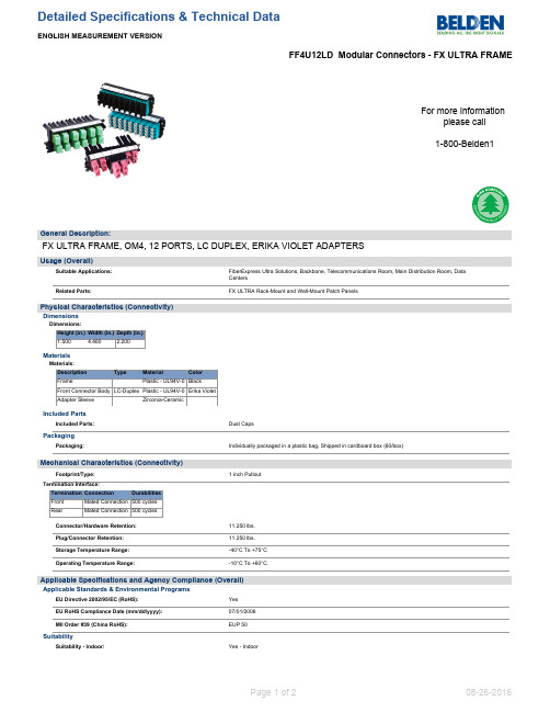
Belden FX Ultra 12端口LC双极接口OM4光纤框架说明书
Page 2 of 2
08-26-2016
Item # FF4U12LD
Putup 1 EA
Ship Weight 0.030 LB
Color
Notes
Item Desc FXU FRAME OM4 12P
Revision Number: 0 Revision Date: 11-07-2014
© 2016 Belden, Inc All Rights Reserved.
Related Parts:
FX ULTRA Rack-Mount and Wall-Mount Patch Panels
Physical Characteristics (Connectivity)
Dimensions Dimensions:
Height (in.) Width (in.) Depth (in.)
Mechanical Characteristics (Connectivity)
Footprint/Type:
Termination Interface:
Termination Connection
Durabilities
Front
Mated Connection 500 cycles
Rear
Mated Connection 500 cycles
1.500
4aterials:
Description
Type
Material
Color
Frame
Plastic - UL94V-0 Black
Front Connector Body LC-Duplex Plastic - UL94V-0 Erika Violet
来自ST的MEMS麦克风使用指南,含参数计算

February 2017DocID025704 Rev 2 1/20 AN4426 Application note Tutorial for MEMS microphonesIntroductionThis application note serves as a tutorial for MEMS microphones, providing general characteristics of these devices, both acoustic and mechanical, as well as summarizing the portfolio available from ST. MEMS microphones target all audio applications where small size, high sound quality, reliability and affordability are key requirements.ST's MEMS microphones are designed, developed and manufactured within ST, creating an industry-unique, vertically integrated supply chain. Both analog and digital-input, top and bottom-port solutions are available.Our best-in-class AOP and SNR make ST’s MEMS microphones suitable for applications that require a very high dynamic range, improving the audio experience in any environment. Matching very tightsensitivity allows optimizing beamforming and noise cancelling algorithms for multi-microphone arrays. Low power consumption allows extending battery life.Contents AN4426 Contents1Mechanical specifications, construction details (4)2Acoustic parameters (11)2.1Sensitivity (11)2.2Directionality (11)2.3SNR (12)2.4Dynamic range and acoustic overload point (12)2.5Equivalent input noise (13)2.6Frequency response (15)2.7Total harmonic distortion (16)2.8PSRR and PSR (16)3MEMS microphone portfolio (17)4Revision history (19)2/20 DocID025704 Rev 2AN4426 List of figures List of figuresFigure 1: MEMS microphone inside package (4)Figure 2: MEMS transducer mechanical specifications (4)Figure 3: Capacitance change principle (5)Figure 4: 4 x 5 package (5)Figure 5: 3 x 4 metal cap package - bottom port (6)Figure 6: 3 x 4 package - top port (6)Figure 7: 2 x 3 package - bottom port (7)Figure 8: Faraday cage in ST’s MEMS microphones (7)Figure 9: RF immunity simulation (8)Figure 10: EMC test setup (8)Figure 11: RF test disturbance signal with sinusoidal pattern (9)Figure 12: RF immunity test results - MP34DT04 (9)Figure 13: RF test disturbance signal @ 217 Hz burst pattern (10)Figure 14: RF immunity of analog differential microphones (10)Figure 15: Omnidirectional microphone (11)Figure 16: A-weighted filter response (12)Figure 17: Acoustic and electrical relationship - analog (13)Figure 18: Acoustic and electrical relationship - digital (14)Figure 19: MP45DT02-M frequency response (15)Figure 20: MEMS microphone portfolio (17)Figure 21: MEMS microphone notation (17)DocID025704 Rev 2 3/201 Mechanical specifications, construction detailsA microphone is a dual-die device consisting of two components, the integrated circuit andthe sensor, which are housed in a package using techniques that are proprietary to ST.ASICintegratedThe sensor uses MEMS technology (Micro-Electrical-Mechanical Systems) and it isbasically a silicon capacitor. The capacitor consists of two silicon plates/surfaces. Oneplate is fixed while the other one is movable (respectively, the green plate and the grey oneshown in the following figure). The fixed surface is covered by an electrode to make itconductive and is full of acoustic holes which allow sound to pass through. The movableplate is able to move since it is bonded at only one side of its structure. A ventilation hole,allows the air compressed in the back chamber to flow out and consequently allows themembrane to move back. The chamber allows the membrane to move inside but also, incombination with the chamber created by the package will affect the acoustic performanceof the microphones in terms of frequency response and SNR.Figure 2: MEMS transducer mechanical specificationsSo basically the microphone MEMS sensor is a variable capacitor where the transductionprinciple is the coupled capacitance change between a fixed plate (back plate) and amovable plate (membrane) caused by the incoming wave of the sound.4/20 DocID025704 Rev 2Figure 3: Capacitance change principleThe integrated circuit converts the change of the polarized MEMS capacitance into a digital (PDM modulated) or analog output according to the microphone type. Finally the MEMS microphone is housed in a package with the sound inlet placed in the top or in the bottom part of the package, hence the top-port or bottom-port nomenclature of the package. ST manufactures microphones using industry-wide techniques, but also has developed innovative packaging to achieve improved performance of the microphones. Packaging techniques will be discussed in further detail.The 4x5 package is widely used to house the digital microphone MP45DT02-M. It is a common packaging technique in a top-port configuration where the ASIC is placed under the sound inlet with glue on top (glob top) in order to protect the circuit from light and the MEMS sensor is placed beside the integrated circuit. The two silicon components are fixed to the substrate and the pads of the device are on the bottom side. The resonant chambers are identified depending on the position of each chamber with respect to the membrane and the incoming sound. In this case, considering the incoming direction of the sound, the front chamber is created by the package and the chamber inside the MEMS, behind the MEMS membrane, is the back chamber. This configuration allows protecting the MEMS from dust and particles falling into the package but results in a low SNR and frequency response with a peak in the audio band.Figure 4: 4 x 5 packageThe 3x4 package is used in ST to produce both the bottom and the top-port digital microphones, MP34DB02 and MP34DT01-M, MP34DT04/-C1, and MP34DT05. Considering the bottom configuration first, this structure is depicted in the following figure. The ASIC and the MEMS sensor are fixed to the substrate and the pads of the device are on bottom side as well. The sound inlet is obtained by drilling the substrate according to the position of the MEMS sensor. The package encloses all the components. In this configuration the front chamber is the cavity of the MEMS sensor and the package creates the back chamber. This design optimizes the acoustic performance of the microphone in terms of SNR and also allows obtaining a flat response across the entire audio band. The drawback of this solution is represented by the assembly of this microphone. Usually theDocID025704 Rev 2 5/20bottom-port microphones are soldered on the PCB. The thickness of the board modifies thevolume of the front chamber, degrading the flat response of this type of microphone (referto AN4427, “Gasket design for optimal acoustic performance in MEMS microphones” fordetails). In order to minimize the artifacts caused by this environment, a flex cable isrecommended to be used. Additionally, the bottom-port microphones have a ringed metalpad around the hole. A very careful soldering process is required to avoid dust or solderingpaste from entering in the sound port, damaging the MEMS membrane.Figure 5: 3 x 4 metal cap package - bottom portThe 3x4 top-port configuration is basically a mirrored bottom-port microphone. The ASICand the sensor are placed close to each other, the sensor is still under the sound inlet butthese two components are attached to the top of the structure, in other words, the ASICand MEMS are fixed to the package lid, not to the substrate. The pads are on the substrateand thus on the bottom side of the microphone. This configuration, covered by ST patents,allows optimizing all the benefits of the bottom-port microphone in terms of acousticperformance (i.e. maximized SNR and flat band) and all the benefits related to the top-portconfiguration during the assembly process.Figure 6: 3 x 4 package - top port6/20 DocID025704 Rev 2A smaller package, 2.5 x 3.35 mm, has been introduced in ST's product portfolio (for simplicity referred to as 2x3, see Figure 7: "2 x 3 package - bottom port"). This package is a bottom-port configuration with the same internal construction as the 3 x 4 bottom-port package and it is used for the analog differential microphones MP23AB01DM/DH and analog single-ended microphone MP23AB02B. As a result of the 2x3 bottom-port package and differential output configuration, the MP23AB01DH is the best microphone provided by ST in terms of SNR and AOP.Figure 7: 2 x 3 package - bottom portMEMS microphones housed in a plastic package are protected from radiated disturbances by embedding in the plastic package a metal shield which serves as a Faraday cage. The model in the following figure shows how the Faraday cage is implemented in ST’s plastic packages.Figure 8: Faraday cage in ST’s MEMS microphonesThe next figure shows the simulation of an electric field in open space. By applying an electric field source outside the microphone package, the Faraday cage is able to considerably attenuate the field inside the microphone structure. The temperature grade of the E field is an easy way to plot the results.DocID025704 Rev 2 7/20Figure 9: RF immunity simulationIn addition to the simulation, ST has a dedicated test to evaluate immunity, “Microphonedurability to EMC disturbances”.Microphones are subjected to RF disturbances using a proper jig with the following setup.Basically the test consists of placing the microphone under an antenna radiating adisturbance signal of 1 kHz AM modulated in the range [0.8, 3] GHz. The RF amplitudediffers depending on the frequency range according to the following criteria:•+33 dBm in the range [0.8, 2.4]•+17 dBm in the range [2.4, 3.0]8/20 DocID025704 Rev 2Figure 11: RF test disturbance signal with sinusoidal patternThe carrier of the disturbance is 1 kHz since it is an audio signal. Hence, the RF immunity of the microphone is evaluated by measuring the residual of the carrier at the output of the microphone. The next figure shows the result of the peak at 1 kHz measured when applying the RF disturbance on top of an MP34DT04.In parallel with the sinusoidal pattern, another 217 Hz burst pattern used to test the RF immunity is shown in the following figure.•The RF amplitude (power): +33 dBm•Carrier frequency: 700 MHz ~ 2.5 GHz•GSM burst frequency: 217 Hz pattern (see below)DocID025704 Rev 2 9/20Figure 13: RF test disturbance signal @ 217 Hz burst patternFigure 14: RF immunity of analog differential microphones10/20 DocID025704 Rev 2AN4426Acoustic parametersDocID025704 Rev 211/202Acoustic parameters2.1SensitivityThe sensitivity is the electrical signal at the microphone output to a given acoustic pressure as input. The reference of acoustic pressure is 1 Pa or 94 dBSPL @ 1 kHz. The sound pressure level, expressed in decibel, dBSPL=20*Log(P/Po) where Po = 20 µPa is the threshold of hearing. 20*Log(1Pa/20µPa) = 94 dBSPL • For analog microphones the sensitivity is expressed in mV RMS /Pa or dBV/Pa •For digital microphones the sensitivity is expressed in dBFSdBV ≠ dBFS. It is not correct to compare different units. As given in the above equations, dBV is in reference to 1V RMS instead of dBFS where the reference is the digital full scale.2.2 DirectionalityThe directionality indicates the variation of the sensitivity response with respect to thedirection of the arrival of the sound. MEMS microphones from ST are omnidirectional which means that there is no sensitivity change to every different position of the source of thesound in space. The directionality can be indicated in a Cartesian axis as sensitivity drift vs. angle or in a polar diagram showing the sensitivity pattern response in space.The following figure depicts the directionality in these two reference systems.Figure 15: Omnidirectional microphoneAcoustic parametersAN442612/20DocID025704 Rev 22.3 SNRThe signal-to-noise ratio specifies the ratio between a given reference signal to the amount of residual noise at the microphone output. The reference signal is the standard signal at the microphone output when the sound pressure is 1Pa @ 1 kHz (microphone sensitivity). The noise signal (residual noise) is the microphone electrical output at silence.This parameter includes both the noise of the MEMS element and the ASIC. Concerning this sum, the main contribution to noise is given by the MEMS sensor, the integrated circuit contribution can be considered negligible. Typically, the noise level is measured in an anechoic environment and A-weighting the acquisition. The A-weighted filter corresponds to the human ear frequency response.Figure 16: A-weighted filter response2.4 Dynamic range and acoustic overload pointThe dynamic range is the difference between the minimum and maximum signal that the microphone is able to generate as output. • The minimum signal is the smallest audio signal that the microphone can generate distinctly from noise. In other words, the minimum signal is equivalent to the residual noise.•The maximum audio signal is that which the microphone can generate withoutdistortion. It is also called acoustic overload point (AOP). Actually, the specification allows up to 10% in terms of distortion at the acoustic overload point.AN4426 Acoustic parameters2.5 Equivalent input noiseA microphone is a sound-to-electricity transducer which means that any output signalcorresponds to a specific sound as input. The equivalent input noise (EIN) is the acousticlevel, expressed in dBSPL, corresponding to the residual noise as output.For example, a digital microphone with a sensitivity of -26 dBFS and a 63 dB as SNR:Residual noise = -26 - 63 = -89 dBFS this sum transposed in the acoustic domain is:EIN = 94 - 63= 31 dBSPLThe following figures summarize the relationship between the acoustic and electricdomains related to each of the parameters listed above. Figure 17: "Acoustic and electricalrelationship - analog" and Figure 18: "Acoustic and electrical relationship - digital" illustratethis for analog and digital microphones, respectively.Figure 17: Acoustic and electrical relationship - analogDocID025704 Rev 2 13/20Acoustic parametersAN442614/20DocID025704 Rev 29030-90-3094dBSPL AOPS N R =63d B-26dBFSD y n a m i c R a n g e =89d BSensitivity EIN Residual noiseAN4426 Acoustic parameters 2.6 Frequency responseThe frequency response of a microphone in terms of magnitude indicates the sensitivityvariation across the audio band. This parameter also describes the deviation of the outputsignal from the reference 0 dB. Typically, the reference for this measurement is exactly thesensitivity of the microphone @ 0 dB = 94 dBSPL @ 1 kHz. The frequency response of amicrophone can vary across the audio frequency band depending on three parameters: theventilation hole, the front chamber geometry, and back chamber geometry. The ventilationhole and the back chamber geometry have an impact on the behavior at low frequencieswhile the behavior at high frequencies depends on the geometry of the front chamber only.Behavior at high frequencies can be a resonance peak caused by the Helmholtz effect.This resonance is the phenomenon of air resonance in a cavity. As a matter of fact, itdepends on the dimension of the front chamber of the microphone, representing the soundcavity in which the air resonates. A microphone with a flat frequency response is suitablewhen natural sound and high intelligibility of the system is required. The following figureshows the response of the MP45DT02-M. It shows a roll-off at low frequencies and a peakaround 18 kHz caused by the large front chamber of this microphone.Figure 19: MP45DT02-M frequency responseThe frequency response of a microphone in terms of phase indicates the phase distortionintroduced by the microphone. In other words, the delay between the sound wave movingthe microphone membrane and the electrical signal at the microphone output results in thatthis parameter includes both the distortion due to the membrane and the ASIC.DocID025704 Rev 2 15/20Acoustic parametersAN442616/20DocID025704 Rev 22.7 Total harmonic distortionTHD is the measurement of the distortion affecting the electrical output signal of themicrophone given an undistorted acoustic signal as input. THD+N is expressed as a ratio of the integer in a specified band of the power of the harmonics plus the power of noise and the power of the undistorted signal (fundamental). Equation 1TTTTTT +NN (%)=∑PPPPPPPPPP (TTHHPPHHPPHHHH HH HH )+PPPPPPPPPP (NNPPHH HH PP )NN nn−1PPPPPPPPPP (FFFFHHFFHHHHPPHHFFHHFF )Typically ST indicates the THD+N measured in the (50 Hz - 4 kHz) band for a given undistorted signal 1 kHz @ 100 dBSPL.2.8 PSRR and PSRPSRR indicates the capability of the ASIC to reject noise added to the supply voltage. To evaluate this parameter, a tone of V IN = 100 mVpk-pk @ 217 Hz (GSM switching frequency in phone applications) is added to the power supply and then the amplitude of the output is measured. The added noise can be either a square wave or sinusoidal wave. Typically the square wave is preferred since it is the worst case.PSRR is the ratio of the residual noise amplitude at the microphone output (V OUT @ 217 Hz) to the added spurious signal on the supply voltage. It is typically expressed in dB as given in the equation below: Equation 2PPPPPPPP =20 xx log �(VV OOOOOO @217TTHH )(VV IINN @217TTHH )�The capability of the integrated circuit to reject noise added to the supply voltage can also be expressed with another parameter that is the PSR. Basically it is simply a measurement of the output when noise of 100 mVpk-pk @ 217 Hz is superposed to the supply voltage. Consequently expressed in dB as given in the equation below: Equation 3 PPPPPP =20 xx log[VV OOOOOO @217TTHH ]To evaluate either the PSRR or PSR, proper sealing of the sound inlet or measurements performed in an anechoic chamber are recommended to avoid mixing the superimposed noise with that of the noise floor of the output. Finally, in the microphone datasheets PSR is commonly given instead of PSRR.AN4426 MEMS microphone portfolio3 MEMS microphone portfolioFigure 20: MEMS microphone portfolioST’s portfolio includes digital and analog microphones. The commercial products arenamed using the notation depicted in the following figure.Figure 21: MEMS microphone notationDocID025704 Rev 2 17/20MEMS microphone portfolio AN442618/20DocID025704 Rev 2The following table provides a complete overview of the microphones offered by ST. Additionally it serves as a summary for selecting the appropriate microphone among the ST portfolio as the features of both digital and analog microphones are given.Table 1: Features of MEMS microphonesParameter MP45DT02-M MP34DB02 MP34DT01-M MP34DT04 MP34DT04-C1 MP34DT05 MP23AB02B MP23AB01DM MP23AB01DH Sensitivity -26 dBFS -26 dBFS -26 dBFS -26 dBFS -26 dBFS -26 dBFS -38 dBV -38 dBV -38 dBV Directivity OmnidirectionalOmnidirectional OmnidirectionalOmnidirectionalOmnidirectionalOmnidirectionalOmnidirectionalOmnidirectionalOmnidirectionalSNR 61 dB 62.5 dB 61 dB 64 dB 64 dB 64 dB 64 dB 64 dB 65 dB AOP 120 dBSPL 120 dBSPL 120 dBSPL 120 dBSPL 120 dBSPL 122 dBSPL 125 dBSPL 130 dBSPL 135 dBSPL EIN 33 dB 31.5 dB 33 dB 30 dB 30 dB 30 dB 30 dB 30 dB 29 dB THD+N <5% @ 115 dBSPL <5% @ 115 dBSPL <2% @ 115 dBSPL <5% @ 115 dBSPL <5% @ 115 dBSPL <6% @ 120 dBSPL <2% @ 120 dBSPL <10% @ 130 dBSPL <5% @ 130 dBSPL PSR -70 dB -86 dB -70 dB -70 dB -70 dB -72 dB -70 dB -85 dB -100 dB Max. current consumption 650 µA 650 µA 600 µA 700 µA 700 µA 650 µA 220 µA 250 µA 250 µA Package dimensions 3.76x4.76x1.25mm3x4x1mm 3x4x1.06mm 3x4x1.095mm 3x4x1.095mm 3x4x1mm 2.5x3.35x0.98mm 2.5x3.35x0.98mm 2.5x3.35x0.98mm Port location Top port Bottom port Top port Top port Top port Top port Bottom port Bottom port Bottom port Operating temperature-30°C<T<+85°C-40°C<T<+85°C-40°C<T<+85°C-40°C<T<+85°C-40°C<T<+85°C-40°C<T<+85°C-40°C<T<+85°C-40°C<T<+85°C-40°C<T<+85°CAN4426Revision historyDocID025704 Rev 219/204 Revision historyTable 2: Document revision historyDate RevisionChanges09-Jan-20141Initial release14-Feb-2017 2Updated part numbers throughout documentUpdated "Introduction" and Section 1: "Mechanical specifications, construction details"Updated Figure 5: "3 x 4 metal cap package - bottom port", Figure 20: "MEMS microphone portfolio", Figure 21: "MEMS microphone notation"Added Figure 7: "2 x 3 package - bottom port",Figure 13: "RF test disturbance signal @ 217 Hz burst pattern", Figure 14: "RF immunity of analog differential microphones" Updated Table 1: "Features of MEMS microphones"AN4426IMPORTANT NOTICE – PLEASE READ CAREFULLYSTMicroelectronics NV and its subsidiaries (“ST”) reserve the right to make changes, corrections, enhancements, modifications, and improvements to ST products and/or to this document at any time without notice. Purchasers should obtain the latest relevant information on ST products before placing orders. ST products are sold pursuant to ST’s terms and conditions of sale in place at the time of order acknowledgement.Purchasers are solely responsible for the choice, selection, and use of ST products and ST assumes no liability for application assistance or the design of Purchasers’ products.No license, express or implied, to any intellectual property right is granted by ST herein.Resale of ST products with provisions different from the information set forth herein shall void any warranty granted by ST for such product.ST and the ST logo are trademarks of ST. All other product or service names are the property of their respective owners.Information in this document supersedes and replaces information previously supplied in any prior versions of this document.© 2017 STMicroelectronics – All rights reserved20/20 DocID025704 Rev 2。
博根通信MIC2S电子平衡麦克风输入模块说明书
Priority Level*
This module can respond to 4 different levels of priority. Priority 1 is the highest priority. It mutes modules with lower priorities and is never muted. Priority 2 can be muted by Priority 1 modules and mutes modules set for 3 or 4. Priority 3 is muted by either Priority 1 or 2 modules and mutes Priority 4 modules. Priority 4 modules are muted by all higher priority modules.
J7 J5 J6
J4
J3
Gate
Controls the minimum necessary input signal level to turn the module’s output on and apply signal to the main unit's buses. Clockwise rotation increases the necessary signal level required to produce output as well as the signal threshold necessary to cause the module to mute other modules.
RME DMC-842数字传声器接口用户手册说明书

用户手册DMC-842数字传声器接口带有线路(Line)输出的8通道数字传声器接口8通道AES转模拟/ADAT接口AES/EBU格式和采样率转换可选的64通道MADI接口24 Bit / 192 kHz数字音频MIDI远程控制重要的安全说明 (4)概述 (5)1. 简介 (6)2. 包装清单 (6)3. 简介及主要特点 (6)4. 首次使用——快速上手 (7)4.1 控制、接口与显示 (7)4.2 快速上手 (9)5. 附件 (9)6. 产品保证 (10)7. 附录 (10)CE / FCC符合性声明 (11)使用和操作 (12)8. 前面板控制 (13)8.1 Select(选择)键和旋钮(SET) (13)8.2 Clock Section(时钟部分) (14)8.3 模拟输出 (14)8.4 Remote(遥控) (15)9. 输入通道 (15)9.1 通用 (15)9.2 Gain(增益) (15)9.3 数字幻象供电 (15)9.4 Mode 2 (16)9.5 Stereo / Inactive (16)9.6 M/S处理 (16)9.7 SRC(采样率转换器) (17)9.8 PAR (17)9.9 Sync (17)10. Setup(设置)菜单 (18)10.1 通用 (18)10.2 ID(Id,自动ID) (18)10.3 Bank(bA,库) (18)10.4 Auto ID(Au,自动ID) (19)10.5 Delay Compensation(dC,延迟补偿) (19)10.6 Follow Clock(FC,跟随时钟) (20)10.7 Word Clock Out(Co,字时钟输出) (20)10.8 Peak Hold(Ph,峰值保持) (20)10.9 Digital Output(do,数字输出) (20)10.10 Analog Output(Ao,模拟输出) (21)10.11 Gain(GA,增益) (21)10.12 Control Pulse(Cp,控制脉冲) (21)10.13 Sync Pulse(SP,同步脉冲) (21)10.14 Special(SPECIAL) (22)11. Parameter(参数)菜单 (22)11.1 通用 (22)11.2 Low Cut(Lo-Cut,低切) (23)11.3 Directivity Pattern(PAttErn,指向性图) (23)11.4 Pre-Attenuation(AttEnuAtIon,预先衰减) (23)11.5 Mute(mute,静音) (23)11.6 Peak Limiter(LImItEr,峰值限制器) (23)11.7 Command Type(ComtyPE,命令类型) (23)12. Remote Control(远程控制) (24)12.1 MIDI (24)12.2 MIDI over MADI(借助MADI的MIDI) (24)12.3 Remote Control Software(远程控制软件) (25)12.4 RS232 (26)输入和输出 (27)13. 数字输入 (28)13.1 XLR (28)13.2 D-Sub - AES/EBU Sync(同步) (28)14. 数字输出 (29)14.1 AES/EBU (29)14.2 ADAT光纤 (30)14.3 I64 MADI卡 (31)14.4不同的MADI系列可配置I64 MADI卡和ADI-642 (32)15. 模拟输出 (33)16. 字时钟 (34)16.1 字时钟输入和输出 (34)16.2 技术描述和使用 (35)16.3 布线和终止 (36)17. MIDI (36)技术参考资料 (37)18. 技术指标 (38)18.1 模拟 (38)18.2 数字输入 (38)18.3 数字输出 (40)18.4 数字 (40)18.5 MIDI (40)18.6 通用 (41)18.7 固件 (41)18.8 MADI用户比特位 (41)18.9 接口针脚 (41)19. 技术背景 (43)19.1 术语 (43)19.2 锁定(Lock)与SyncCheck(同步检查) (44)19.3 延时(Latency)与监听(Monitoring) (45)19.4 DS –双倍速 (46)19.5 QS –四倍速 (46)19.6 AES/EBU - SPDIF (47)19.7 MADI基础 (48)19.8 SteadyClock(稳定时钟) (49)20. 框图 (50)21. DMC-842的MIDI实现 (51)21.1 基本SysEx格式 (51)21.2 通知类型–命令 (51)21.3 表格 (53)重要的安全说明注意! 不要打开底盘,以防触电。
nRF2401无线模块产品说明书

3.1 配置文件 ..................................................................................... 4 3.2 驱动文件 ..................................................................................... 6
2. 硬 件 模 块 说 明
nRF2401 无线模块产品说明书
图 1 nRF2401 丝印图
2.1 NRF2401 及其外围电路
nRF2401 及其外围电路如图 2 所示,包括 nRF2401 芯片部分、稳压部分、晶振部分、天线部分。电 压 VDD 为芯片提供工作电压;晶振部分包括 Y1、C11、C12,晶振 Y1 允许值为:4MHz、8MHz、12MHz、 16MHz,如果需要 1Mbps 的通信速率,则必须选择 16MHz 晶振。天线部分包括电感 L1、L2、L3(板子 自身天线)或者 L1、L3、ANT2(外接天线),用来将 nRF2401 芯片 ANT1、ANT2 管脚产生的 2.4G 电平 信号转为电磁波信号,或者将电磁波信号转换为电平信号输入芯片的 ANT1、ANT2 管脚。
R3 330 PWR_UP
VDD
CE CLK2 DATA2 CS
R5 330 R6 330 R7 330 R8 330
ADMP441 Rev. B 多向麦克风数据手册说明书

IVSEVINMP441FX EVAL-ADMP441Z EVAL-ADMP441Z-FLEXOmnidirectional Microphone withBottom Port and I 2S Digital OutputData SheetADMP441Rev. BDocument FeedbackInformation furnished by Analog Devices is believed to be accurate and reliable. However , noresponsibility is assumed by Analog Devices for its use, nor for any infringements of patents or other rights of third parties that may result from its use. Specifications subject to change without notice. No license is granted by implication or otherwise under any patent or patent rights of Analog Devices. T rademarks and registered trademarks are the property of their respective owners.O ne Technology Way, P.O. Box 9106, Norwood, MA 02062-9106, U.S.A. Tel: 781.329.4700 ©2011–2012 Analog Devices, Inc. All rights reserved. Technical Support FEATURESDigital I²S interface with high precision 24-bit data High SNR of 61 dBAHigh sensitivity of −26 dBFSFlat frequency response from 60 Hz to 15 kHz Low current consumption of 1.4 mA High PSR of −75 dBFSSmall 4.72 mm × 3.76 mm × 1 mm surface-mount package Compatible with Sn/Pb and Pb-free solder processes RoHS/WEEE compliantAPPLICATIONSTeleconferencing systems Gaming consoles Mobile devices Laptops TabletsSecurity systemsFUNCTIONAL BLOCK DIAGRAMG N G N G N V D L /C H I P E 09568-001Figure 1.BOTTOMTOP09568Figure 2. Isometric Views of ADMP441 Microphone PackageGENERAL DESCRIPTIONThe ADMP4411 is a high performance, low power, digital output, omnidirectional MEMS microphone with a bottom port. The complete ADMP441 solution consists of a MEMS sensor, signal conditioning, an analog-to-digital converter, antialiasing filters, power management, and an industry standard 24-bit I²S inter-face. The I²S interface allows the ADMP441 to connect directly to digital processors, such as DSPs and microcontrollers, with-out the need for an audio codec in the system.The ADMP441 has a high SNR and high sensitivity, making it an excellent choice for far field applications. The ADMP441 has a flat wideband frequency response, resulting in natural sound with high intelligibility.The ADMP441 is available in a thin 4.72 mm × 3.76 mm × 1 mm surface-mount package. It is reflow solder compatible with no sensitivity degradation. The ADMP441 is halide free.1Protected by U.S. Patents 7,449,356; 7,825,484; 7,885,423; and 7,961,897. Other patents are pending.OBS OL E T EADMP441Data SheetRev. B | Page 2 of 16TABLE OF CONTENTSFeatures .............................................................................................. 1 Applications ....................................................................................... 1 Functional Block Diagram .............................................................. 1 General Description ......................................................................... 1 Revision History ............................................................................... 2 Specifications ..................................................................................... 3 I²S Digital Input/Output .............................................................. 4 Timing Diagram ........................................................................... 4 Absolute Maximum Ratings ............................................................ 5 ESD Caution .................................................................................. 5 Pin Configuration and Function Descriptions .. (6)Typical Performance Characteristics ............................................. 7 Theory of Operation ........................................................................ 8 Understanding Sensitivity ............................................................8 Power Management.......................................................................8 Startup .............................................................................................8 I²S Data Interface ..........................................................................8 Digital Filter Characteristics ..................................................... 10 Applications Information .............................................................. 11 Power Supply Decoupling ......................................................... 11 Handling Instructions................................................................ 11 Supporting Documentation ...................................................... 11 Layout and Design Recommendations ........................................ 12 Outline Dimensions ....................................................................... 13 Ordering Guide .. (13)REVISION HISTORY10/12—Rev. A to Rev. BChanges to General Description Section ...................................... 1 Changes to P ick-and-Place Equipment Section, Evaluation Board User Guide Section, Circuit Note Section, andApplication Note Section (11)1/12—Rev. 0 to Rev. AChanges to Circuit Note Title ....................................................... 11 Updated Outline Dimensions ....................................................... 13 Deleted Figure 18 . (13)10/11—Revision 0: Initial VersionOBS OL E T EData SheetADMP441Rev. B | Page 3 of 16SPECIFICATIONST A = 25°C, V DD = 2.4 V , SCK = 3.072 MHz, SPL = 104 dB (3.16 Pa rms), unless otherwise noted. All minimum and maximum specifications are guaranteed. Typical specifications are not guaranteed. Table 1.Parameter Symbol Test Conditions/Comments Min Typ Max Unit PERFORMANCEDirectionalityOmniSensitivity at 94 dB SPL 1 1 kHz, 104 dB SPL−29 −26 −23 dBFS Signal-to-Noise Ratio SNR 20 kHz bandwidth, A-weighted 61 dBA Equivalent Input Noise EIN 20 kHz bandwidth, A-weighted33 dBA SPL Dynamic RangeDerived from EIN and maximum acoustic input 87 dB Frequency Response 2 Low frequency –3 dB point 60 Hz High frequency –3 dB point15 kHzDeviation limits from flat response within pass band −3/+2 dB Total Harmonic Distortion THD 104 dB SPL3 % Power Supply Rejection PSR 217 Hz, 100 mV p-p square wave superimposed on V DD −75 dBFS Maximum Acoustic Input Peak120 dB SPL Noise Floor 20 Hz to 20 kHz, A-weighted, rms −87 dBFS POWER SUPPLY Supply Voltage V DD 1.8 3.3 V Supply Current I DD V DD = 1.8 VNormal Mode 1.4 1.6 mA Standby 0.8 mA Power-Down 2 µA V DD = 3.3 VNormal Mode 2.2 2.5 mA Standby 0.8 mA Power-Down 4.5 µA DIGITAL FILTERGroup Delay17.25/f S sec f S = 48 kHz 359 µsf S = 16 kHz 1078µs Pass-Band Ripple±0.04 dB Stop-Band Attenuation60 dB Pass Band0.423 × f S20.3 kHz1The peak-to-peak amplitude is relative to peak-to-peak amplitude of 224 − 1. The stimulus is a 104 dB SPL sinusoid having rms amplitude of 3.1623 Pa. Sensitivity is relative to 1 Pa. 2See Figure 6 and Figure 8.OBS OL E T EADMP441Data SheetRev. B | Page 4 of 16I²S DIGITAL INPUT/OUTPUT–40°C < T A < +85°C, 1.8 V < V DD < 3.3 V , unless otherwise noted. Table 2.Limit 1Parameter Symbol Test Conditions/Comments Min Max Unit DIGITAL INPUTVoltage Input Low (L/R, WS, SCK) V IL 00.25 × V DDV Voltage Input High (L/R, WS, SCK) V IH 0.7 × V DD V DD V SD DIGITAL OUTPUTVoltage Output Low V OL V DD = 1.8 V, I SINK = 0.25 mA 0.1 × V DD V Voltage Output Low V OL V DD = 1.8 V, I SINK = 0.7 mA0.3 × V DD V Voltage Output High V OH V DD = 1.8 V, I SINK = 0.7 mA 0.7 × V DD V Voltage Output High V OH V DD = 1.8 V, I SINK = 0.25 mA 0.9 × V DDV Voltage Output Low V OL V DD = 3.3 V, I SINK = 0.5 mA 0.1 × V DD V Voltage Output Low V OL V DD = 3.3 V, I SINK = 1.7 mA0.3 × V DD V Voltage Output High V OH V DD = 3.3 V, I SINK = 1.7 mA 0.7 × V DD V Voltage Output HighV OH V DD = 3.3 V, I SINK = 0.5 mA0.9 × V DDV1Limits based on characterization results; not production tested.Table 3. Serial Data Port Timing SpecificationsParameter Description Min Max Unit t SCH SCK high 50 ns t SCL SCK low 50 ns t SCP SCK period 312 ns f SCK SCK frequency 0.5 3.2 MHz t WSS WS setup 0 ns t WSH WS hold 20 ns f WSWS frequency7.849.3kHzTIMING DIAGRAMSD09568-103Figure 3. Serial Data Port TimingOOL E T EData SheetADMP441Rev. B | Page 5 of 16ABSOLUTE MAXIMUM RATINGSTable 4.ParameterRatingSupply Voltage (V DD ) −0.3 V to +3.6 V Sound Pressure Level 160 dB Mechanical Shock 10,000 gVibrationPer MIL-STD-883 Method 2007, Test Condition B Operating Temperature Range −40°C to +85°CDigital Pin Input Voltage−0.3 V to V DD + 0.3 V or 3.6 V, whichever is lessStresses above those listed under Absolute Maximum Ratings may cause permanent damage to the device. This is a stress rating only; functional operation of the device at these or any other conditions above those indicated in the operationalsection of this specification is not implied. Exposure to absolute maximum rating conditions for extended periods may affect device reliability.ESD CAUTIONT E M P E R A T U R ETIMET T 09568-002Figure 4. Recommended Soldering Profile LimitsTable 5. Recommended Soldering Profile LimitsProfile FeatureSn63/Pb37 Pb-FreeAverage Ramp Rate (T L to T P ) 1.25°C/sec max 1.25°C/sec max PreheatMinimum Temperature (T SMIN ) 100°C 100°C Maximum Temperature (T SMAX ) 150°C200°CTime (T SMIN to T SMAX ), t S 60 sec to 75 sec 60 sec to 75 sec Ramp-Up Rate (T SMAX to T L )1.25°C/sec1.25°C/sec Time Maintained Above Liquidous (t L ) 45 sec to 75 sec ~50 sec Liquidous Temperature (T L ) 183°C217°CPeak Temperature (T P )215°C +3°C/−3°C 260°C +0°C/−5°C Time Within 5°C of Actual Peak Temperature (t P ) 20 sec to 30 sec 20 sec to 30 sec Ramp-Down Rate3°C/sec max 3°C/sec max Time 25°C (t 25°C ) to Peak Temperature5 minute max 5 minute maxOBS T EADMP441Data SheetRev. B | Page 6 of 16PIN CONFIGURATION AND FUNCTION DESCRIPTIONSL/R GNDWS V DDSD CHIPENSCK GNDBOTTOM VIEW (Not to Scale)ADMP44109568-003Figure 5. Pin ConfigurationTable 6. Pin Function DescriptionsPin No. Mnemonic Type Description1 SCK Input Serial Data Clock for I²S Interface.2 SD Output Serial Data Output for I²S Interface. This pin tristates when not actively driving the appropriate output channel. The SD trace should have a 100 kΩ pull-down resistor to discharge the line during the time that all microphones on the bus have tristated their outputs.3 WS Input Serial Data-Word Select for I²S Interface.4 L/R Input Left/Right Channel Select. When set low, the microphone outputs its signal in the left channel of the I²S frame; when set high, the microphone outputs its signal in the right channel.5 GND Ground Ground. Connect to ground on the PCB.6 GND Ground Ground. Connect to ground on the PCB.7 V DD Power Power, 1.8 to 3.3 V. This pin should be decoupled to Pin 6 with a 0.1 μF capacitor.8 CHIPEN Input Microphone Enable. When set low (ground), the microphone is disabled and put in power-down mode. When set high (V DD ), the microphone is enabled. 9GNDGroundGround. Connect to ground on the PCB.OBS OL E T EData SheetADMP441Rev. B | Page 7 of 16TYPICAL PERFORMANCE CHARACTERISTICS10–10–8–6–4–2024685010010k FREQUENCY (Hz)S E N S I T I V I T Y (d B )1k09568-009Figure 6. Frequency Response Mask0–8010010kFREQUENCY (Hz)P S R (d B )1k–10–20–30–40–50–60–7009568-010Figure 7. Typical Power Supply Rejection vs. Frequency10–20–101010010kFREQUENCY (Hz)A M P L I T U D E (dB )1k 09568-011Figure 8. Typical Frequency Response (Measured)OBS OL E T EADMP441Data SheetRev. B | Page 8 of 16THEORY OF OPERATIONThe ADMP441 is a high performance, low power, digital output, omnidirectional MEMS microphone with a bottom port. The complete ADMP441 solution consists of a MEMS sensor, signal conditioning, an analog-to-digital converter, anti-aliasing filters, power management, and an industry standard 24-bit I²S interface.The ADMP441 complies with the TIA-920 Telecommunications Telephone Terminal Equipment Transmission Requirements for Wideband Digital Wireline Telephones standard.UNDERSTANDING SENSITIVITYThe casual user of digital microphones may have difficulty understanding the sensitivity specification. Unlike an analog microphone (whose specification is easily confirmed with an oscilloscope), the digital microphone output has no obvious unit of measure.The ADMP441 has a nominal sensitivity of −26 dBFS at 1 kHz with an applied sound pressure level of 94 dB. The units are in decibels referred to full scale. The ADMP441 default full-scale peak output word is 223 – 1 (integer representation), and−26 dBFS of that scale is (223 − 1) × 10(−26/20) = 420,426. A pure acoustic tone at 1 kHz having a 1 Pa rms amplitude results in an output digital signal whose peak amplitude is 420,426. Although the industry uses a standard specification of 94 dB SPL, the ADMP441 test method applies a 104 dB SPL signal. The higher sound pressure level reduces noise and improves repeatability. The ADMP441 has excellent gain linearity, and the sensitivity test result at 94 dB is derived with very high confidence from the test data.POWER MANAGEMENTThe ADMP441 has three different power states: normal operation, standby mode, and power-down mode.Normal OperationThe microphone becomes operational 218 clock cycles (85 ms with SCK at 3.072 MHz) after initial power-up. The CHIPEN pin then controls the power modes. The part is in normal opera-tion mode when SCK is active and the CHIPEN pin is high.Standby ModeThe microphone enters standby mode when the serial data clock SCK stops and CHIPEN is high. Normal operation resumes 214 clock cycles (5 ms with SCK at 3.072 MHz) after SCK restarts.The ADMP441 should not be transitioned from standby to power-down mode, or vice versa. Standby mode is only intended to be entered from the normal operation state. Power-Down ModeThe microphone enters power-down mode when CHIPEN is low, regardless of the SCK operation. Normal mode operation resumes 217 SCK clock cycles (43 ms with SCK at 3.072 MHz) after CHIPEN returns high while SCK is active.It always takes 217 clock cycles to restart the ADMP441 after V DD is applied.It is not recommended to supply active clocks (WS and SCK) to the ADMP441 while there is no power supplied to V DD . Doing this continuously turns on ESD protection diodes, which may affect long-term reliability of the microphone.STARTUPThe microphones have zero output for the first 218 SCK clock cycles (85 ms with SCK at 3.072 MHz) following power-up. I²S DATA INTERFACEThe slave serial data port’s format is I²S, 24-bit, twos comple-ment. There must be 64 SCK cycles in each WS stereo frame, or 32 SCK cycles per data-word. The L/R control pin determines whether the ADMP441 outputs data in the left or right channel. For a stereo application, the SD pins of the left and right ADMP441 microphones should be tied together as shown in Figure 9. The format of a stereo I²S data stream is shown in Figure 10. Figure 11 and Figure 12 show the formats of a mono microphone data stream for left and right microphones, respectively.Data Output Mode The output data pin (SD) is tristated when it is not actively driving I²S output data. SD immediately tristates after the LSB is output so that another microphone can drive the common data line.The SD trace should have a pull-down resistor to discharge the line during the time that all microphones on the bus havetristated their outputs. A 100 kΩ resistor is sufficient for this, as shown in Figure 9.Data-Word Length The output data-word length is 24 bits per channel. The ADMP441 must always have 64 clock cycles for every stereo data-word (f SCK = 64 × f WS ).Data-Word FormatThe default data format is I²S (twos complement), MSB-first. In this format, the MSB of each word is delayed by one SCK cycle from the start of each half-frame.OBS OL E T EData SheetADMP441Rev. B | Page 9 of 1609568-004Figure 9. System Block DiagramSCK (64 ×f 09568-005Figure 10. Stereo Output I²S FormatSCK (64 ×f 09568-006Figure 11. Mono Output I²S Format Left Channel (L/R = 0)SCK (64 ×f 09568-007Figure 12. Mono Output I²S Format Right Channel (L/R = 1)OADMP441Data SheetRev. B | Page 10 of 16DIGITAL FILTER CHARACTERISTICSThe ADMP441 has an internal digital band-pass filter. A high-pass filter eliminates unwanted low frequency signals. A low-pass filter allows the user to scale the pass band with the sampling frequency as well as perform required noise reduction.High -Pass FilterThe ADMP441 incorporates a high-pass filter to remove unwanted dc and very low frequency components. Table 7 shows the high-pass characteristics for a nominal sampling rate of 48 kHz. The cutoff frequency scales with changes in sampling rate. Table 7. High-Pass Filter CharacteristicsFrequency Attenuation 3.7 Hz –3.0 dB 10.4 Hz –0.5 dB 21.6 Hz–0.1 dBThis digital filter response is in addition to the natural high-pass response of the ADMP441 MEMS acoustic transducer that has a −3 dB cutoff of 60 Hz.Low-Pass FilterThe analog-to-digital converter in the ADMP441 is a single-bit, high order, sigma-delta (Σ-Δ) running at a high oversampling ratio. The noise shaping of the converter pushes the majority of the noise well above the audio band and gives the microphone a wide dynamic range. However, it does require a good quality low-pass filter to eliminate the high frequency noise.Figure 13 shows the response of this digital low-pass filterincluded in the microphone. The pass band of the filter extends to 0.423 × f S and, in that band, has an unnoticeable 0.04 dB of ripple. The high frequency cutoff of −6 dB occurs at 0.5 × f S . A 48 kHz sampling rate results in a pass band of 20.3 kHz and a half amplitude corner at 24 kHz; the stop-band attenuation of the filter is greater than 60 dB. Note that these filter specifica-tions scale with sampling frequency.–100–90–80–70–60–50–40–30–20–10000.10.20.30.40.50.60.70.80.9 1.0M A G N I T U D E (d B )NORMALIZED FREQUENCY (f S )09568-008Figure 13. Digital Low-Pass Filter Magnitude ResponseOBS OL E T EData SheetADMP441Rev. B | Page 11 of 16APPLICATIONS INFORMATIONPOWER SUPPLY DECOUPLINGFor best performance and to avoid potential parasitic artifacts, placing a 0.1 µF ceramic type X7R or better capacitor between Pin 7 (V DD ) and ground is strongly recommended. The capacitor should be placed as close to Pin 7 as possible. The connections to each side of the capacitor should be as short as possible, and the trace should stay on a single layer with no vias. For maximum effectiveness, locate the capacitor equidistant from the power and ground pins or, when equidistant placement is not possible, slightly closer to the power pin. Thermal connec-tions to the ground planes should be made on the far side of thecapacitor, as shown in Figure 14.09568-012Figure 14. Recommended Power Supply Bypass Capacitor LayoutHANDLING INSTRUCTIONSPick-and-Place EquipmentThe MEMS microphone can be handled using standard pick-and-place and chip shooting equipment. Care should be taken to avoid damage to the MEMS microphone structure as follows: •Use a standard pickup tool to handle the microphone. Because the microphone hole is on the bottom of the package, the pickup tool can make contact with any part of the lid surface.•Do not pick up the microphone with a vacuum tool that makes contact with the bottom side of the microphone. Do not pull air out of or blow air into the microphone port. • Do not use excessive force to place the microphone on the PCB.Reflow SolderFor best results, the soldering profile should be in accordance with the recommendations of the manufacturer of the solder paste used to attach the MEMS microphone to the PCB. It is recommended that the solder reflow profile does not exceed the limit conditions specified in Figure 4 and Table 5.Board WashWhen washing the PCB, ensure that water does not make contact with the microphone port. Blow-off procedures and ultrasonic cleaning must not be used.SUPPORTING DOCUMENTATIONEvaluation Board User Guide UG-303, EVAL-ADMP441Z-FLEX: Bottom-Port I 2S Output MEMS Microphone Evaluation BoardUG-362, EVAL-ADMP441Z SDP Daughter Board for the ADMP441 I 2S MEMS MicrophoneCircuit Note CN-0208, High Performance Digital MEMS Microphone's Simple Interface to SigmaDSP Audio Processor with I 2S OutputCN-0266, High Performance Digital MEMS Microphone Standard Digital Audio Interface to Blackfin DSPApplication NotesAN-1003 Application Note , Recommendations for Mounting and Connecting Analog Devices, Inc., Bottom-Ported MEMS MicrophonesAN-1068 Application Note , Reflow Soldering of the MEMS MicrophoneAN-1112 Application Note , Microphone Specifications and Terms ExplainedAN-1124 Application Note , Recommendations for Sealing Analog Devices, Inc., Bottom-Port MEMS Microphones from Dust and Liquid IngressAN-1140 Application Note , Microphone Array Beamfoaming For additional information, visit /mic .OBS OL E T EADMP441Data SheetRev. B | Page 12 of 16LAYOUT AND DESIGN RECOMMENDATIONSDIMENSIONS SHOWN IN MILLIMETERS3.1609568-013Figure 15. Recommended Printed Circuit Board Land Pattern(Dimensions shown in millimeters)DIMENSIONS SHOWN IN MILLIMETERS09568-014Figure 16. Recommended Printed Circuit Board Solder Paste Mask Pattern(Dimensions shown in millimeters)OTData SheetADMP441Rev. B | Page 13 of 16OUTLINE DIMENSIONS12-19-2011-BBOT TOM VIEWFigure 17. 9-Terminal Chip Array Small Outline No Lead Cavity [LGA_CAV]4.72 mm × 3.76 mm × 1 mm Body(CE-9-1)Dimensions shown in millimetersORDERING GUIDEModel 1Temperature Range Package DescriptionPackage Option 2 Ordering Quantity ADMP441ACEZ-RL −40°C to +85°C 9-Terminal LGA_CAV, 13” Tape and Reel CE-9-1 4,500 ADMP441ACEZ-RL7 −40°C to +85°C 9-Terminal LGA_CAV, 7” Tape and Reel CE-9-1 1,000 EVAL-ADMP441ZEvaluation Board EVAL-ADMP441Z-FLEXFlex Evaluation Board1 Z = RoHS Compliant Part.2This package option is halide-free.OBS OL E TADMP441Data SheetRev. B | Page 14 of 16NOTESOBS OL E T EData SheetADMP441Rev. B | Page 15 of 16NOTESOBS OL E T EADMP441Data SheetRev. B | Page 16 of 16NOTES©2011–2012 Analog Devices, Inc. All rights reserved. Trademarks and registered trademarks are the pro perty o f their respective o wners. D09568-0-10/12(B)OBS OL E T EIVSEVINMP441FX EVAL-ADMP441Z EVAL-ADMP441Z-FLEX。
【用户手册】PXVF3000-KIT XMOS麦克风阵列评估板_v1
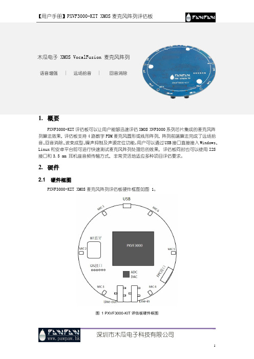
木瓜电子 XMOS VocalFusion 麦克风阵列语音增强 | 远场拾音 | 回音消除1.概要PXVF3000-KIT评估板可以让用户能够迅速评估XMOS XVF3000系列芯片集成的麦克风阵列算法效果,评估板支持4路数字PDM麦克风圆形或线形阵列,阵列前端算法完成了远场拾音、回音消除、波束成型、噪声抑制及声源定位功能。
用户可以通过USB接口直接接入Windows、Linux和安卓平台即可进行快速测试麦克风阵列处理后的效果,评估板同时也可以使用I2S 接口和3.5 mm 耳机座音频传输方式,非常灵活地适应多种项目评估要求。
2.硬件2.1 硬件框图PXVF3000-KIT XMOS麦克风阵列评估板硬件框图如图 1。
图 1 PXVF3000-KIT评估板硬件框图硬件框图包含如下内容:USB:♦USB提供设备5V电源供应♦USB Audio Class 2.0/1.0(UAC 2.0/ UAC 1.0)传输音频信号♦USB DFU PXVF3000-KIT评估板固件更新♦USB HID 指令/控制传输MIC:♦Invensence ICS-41350 PDM 麦克风♦MIC 1~6 圆形均匀分布,半径43mmPXVF3000:♦核心板,完成远程拾音、回音消除、波束成型等语音前端算法硬件模组BT蓝牙:蓝牙模块将PXVF3000的输入输出音频信号无线传输ADC/DAC:♦DAC负责PXVF3000的数字转模拟信号播放输出♦ADC可以使用模拟信号转换数字信号输入,作为PXVF3000的回音消除参考信号FPC接口:实现线形(长条形)麦克风阵列扩展,其他麦克风阵列阵型调整性扩展I2S接口:I2S数据接口兼容主从模式输入输出PXVF3000声音信号Line-out:3.5mm耳机座子立体声输出PXVF3000声音信号Line-in:3.5mm耳机座子Mono通道输入给PXVF3000作为参考信号3.评估板快速使用PXVF3000-KIT评估板出厂默认使用圆形4路麦克风阵列,分别是使用MIC 1、MIC 3、MIC 4和MIC6组成的矩形阵列如图 2。
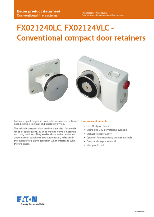
易隆电子产品数据手册说明书
©February 2021T echnical specificationCatalogue numbersDimensionsInstallation 1.Door retainer unit and striker plate should be fixed to a smooth surface.2.16mm & 20mm cable entry facilities are provided at the top and both sides.3.10mm cable entry is provided at the rear4.Fixings should be able to support at least double the holding force of the magnet.Standard connections WARNING:Do NOT use high voltage testers if ANY equipment isconnected to the system.INPUT VOLTAGETO DOOR RETAINERDescription H (mm)W (mm) D (mm)Magnet 7110844Striker Plate 656548Description CodeMains powered compact door retainer FX021240LC24V dc compact door retainer FX02124VLCFloor mounting bracket for compact door retainers FX021LCFBWWD D HHSystem functionality 1.Designed to operate only with self closing doors.2.Door retainer is fitted to wall or floor using floor bracket.3.Striker plate is fitted to door.4.Door retainer is fed with a constant supply via an external control device.5.Supply energises an electromagnet, which holds the striker plate securely against the magnet.6.If supply to magnet is interrupted, magnet will de-energise.7.Door closes under control of its own self closing device.Code FX021240LC FX02124VLCDescription Mains powered compact door retainer 24V dc powered compact door retainer SpecificationOperating voltage 230 V ac to 240 V ac 24V dcPower consumption 1.2 VA 40mAHolding force 45kg +/- 15% 50kg +/- 15%EnvironmentalOperating temperature -5°C to +40°C -5°C to +40°CHumidity (non condensing) 0 to 93 %RH 0 to 93 %RHPhysicalConstruction PC/ABS PC/ABSColour White WhiteDimensions (H x W x D) Magnet Striker plate 71mm x 108mm 44mm 65mm x 65mm x 48mm 71mm x 108mm 44mm 65mm x 65mm x 48mmWeight 0.560k g Ingress protection IP42 IP 40CompatibilitySuitable for use with Eaton conventional fire systems Eaton conventional fire systems Eaton product datasheetDoor retainers for conventional fire systems0.560k g。
1002FX_1202FX_M_CN
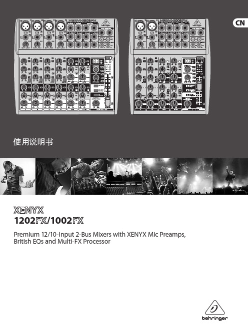
3 XENYX 1202FX/1002FX 使用说明书
重要的安全须知
带有此标志的终端设备具有强 大的电流, 存在触电危险。 仅限 使用带有 ¼'' TS 或扭锁式插头 的高品质专业扬声器线。 所有的安装或调 整均须由合格的专业人员进行。
此标志提醒您, 产品内存在未 绝缘的危险电压, 有触电危险。
此标志提醒您查阅所附的重要 的使用及维修说明。 请阅读有 关手册。 小心 为避免触电危险, 请勿打开机 顶盖 (或背面挡板)。 设备内没 有可供用户维修使用的部件。 请将维修事 项交由合格的专业人员进行。 小心 为避免着火或触电危险, 请勿 将此设备置于雨淋或潮湿中。 此设备也不可受液体滴溅, 盛有液体的容 器也不可置于其上, 如花瓶等。 小心 维修说明仅是给合格的专业维 修人员使用的。 为避免触电危 险, 除了使用说明书提到的以外, 请勿进行 任何其它维修。 所有维修均须由合格的专 业人员进行。
1. 请阅读这些说明。 2. 请妥善保存这些说明。 3. 请注意所有的警示。 4. 请遵守所有的说明。 5. 请勿在靠近水的地方使用本产品。 6. 请用干布清洁本产品。 7. 请勿堵塞通风口。 安装本产品时请遵 照厂家的说明。 8. 请勿将本产品安装在热源附近, 如暖气片, 炉子或其它产生热量的设备 ( 包 括功放器)。 9. 请勿移除极性插头或接地插头的安全 装置。 接地插头是由两个插塞接点及一个 接地头构成。 若随货提供的插头不适合您 的插座, 请找电工更换一个合适的插座。 10. 妥善保护电源线, 使其不被践踏或刺 破, 尤其注意电源插头、多用途插座及设备 连接处。
1.3.1 发货.............................................................................................. 4 1.3.2 开始使用.................................................................................... 4 1.3.3 网上登记.................................................................................... 5 2. 操...................................................................................................... 5 2.1 单声通道............................................................................................ 5 2.2 立体声通道...................................................................................... 6 2.3 主控部分的连接区........................................................................ 6 2.4 主控部分........................................................................................... 7 2.5 数字效果处理器............................................................................ 7 3. 应用.................................................................................................. 8 3.1 录音工作室........................................................................................ 8 3.2 现场放音........................................................................................... 9 4. 安装................................................................................................10 4.1 电源连接..........................................................................................10 4.2 音频连接.........................................................................................10 5. 技术参数.......................................................................................11
捷麦 CW10 型 WiFi 模块用户手册说明书
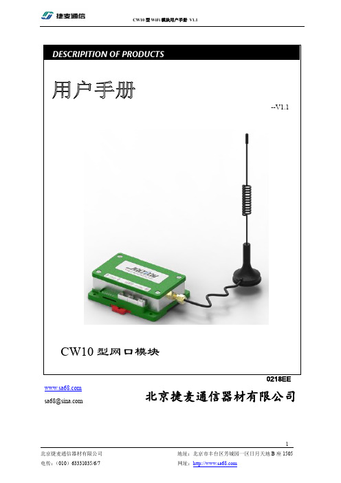
--V1.1CW10型网口模块 DESCRIPITION OF PRODUCTS北京捷麦通信器材有限公司 *************版权声明北京捷麦通信器材有限公司版权所有,并保留对本手册及本声明的最终解释权和修改权。
本手册的版权归北京捷麦通信器材有限公司所有。
未得到北京捷麦通信器材有限公司的书面许可,任何人不得以任何方式或形式对本手册内的任何部分进行复制、摘录、备份、修改、传播、翻译成其它语言、将其全部或部分用于商业用途。
免责声明本手册依据现有信息制作,其内容如有更改,恕不另行通知。
北京捷麦通信器材有限公司在编写该手册的时候已尽最大努力保证其内容准确可靠,但不对本手册中的遗漏、不准确或印刷错误导致的损失和损害承担责任。
我们会经常对手册中的数据进行检查,并在后续的版本中进行必要的更正。
欢迎您提出宝贵意见。
技术支持北京捷麦通信器材有限公司建立了以总部技术支持中心、区域技术支持中心和本地技术支持中心为主体的完善的服务体系,并提供电话热线服务。
您在产品使用过程中遇到问题时可随时与北京捷麦通信器材有限公司技术支持服务热线联系。
此外,您还可以通过北京捷麦通信器材有限公司网站及时了解最新产品动态,以及下载需要的技术文档。
北京捷麦通信器材有限公司:地址:北京市丰台区芳城园一区日月天地B座1505邮编:100017电话:************/6/7传真:************E-mail:****************网站:阅读指南手册目标通过阅读该用户手册,可以了解CW10的外观结构及安装、知道CW10如何与PC计算机连接通信、熟悉CW10的各种工作模式及其参数意义,会使用参数配置软件完成对CW10的参数操作,依据常用功能的调试流程应用CW10产品的基本功能。
使得用户完全能够应用本产品所提供的所有功能。
阅读对象本手册为具有一定工控背景知识的工程人员、安装人员及电气人员编写,其内容涵盖了CW10的安装、功能模式讲解和调试等信息。
蜂巢系列面板总线输入输出模块用户数据说明书
Panel Bus I/O ModulesProduct DataCopyright © 2016 Honeywell GmbH ● All Rights ReservedEN0Z-0979GE51 R03163.4GENERALThe CentraLine Panel Bus I/O Modules communicate via the Panel Bus.The pluggable CentraLine Panel Bus I/O modules consist of a terminal socket and a removable electronic module, allowing the socket to be mounted and wired before the electronic module is installed. All such electronic modules can be swapped out without disrupting the power and bus connec-tions: Simply unplug the “old” and insert the “new” module.Risk of electric shock or equipment damage!► Do not touch any live parts in the cabinet.► Disconnect the power supply before you start to installthe control system. More than one disconnect switch may be required to de-energize the system.► Do not reconnect the power supply until you havecompleted the installation.► Unused terminals must be closed (by completelyscrewing in the terminal screws), thus preventing the accidental touching of “live” parts.The mixed CentraLine Panel Bus I/O modules offer a mix of 34 inputs and outputs in a compact housing.Software updates, configuration, and commissioning are all done automatically by the controller for all Panel Bus I/O Modules.The Panel Bus I/O Modules are addressed manually by adjusting their HEX switches.The Panel Bus I/O Modules may be used with any CPU supporting Panel Bus communication (e.g., the LION, EAGLE, etc.).FEATURES∙ Plug-and-play functionality for easy maintenance. ∙ Pluggable Panel Bus I/O modules can be exchanged without rewiring. Further, the separate installation of terminal sockets and electronic modules lower risk of damage and theft in the construction phase.∙ Fast wiring with state-of-the-art push-in terminals (screw-type terminals also available) and bridge connectors. ∙ Wide range of sensors supported (NTC20k Ω, NTC10k Ω, PT1000-1/-2, Johnson A99 PTC, NI1000TK5000, PT3000, Balco500, 0/2…10 V, 0/4…20 mA). NOTE : The mixed Panel Bus I/O modules CLIOP830 and CLIOP831 feature inputs suitable for signals from NTC20k Ω sensors and 0/2…10 V, 0/4…20 mA, only!∙ Binary input LEDs of the pluggable CentraLine Panel Bus I/O Modules can be configured for status display (off / yellow) or alarm display (green / red) per channel. NOTE : The mixed I/O modules CLIOP830 and CLIOP831 feature only non-configurable binary input LEDs!∙ Configurable safety position for outputs, in case of loss of communication with the controller.∙ Max. wiring flexibility due to optional accessories like auxiliary terminals, manual disconnectors, and cross-connectors.∙ Can be mounted in small installation housings∙ Flexible mix of Panel Bus I/O modules covering all your application requirements.PANEL BUS I/O MODULES – PRODUCT DATAEN0Z-0979GE51 R0316 2CLIOP821ACLIOP822A CLIOPR822A CLIOP823A CLIOP824A CLIOPR824A CLIOPR825ACLIOP830AXS821-22XSU821-22CONTROLLERXS823XSU823XS824-25XSU824-25(with integrated socket)Panel BusCLIOP831AFig. 1. Overview of CentraLine Panel Bus I/O ModulesTable 1. Overview of CentraLine Panel Bus I/O Modulesorder number description Pluggable Panel Bus I/O ModulesCLIOP821 Pluggable Panel Bus Analog Input Module (with 8 analog inputs) CLIOP822 Pluggable Panel Bus Analog Output Module (with 8 analog outputs)CLIOPR822 Pluggable Panel Bus Analog Output Module (with 8 analog outputs and manual overrides) CLIOP823 Pluggable Panel Bus Binary Input Module (with 12 binary inputs) CLIOP824 Pluggable Panel Bus Relay Output Module (with 6 relay outputs)CLIOPR824 Pluggable Panel Bus Relay Output Module (with 6 relay outputs and manual overrides)CLIOPR825 Pluggable Panel Bus Floating Output Module (with 3 floating outputs and manual overrides)Mixed Panel Bus I/O Modules with integrated socketCLIOP830 Mixed Panel Bus I/O Module (with 8 AIs, 8 AOs, 12 BIs, and 6 ROs); housing fits to LION Controller housing CLIOP831 Mixed Panel Bus I/O Module (with 8 AIs, 8 AOs, 12 BIs, and 6 ROs); housing fits to EAGLE Controller housing Terminal Sockets (not needed for the mixed I/O modules CLIOP830 and CLIOP831)XS821-22 Push-in terminal socket for pluggable AI/AO modules (incl. bridge connector, swivel label) XSU821-22 Screw-type terminal socket for pluggable AI/AO modules (incl. bridge connector, swivel label) XS823 Push-in terminal socket for pluggable BI modules (incl. bridge connector, swivel label) XSU823 Screw-type terminal socket for pluggable BI modules (incl. bridge connector, swivel label)XS824-25 Push-in terminal socket for pluggable relay/floating output modules (incl. bridge connector, cross connector, swivel label)XSU824-25Screw-type terminal socket for pluggable relay/floating output modules (incl. bridge connector, cross connector, swivel label)PANEL BUS I/O MODULES – PRODUCT DATAEN0Z-0979GE51 R03163XS812XS812ROXS814XS830XS816XAL10XAL11NOTE: All CentraLine Panel Bus I/O Modules are protected against short circuit, 24 VAC +20% and 30 VDCPANEL BUS I/O MODULES – PRODUCT DATAEN0Z-0979GE51 R0316 4Table 3. Pluggable Panel Bus I/O Module specificationsModuleAnalog InputAnalog OutputBinary Input Relay OutputFloating Output CLIOP821CLIOP822, CLIOPR822CLIOP823CLIOP824, CLIOPR824CLIOPR825no. of I/Os 8 analog inputs8 analog outputs12 binary inputs requiring a gold contact or open collector6 relay outputs3 floating outputscharac-teristicLinear Graph, 0..10 Vdc with pull-up, 0(2)…10 Vdc without pull-up NTC20k Ω (-50…+150 °C, default)NTC10k Ω (-30…+100 °C) PT 1000-1 (-50…150 °C) PT 1000-2 (0…400 °C)Johnson A99 (-40…+120 °C) NI1000TK5000 (-30…+130 °C) PT 3000 (-50…150 °C) BALCO 500 (-30…120 °C)Also configurable as: binary inputs▪ Linear graph (0…10 V with pull-up)Features: ▪ 16-bit resolution▪ configurable offset per input ▪ auxiliary voltage: 10 Vdc, I max = 5 mA0…11 Vdc / ± 1 mA, 8-bit resolution (default) Also configurable as: floating outputs or binary outputs (0 V / 10 V)Features:▪ 8-bit resolution ▪ Safety position (remain, 0%, 50%, 100%)▪ red LED per output ▪ light intensity follows output level in autoVersion with manual override (R):▪ 1 potentiometer per output▪ auto feedback signal (mode + value) ▪ blinking in manual override positionstatic binary input, (default: dry contact)Also configurable as:totalizers (20 Hz)Features:▪ 1 LED per input ▪ Color mode can be set per input to OFF/yellow or green/red using CARE ▪ ON: < 1.6 k Ω to GND or < 2.5 V to GND,OFF: > 90 k Ω to GND or > 4 V to GNDrelay outputs (default)Features:▪ Changeover relays ▪ Voltage: 19…250 Vac, 1…29 Vdc, P>50 mW ▪ max. total current: 12 A▪ current per relay: N.O.: 4(4) A (AC) or 4(1) A (DC),N.C.: 2(1) A (AC) or 4(1) A (DC) ▪ Safety position(remain, 0%, 100%) ▪ yellow LED per outputVersion with manual override (R):▪ 1 switch per output ▪ auto feedback signal (mode + value) ▪ blinking in manual override positionfloating outputsFeatures: ▪ 2 relays per floating output ▪ Voltage:19…250 Vac, 1…29 Vdc, P>50 mW▪ max. total current: 12 A▪ current per relay: N.O.: 4(4) A (AC) or 4(1) A (DC), N.C.: 2(1) A (AC) or 4(1) A (DC)▪ 1 potentiometer per floating output▪ 2 LEDs per output: green: relay 1closed, red: relay 2 closed▪ blinking in manual override position ▪ auto feedback signal (mode + value)Manual Overrides as per EN ISO 16484-2:2004The manual override switches and potentiometers of the output modules (…R822, …R824, and CLIOPR825) support direct operation as per EN ISO 16484-2:2004, section 5.4.3 "Local Priority Override/Indicating Units."Specifically, the positions of the manual override switches and potentiometers directly control the outputs – independently of the controller and HMI. When a manual override switch or potentiometer is not in its default position ("auto"), the corresponding output LED will blink continuously, and the output module will send a feedback signal with the status"manual override" and the given override position to the controller (which will then also store this information in its alarm memory).NOTE: When updating the firmware of output modules, their outputs are turned OFF – regardless of the position of theirmanual override switches and/or potentiometers.Table 4. Mixed CentraLine Panel Bus I/O module specifications (CLIOP830 and CLIOP831)Analog InputsAnalog OutputsBinary InputsRelay OutputsNumber: 8Configurable types:▪ NTC20k Ω (-30…+110 °C) (default)▪ Linear Graph▪ 0..10 Vdc with pull-up▪ 0(2)…10 Vdc without pull-upAlso configurable as: ▪ binary inputs (static, dry contact, only)Features:▪ 10-bit resolution▪ configurable offset per inputNumber: 8Configurable types:▪ 0…11 Vdc / ± 1 mA (default)Also configurable as:▪ binary outputs (0 V / 10 V)Features:▪ 10-bit resolution (default) ▪ Safety position (remain, 0%, 50%, 100%)Number: 12 (requiring a gold contact or open collector)Configurable types:▪ Static binary inputs (default: static, dry contact)▪ ON: < 1.6 k Ω to GND or < 2.5 V to GND,OFF: > 90 k Ω to GND or > 4 V to GNDAlso configurable as: ▪ totalizers (15 Hz)Features:▪ 1 yellow LED per inputNumber: 6Configurable types: ▪ Relay outputs (default)Features:▪ Voltage: 24 VAC/DC, P>50 mW▪ max. total current: 3 A (AC/DC)▪ current per relay: 500 mA ▪ normally-open contacts: P > 50 mW, voltage: 24 V (AC/DC)▪ 1 yellow LED per outputPANEL BUS I/O MODULES – PRODUCT DATAEN0Z-0979GE51 R03165Legend1 Controller (e.g., LION, EAGLE, HAWK, etc.)2 Cable (power, Panel Bus) connection from controller toPanel Bus I/O Modules 3 Swivel label holder4 Cable connection between Panel Bus I/O Modules onseparate DIN rails5 Bridge connectors between Panel Bus I/O Modules onsame DIN rail 6 Stopper (from 3rd -party supplier) 7 Auxiliary terminal packagesLEDsEach CentraLine Panel Bus I/O Module is equipped with: ∙ one green power LED ∙ one yellow service LEDOvervoltage ProtectionAll inputs and outputs are protected against 24 Vac and 40 Vdc overvoltage as well as against short-circuiting.Service LEDEach Panel Bus I/O Module is equipped with a yellow service LED (status: yellow/OFF) for easy diagnosis of failures.MicroprocessorEach Panel Bus I/O Module is equipped with its own microprocessor.AddressingAddressing is performed using the HEX switch.System ConstraintsTable 5. System constraintsMax. no. of I/O modules (any combination) per controller depends uponcontroller type Max. no. of I/O modules per row 10 Max. current (F1) 4 A Max. current (F2) 12 A Max. current (F3)12 A Max. current (F4) (mixed I/Omodules, only) 3 A Max. row length3 m Max. distance between rows 40 m Min. cross-section of GND (terminal 9) (protected by F2) 1.5 mm 2PANEL BUS I/O MODULES – PRODUCT DATAEN0Z-0979GE51 R0316 6123Fig. 3. CLIOP821 Panel Bus AI Module (shown withterminal socket)Legend1 Hex switch S2 2 Service LED3 Power LEDThe pluggable CentraLine Panel Bus Analog Input Module, with 8 analog inputs, is installed with the XS821-22 or XSU821-22 Terminal Socket.Accessory disconnector module: XS812 (see also Table 2 on page 3).24.9 kOHMRTD10 VDCAIGNDFig. 4. Analog input low impedance (input circuit for PT1000, Johnson A99 PTC, Balco500, PT3000,NI1000TK5000, slow binary input)voltage input for active sensors)NTC10k Ω, NTC20k Ω, wall module setpoint)(schematic)Features∙ 0…10 Vdc, 2…10 Vdc without pull-up∙ 0…10 Vdc with pull-up (linear graph, e.g. used for wallmodule connection)∙ 0/4…20 mA, needs 499 Ω resistor in parallel ∙ NTC20k Ω (-50…+150 °C, default) ∙ NTC10k Ω (-30…+100 °C) ∙ PT1000-1 (-50…+150 °C) ∙ PT1000-2 (0…+400 °C)∙ NI1000TK5000 (-30…+130 °C) ∙ PT3000 (-50…+150 °C) ∙ BALCO500 (-30…+120 °C) ∙ Binary input ∙ 16-bit resolution∙ Configurable offset per input∙ Auxiliary voltage: 10 Vdc, I MAX = 5 mA ∙ Sensor failure detectionSee also section "Sensor Characteristics" on pg. 24.PANEL BUS I/O MODULES – PRODUCT DATAEN0Z-0979GE51 R03167PANEL BUS I/O MODULES – PRODUCT DATAEN0Z-0979GE51 R0316 8PANEL BUS I/O MODULES – PRODUCT DATAEN0Z-0979GE51 R031694531Fig. 10. CLIOPR822 Panel Bus AO Module (shown withterminal socket)Legend1 Hex switch S2 2 Manual overrides3 Status LEDs4 Service LED5 Power LEDThe pluggable CentraLine Panel Bus Analog Output Modules, with 8 analog outputs, are available in the following models: ∙ CLIOP822 Panel Bus Analog Output Module (withoutmanual overrides)∙ CLIOPR822 Panel Bus Analog Output Module (withmanual overrides)They are installed with the XS821-22 or XSU821-22 Terminal Socket.Accessory disconnector module: XS812 (see also Table 2 on page 3).(schematic)Features∙ 0…11 Vdc, +/-1 mA∙ Floating actuator (requires MCD3) ∙ Binary output (0 V / 10 V)∙ red LED per output (brightness according to signal level) ∙Optional versions with manual override potentiometers (Auto, 0…100%; LED flashes in override mode) ∙ Feedback on manual override signal ∙ 8-bit resolution∙ Configurable safety position for outputs in case ofcommunication problems (remain, 0%, 50%, 100%)PANEL BUS I/O MODULES – PRODUCT DATAEN0Z-0979GE51 R0316 10∙The relay module facilitates the control of peripheral devices with high load via the analog outputs.∙Input terminal 17 of MCD3 controls changeover contact K3.∙Relay terminal 18 of MCD3 controls the N.O. contacts (floating outputs) K1, K2.EN0Z-0979GE51 R031611The relay module facilitates the control of peripheral devices with high load via the analog outputs. ∙Input terminal 16 of MCE3 controls the N.O. contact K3.∙Input terminal 17 of MCE3 controls the changeover contact K2.∙Input terminal 18 of MCE3 controls the changeover contact K1.EN0Z-0979GE51 R0316 123421Fig. 15. CLIOP823 Panel Bus BI Module (shown withXS823 terminal socket)Legend1 Hex switch S22 Status LEDs3 Service LED4 Power LEDThe pluggable CentraLine Panel Bus Binary Input Module,with 12 binary inputs, is installed with the XS823 or XSU823Terminal Socket.Accessory disconnector module: XS812 (see also Table 2 onpage 3).(schematic)Features∙Static binary input (dry contact)∙Totalizer for up to 20 Hz∙LEDs per binary input supporting alarm display mode(red/green) or status mode (off/yellow).∙Color mode of each LED can be set to OFF/yellow orgreen/red in CARE.EN0Z-0979GE51 R031613EN0Z-0979GE51 R0316 141453Fig. 19. CLIOPR824 Panel Bus Relay Output Module(shown with terminal socket)Legend1 Hex switch S22 Manual overrides3 Status LEDs4 Service LED5 Power LEDThe pluggable CentraLine Panel Bus Relay Output Modules, with 6 relay outputs, are available in the following versions:∙CLIOP824 Panel Bus Relay Output Module (without manual overrides)∙CLIOPR824 Panel Bus Relay Output Module (with manual overrides)They are installed with the XS824-25 or XSU824-25 Terminal Socket.Accessory disconnector module: XS812-RO (see also Table 2 on page 3).(schematic)Features- Cross-Connecter- 1 yellow LED per output- Optional versions with manual override switches (Auto, 0, 1; LED flashes in override mode)- Feedback on manual override signal- Configurable safety position for outputs in case of communications problems (remain, OFF, ON) - Permissible Load per Relay Output Module (Total) ∙Max. load (fuse F3):19…250 Vac: 12 A1…24 Vdc: 12 A resistive, 3 A inductive- Permissible Load per Normally-Open Contact:∙Max. load:19…250 Vac: 4 A resistive or inductive1…24 Vdc: 4 A resistive, 1 A inductive∙Min. load:P > 50 mW- Permissible Load per Normally-Closed Contact:∙Max. load:19…250 Vac: 2 A resistive, 1 A inductive1…24 Vdc: 2 A resistive, 1 A inductive∙Min. load:P > 50 mWEN0Z-0979GE51 R0316 15EN0Z-0979GE51 R0316 16EN0Z-0979GE51 R031617EN0Z-0979GE51 R0316 184531Fig. 23. CLIOPR825 Panel Bus Floating Output Module(shown with terminal socket)Legend1 Hex switch S2 2 Manual overrides3 Status LEDs4 Service LED5 Power LEDThe pluggable CLIOPR825 Panel Bus Floating Output Module, with manual overrides and 3 floating outputs, is installed with the XS824-25 or XSU824-25 Terminal Socket. Accessory disconnector module: XS812-RO (see also Table 2 on page 3).(schematic)Features- Cross-Connecter- 1 red LED (opening) and 1 green LED (closing) perfloating output- Manual override potentiometers (Auto, 0%...100%; LEDflashes in override mode)- Feedback on manual override signal- Configurable safety position for outputs in case ofcommunication problems (remain, 0%, 50%, 100%) - Permissible Load per Floating Output Module (Total)∙ Max. load (fuse F3):19…250 Vac: 12 A1…24 Vdc: 12 A resistive, 3 A inductive- Permissible Load per Normally-Open Contact:∙ Max. load:19…250 Vac: 4 A resistive or inductive 1…24 Vdc: 4 A resistive, 1 A inductive ∙ Min. load: P > 50 mW- Permissible Load per Normally-Closed Contact:∙ Max. load:19…250 Vac: 2 A resistive, 1 A inductive 1…24 Vdc: 2 A resistive, 1 A inductive ∙ Min. load: P > 50 mWEN0Z-0979GE51 R031619EN0Z-0979GE51 R031620Mixed I/O ModulesCLIOP830CLIOP831Fig. 26. Mixed Panel Bus ModulesThe CLIOP830 and CLIOP831 mixed Panel Bus I/O modules feature 8 analog inputs, 8 analog outputs, 12 binary inputs, and 6 relay outputs.The CLIOP830 is equipped with push-in terminals, while the CLIOP831 features screw-type terminals.Both feature an integrated terminal socket and electronic module and come complete with one bridge connector and one swivel label.The CLIOP830 can be equipped with up to two rows of (XS830 and/or XS831) auxiliary terminal blocks on the top and/or bottom.The CLIOP831 can be equipped with up to two rows of (XS830 and/or XS831) auxiliary terminal blocks on the top, only.with 4 optional aux. terminal blocks (top view)1BIwith 4 optional aux. terminal blocks (top view)Features- 1 yellow LED per output- Configurable safety position for outputs in case of com-munications problems (remain in last position, OFF, ON)Table 6. Permissible loads of Mixed Panel Bus I/OModulesmax. loadmin. load per module (total for all relaycontacts)24 VDC/VAC3 A resistive or inductive, cos φ ≥ 0.6,no capacitive load, protected by fuse F4–per nor-mally open contact24 VDC/VAC , 0.5 A resistive or inductive, cos φ ≥ 0.6, no capacitive load >50 mW, 0.05 A res./ind.,cos φ ≥ 0.6voltage input for active sensors)for NTC10k Ω, NTC20k Ω, wall module setpoint)PANEL BUS I/O MODULES – PRODUCT DATAEN0Z-0979GE51 R031621PANEL BUS I/O MODULES – PRODUCT DATAEN0Z-0979GE51 R0316 22PANEL BUS I/O MODULES – PRODUCT DATAEN0Z-0979GE51 R031623Approvals, Certifications, and StandardsApprovals and Certifications∙ CE-approved∙ Conforms to EN 60730-1 and EN 60730-2-9∙ Investigated according to United States StandardUL916 (USL-listed) as well as according to Canadian National Standard(s) C22.2 (CNL-listed)Classification according to EN60730-1Environmental conditions: For use in home (residential,commercial, and light-industrial) environmentsPollution degree: Class 2 Protection against shock: Class II Software class: Class A Overvoltage category: IIClassification according to EN60529(Degree of Protection Provided by Enclosures) Classification: IP20Ambient Environmental LimitsOperating temperature: 0 … +50 °C at 5…93% r.H. Storage temperature: -20 … +70 °C at 5…93% r.H. Humidity: 5 … 93% r.h. non-condensingCurrent Requirement and Heat DissipationThe Panel Bus I/O Modules are equipped with highly-efficient switching power supplies which provide for relatively uniform power consumption over a wide range of supply voltages (see Table 7). The specific heat dissipation inside the modules amounts to less than 2 W for all models.Table 7. Current requirements of CentraLine Panel BusI/O Modulesdevices poweredsupply voltage24 Vac 24 Vdc CLIOP821130 mA 80 mA CLIOP822, CLIOPR822 150 mA 90 mA CLIOP823, CLIOL823180 mA 130 mA CLIOP824, CLIOPR824, CLIOPR825 140 mA 80 mA CLIOP830, CLIOP831 200 mA95 mAPANEL BUS I/O MODULES – PRODUCT DATAEN0Z-0979GE51 R0316 24MechanicalHousing dimensions (H x W x D)The pluggable CentraLine I/O Modules (mounted on Terminal Sockets) all have the dimensions: 110 X 90 X 93 mm (see also Fig. 34 on page 25).The CLIOP830 mixed Panel Bus I/O module has thedimensions: 216 X 110 X 93 mm (see also Fig. 35 on page 25).The CLIOP831 mixed Panel Bus I/O module has thedimensions: 216 X 110 X 61 mm (see also Fig. 36 on page 26).Housing MaterialPlastic, flame-retardantMounting MethodsDIN-rail mounting (e.g. in control cabinet).Calculated Lifetime of Weakest ComponentsMTBF ≥ 13.7 years (under typical operating conditions)Sensor CharacteristicsThe following sensor characteristics do not include failures due to:● sensor failures;● wiring resistance or wiring failures;● misreadings due to a meter connected to measureresistance or voltage at the input.For more-detailed values, see section "Appendix 3: Sensor Characteristics" of the CentraLine I/O Modules – Installation & Commissioning Instructions (EN1Z-0973GE51).Table 8. BALCO 500Temp. [°C] Resistance [Ω] Terminal voltage [V]-20.0 415 0.164 0.0 453 0.179 20.0 493 0.194 40.0 535 0.210 60.0 579 0.227 80.0 625 0.245 100.0 673 0.263 120.0 724 0.283Table 9. NTC 20 kOhmTemp. [°C]Resistance [k Ω] Terminal voltage [V]-20.0 221.0 8.08 0.0 70.2 6.76 20.0 25.3 4.75 40.0 10.2 2.81 60.0 4.521.5180.0 2.17 0.792 100.0 1.11 0.425 120.0 0.61 0.238Table 10. Pt 1000Temp. [°C]Resistance [Ω] Terminal voltage [V]-20.0 922 0.357 0.0 1000 0.386 20.0 1078 0.415 40.0 1155 0.443 60.0 1232 0.471 80.0 1309 0.499 100.0 1385 0.527 120.0 1461 0.554Table 11. Ni1000TK5000Temp. [°C]Resistance [Ω] Terminal voltage [V]-20.0 913.5 0.354 0.0 1000.0 0.386 20.0 1090.7 0.420 40.0 1185.7 0.455 60.0 1285.4 0.491 80.0 1390.1 0.529 100.0 1500.0 0.568 120.0 1615.4 0.609Table 12. NTC 10 kOhmTemp. [°C]Resistance [k Ω] Terminal voltage [V]-20.0 97.073 7.241 0.0 32.650 5.299 20.0 12.490 3.207 40.0 5.327 1.724 60.0 2.488 0.898 80.0 1.258 0.478 100.0 0.6800.265Table 13. Pt 3000Temp. [°C]Resistance [k Ω] Terminal voltage [V]-20.0 3.090 1.104 0.0 3.266 1.160 20.0 3.440 1.214 40.0 3.613 1.267 60.0 3.784 1.319 80.0 3.954 1.370 100.0 4.122 1.420 120.0 4.2891.469PANEL BUS I/O MODULES – PRODUCT DATAEN0Z-0979GE51 R031625dimensions (in mm)PANEL BUS I/O MODULES – PRODUCT DATAManufactured for and on behalf of the Environmental & Energy Solutions Division of Honeywell Technologies Sàrl, Rolle, Z.A. La Pièce 16, Switzerland by its Authorized Representative:CentraLineHoneywell GmbH Böblinger Strasse 1771101 Schönaich, Germany Phone +49 (0) 7031 637 845 Fax +49 (0) 7031 637 740 ******************* Subject to change without notice EN0Z-0979GE51 R03161BI。
R4042 模块用户手册说明书

2005年8月北京捷麦通信器材有限公司*************目录1 概述 (4)1.1 端子分配 (5)1.2 结构图 (6)1.3 接线说明 (7)1.4 默认设置 (7)1.5 设置列表 (8)2. 指令 (9)2.1 通用指令集 (10)2.1.1 %AANNTTCCFF (11)2.1.2 $AA2 (12)2.1.3 $AA5 (13)2.1.4 $AAF (14)2.1.5 $AAM (15)2.1.6 ~AAO(数据) (16)2.2 常规指令集 (17)2.2.1 #** (18)———————————————————————————————————————————————— 北京捷麦通信器材有限公司地址:北京市丰台区菜户营东街甲88号鹏润家园静苑B座2504 电传:(010)63331035--37网址:12.2.2 $AA4 (19)2.2.3 #AABBDD (20)2.2.4 $AA6 (22)2.2.5 @AA(数据) (23)2.2.6 @AA (24)2.3 主看门狗指令集 (25)2.3.1 ~** (25)2.3.2 ~AA0 (26)2.3.3 ~AA1 (27)2.3.4 ~AA2 (28)2.3.5 ~AA3EVV (29)2.3.6 ~AA4V (31)2.3.7 ~AA5V (33)3. 应用注意 (35)3.1 INIT*端子操作 (35)3.2 模块状态 (35)3.3 双重看门狗操作 (36)3.4 复位状态 (36)———————————————————————————————————————————————— 北京捷麦通信器材有限公司地址:北京市丰台区菜户营东街甲88号鹏润家园静苑B座2504 电传:(010)63331035--37网址:23.5 数字输出 (37)3.6 锁存数字输入 (37)附录:(指令集) (39)———————————————————————————————————————————————— 北京捷麦通信器材有限公司地址:北京市丰台区菜户营东街甲88号鹏润家园静苑B座2504 电传:(010)63331035--37网址:3———————————————————————————————————————————————— 北京捷麦通信器材有限公司 地址:北京市丰台区菜户营东街甲88号鹏润家园静苑B 座2504 电传:(010)63331035--37 网址:41 概述R4000 是具有网络数据采集和控制功能的一系列模块。
科大讯飞阵列麦克风硬件设计方案

科大讯飞转接板硬件方案一、概述1.1方案应用场合该转接板主要用于金融自助产品线的部分需要语音识别等录入音质要求比较高的产品中。
1.2实现的主要功能实现语音唤醒,对唤醒方位音频进行增强,同时降低其他角度的声音强度和对功放放出的声音进行采样通过内置算法尽量消除白噪声,达到在较嘈杂的环境仍有较好的音频质量的效果。
1.3方案概述该方案为科大讯飞核心板的转接板,主要由音频输出电路、回声输入电路、串口电路、电源电路按键电路等部分组成1.3.1音频输出电路:核心板的HPL/HPR音频输出峰峰值在500mv左右,普通电脑MIC IN接口能够接受输入音频最大峰峰一般为50mv左右,为避免音频输出到主机MIC IN的波形被削波。
采用核心板数据手册推荐分压电路对输出音频进行分压处理。
数据手册推荐音频分压输出电路如下:V(HPR)=500mv V(mic+)=50 R1=10K 计算得:R2=1.1K考虑到计算MIC IN电路存在不同,尽量减小削波的可能,提高兼容性,此处将R2调整为470欧姆,话筒输入声音增益可以通过电脑控制面板对输入声音增益进行调整。
原理图中MIC的音频输出部分电路图:1.3.2回音输入:回音输入电路采用数据手册中的差分方式输入,我司在金融自助产品线上使用的喇叭多为8Ω5W,由功率和阻抗算得其工作时有效电压值U=(P/R)0.5(算式来源P=U2/R)算得最大功率下电压的有效值在6.3V左右,了解得知我司在金融自助产品线上的功放多为D类功放,D类功为推完输出末端为推挽方式,该方式输出加到喇叭上电压的最大值一般为电源电压12/24V,在加上喇叭属于感性负载,考虑到设计余量,此处取最大电源电压24V的1.5倍36V作为喇叭上可能存在的最大峰峰值带入公式计算。
R3=10K R5=10K V(OUT+)-V(OUT-)=36V参考信号输入最大电压[V(REF+)-V(REF-)]max=150mV计算得R4=0.083K 考虑到输入信号需要过1uf隔直电容,手册中推荐的R3,R5的阻值较大,且产品的喇叭输出音量应该不会达到100%音量状态,此处R4暂采用200欧姆电阻。
HFM1202 Ethernet Receiver 数据手册说明书
Ethernet ReceiverOUTLINE DIMENSIONS in inches (mm)DESCRIPTIONFEATURES-35 dBm to -12 dBm sensitivity •Differential data outputs (ECL compatible)•Signal Quality Detect and Packet Detect outputs (open collector)•Adjustable signal quality detect level •ST¨ interface•500 í output drive capability•Monolithic design - less board space, high reliability•The HFM1202-331 Ethernet fiber optic receiver module is designed for use in computer LAN (10 Mb/s Ethernet) applications. The 9 pin Next Generation module is intended for use in applications such as IEEE 802.3 10 BASE FB/FL and FOIRL signal standards. A PIN photodiode plus pre-amp is mounted in the fiber optic connector for maximum shielding, and providesamplification and current-to-voltage conversion. The post-amp IC provides final amplification to the logic output levels (see BLOCK DIAGRAM). Signal Quality Detect, Packet Detect and Differential Data outputs are available. Differential ECL compatible data minimizes pulse width distortion and allows capacitive coupling to ECL logic. The HFM1202 has a 500 ½ output drive capability on each data output. An internally regulated power supply increases power supply rejection.Case ground is separated from circuit ground, allowing feedthrough mounting of the barrel.APPLICATIONAverage-to-peak input level monitoring aids in the generation of the signal quality logic signal (Ç) when the input level is adequate for 10øÀÉ BER. The open collector output timing response of Ç is intended to meet 802.3 requirements over -32.5 dBm to -12 dBmaverage power levels. An additional current source output (SQLED) is available to drive an external LED indicator (LED ON indicates poor signal quality). If this output isnot used, it should be tied to +12 V.Ethernet ReceiverAPPLICATION (continued)Resistor Rà°¤ adjusts the Ç threshold upward. A 70 µAcurrent from this node to ground increases the thresholdby 1 dB of optical power. Rà°¤'s high side is at 4.3 V(nominal).The open collector output (¿) indicates presence of avalid Ethernet packet. This output goes low following thefirst two data edges that are 200 ns or less apart at thestart of a packet. It returns high before the end of thefirst cycle of a valid 1 MHz idle signal.The HFM1202 is designed to operate with a 12 V supply(normally present in FOIRL interfaces and personalcomputer backplanes). The module requires a minimum+8.5 V total voltage. If a +12 V supply is not available,+5 V to VÙÙ pin and -5 V to GND pin will operate themodule. Since the outputs are typically AC coupled, thisvoltage shift is generally not a problem. Data out2 (+) ispositive with respect to data out1 (-) when no light ispresent at the optical input.ST is a registered trademark of AT & T.Honeywell reserves the right to make 560hchanges in order to improve design andsupply the best products possible.Ethernet ReceiverABSOLUTE MAXIMUM RATINGS(25¡C Free-Air Temperature unless otherwise noted)8.5 to 15.75 V Supply voltage (VÙÙ)-40 to +85¡CTemperatureStresses greater than those listed under "Absolute Maximum Ratings" may cause permanent damage to the device. This is a stress rating only and functional operation of the device at these or any other conditions above those indicated in the operational section of this specification is not implied. Exposure to absolute maximum rating conditions for extended periods of time may affect reliability.ELECTRO-OPTICAL CHARACTERISTICS (Over 0 to 70¡C, VÙÙ = 11.25 to 15.75 VDC unless otherwise stated)UNITS TEST CONDITIONS MIN PARAMETERSYMBOLTYP MAXManchester coding Data RateMbd 10Average power (10øÀÉ BER)Input Power dBm -35-12Excluding Ç, SQLED, ¿Supply Current mA 3243Propagation Delay ns 2840RMS, -32.5 dBm average input Jitter (uncorrelated)ns 0.40.6Ç Low, -12 dBm averagePulse Width Distortion [À] ns 7inputThreshold for Ç, high to lowSignal Quality Detect (Ç) [Á] dBm -35-32.5Transitionaverage Threshold change for ÇSignal Quality Detect Hysteresis dB -1.3low to high transition PÛÜ > -30 dBm average Delay Time (acceptable level) [Â] µs 4PÛÜ < -12 dBm average Delay Time (unacceptable level)µs320Bit times @ 10 Mbd (with Packet Detection (¿) < 20 p¸ and 4 kí load)Delay of Packet Start 2End of Packet Delay 4Optical Idle Signal PKT DE assertionFrequency MHz 0.8511.25Duty Cycle%4555Output (Out1/Out2)Loadí500Peak to peak Output Swing V 11.6Over temperatureppm/¡C +1000IÞÚ – 3 mA¾ VÞÚV 0.4SQLED Sink CurrentmA12Notes1. Using a 10 MHz square wave input optical signal; t²= 7 ns, t¶= 10 ns. The maximum PWD specified could be achieved by the user in system operation at 70¡C.2. Using Rà°¤ = infinity Ohms.3. See Figure 1.RECOMMENDED OPERATING CONDITIONS Supply voltage (VÙÙ)11.25 to 12.75 V Temperature 0 to +70¡CDescriptionCatalog Listing ORDER GUIDE HFM1202-331Fiber Optic Ethernet Receiver, 9 pin package The inherent design of this component causes it to be sensitive to electrostatic discharge (ESD). To prevent ESD-induced damageand/or degradation to equipment, take normal ESD precautions when handling this product.CAUTIONHoneywell reserves the right to make changes in order to improve design and supply the best products possible.h561Ethernet ReceiverBLOCK DIAGRAMFIBER009.SCHSQ Transition Delay vs PowerFig. 1FIBER073.GRA。
麦克风阵列模块XFM10412数据手册
7.2.3 指定增强波束 ............................................................................................................................... 9
8 I2C 通讯接口......................................................................................................................................9
8.7.1 协议介绍 .....................................................................................................................................14
8.7.2 参考示例 .....................................................................................................................................14
一种分布式双麦克风线阵声源定位方法
一种分布式双麦克风线阵声源定位方法
李林剑;陈华伟
【期刊名称】《应用声学》
【年(卷),期】2014(0)5
【摘要】分布式麦克风阵列由于比传统的单阵列具有更大的空间孔径,可以获得更好的声源定位性能,因此基于分布式麦克风阵列的声源定位方法成为当前麦克风阵列领域研究的热点之一.本文研究了一种基于分布式双麦克风线阵的声源定位方法,并进行了系统实现,从理论上剖析了该算法的定位精度与单阵列定向误差以及声源位置之间的关系,而且还揭示了声源高度扰动对该算法定位精度的影响.最后,分别通过仿真实验和实际定位系统的测试结果,验证了本文理论分析的正确性.
【总页数】7页(P412-418)
【作者】李林剑;陈华伟
【作者单位】南京航空航天大学电子信息工程学院南京210016;南京航空航天大学电子信息工程学院南京210016
【正文语种】中文
【中图分类】TTN912
【相关文献】
1.分布式麦克风阵列的声源定位 [J], 张会新;闫安斌;王昕;姜维
2.一种异步分布式麦克风阵列网络声源定位 [J], 杨博;刘志骋
3.基于分布式麦克风阵列的声源定位算法 [J], 蔡卫平;黄印君;陆泽橼
4.基于分布式压缩感知的麦克风阵列声源定位 [J], 黄惠祥; 郭秋涵; 童峰
5.基于LabVIEW的双麦克风实时声源定位系统 [J], 杨国卿;王义琳;李明汝;全星日因版权原因,仅展示原文概要,查看原文内容请购买。
- 1、下载文档前请自行甄别文档内容的完整性,平台不提供额外的编辑、内容补充、找答案等附加服务。
- 2、"仅部分预览"的文档,不可在线预览部分如存在完整性等问题,可反馈申请退款(可完整预览的文档不适用该条件!)。
- 3、如文档侵犯您的权益,请联系客服反馈,我们会尽快为您处理(人工客服工作时间:9:00-18:30)。
8.7.1 协议介绍 .....................................................................................................................................14
8.7.2 参考示例 ........................................................................................................14
7.1
扩展板串口与上位机连接方法 ...................................................................................................8
7.2
串口协议介绍 ............................................................................................................................... 8
8.1
总述............................................................................................................................................... 9
8.4
模块版本号查询 ......................................................................................................................... 11
8.4.1 协议介绍 .....................................................................................................................................11
4 模块尺寸图.........................................................................................................................................2
5 硬件接口定义 .....................................................................................................................................3
8.2
写操作......................................................................................................................................... 10
8.3
读操作......................................................................................................................................... 10
8.6.2 参考示例 .....................................................................................................................................13
8.7
设置拾音波束 ............................................................................................................................. 14
8.6
复位............................................................................................................................................. 13
8.6.1 协议介绍 .....................................................................................................................................13
麦克风阵列模块 XFM10412 数据手册
科大讯飞麦克风阵列模块 XFM10412 数据手册
科大讯飞科技股份有限公司
安徽省合肥市望江西路 666 号 国家科技创新型试点市示范区科大讯飞语音产业基地
©IFLYTEK CO.,LTD.
I
麦克风阵列模块 XFM10412 数据手册
版本 V0.1 V0.2
版本历史
日期
修改记录
2016-01-29 初稿
2016-02-24 修改模块命名、修改音频输出连接上位机的方法图
©IFLYTEK CO.,LTD.
II
麦克风阵列模块 XFM10412 数据手册
声明
本手册由科大讯飞科技股份有限公司版权所有,未经许可,任何单位和个人都不得以电子 的、机械的、磁性的、光学的、化学的、手工的等形式复制、传播、转录和保存该出版物,或 翻译成其他语言版本。一经发现,将追究其法律责任。
6.1
硬件连接参考 ............................................................................................................................... 6
6.2
音频输出信号与上位机连接方法 ...............................................................................................6
©IFLYTEK CO.,LTD.
III
麦克风阵列模块 XFM10412 数据手册
目录
1 产品概述 ............................................................................................................................................1
7.2.3 指定增强波束 ............................................................................................................................... 9
8 I2C 通讯接口......................................................................................................................................9
8.4.2 参考示例 .....................................................................................................................................12
8.5
唤醒角度查询 ............................................................................................................................. 12
2 功能描述 ............................................................................................................................................1
3 系统结构图.........................................................................................................................................1
7.2.1 查询版本号 ...................................................................................................................................8
7.2.2 复位 ...............................................................................................................................................9
8.5.1 协议介绍 .....................................................................................................................................12