(完整版)muRata电感命名规则
村田磁珠命名规则
村田磁珠命名规则
村田磁珠是一种电子元器件,由于其广泛应用于各种电子设备中,因此命名规则也非常重要。
以下是村田磁珠命名规则:
1. 型号命名规则:村田磁珠的型号由三个部分组成,分别是系列、尺寸和电感值。
例如,一个村田磁珠的型号为LBC2016T220M,
其中LBC为系列,2016为尺寸,220为电感值。
2. 系列命名规则:村田磁珠的系列分为多种类型,包括LC、LQ、LH、LX、LK等。
不同的系列代表着不同的使用场景和特点。
3. 尺寸命名规则:村田磁珠的尺寸一般由长度和宽度两个参数
来表示,单位为毫米。
例如,2016代表着长度为2.0毫米,宽度为1.6毫米。
4. 电感值命名规则:村田磁珠的电感值也是一个重要的参数,
决定着其在电路中的作用。
一般以毫亨为单位来表示,例如220代表着220毫亨的电感值。
综上所述,村田磁珠的命名规则是一个相对固定的体系,有助于人们在使用和选择村田磁珠时更加方便和准确。
- 1 -。
国内外常用电子元器件型号命名规则比如:电阻器,电容器
(5)日本松下旗下三洋电机(Panasonic)
(6)韩国三星(SAMSUNG)
(7)美国基美(KEMET)
(8)英国Syfer
(9)中国台湾国巨(YAGEO)
(10)中国台湾华新科技(WALSIN)
3.电感器
4.变压器
5.二极管
6.三极管
7.发光二极管
8.扬声器
9.电声器件
10晶闸管
11.继电器
国外:
1.国际电子联合会半导体器件命名法
国际电子联合会晶体管型号命名法的特点:
1)这种命名法被欧洲许多国家采用。因此,凡型号以两个字母开头,并且第一个字母是A,B,C,D或R的晶体管,大都是欧洲制造的产品,或是按欧洲某一厂家专利生产的产品。
2)第一个字母表示材料(A表示锗管,B表示硅管),但不表示极性(NPN型或PNP型)。
3)第二个字母表示器件的类别和主要特点。如C表示低频小功率管,D表示低频大功率管,F表示高频小功率管,L表示高频大功率管等等。若记住了这些字母的意义,不查手册也可以判断出类别。例如,BL49型,一见便知是硅大功率专用三极管。
4)第三部分表示登记顺序号。三位数字者为通用品;一个字母加两位数字者为专用品,顺序号相邻的两个型号的特性可能相差很大。例如,AC184为PNP型,而AC185则为NPN型。
8)日本通常把Pcm≥1W的管子,称做大功率管。
5)第四部分字母表示同一型号的某一参数(如hFE或NF)进行分档。
6)型号中的符号均不反映器件的极性(指NPN或PNP)。极性的确定需查阅手册或测量。
2.美国半导体器件型号命名法
美国晶体管或其它半导体器件的型号命名法较混乱。这里介绍的是美国晶体管标准型号命名法,即美国电子工业协会(EIA)规定的晶体管分立器件型号的命名法。如下表:
原来国内外常用电子元器件型号命名规则是这样的,涨知识了!

原来国内外常用电子元器件型号命名规则是这样的,涨知识了!1.电阻器举例:RJ76表示精密金属膜电阻器R——电阻器(第一部分)J——金属膜(第二部分)7——精密(第三部分)6——序号(第四部分)2.电容器国外电容器命名规则不一,国外部分知名厂家命名规则如下:•(1)日本村田(muRata)•(2)日本TDK•(3)日本京瓷(Kyocera)•(4)日本罗姆(ROHM)•(5)日本松下旗下三洋电机(Panasonic)(6)韩国三星(SAMSUNG)•(7)美国基美(KEMET)•(8)英国Syfer•(9)中国台湾国巨(YAGEO)•(10)中国台湾华新科技(WALSIN)3.电感器4.变压器5.二极管6.三极管7.发光二极管8.扬声器9.电声器件10晶闸管11.继电器国外:1.国际电子联合会半导体器件命名法国际电子联合会晶体管型号命名法的特点:•1)这种命名法被欧洲许多国家采用。
因此,凡型号以两个字母开头,并且第一个字母是A,B,C,D或R的晶体管,大都是欧洲制造的产品,或是按欧洲某一厂家专利生产的产品。
•2)第一个字母表示材料(A表示锗管,B表示硅管),但不表示极性(NPN型或PNP型)。
•3)第二个字母表示器件的类别和主要特点。
如C表示低频小功率管,D表示低频大功率管,F表示高频小功率管,L表示高频大功率管等等。
若记住了这些字母的意义,不查手册也可以判断出类别。
例如,BL49型,一见便知是硅大功率专用三极管。
•4)第三部分表示登记顺序号。
三位数字者为通用品;一个字母加两位数字者为专用品,顺序号相邻的两个型号的特性可能相差很大。
例如,AC184为PNP型,而AC185则为NPN型。
•5)第四部分字母表示同一型号的某一参数(如hFE或NF)进行分档。
•6)型号中的符号均不反映器件的极性(指NPN或PNP)。
极性的确定需查阅手册或测量。
2.美国半导体器件型号命名法美国晶体管或其它半导体器件的型号命名法较混乱。
【电容的型号命名规则】murata电容命名规则
【电容的型号命名规则】murata电容命名规则电容的型号命名:1、各国电容器的型号命名很不统一,国产电容器的命名由四部分组成:第一部分:用字母表示名称,电容器为C。
第二部分:用字母表示材料。
第三部分:用数字表示分类。
第四部分:用数字表示序号。
2、电容的标志方法:(1)直标法:用字母和数字把型号、规格直接标在外壳上。
(2)文字符号法:用数字、文字符号有规律的组合来表示容量。
文字符号表示其电容量的单位:P、N、u、m、F等。
和电阻的表示方法相同。
标称允许偏差也和电阻的表示方法相同。
小于10pF的电容,其允许偏差用字母代替:B——±0.1pF,C——±0.2pF,D——±0.5pF,F——±1pF。
(3)色标法:和电阻的表示方法相同,单位一般为pF。
小型电解电容器的耐压也有用色标法的,位置靠近正极引出线的根部,所表示的意义如下表所示:颜色黑棕红橙黄绿蓝紫灰耐压 4V 6.3V 10V 16V 25V 32V 40V 50V 63V (4)进口电容器的标志方法:进口电容器一般有6项组成。
第一项:用字母表示类别:第二项:用两位数字表示其外形、结构、封装方式、引线开始及与轴的关系。
第三项:温度补偿型电容器的温度特性,有用字母的,也有用颜色的,其意义如下表所示:序号字母颜色温度系数允许偏差字母颜色温度系数允许偏差 1 A 金+100 R 黄 -220 2 B 灰 +30 S 绿 -330 3 C 黑 0 T 蓝 -470 4 G ±30 U 紫 -750 5 H 棕 -30 ±60 V -1000 6 J ±120 W -1500 7 K ±250 X -2200 8 L 红 -80 ±500 Y -3300 9 M ±1000 Z -4700 10 N ±2500 SL +350~-1000 11 P 橙 -150 YN -800~-5800 备注:温度系数的单位10e -6/℃;允许偏差是 % 。
MURATA LQH43MN系列芯片电感(Chip Inductors)商品说明书
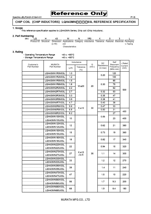
CHIP COIL (CHIP INDUCTORS )LQH43MN □□□□03L REFERENCE SPECIFICATION1. ScopeThis reference specification applies to LQH43MN Series, Chip coil (Chip Inductors).2. Part Numbering(ex) LQ H 43 M N 1R0 K 0 3 LProduct ID Structure Dimension Applications CategoryInductance Tolerance Features Electrode Packaging(L×W) a nd L:TapingCharacteristics3. Rating・Operating Temperature Range -40 to +85°C ・Storage Temperature Range-40 to +85°CCustomer’s Part Number MURATA Part NumberInductanceQ (min.)DC Resistance (Ω max) SelfResonantFrequency(MHz min)* RatedCurrent(mA)(μH)Tolerance (%)LQH43MN1R0M03L 1.0 M:±20 200.20120500LQH43MN1R2M03L 1.2 100 LQH43MN1R5M03L 1.50.3085LQH43MN1R8M03L 1.8 75LQH43MN2R2M03L 2.2 62LQH43MN2R7M03L 2.7 0.32 53 LQH43MN3R3M03L 3.3 0.35 47 LQH43MN3R9M03L 3.9 0.38 41 LQH43MN4R7K03L 4.7K:±10 300.40 38LQH43MN5R6K03L 5.6 0.47 33LQH43MN6R8K03L 6.8 0.50 31450LQH43MN8R2K03L 8.2 0.5627 LQH43MN100K03L10K:±10J:± 53523 400LQH43MN100J03LLQH43MN120K03L12 0.62 21 380LQH43MN120J03LLQH43MN150K03L15 0.73 19 360LQH43MN150J03LLQH43MN180K03L18 0.82 17 340LQH43MN180J03LLQH43MN220K03L22 0.94 15 320LQH43MN220J03LLQH43MN270K03L 27 1.1 14 300 LQH43MN270J03L LQH43MN330K03L33 1.2 12 270LQH43MN330J03LLQH43MN390K03L39 1.4 11 240LQH43MN390J03LLQH43MN470K03L47 1.5 10 220LQH43MN470J03LLQH43MN560K03L56 1.7 9.3 200LQH43MN560J03LLQH43MN680K03L68 1.9 8.4 180LQH43MN680J03LCustomer’s Part NumberMURATAPart NumberInductanceQ(min.)DCResistance(Ω max)SelfResonantFrequency(MHz min)* RatedCurrent(mA)(μH)Tolerance(%)LQH43MN820K03L82K:±10J:± 5 35 2.2 7.5 170LQH43MN820J03LLQH43MN101K03L10040 2.5 6.8 160LQH43MN101J03LLQH43MN121K03L120 3.06.2150 LQH43MN121J03LLQH43MN151K03L150 3.75.5130 LQH43MN151J03LLQH43MN181K03L180 4.55.0120 LQH43MN181J03LLQH43MN221K03L220 5.44.5110 LQH43MN221J03LLQH43MN271K03L270 6.84.0100 LQH43MN271J03LLQH43MN331K03L330 8.23.695LQH43MN331J03LLQH43MN391K03L390 9.73.390LQH43MN391J03LLQH43MN471K03L470 11.83.080LQH43MN471J03LLQH43MN561K03L560 14.52.770LQH43MN561J03LLQH43MN681K03L680 17.02.565LQH43MN681J03LLQH43MN821K03L820 20.52.260LQH43MN821J03LLQH43MN102K03L1000 25.02.050LQH43MN102J03LLQH43MN122K03L1200 30.01.845LQH43MN122J03LLQH43MN152K03L1500 37.01.640LQH43MN152J03L* When applied Rated current to the Products , self temperature rise shall be limited to 20°C max and Inductance willbe within ±10% of initial Inductance value.4. Testing Conditions<Unless otherwise specified> <In case of doubt>Temperature: Ordinary Temperature (15 to 35°C) Temperature: 20 ± 2°CHumidity: Ordinary Humidity (25 to 85 %(RH)) Humidity: 60 to 70 %(RH)AtmosphericPressure: 86 to 106 kPa5. Appearance and Dimensions■Unit Mass (Typical value)0.13g(in mm)6. Electrical PerformanceNo. Item Specification TestMethod6.1 Inductance Inductance shall meet item 3. Measuring Equipment:KEYSIGHT4192A or equivalentMeasuring Frequency:1MHz / 1.0 to 390 μH1kHz / 470 to 1500 μH6.2 Q Q shall meet item 3. Measuring Equipment:KEYSIGHT4192A or equivalentMeasuring Frequency:1MHz / 1.0 to 82 μH796kHz / 100 to 820 μH252kHz / 1000 to 1500 μH6.3 DC Resistance DC Resistance shall meet item 3. Measuring Equipment:Digital multi meter6.4 Self ResonantFrequency(S.R.F)S.R.F shall meet item 3. Measuring Equipment:KEYSIGHT E4991A or equivalent6.5 TemperatureCharacteristics Temperature Coefficient150 to 1400 PPM/°CTemperature coefficient on the basis of step 3shall meet specification after tested asfollows.It shall be subjected to the condition ofTable 1, and its inductanse shall be measuredat each step after reaching the thermalequiligrium and be calculated.Table 1Step1 / +20±2°C Step4 / +85±2°CStep2 / -25±2°C Step5 / +20±2°CStep3 / +20±2°C8. Environmental Performance (It shall be soldered on the substrate.)No. Item Specification Test Method8.1 Heat Resistance Appearance :No damageInductance Change :within ± 5% Q-factor Change :within ± 20% Temperature :85±2°CTime :1000h (+48 h, -0 h)Then measured after exposure in the room condition for 24±2 hours.8.2 Cold ResistanceTemperature :-40±2°C Time :1000h (+48 h, -0 h)Then measured after exposure in the room condition for 24±2 hours.8.3 HumidityTemperature :40±2°C Humidity :90 to 95%(RH) Time :1000h (+48 h, -0 h)Then measured after exposure in the room condition for 24±2 hours.8.4 TemperatureCycle1 cycle :step 1:-40±2°C / 30±3 minstep 2:Ordinary temp. / 10 to 15 min step 3:+85±2°C / 30±3 minstep 4:Ordinary temp. / 10 to 15 min Total of 10 cyclesThen measured after exposure in the room condition for 24±2 hours.9. Specification of Packaging(in mm)Dimension of the Cavity is measured at the bottom side.9.2 Specification of Taping(1) Packing quantity (standard quantity)500 pcs / reel (2) Packing MethodProducts shall be packed in the each embossed cavity of plastic tape and sealed by cover tape. (3) Sprocket holeThe sprocket holes are to the right as the tape is pulled toward the user. (4) Spliced pointPlastic tape and Cover tape has no spliced point. (5) Missing components numberMissing components number within 0.025 % of the number per reel or 1 pc., whichever is greater, and are not continuous. The specified quantity per reel is kept.9.3 Pull StrengthEmbossed carrier tape10N min. Cover tape5N min.2.7±0.2※The packing directions of the chip coilin taping are unified with the in/out positions of the lead wire.9.4 Peeling off force of cover tapeSpeed of Peeling off 300mm/minPeeling off force0.2 to 0.7N (minimum value is typical)9.5 Dimensions of Leader-tape, Trailer and ReelThere shall be leader-tape (cover tape) and trailer-tape (empty tape) as follows.9.6 Marking for reelCustomer part number, MURATA part number, Inspection number(*1), RoHS marking(*2), Quantity etc ・・・*1) <Expression of Inspection No.> □□ OOOO ⨯⨯⨯(1) (2) (3)(1) Factory Code(2) Date First digit : Year / Last digit of yearSeconddigit: Month / Jan. to Sep. → 1 to 9, Oct. to Dec. → O, N, DThird, Fourth digit : Day(3) Serial No.*2) « Expression of RoHS marking » ROHS – Y (△)(1)(2)(1) RoHS regulation conformity(2) MURATA classification number9.7 Marking for Outside package (corrugated paper box)Customer name, Purchasing order number, Customer part number, MURATA part number, RoHS Marking (*2) ,Quantity, etc ・・・9.8. Specification of Outer CaseOuter Case Dimensions(mm) Standard Reel Quantityin Outer Case (Reel)W D H186 186 93 4*Above Outer Case size is typical. It depends on a quantityof an order10. CautionLimitation of ApplicationsPlease contact us before using our products for the applications listed below which require especially high reliability for the prevention of defects which might directly cause damage to the third party's life, body or property.(1) Aircraft equipment(6) Transportation equipment (vehicles, trains, ships, etc.)(2) Aerospace equipment(7) Traffic signal equipment(3) Undersea equipment(8) Disaster prevention / crime prevention equipment(4) Power plant control equipment(9) Data-processing equipment(5) Medical equipment (10) Applications of similar complexity and /or reliability requirementsto the applications listed in the above165to180degreeF Cover tapePlastic tapeW DLabelHTrailer:160m in.11. NoticeThis product is designed for solder mounting.Please consult us in advance for applying other mounting method such as conductive adhesive.11.1 Land pattern designingRecommended land patterns for reflow soldering are as follows:These have been designed for Electric characteristics and solderability.Please follow the recommended patterns. Otherwise, their performance which includes electrical performance or solderability may be affected, or result to "position shift" in soldering process.Reflow Soldering(in mm)11.2 Flux, SolderFlux・Use rosin-based flux.・Don’t use highly acidic flux with halide content exceeding 0.2(wt)% (chlorine conversion value). ・Don’t use water-soluble flux.Solder・Use Sn-3.0Ag-0.5Cu solder・Standard thickness of solder paste : 200μm to 300μmOther flux (except above) Please contact us for details, then use.11.3 Soldering conditions (Reflow)・Pre-heating should be in such a way that the temperature difference between solder and product surface is limited to 150°C max. Cooling into solvent after soldering also should be in such a way that the temperature difference is limited to 100°C max.Insufficient pre-heating may cause cracks on the product, resulting in the deterioration of product quality. ・Standard soldering profile and the limit soldering profile is as follows.The excessive limit soldering conditions may cause leaching of the electrode and / or resulting in the deterioration of product quality.Reflow soldering profileStandard Profile Limit ProfilePre-heating 150~180°C 、90s ±30sHeating above 220°C 、30s ~60s above 230°C 、60s max. Peak temperature 245±3°C 260°C,10s Cycle of reflow2 times1 timeLimit ProfileStandard Profile 90s±30s 230℃260℃245℃±3℃220℃30s~60s60s max.180150Temp.(s)(℃)Time.11.4 Reworking with soldering iron.The following conditions must be strictly followed when using a soldering iron.Pre-heating 150°C,1 min Tip temperature 350°C max. Soldering iron output 80W max. Tip diameter φ3mm max. Soldering time3(+1,-0)sTimes 2 timesNote : Do not directly touch the products with the tip of the soldering iron in order to prevent the crackon the products due to the thermal shock.11.5 Solder Volume・Solder shall be used not to be exceeded the upper limits as shown below.・Accordingly increasing the solder volume, the mechanical stress to Chip is also increased. Exceeding solder volume may cause the failure of mechanical or electrical performance.1/3T ≦t ≦T (T: Lower flange thickness)11.6 Product's locationThe following shall be considered when designing and laying out P.C.B.'s.(1) P.C.B. shall be designed so that products are not subject to the mechanical stress due to warping the board.[Products direction ]Products shall be locatedin the sideways direction (Length:a<b) to the mechanical stress.(2) Components location on P.C.B. separation.It is effective to implement the following measures, to reduce stress in separating the board.It is best to implement all of the following three measures; however, implement as many measures as possible to reduce stress.Contents of MeasuresStress Level (1) Turn the mounting direction of the component parallel to the board separation surface. A > D *1 (2) Add slits in the board separation part.A >B (3) Keep the mounting position of the component away from the board separation surface.A > C*1 A > D is valid when stress is added vertically to the perforation as with Hand Separation.If a Cutting Disc is used, stress will be diagonal to the PCB, therefore A > D is invalid.(3) Mounting Components Near Screw HolesWhen a component is mounted near a screw hole, it may be affected by the board deflection that occurs during the tightening of the screw. Mount the component in a position as far away from the screw holes as possible.〈Poor example 〉〈Good example 〉ba SeamSlit ADBCb a Length:a bScrew Hole Recommended11.7 Cleaning ConditionsProducts shall be cleaned on the following conditions.(1) Cleaning temperature shall be limited to 60°C max.(40°C max for IPA.)(2) Ultrasonic cleaning shall comply with the following conditions with avoiding the resonance phenomenonat the mounted products and P.C.B.Power : 20 W /l max. Frequency : 28kHz to 40kHz Time : 5 minutes max.(3) Cleaner1. Alternative cleaner・Isopropyl alcohol (IPA)2. Aqueous agent・PINE ALPHA ST-100S(4) There shall be no residual flux and residual cleaner after cleaning.In the case of using aqueous agent, products shall be dried completely after rinse with de-ionized water in orderto remove the cleaner.(5) Other cleaningPlease contact us.11.8 Resin coatingThe inductance value may change due to high cure-stress of resin to be used for coating/molding products. Anopen circuit issue may occur by mechanical stress caused by the resin, amount/cured shape of resin, or operatingcondition etc. Some resin contains some impurities or chloride possible to generate chlorine by hydrolysis undersome operating condition may cause corrosion of wire of coil, leading to open circuit. So, please pay your carefulattention when you select resin in case of coating/molding the products with the resin. Prior to use the coatingresin, please make sure no reliability issue is observed by evaluating products mounted on your board.11.9 Caution for use・Sharp material such as a pair of tweezers or other material such as bristles of cleaning brush, shall not be touched to thewinding portion to prevent the breaking of wire.・Mechanical shock should not be applied to the products mounted on the board to prevent the breaking of the core.11.10 Handling of a substrateAfter mounting products on a substrate, do not apply any stress to the product caused by bending or twisting to the substrate when cropping the substrate, inserting and removing a connector from the substrate or tightening screw to the substrate.Excessive mechanical stress may cause cracking in the product.Bending Twisting11.11 Storage and Handling Requirements(1) Storage periodUse the products within 12 months after delivered.Solderability should be checked if this period is exceeded.(2) Storage conditions・Products should be stored in the warehouse on the following conditions.Temperature : -10 ~ 40°CHumidity : 15 to 85% relative humidity No rapid change on temperature and humidityThe electrode of the products is coated with solder. Don't keep products in corrosive gases such as sulfur,chlorine gas or acid, or it may cause oxidization of electrode, resulting in poor solderability.・Products should not be stored on bulk packaging condition to prevent the chipping of the core and the breakingof winding wire caused by the collision between the products.・Products should be stored on the palette for the prevention of the influence from humidity, dust and so on.・Products should be stored in the warehouse without heat shock, vibration, direct sunlight and so on.(3) Handling ConditionCare should be taken when transporting or handling product to avoid excessive vibration or mechanical shock. 12.Note(1) Please make sure that your product has been evaluated in view of your specifications with our product being mountedto your product.(2) You are requested not to use our product deviating from the reference specifications.(3) The contents of this reference specification are subject to change without advance notice. Please approve our productspecifications or transact the approval sheet for product specifications before ordering。
MURATA 电容型号编码规则

r t
Dimension (T) 0.2mm 2-elements (Array Type) 0.3mm 4-elements (Array Type) 0.5mm 0.6mm 0.7mm 0.8mm 0.85mm 1.0mm 1.25mm 1.6mm 2.0mm 2.5mm 3.2mm 1.15mm 1.35mm 1.8mm 2.8mm 1.5mm Depends on individual standards.
EIA 01005 0201 0202 0303 0504 0402 0603
With the array type GNM series, "Dimension(T)" indicates the number of elements.
Depends on individual standards.
murata电容型号编码规则电容村田规则村田电容电容型号村田代码电容器
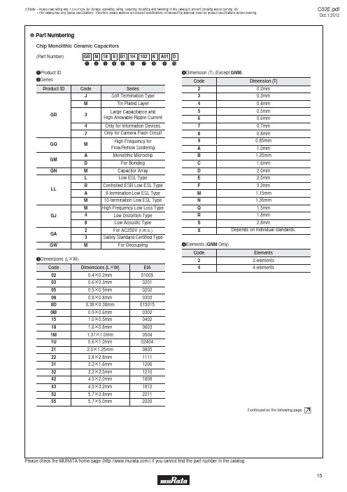
o Part Numbering
Chip Monolithic Ceramic Capacitors
(Part Number) qProduct ID wSeries Product ID GR ER GQ GM GN Code M 4 7 B M A M L LL C A M GJ M 6 GA GC 2 3 P M Series Tin Plated Layer Only for Information Devices / Tip & Ring Only for Camera Flash Circuit High Frequency Type High Frequency for Flow/Reflow Soldering Monolithic Microchip Capacitor Array Low ESL Wide Width Type Automotive Low ESL Wide Width Type Eight-termination Low ESL Type Ten-termination Low ESL Type High Frequency Low Loss Type Tin Plated Type High Frequency Low Loss Type for AC250V (r.m.s.) Safety Standard Recognized Type Automotive Soldering Electrode Automotive Tin Plated Layer GR q M w 18 e 8 B1 1H y 102 u K i A01 K o !0 rDimension (T) Code 2 2 3 4 5 6 7 8 9 A B C D E F M N R S Q X eDimension (LgW) Code 02 03 05 08 11 15 18 1D 1X 21 22 31 32 3X 42 43 52 55 Dimension (LgW) 0.4g0.2mm 0.6g0.3mm 0.5g0.5mm 0.8g0.8mm 1.25g1.0mm 1.0g0.5mm 1.6g0.8mm 1.4g1.4mm Depends on individual standards. 2.0g1.25mm 2.8g2.8mm 3.2g1.6mm 3.2g2.5mm 4.5g2.0mm 4.5g3.2mm 5.7g2.8mm 5.7g5.0mm 0805 1111 1206 1210 1808 1812 2211 2220
村田Murata LQ系列电感命名方式
B C D G H J K S W iFeatures Code Features Standard Type High-Q/ Low DC Resistance
Series LQG/LQP/LQW/LQH*1 LQW15A/18A/2BH
rApplications and Characteristics Code H M T A H H tCategory Code N S Category Standard Type Series LQG LQP LQW LQH Applications and Characteristics Multilayer Air-core Inductor (Coil) Film Type Film Type (Low DC Resistance Type) High Q Type (UHF-SHF) High Q Type (VHF-UHF) for High-frequency Resonant Circuit
RF Inductor Part Numbering
(Part Number)
LQ q
G w
15 e
H
N
1N0 y
S
0
2
D
yInductance Expressed by three-digit alphanumerics. The unit is micro-henry (µH). The first and second figures are significant digits, and the third figure expresses the number of zeros which follow the two figures. If there is a decimal point, it is expressed by the capital letter "R". In this case, all figures are significant digits. If inductance is less than 0.1µH, the inductance code is expressed by a combination of two figures and the capital letter "N", and the unit of inductance is nano-henry (nH). The capital letter "N" indicates the unit of "nH", and also expresses a decimal point. In this case, all figures are significant digits. uInductance Tolerance Code Inductance Tolerance ±0.1nH ±0.2nH ±0.5nH ±2% ±3% ±5% ±10% ±0.3nH ±0.05nH
各大品牌电容的命名规则

各大品牌电容的命名规则图1 SAMSUNG电容的命名图2 MURATA电容的命名图3 TDK电容的命名图4 KYOCERA电容的命名图5 TAIYO-YUDEN电容的命名图6 KEMET电容的命名图7 PANSONIC电容的命名图8 YAGEO/国巨电容的命名图9 华新(Walsin)电容的命名图10 风华电容的命名图11 宇阳电容的命名SOD/SOT系列产品1产能:400kk/月品种:开关二极管、稳压二极管、肖特基二极管、ESD保护二极管、达林顿三极管、高压三极管、普通三极管、数字三极管、稳压电路等。
封装:SOD-123 、SOD-323、SOD-523、SOT-23 、SOT-323、SOT-363 、SOT-523、SOT-89 、SOT-143、DFN表面安装器件产能:200kk/月品种:贴片整流二极管、快恢复二极管、超高速开关二极管、肖特基二极管、瞬态电压抑制二极管、固态放电管、双向触发二极管、贴片整流桥等。
封装:SOD-123FL 、DO-213AA 、DO-213AB 、SMAJ、SMA 、SMB 、SMC 、DB-1、DB-S 、TBS、MBM、MBS、SMAFL、TO-277A塑封二极管PlasticDiode产能:600kk/月品种:全系列塑封整流二极管、快恢复开关二极管、超高速二极管各类电器专用二极管、肖特基系列二极管、固态放电管二极管瞬态电压抑制二极管、双向触发二极管、变阻器二极管高反压二极管封装:R-1、A-405、A-405F、DO-41、DO-15、DO-15L、DO-15B R-3、DO-27、DO-27S、R-6汽车整流器AutomotiveRectifier产能:1kk/月品种:各类汽车整流器封装:AR 、ARS 、ZQA 、ZQB 、ZQL1 、ZQL2 、ZQL3 、ZQL4、CELL整流桥BridgeRectifier产能:3kk/月品种:桥式整流器、整流模块封装:KBPC、KBPC-W、WOM、KBP、KBJ、GBU、GBP、KBU、KBL、BR、BR-W 、MP、MP-W、SKBPC玻封二极管GlassDiode产能:60kk/月品种:小信号开关二极管稳压管小信号肖特基二极管封装:Mini Melf 、DO-34、DO-35。
村田电容命名规则
村田电容命名规则村田电容型号命名规则muRata村田制作所是电子元器件制造商。
主要制作贴片电容,电感,滤波器等产品,村田制作所的客户分布在PC、手机、汽车电子等领域。
智成电子村田一级代理商详细讲解村田电容型号的命名规则方法。
例如:贴片电容GRM32ER61A107ME20L(1210 X5R 10V 100UF 20%),下面我们把它分解开。
一、GR表示型号:村田贴片电容包含GC,GJ,GM,GQ,GR,KR,LL等二、M表示系列:村田贴片电容包含H,M,A,D,3,J,L三、32表示电容尺寸:村田贴片电容的尺寸包括0201-0402-0603-1206-1210-1812-2220(32是指尺寸长和宽3.2MM*2.5MM,就是我们熟知的1210电容)。
四、E表示厚度2.5MM,村田贴片电容常用的厚度5=0.5mm 6=0.6mm 8=0.8mm 9=0.9mm B=1.25mm C=1.6mm E=2.5mm五、R6代表材质X5R,村田贴片电容的材质常用材质村田代码有5C,R6,R7,F5等,具体的对应值如下:5C=COG/NPO/CH R6=X5R R7=X7R F5=Y5V5C工作温度是-55度+125度,温度系数是0+-30ppm/度;R6工作温度是-55度+85度,温度系数是+-15%;R7工作温度是-55度+125度,温度系数是+-15%;F5工作温度是-30度+85度。
温度系数是+22,-82%六、1A代表电压10V,村田贴片电容常用电压有0J,1A,1C,1E,1H等,对应值如下:0J=6.3V 1A=10V 1C=16V 1E=25V 1H=50V七、107代表容量100UF八、M代表精度+-20%,常用档位有B、C、D、J、K、M、Z,具体对应值如下:B=+-0.1pFC=+-0.25pF D=+-0.5pF J=+-5% K=+-10% M=+-20% Z=+80,-20%九、E20是村田内部代码,不重要。
muRata电感命名规则(可编辑修改word版)
m u R a t a电感命名规则
还是先举个例子吧,让大家先有个直观的了解: LQG15HS1N2S02D:这是 0402 封装的 1.2nH 电感,精度误差±0.3nH。
LQG15HS 是0402
封装的一个电感系列;
1N2 表示 1.2nH;
S 表示精度误差±0.3nH;
0 表示特征是“标准型”,LQG15HS 系列的这个数值都是 0;
2 表示电极是锡;
D 表示包装是纸带 (?180mm 卷盘)
详细的说明如下:
6,电感值
由 3 位字母数字表示。
单位为微亨(μH)。
第 1 位和第 2 位数字为有效数字,第 3 位数字表示有效数字后的 0 的个数。
有小数点时以大写字母"R"表示。
此时,所有数字均为有效数字。
如果电感值小于0.1μH,则电感值以两个数字和大写字母"N"的组合来表示,电感
w 结构值单位使用纳亨(nH)。
大写字母"N"表示单位"nH",同时含有 1 个小数点。
在这种情况时所有数字均为有效数字。
*1:不包括 LQM21N 系列
*2:不包括 LQH32 系列
9,电极
*1 不包括 LQH43C/LQH66S
*2 仅限 LQM21D(22 - 47μH)/LQM21F(4.7 - 47μH)/LQM21N(2.7 - 4.7μH)。
*3 仅限LQM21D(1.0 - 10μH)/LQM21F(1.0 - 2.2μH)/LQM21N(0.1 - 2.2μH)。
*4 不包括 LQP15T。
美国电子公司(Murata)电感产品说明书

Dimensions: [mm]Scale - 2:1Scale - 2:17447480151744748015174474801517447480151T e m p e r a t u r eT T T 7447480151Further informationComponent Libraries:Altium_WE-TI (22d)Downloads_CADENCE_WE-TI (22a)CadStar_WE-TI (19b)Eagle_WE-TI (19c)Download_IGS_WE-TI_1014PSpice_WE-TI (23a)Download_STP_WE-TI-1014Spectre_WE-TI (23a)Free Sample Order:Order free samples of this article directly here!Tutorials:■Single Coil Inductors (PDF)REDEXPERT:Calculate losses for 7447480151 in REDEXPERTWürth Elektronik eiSos GmbH & Co. KGEMC & Inductive SolutionsMax-Eyth-Str. 174638 WaldenburgGermanyCHECKED REVISION DATE (YYYY-MM-DD)GENERAL TOLERANCE PROJECTIONMETHODTRi004.0002023-12-14DIN ISO 2768-1mDESCRIPTIONWE-TI Radial Leaded Wire WoundInductor ORDER CODE7447480151SIZE/TYPE BUSINESS UNIT STATUS PAGED RA FTCautions and Warnings:The following conditions apply to all goods within the product series of WE-TI of Würth Elektronik eiSos GmbH & Co. KG:General:•This electronic component was designed and manufactured for use in general electronic equipment.•Würth Elektronik must be asked for written approval (following the PPAP procedure) before incorporating the components into any equipment in fields such as military, aerospace, aviation, nuclear control, submarine, transportation (automotive control, train control, ship control), transportation signal, disaster prevention, medical, public information network, etc. where higher safety and reliability are especially required and/or if there is the possibility of direct damage or human injury.•Electronic components that will be used in safety-critical or high-reliability applications, should be pre-evaluated by the customer. •The component is designed and manufactured to be used within the datasheet specified values. If the usage and operation conditions specified in the datasheet are not met, the wire insulation may be damaged or dissolved.•Do not drop or impact the components, the component may be damaged.•Würth Elektronik products are qualified according to international standards, which are listed in each product reliability report. Würth Elektronik does not warrant any customer qualified product characteristics beyond Würth Elektroniks’ specifications, for its validity and sustainability over time.•The customer is responsible for the functionality of their own products. All technical specifications for standard products also apply to customer specific products.Product specific:Soldering:•The solder profile must comply with the technical product specifications. All other profiles will void the warranty.•All other soldering methods are at the customers’ own risk.Cleaning and Washing:•Washing agents used during the production to clean the customer application might damage or change the characteristics of the wire insulation, marking or plating. Washing agents may have a negative effect on the long-term functionality of the product. Potting:•If the product is potted in the costumer application, the potting material might shrink or expand during and after hardening. Shrinking could lead to an incomplete seal, allowing contaminants into the core. Expansion could damage the components. We recommend a manual inspection after potting to avoid these effects. Storage Conditions:• A storage of Würth Elektronik products for longer than 12 months is not recommended. Within other effects, the terminals may suffer degradation, resulting in bad solderability. Therefore, all products shall be used within the period of 12 months based on the day of shipment.•Do not expose the components to direct sunlight.•The storage conditions in the original packaging are defined according to DIN EN 61760-2.•The storage conditions stated in the original packaging apply to the storage time and not to the transportation time of the components. Packaging:•The packaging specifications apply only to purchase orders comprising whole packaging units. If the ordered quantity exceeds or is lower than the specified packaging unit, packaging in accordance with the packaging specifications cannot be ensured. Handling:•Violation of the technical product specifications such as exceeding the nominal rated current will void the warranty.•Applying currents with audio-frequency signals might result in audible noise due to the magnetostrictive material properties. •Due to heavy weight of the components, strong forces and high accelerations might have the effect to damage the electrical connection or to harm the circuit board and will void the warranty.•Please be aware that products provided in bulk packaging may get bent and might lead to derivations from the mechanical manufacturing tolerances mentioned in our datasheet, which is not considered to be a material defect.•The temperature rise of the component must be taken into consideration. The operating temperature is comprised of ambient temperature and temperature rise of the component.The operating temperature of the component shall not exceed the maximum temperature specified.These cautions and warnings comply with the state of the scientific and technical knowledge and are believed to be accurate and reliable.However, no responsibility is assumed for inaccuracies or incompleteness.Würth Elektronik eiSos GmbH & Co. KGEMC & Inductive SolutionsMax-Eyth-Str. 174638 WaldenburgGermanyCHECKED REVISION DATE (YYYY-MM-DD)GENERAL TOLERANCE PROJECTIONMETHODTRi004.0002023-12-14DIN ISO 2768-1mDESCRIPTIONWE-TI Radial Leaded Wire WoundInductor ORDER CODE7447480151SIZE/TYPE BUSINESS UNIT STATUS PAGE D RA FTImportant NotesThe following conditions apply to all goods within the product range of Würth Elektronik eiSos GmbH & Co. KG:1. General Customer ResponsibilitySome goods within the product range of Würth Elektronik eiSos GmbH & Co. KG contain statements regarding general suitability for certain application areas. These statements about suitability are based on our knowledge and experience of typical requirements concerning the areas, serve as general guidance and cannot be estimated as binding statements about the suitability for a customer application. The responsibility for the applicability and use in a particular customer design is always solely within the authority of the customer. Due to this fact it is up to the customer to evaluate, where appropriate to investigate and decide whether the device with the specific product characteristics described in the product specification is valid and suitable for the respective customer application or not.2. Customer Responsibility related to Specific, in particular Safety-Relevant ApplicationsIt has to be clearly pointed out that the possibility of a malfunction of electronic components or failure before the end of the usual lifetime cannot be completely eliminated in the current state of the art, even if the products are operated within the range of the specifications.In certain customer applications requiring a very high level of safety and especially in customer applications in which the malfunction or failure of an electronic component could endanger human life or health it must be ensured by most advanced technological aid of suitable design of the customer application that no injury or damage is caused to third parties in the event of malfunction or failure of an electronic component. Therefore, customer is cautioned to verify that data sheets are current before placing orders. The current data sheets can be downloaded at .3. Best Care and AttentionAny product-specific notes, cautions and warnings must be strictly observed. Any disregard will result in the loss of warranty.4. Customer Support for Product SpecificationsSome products within the product range may contain substances which are subject to restrictions in certain jurisdictions in order to serve specific technical requirements. Necessary information is available on request. In this case the field sales engineer or the internal sales person in charge should be contacted who will be happy to support in this matter.5. Product R&DDue to constant product improvement product specifications may change from time to time. As a standard reporting procedure of the Product Change Notification (PCN) according to the JEDEC-Standard inform about minor and major changes. In case of further queries regarding the PCN, the field sales engineer or the internal sales person in charge should be contacted. The basic responsibility of the customer as per Section 1 and 2 remains unaffected.6. Product Life CycleDue to technical progress and economical evaluation we also reserve the right to discontinue production and delivery of products. As a standard reporting procedure of the Product Termination Notification (PTN) according to the JEDEC-Standard we will inform at an early stage about inevitable product discontinuance. According to this we cannot guarantee that all products within our product range will always be available. Therefore it needs to be verified with the field sales engineer or the internal sales person in charge about the current product availability expectancy before or when the product for application design-in disposal is considered. The approach named above does not apply in the case of individual agreements deviating from the foregoing for customer-specific products.7. Property RightsAll the rights for contractual products produced by Würth Elektronik eiSos GmbH & Co. KG on the basis of ideas, development contracts as well as models or templates that are subject to copyright, patent or commercial protection supplied to the customer will remain with Würth Elektronik eiSos GmbH & Co. KG. Würth Elektronik eiSos GmbH & Co. KG does not warrant or represent that any license, either expressed or implied, is granted under any patent right, copyright, mask work right, or other intellectual property right relating to any combination, application, or process in which Würth Elektronik eiSos GmbH & Co. KG components or services are used.8. General Terms and ConditionsUnless otherwise agreed in individual contracts, all orders are subject to the current version of the “General Terms and Conditions of Würth Elektronik eiSos Group”, last version available at .Würth Elektronik eiSos GmbH & Co. KGEMC & Inductive SolutionsMax-Eyth-Str. 174638 WaldenburgGermanyCHECKED REVISION DATE (YYYY-MM-DD)GENERAL TOLERANCE PROJECTIONMETHODTRi004.0002023-12-14DIN ISO 2768-1mDESCRIPTIONWE-TI Radial Leaded Wire WoundInductor ORDER CODE7447480151SIZE/TYPE BUSINESS UNIT STATUS PAGE D RA FT。
murata电容命名规则
murata电容命名规则【提纲】一、Murata电容简介Murata电容,源自日本,是全球领先的陶瓷电容器制造商。
凭借其精湛的工艺技术和严格的品质控制,Murata电容在电子元器件领域享有盛誉。
其产品广泛应用于消费电子、通讯、汽车电子、工业控制等领域。
【提纲】二、Murata电容命名规则详解1.命名格式Murata电容的命名格式为:品牌名(Murata)+ 容量(单位:pF)+ 工作电压(单位:V)+ 封装尺寸(如有)+ 型号(如有)。
2.参数含义- 容量:表示电容器存储电荷的能力,单位为皮法(pF)。
- 工作电压:表示电容器能承受的电压范围,单位为伏特(V)。
- 封装尺寸:表示电容器的物理尺寸,如0805、1206等。
- 型号:表示电容器的系列和特殊性能,如LR系列、HS系列等。
3.常用型号举例例如:Murata LR101C106M500J、Murata HS1612B104K500T等。
【提纲】三、如何选择合适的Murata电容1.容量选择:根据电路设计需求,选择适当容值的电容器。
一般来说,容量越大,电容器的储能能力越强,但体积也越大。
2.工作电压选择:根据电路的工作电压,选择合适的工作电压范围的电容器。
工作电压过高可能导致电容器损坏,过低则可能影响其储能效果。
3.封装尺寸选择:根据电路板的空间大小和安装方式,选择合适的封装尺寸。
常见的封装尺寸有0805、1206、1812等。
4.品质因数选择:品质因数(Q)是衡量电容器性能的重要指标,较高品质因数的电容器具有更好的稳定性、较低的损耗和更小的噪声。
根据电路对性能的要求,选择合适品质因数的电容器。
【提纲】四、应用领域及注意事项1.应用领域:Murata电容广泛应用于各类电子产品,如手机、平板、笔记本等,以及通讯、汽车电子、工业控制等领域。
2.注意事项:- 在高温、潮湿环境下,注意选择耐高温、防潮性能好的电容器。
- 电容器在使用过程中,注意电压、电流等参数的匹配,避免过载使用。
Murata Capacitor Naming Conventions Murata 陶瓷电容命名规范
!Note • Please read rating and !CAUTION (for storage, operating, rating, soldering, mounting and handling) in this catalog to prevent smoking and/or burning, etc.
C02E.pdf
Oct.1,2012
Continued from the preceding page.
tTemperature Characteristics Temperature Characteristic Codes Code 0C 1C 1X 2C 2P 2R 2S 2T 3C 3P 3R 3S 3T 3U 4C 4P 4R 4S 4T 4U 5C 5G 6C 6P 6R 6S 6T 7U B1 B3 C3 C6 C7 C8 D3 D6 D7 D8 E1 E4 E7 F1 F4 F5 J1 L8 Public STD Code CHA CG SL CH PH RH SH TH CJ PJ RJ SJ TJ UJ CK PK RK SK TK UK C0G X8G C0H P2H R2H S2H T2H U2J B *1 B C X5S X7S X6S D X5T X7T X6T Z5U X7U F *1 Z5V Y5V JA X8L *2 JIS JIS JIS JIS JIS JIS JIS JIS JIS JIS JIS JIS JIS JIS JIS JIS JIS JIS JIS EIA *2 EIA EIA EIA EIA EIA EIA JIS JIS JIS EIA EIA EIA JIS EIA EIA EIA EIA EIA JIS EIA EIA *2 *2 Temperature Characteristics Reference Temperature Capacitance Change or Temperature Temperature Range Coefficient 20°C 20°C 20°C 20°C 20°C 20°C 20°C 20°C 20°C 20°C 20°C 20°C 20°C 20°C 20°C 20°C 20°C 20°C 20°C 20°C 25°C 25°C 25°C 25°C 25°C 25°C 25°C 25°C 20°C 20°C 20°C 25°C 25°C 25°C 20°C 25°C 25°C 25°C 20°C 25°C 25°C 20°C 25°C 25°C 20°C 25°C 20 to 150°C 20 to 125°C 20 to 85°C 20 to 125°C 20 to 85°C 20 to 85°C 20 to 85°C 20 to 85°C 20 to 125°C 20 to 85°C 20 to 85°C 20 to 85°C 20 to 85°C 20 to 85°C 20 to 125°C 20 to 85°C 20 to 85°C 20 to 85°C 20 to 85°C 20 to 85°C 25 to 125°C 25 to 150°C 25 to 125°C 25 to 85°C 25 to 85°C 25 to 85°C 25 to 85°C 25 to 125°C *5 –25 to 85°C –25 to 85°C –25 to 85°C 85 to 125°C –55 to 85°C –55 to 125°C –55 to 105°C –25 to 125°C –55 to 125°C –55 to 125°C –55 to 105°C –25 to 85°C 10 to 85°C –55 to 125°C –25 to 85°C 10 to 85°C –30 to 85°C –25 to 105°C –55 to 150°C 0±60ppm/°C 0±30ppm/°C +350 to –1000ppm/°C 0±60ppm/°C –150±60ppm/°C –220±60ppm/°C –330±60ppm/°C –470±60ppm/°C 0±120ppm/°C –150±120ppm/°C –220±120ppm/°C –330±120ppm/°C –470±120ppm/°C –750±120ppm/°C 0±250ppm/°C –150±250ppm/°C –220±250ppm/°C –330±250ppm/°C –470±250ppm/°C –750±250ppm/°C 0±30ppm/°C 0±30ppm/°C 0±60ppm/°C –150±60ppm/°C –220±60ppm/°C –330±60ppm/°C –470±60ppm/°C –750±120ppm/°C ±10% ±10% ±20% +15%, –30% ±22% ±22% ±22% +20%, –30% +22%, –33% +22%, –33% +22%, –33% +20%, –55% +22%, –56% +22%, –56% +30%, –80% +22%, –82% +22%, –82% –20% max. +15%, –40% Operating Temperature Range –55 to 150°C –55 to 125°C –55 to 125°C –55 to 125°C –25 to 85°C –25 to 85°C –25 to 85°C –25 to 85°C –55 to 125°C –25 to 85°C –25 to 85°C –25 to 85°C –25 to 85°C –25 to 85°C –55 to 125°C –25 to 85°C –25 to 85°C –25 to 85°C –25 to 85°C –25 to 85°C –55 to 125°C –55 to 150°C –55 to 125°C –55 to 125°C –55 to 125°C –55 to 125°C –55 to 125°C –55 to 125°C –25 to 85°C –25 to 85°C –25 to 125°C –55 to 85°C –55 to 125°C –55 to 105°C –25 to 85°C –55 to 125°C –55 to 125°C –55 to 105°C –25 to 85°C 10 to 85°C –55 to 125°C –25 to 85°C –20 to 85°C –30 to 85°C –25 to 105°C –55 to 150°C Capacitance Change Each Temperature (%) –55°C Max. 0.82 0.54 0.82 1.37 2.56 0.58 0.58 0.87 2.33 3.02 4.09 5.46 8.78 Min. –0.45 –0.23 –0.45 –0.9 –1.88 –0.24 –0.24 –0.48 0.72 1.28 2.16 3.28 5.04 –25°C Max. 0.49 0.33 0.49 1.32 1.7 2.3 3.07 0.82 1.65 2.03 2.63 3.4 4.94 1.54 2.36 2.74 3.35 4.12 5.65 0.4 0.4 0.59 1.61 2.08 2.81 3.75 6.04 Min. –0.27 –0.14 –0.27 0.41 0.72 1.22 1.85 –0.54 0.14 0.45 0.95 1.58 2.84 –1.13 –0.45 –0.14 0.36 0.99 2.25 –0.17 –0.17 –0.33 0.5 0.88 1.49 2.26 3.47 –10°C Max. 0.33 0.22 0.33 0.88 1.13 1.54 2.05 0.55 1.1 1.35 1.76 2.27 3.29 1.02 1.57 1.83 2.23 2.74 3.77 0.25 0.25 0.38 1.02 1.32 1.79 2.39 3.84 Min. –0.18 –0.09 –0.18 0.27 0.48 0.81 1.23 –0.36 0.09 0.3 0.63 1.05 1.89 –0.75 –0.3 –0.09 0.24 0.66 1.5 –0.11 –0.11 –0.21 0.32 0.56 0.95 1.44 2.21 -
村田murata电感表示方式 中文版
2 4 56 13 26 39 4445 495658 63 68 72 79 81 941 2 3 4 5 6 7 8 9 10 11智芯恒科技温馨提示:请从正规渠道购买正品原装货!!23村田公司的LQ□系列片状线圈由小型、高性能电感构成。
其富有创新的线圈和外壳结构获得了低直流电阻和优良的高频特性。
该系列应用广泛,便于选择满足各种不同电路的元件。
4智芯恒科技温馨提示:请从正规渠道购买正品原装货!!开始LQH43M(N)2220LQH55DLQH31HLQH66S1212LQY33P智芯恒科技温馨提示:请从正规渠道购买正品原装货!!516(in mm)片状线圈 高频用多层型LQG15HN系列 (0402尺寸)LQG15HN系列是专门为高频应用设计的片状电感。
LQG15H系列采用集成层叠工艺制作,用于在高频范围实现稳定特性。
集成层叠工艺可实现很宽的电感值范围和低公差。
■特点1. 在高频段的高Q值和稳定电感的获得得益于独创的结构, 该结构将杂散电容降到最小。
适合移动通信设备中的高频 电路使用。
2. LQG15H尺寸小 (1.0×0.5×0.5mm),适合小而薄的移动 设备使用。
3. 外部电极为镍隔板结构,因此具有卓越的焊接耐热性。
4. 电感值范围宽1到10nH (E24标准) 10到120nH (E12标准)■用途1. 移动电话中的高频电路,如PA、ANT、VCO、SAW等2. 移动电话,如GSM、CDMA、PDC等3. “Bluetooth”4. 宽带网5. 一般高频电路■外形尺寸■额定值 (□: 包装代号)接下页。
动作温度范围: -55°C 到+125°C 仅可回流焊接。
智芯恒科技温馨提示:请从正规渠道购买正品原装货!!17Frequency (MHz)100806040200Q100100010000Frequency (MHz)1000100101I n d u ct a n c e (n H )接上页。
MURATA LQW18AN_00系列芯片电容器(芯片电感)产品说明书
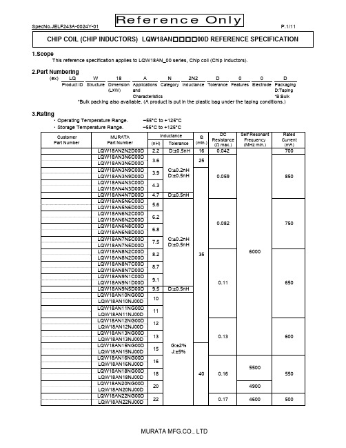
SpecNo.JELF243A-0024Y-01 P.1/11Reference OnlyCHIP COIL (CHIP INDUCTORS) LQW18AN □□□□00D REFERENCE SPECIFICATION1.ScopeThis reference specification applies to LQW18AN_00 series, Chip coil (Chip Inductors).2.Part Numbering(ex) LQ W 18 A N 2N2 D 0 0 DProduct ID Structure Dimension Applications Category Inductance Tolerance Features Electrode Packaging(L×W) andD:Taping Characteristics*B:Bulk *Bulk packing also available. (A product is put in the plastic bag under the taping conditions.)3.Rating・Operating Temperature Range. –55°C to +125°C ・Storage Temperature Range. –55°C to +125°CCustomer Part NumberMURATA Part NumberInductance Q (min.)DC Resistance (Ω max.)Self Resonant Frequency (MHz min.)Rated Current (mA)(nH)ToleranceLQW18AN2N2D00D 2.2D:±0.5nH 160.042 6000700LQW18AN3N6C00D 3.6C:±0.2nH D:±0.5nH250.059 850LQW18AN3N6D00D LQW18AN3N9C00D 3.935LQW18AN3N9D00D LQW18AN4N3C00D 4.3 LQW18AN4N3D00D LQW18AN4N7D00D 4.7D:±0.5nHLQW18AN5N6C00D 5.6C:±0.2nH D:±0.5nH0.082 750LQW18AN5N6D00D LQW18AN6N2C00D 6.2 LQW18AN6N2D00D LQW18AN6N8C00D 6.8 LQW18AN6N8D00D LQW18AN7N5C00D 7.5 LQW18AN7N5D00D LQW18AN8N2C00D 8.20.11 650LQW18AN8N2D00D LQW18AN8N7C00D 8.7 LQW18AN8N7D00D LQW18AN9N1C00D 9.1 LQW18AN9N1D00D LQW18AN9N5D00D 9.5D:±0.5nHLQW18AN10NG00D 10G:±2% J:±5%LQW18AN10NJ00D LQW18AN11NG00D 11 LQW18AN11NJ00D LQW18AN12NG00D 120.13 600LQW18AN12NJ00D LQW18AN13NG00D 13 LQW18AN13NJ00D LQW18AN15NG00D 1540 LQW18AN15NJ00D LQW18AN16NG00D 160.165500550LQW18AN16NJ00D LQW18AN18NG00D 18 LQW18AN18NJ00D LQW18AN20NG00D 204900LQW18AN20NJ00D LQW18AN22NG00D 220.17 4600 500LQW18AN22NJ00DSpecNo.JELF243A-0024Y-01 P.2/11Reference OnlyCustomerPart NumberMURATA Part NumberInductance Q (min.)DC Resistance (Ω max.)Self Resonant Frequency (MHz min.)Rated Current (mA)(nH)ToleranceLQW18AN24NG00D 24 G:±2%J:±5%400.213800 500LQW18AN24NJ00D LQW18AN27NG00D 27 3700 440 LQW18AN27NJ00D LQW18AN30NG00D 300.23 3300420LQW18AN30NJ00D LQW18AN33NG00D 33 3200 LQW18AN33NJ00D LQW18AN36NG00D 360.26 2900400LQW18AN36NJ00D LQW18AN39NG00D 39 2800 LQW18AN39NJ00D LQW18AN43NG00D 430.292700380LQW18AN43NJ00D LQW18AN47NG00D 47382600 LQW18AN47NJ00D LQW18AN51NG00D 51 0.33 2500 370LQW18AN51NJ00D LQW18AN56NG00D 56 0.35 2400 360LQW18AN56NJ00D LQW18AN62NG00D 62 0.51 2300 280LQW18AN62NJ00D LQW18AN68NG00D 68 0.38 2200 340 LQW18AN68NJ00D LQW18AN72NG00D 72340.56 2100270LQW18AN72NJ00D LQW18AN75NG00D 75 2050LQW18AN75NJ00D LQW18AN82NG00D 82 0.60 2000 250LQW18AN82NJ00D LQW18AN91NG00D 91 0.64 1900 230 LQW18AN91NJ00D LQW18ANR10G00D 1000.68 1800 220 LQW18ANR10J00D LQW18ANR11G00D 110321.2 1700 200 LQW18ANR11J00D LQW18ANR12G00D 120 1.3 1600 180 LQW18ANR12J00D LQW18ANR13G00D 130 1.4 1450 170 LQW18ANR13J00D LQW18ANR15G00D 150 1.5 1400 160 LQW18ANR15J00D LQW18ANR16G00D 1602.1 1350 150 LQW18ANR16J00D LQW18ANR18G00D 18025 2.2 1300 140 LQW18ANR18J00D LQW18ANR20G00D 200 2.4 1250120LQW18ANR20J00D LQW18ANR22G00D 220 2.5 1200LQW18ANR22J00D LQW18ANR27G00D 270303.4 960 110 LQW18ANR27J00D LQW18ANR33G00D 3305.580085LQW18ANR33J00D LQW18ANR39G00D 390 6.2 80 LQW18ANR39J00D LQW18ANR47G00D 4707.0 700 75LQW18ANR47J00DSpecNo.JELF243A-0024Y-01 P.3/11Reference Only4. Testing Conditions《Unless otherwise specified》《In case of doubt》Temperature : Ordinary Temperature / 15°C to 35°C Temperature: 20°C±2°CHumidity : Ordinary Humidity / 25%(RH) to 85%(RH) Humidity : 60%(RH) to 70%(RH)Atmospheric Pressure : 86kPa to 106 kPa5.Appearance and Dimensions■Unit Mass (Typical value)0.003g(in mm).Reference OnlySpecNo.JELF243A-0024Y-01 P.4/11SpecNo.JELF243A-0024Y-01 P.5/11Reference Only8.Environmental Performance It shall be soldered on the substrate.No. Item Specification Test Method 8.1 Heat Resistance Appearance:No damage Inductance Change: within ±5% Q Change: within ±20% Temperature:125°C±2°CTime:1000h (+48h,0h) Then measured after exposure in the room condition for 24h±2h.8.2 Cold Resistance Appearance:No damage Inductance Change: within ±5% Q Change: within ±20%Temperature:-55°C±2°CTime:1000h (+48h,-0h) Then measured after exposure in the roomcondition for 24h±2h.8.3 Humidity Temperature:40°C±2°CHumidity:90%(RH) to 95%(RH) Time:1000h (+48h,-0h)Then measured after exposure in the room condition for 24h±2h.8.4 Temperature Cycle 1 cycle:1 step:-55°C±2°C / 30min±3 min2 step:Ordinary temp. / 10min to 15 min3 step:+125°C±2°C / 30min±3 min4 step:Ordinary temp. / 10min to15 min Total of 10 cyclesThen measured after exposure in the room condition for 24h±2h.9.Specification of Packaging9.1 Appearance and Dimensions of paper tape (8mm-wide)(in mm)9.2 Specification of Taping(1) Packing quantity (standard quantity)4,000 pcs. / reel(2) Packing MethodProducts shall be packed in the cavity of the base tape and sealed by top tape and bottom tape. (3) Sprocket holeThe sprocket holes are to the right as the tape is pulled toward the user. (4) Spliced pointBase tape and Top tape has no spliced point. (5) Missing components numberMissing components number within 0.1 % of the number per reel or 1 pc., whichever is greater, and are not continuous. The Specified quantity per reel is kept.9.3 Pull StrengthTop tape 5N min.Bottom tape4.0±0.1φ1.5±2.0±0.054.0±0.1Direction of feed1.1max.1.0±0.051.8±0.058.0±0.23.5±0.051.75±0.10.10SpecNo.JELF243A-0024Y-01 P.6/11Reference Only9.4 Peeling off force of cover tapeSpeed of Peeling off 300mm/min Peeling off force0.1N to 0.6N(minimum value is typical)9.5 Dimensions of Leader-tape,Trailer and ReelThere shall be leader-tape ( top tape and empty tape) and trailer-tape (empty tape) as follows.9.6 Marking for reelCustomer part number, MURATA part number, Inspection number(∗1) ,RoHS Marking (∗2), Quantity etc ・・・∗1) <Expression of Inspection No.> □□ OOOO ×××(1) (2) (3)(1) Factory code(2) Date First digit: Year / Last digit of yearSecond digit: Month / Jan. to Sep. → 1 to 9, Oct. to Dec. → O, N, D Third, Fourth digit : Day(3) Serial No.∗2) <Expression of RoHS Marking >ROHS – Y (△)(1) (2)(1) RoHS regulation conformity parts.(2) MURATA classification number9.7 Marking for Outside package (corrugated paper box)Customer name, Purchasing order number, Customer part number, MURATA part number, RoHS Marking (∗2) ,Quantity, etc ・・・9.8. Specification of Outer CaseOuter Case Dimensions(mm)Standard Reel Quantityin Outer Case (Reel)W D H 186 186 93 5∗ Above Outer Case size is typical. It depends on a quantity of an order.10. ! CautionLimitation of ApplicationsPlease contact us before using our products for the applications listed below which require especially high reliability for the prevention of defects which might directly cause damage to the third party's life, body or property.(1) Aircraft equipment (6) Transportation equipment (vehicles, trains, ships, etc.) (2) Aerospace equipment (7) Traffic signal equipment (3) Undersea equipment (8) Disaster prevention / crime prevention equipment (4) Power plant control equipment (9) Data-processing equipment (5) Medical equipment (10) Applications of similar complexity and /or reliability requirements to the applications listed in the aboveF165to 180degreeTop tapeBottom tape Base tapeWDLabelHSpecNo.JELF243A-0024Y-01 P.7/11Reference Only11. NoticeProducts can only be soldered with reflow.This product is designed for solder mounting.Please consult us in advance for applying other mounting method such as conductive adhesive.11.1 Land pattern designingRecommended land patterns for reflow soldering are as follows:These have been designed for Electric characteristics and solderability.Please follow the recommended patterns. Otherwise, their performance which includes electrical performance or solderability may be affected, or result to "position shift" in soldering process.(in mm)11.2 Flux, Solder・Use rosin-based flux.Includes middle activator equivalent to 0.06(wt)% to 0.1(wt)% Chlorine.Don’t use highly acidic flux with halide content exceeding 0.2(wt)% (chlorine conversion value). Don’t use water-soluble flux. ・Use Sn-3.0Ag-0.5Cu solder.・Standard thickness of solder paste : 100μm to 150μm.11.3 Reflow soldering conditions・Pre-heating should be in such a way that the temperature difference between solder and product surface is limited to 150°C max. Cooling into solvent after soldering also should be in such a way that the temperature difference is limited to 100°C max.Insufficient pre-heating may cause cracks on the product, resulting in the deterioration of products quality.・Standard soldering profile and the limit soldering profile is as follows.The excessive limit soldering conditions may cause leaching of the electrode and / or resulting in the deterioration of product quality.・Reflow soldering profileStandard Profile Limit Profile Pre-heating 150°C ~180°C 、90s ±30s Heating above 220°C 、30s ~60s above 230°C 、60s max. Peak temperature 245°C ±3°C 260°C,10s Cycle of reflow 2 times 2 timesA 0.6 to 0.8B 1.9 to 2.0 C0.7 to 1.0Limit ProfileStandard Profile90s±30s230℃260℃245℃±3℃220℃30s ~60s60s max.180150Temp.(s)(℃)Time.resistSpecNo.JELF243A-0024Y-01 P.8/11Reference Only11.4 Reworking with soldering ironThe following conditions must be strictly followed when using a soldering iron.Pre-heating 150°C,1 min Tip temperature 350°C max. Soldering iron output 80W max. Tip diameter φ3mm max. Soldering time 3(+1,-0)sTime 2 timesNote :Do not directly touch the products with the tip of the soldering iron in order to prevent thecrack on the products due to the thermal shock.11.5 Solder Volume・Solder shall be used not to be exceeded the upper limits as shown below.・Accordingly increasing the solder volume, the mechanical stress to Chip is also increased. Exceeding solder volume may cause the failure of mechanical or electrical performance.1/3T ≦t ≦TT :thickness of product11.6 Product’s locationThe following shall be considered when designing and laying out P.C.B.'s.(1) P.C.B. shall be designed so that products are not subject to the mechanical stress due to warping the board.[Products direction ]Products shall be located in the sidewaysdirection (Length:a <b) to the mechanical stress.(2) Components location on P.C.B. separation.It is effective to implement the following measures, to reduce stress in separating the board.It is best to implement all of the following three measures; however, implement as many measures as possible to reduce stress.Contents of MeasuresStress Level (1) Turn the mounting direction of the component parallel to the board separation surface. A > D *1 (2) Add slits in the board separation part.A >B (3) Keep the mounting position of the component away from the board separation surface. A > C*1 A > D is valid when stress is added vertically to the perforation as with Hand Separation.If a Cutting Disc is used, stress will be diagonal to the PCB, therefore A > D is invalid.〈Poor example〉〈Good example〉baSeamSlitADBCbaLength:a <bReference OnlySpecNo.JELF243A-0024Y-01 P.9/11(3) Mounting Components Near Screw HolesWhen a component is mounted near a screw hole, it may be affected by the board deflection that occurs duringthe tightening of the screw. Mount the component in a position as far away from the screw holes as possible.11.7 Cleaning ConditionsProducts shall be cleaned on the following conditions.(1) Cleaning temperature shall be limited to 60°C max.(40°C max for IPA)(2) Ultrasonic cleaning shall comply with the following conditions with avoiding the resonancephenomenon at the mounted products and P.C.B.Power : 20 W / l max. Frequency : 28kHz to 40kHz Time : 5 min max.(3) Cleaner1. Alcohol type cleanerIsopropyl alcohol (IPA)2. Aqueous agentPINE ALPHA ST-100S(4) There shall be no residual flux and residual cleaner after cleaning.In the case of using aqueous agent, products shall be dried completely after rinse with de-ionizedwater in order to remove the cleaner.(5) Other cleaning Please contact us.11.8 Resin coatingThe inductance value may change due to high cure-stress of resin to be used for coating/molding products.An open circuit issue may occur by mechanical stress caused by the resin, amount/cured shape of resin, oroperating condition etc. Some resin contains some impurities or chloride possible to generate chlorine byhydrolysis under some operating condition may cause corrosion of wire of coil, leading to open circuit.So, please pay your careful attention in when you select resin in case of coating/molding the productswith the resin.Prior to use the coating resin, please make sure no reliability issue is observed by evaluating productsmounted on your board.11.9 Caution for use・Sharp material such as a pair of tweezers or other material such as bristles of cleaning brush , shall not be touched to the winding portion to prevent the breaking of wire.・Mechanical shock should not be applied to the products mounted on the board to prevent the breaking of the core.11.10 Notice of product handling at mountingIn some mounting machines,when picking up components support pin pushes up the components from thebottom of base tape. In this case, please remove the support pin. The support pin may damage the componentsand break wire.In rare case ,the laser recognition can not recognize this component. Please contact us when you use laserrecognition. (There is no problem with the permeation and reflection type.)11.11 Handling of a substrateAfter mounting products on a substrate, do not apply any stress to the product caused by bending or twisting to thesubstrate when cropping the substrate, inserting and removing a connector from the substrate or tightening screwto the substrate.Excessive mechanical stress may cause cracking in the product.Bending TwistingReference OnlySpecNo.JELF243A-0024Y-01 P.10/1111.12 Storage and Handing Requirements(1) Storage periodUse the products within 12 months after delivered.Solderability should be checked if this period is exceeded.(2) Storage conditions・Products should be stored in the warehouse on the following conditions.Temperature :-10°C to 40°CHumidity :15% to 85% relative humidity No rapid change on temperature and humidity・Don't keep products in corrosive gases such as sulfur,chlorine gas or acid, or it may causeoxidization of electrode, resulting in poor solderability.・Products should not be stored on bulk packaging condition to prevent the chipping of thecore and the breaking of winding wire caused by the collision between the products.・Products should be stored on the palette for the prevention of the influence from humidity,dust and so on.・Products should be stored in the warehouse without heat shock, vibration, direct sunlight and so on.(3) Handling ConditionCare should be taken when transporting or handling product to avoid excessive vibration ormechanical shock.12.! Note(1)Please make sure that your product has been evaluated in view of your specifications with our product beingmounted to your product.(2)You are requested not to use our product deviating from the reference specifications.(3)The contents of this reference specification are subject to change without advance notice.Please approve our product specifications or transact the approval sheet for product specificationsbefore ordering.Reference OnlySpecNo.JELF243A-0024Y-01 P.11/11Mouser ElectronicsAuthorized DistributorClick to View Pricing, Inventory, Delivery & Lifecycle Information:M urata:LQW18AN10NG00D LQW18AN10NJ00D LQW18AN11NG00D LQW18AN11NJ00D LQW18AN12NG00D LQW18AN12NJ00D LQW18AN13NG00D LQW18AN13NJ00D LQW18AN15NG00D LQW18AN15NJ00D LQW18AN16NG00D LQW18AN16NJ00D LQW18AN18NG00D LQW18AN18NJ00D LQW18AN20NG00D LQW18AN20NJ00D LQW18AN22NG00D LQW18AN22NJ00D LQW18AN24NG00D LQW18AN24NJ00D LQW18AN27NG00D LQW18AN27NJ00D LQW18AN2N2D00D LQW18AN30NG00D LQW18AN30NJ00D LQW18AN33NG00D LQW18AN33NJ00D LQW18AN36NG00D LQW18AN36NJ00D LQW18AN39NG00D LQW18AN3N6C00D LQW18AN3N6D00D LQW18AN3N9C00D LQW18AN3N9D00D LQW18AN43NG00D LQW18AN43NJ00D LQW18AN47NG00D LQW18AN47NJ00D LQW18AN4N3C00D LQW18AN4N3D00D LQW18AN4N7D00D LQW18AN51NG00D LQW18AN51NJ00D LQW18AN56NG00D LQW18AN56NJ00D LQW18AN5N6C00D LQW18AN5N6D00D LQW18AN62NG00D LQW18AN62NJ00D LQW18AN68NG00D LQW18AN68NJ00D LQW18AN6N2C00D LQW18AN6N2D00D LQW18AN6N8C00D LQW18AN6N8D00D LQW18AN72NG00D LQW18AN72NJ00D LQW18AN75NG00D LQW18AN75NJ00D LQW18AN7N5D00D LQW18AN82NG00D LQW18AN82NJ00D LQW18AN8N2D00D LQW18AN8N7D00D LQW18AN91NG00D LQW18AN91NJ00D LQW18AN9N1D00D LQW18AN9N5D00D LQW18ANR10G00D LQW18ANR10J00D LQW18ANR11G00D LQW18ANR11J00D LQW18ANR12G00D LQW18ANR12J00D LQW18ANR13G00D LQW18ANR13J00D LQW18ANR15G00D LQW18ANR15J00D LQW18ANR16G00D LQW18ANR16J00D LQW18ANR18G00D LQW18ANR18J00D LQW18ANR20G00D LQW18ANR20J00D LQW18ANR22G00D LQW18ANR22J00D LQW18ANR27G00D LQW18ANR27J00D LQW18ANR33G00D LQW18ANR33J00D LQW18ANR39G00D LQW18ANR39J00D LQW18ANR47G00D LQW18ANR47J00D LQW18AN9N1C00D LQW18AN8N7C00D LQW18AN7N5C00D LQW18AN8N2C00D。
MURATA LQM18FN_00系列芯片导线(芯片电感)商品说明书
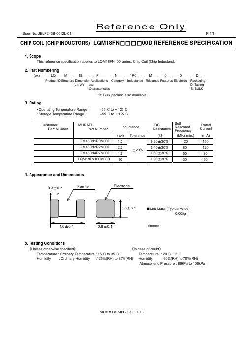
CHIP COIL (CHIP INDUCTORS)LQM18FN□□□□00D REFERENCE SPECIFICATION1. ScopeThis reference specification applies to LQM18FN_00 series, Chip Coil (Chip Inductors).2. Part Numbering(ex) LQ M 18 F N 1R0 M 0 0 DProduct ID Structure Dimension Applications Category Inductance T olerance Features Electrode Packaging(L×W) and D: TapingCharacteristics *B: BULK*B: Bulk packing also available3. Rating・Operating Temperature Range –55°C to + 125°C・Storage Temperature Range –55°C to + 125°CCustomerPart Number MURATAPart Number InductanceDCResistanceSelfResonantFrequencyRatedCurrent(μH) Tolerance (Ω) (MHzmin.)(mA)LQM18FN1R0M00D1.0±20% 0.20±30% 120 150LQM18FN2R2M00D2.2 0.40±30% 80 120LQM18FN4R7M00D4.7 0.60±30% 50 80LQM18FN100M00D10 0.90±30% 30 50 4.Appearance and Dimensions■Unit Mass (Typical value)(in mm)5. Testing Conditions《Unless otherwise specified》《In case of doubt》Temperature : Ordinary Temperature / 15°C to 35°C Temperature: 20°C ± 2°CHumidity : Ordinary Humidity / 25%(RH) to 85%(RH) Humidity : 60%(RH) to 70%(RH)Atmospheric Pressure : 86kPa to 106kPa6. Electrical Performance7. Mechanical PerformanceNo. Item Specification Test Method7.4 Solderability The wetting area of the electrodeshall be at least 90% covered with new solder coating.Flux: Ethanol solution of rosin 25(wt)% (Immersed for 5s to 10s) Solder: Sn-3.0Ag-0.5CuPre-Heating: 150°C±10°C / 60s to 90s Solder Temperature: 240°C±5°C Immersion Time: 3s±1s7.5 Resistance toSoldering Heat Appearance: No damageInductance Change: within ±20%Flux: Ethanol solution of rosin 25(wt)% (Immersed for 5s to 10s) Solder: Sn-3.0Ag-0.5CuPre-Heating: 150°C±10°C / 60s to 90s Solder Temperature: 270°C±5°C Immersion Time: 10s±1sThen measured after exposure in the room condition for 24h±2h.8. Environmental PerformanceIt shall be soldered on the substrate. No. Item Specification Test Method8.1 Heat Resistance Appearance: No damageInductance Change: within ±20% Temperature: 125°C±2°C Time: 1000h (+48h, -0h)Then measured after exposure in the room condition for 48h±2h. 8.2 HumidityTemperature: 40°C±2°CHumidity: 90%(RH) to 95%(RH) Time: 1000h (+48h, -0h)Then measured after exposure in the room condition for 48h±2h. 8.3 TemperatureCycleAppearance: No damageInductance Change: within ±30%1 cycle:1 step: -55°C±2°C / 30 min±3 min2 step: Ordinary temp. / 10 min to 15 min3 step: +125°C±2°C / 30 min±3 min4 step: Ordinary temp. / 10 min to15 min Total of 10 cyclesThen measured after exposure in the room condition for 48h±2h.9. Specification of Packaging9.1 Appearance and Dimensions of paper tape (8mm-wide)(in mm)φ1.5±Direction of feed1.1m ax1.85±0.18.0±0.33.5±0.050.14.0±0.12.0±0.054.0±0.11.75±0.11.05±0.19.2 Specification of Taping(1) Packing quantity (standard quantity)4,000 pcs. / reel(2) Packing MethodProducts shall be packed in the cavity of the base tape and sealed by top tape and bottom tape. (3) Sprocket holeThe sprocket holes are to the right as the tape is pulled toward the user. (4) Spliced pointBase tape and Top tape has no spliced point. (5) Missing components numberMissing components number within 0.1% of the number per reel or 1 pc., whichever is greater, and are not continuous. The Specified quantity per reel is kept.9.3 Pull StrengthTop tape5N min.Bottom tape9.4 Peeling off force of top tape Speed of Peeling off 300mm/ minPeeling off force 0.1 to 0.6N(minimum value is typical)9.5 Dimensions of Leader-tape, Trailer and ReelThere shall be leader-tape ( top tape and empty tape) and trailer-tape (empty tape) as follows.9.6 Marking for reelCustomer part number, MURATA part number, Inspection number (*1), RoHS Marking (*2), Quantity etc ・・・*1) <Expression of Inspection No.> □□ OOOO ⨯⨯⨯(1) (2) (3)(1) Factory Code (2) Date First digit : Year / Last digit of yearSecond digit : Month / Jan. to Sep. → 1 to 9, Oct. to Dec. → O, N, D Third, Fourth digit : Day(3) Serial No.*2) <Expression of RoHS Marking> ROHS – Y (△)(1) (2)(1) RoHS regulation conformity parts. (2) MURATA classification numberF 165to 180degree Top tape Bottom tape Base tape9.7 Marking for Outside package (corrugated paper box)Customer name, Purchasing order number, Customer part number, MURATA part number, RoHS Marking (*2), Quantity, etc ・・・9.8. Specification of Outer CaseOuter Case Dimensions(mm)Standard Reel Quantityin Outer Case (Reel)W D H 186 186 93 5* Above Outer Case size is typical. It depends on a quantity of an order.10. ! CautionLimitation of ApplicationsPlease contact us before using our products for the applications listed below which require especially high reliability for the prevention of defects which might directly cause damage to the third party's life, body or property.(1) Aircraft equipment (6) Transportation equipment (vehicles, trains, ships, etc.) (2) Aerospace equipment (7) Traffic signal equipment(3) Undersea equipment (8) Disaster prevention / crime prevention equipment (4) Power plant control equipment (9) Data-processing equipment (5) Medical equipment (10) Applications of similar complexity and /or reliability requirements to the applications listed in the above11. NoticeThis product is designed for solder mounting.Please consult us in advance for applying other mounting method such as conductive adhesive.11.1 Land pattern designingSoldering a b cFlow 0.8 2.50.7Ref low 0.7 2.0(in mm)11.2 Flux, Solder・Use rosin-based flux.Don’t use highly acidic flux with halide content exceeding 0.2(wt) % (chlorine conversion value). Don’t use water-soluble flux. ・Use Sn-3.0Ag-0.5Cu solder.・Standard thickness of solder paste: 100μm to 150μm.11.3 Flow soldering / Reflow soldering conditions・Pre-heating should be in such a way that the temperature difference between solder and product surface is limited to 150°C max. Cooling into solvent after soldering also should be in such a way that the temperature difference is limited to 100°C max.Insufficient pre-heating may cause cracks on the product, resulting in the deterioration of products quality.・Standard soldering profile and the limit soldering profile is as follows.The excessive limit soldering conditions may cause leaching of the electrode and/or resulting in the deterioration of product quality.ResistWDLabelHSoldering profile(1) Flow soldering profile(2) Reflow soldering profile11.4 Reworking with soldering ironThe following conditions must be strictly followed when using a soldering iron.Pre-heating 150°C,1 min Tip temperature 350°C max. Soldering iron output 80W max. Tip diameter φ3mm max. Soldering time 3(+1, -0)sTime 2 timesNote : Do not directly touch the products with the tip of the soldering iron in order to prevent the crack onthe products due to the thermal shock.11.5 Solder Volume・Solder shall be used not to be exceeded the upper limits as shown below.・Accordingly increasing the solder volume, the mechanical stress to Chip is also increased. Exceeding solder volume may cause the failure of mechanical or electrical performance.1/3T ≦t ≦T T : thickness of product11.6 Product’s locationThe following shall be considered when designing and laying out P .C.B.'s.(1) P .C.B. shall be designed so that products are not subject to the mechanical stress due to warping the board.[Products direction ]Products shall be located in the sideways direction (Length: a‹b) to the mechanical stress.(2)Components location on P .C.B. separation. It is effective to implement the following measures, to reduce stress in separating the board.It is best to implement all of the following three measures; however, implement as many measures as possible to reduce stress. Contents of Measures Stress Level (1) Turn the mounting direction of the component parallel to the board separation surface. A > D *1 (2) Add slits in the board separation part. A > B (3) Keep the mounting position of the component away from the board separation surface. A > C*1 A > D is valid when stress is added vertically to the perforation as with Hand Separation. If a Cutting Disc is used, stress will be diagonal to the PCB, therefore A > D is invalid.(3) Mounting Components Near Screw HolesWhen a component is mounted near a screw hole, it may be affected by the board deflection that occurs during the tightening of the screw. Mount the component in a position as far away from the screw holes as possible.11.7 Cleaning ConditionsProducts shall be cleaned on the following conditions.(1) Cleaning temperature shall be limited to 60°C max. (40°C max for IPA)(2) Ultrasonic cleaning shall comply with the following conditions with avoiding the resonance phenomenon at the mounted products and P .C.B.Power : 20 W / l max. Frequency : 28kHz to 40kHz Time : 5 min max.(3) Cleaner1. Alcohol type cleaner Isopropyl alcohol (IPA)2. Aqueous agent PINE ALPHA ST-100S〈Poor example 〉〈Good example 〉ba(4) There shall be no residual flux and residual cleaner after cleaning.In the case of using aqueous agent, products shall be dried completely after rinse with de-ionized water in order to remove the cleaner.(5) Other cleaning Please contact us.11.8 Resin coatingInductance value may be changed due to the large cure-stress of the resin when products are coated with resin. In this case, take care when you select resin to prevent the deterioration of the product quality.11.9 Caution for useThere is possibility that the inductance value change due to magnetism. Don‘t use a magnet or a pair of tweezers with magnetism when chip coil are handled. (The tip of the tweezers should be molded with resin or pottery.)11.10 Magnetic SaturationWhen the excessive current over rated current is applied, the inductance value may change due to magnetism.11.11 Handling of a substrateAfter mounting products on a substrate, do not apply any stress to the product caused by bending ortwisting to the substrate when cropping the substrate, inserting and removing a connector from thesubstrate or tightening screw to the substrate.Excessive mechanical stress may cause cracking in the product.Bending Twisting11.12 Storage and Handing Requirements(1) Storage periodUse the products within 6 months after delivered.Solderability should be checked if this period is exceeded.(2) Storage conditions・Products should be stored in the warehouse on the following conditions.Temperature :-10°C to 40°CHumidity :15% to 85% relative humidity No rapid change on temperature and humidityDon't keep products in corrosive gases such as sulfur,chlorine gas or acid, or it may cause oxidization ofelectrode, resulting in poor solderability.・Products should be stored on the palette for the prevention of the influence from humidity, dust and soon.・Products should be stored in the warehouse without heat shock, vibration, direct sunlight and so on.・Products should be stored under the airtight packaged condition.(3) Handling ConditionCare should be taken when transporting or handling product to avoid excessive vibration or mechanicalshock.12.! Note(1) Please make sure that your product has been evaluated in view of your specifications with our productbeing mounted to your product.(2) You are requested not to use our product deviating from the reference specifications.(3) The contents of this reference specification are subject to change without advance notice.Please approve our product specifications or transact the approval sheet for product specificationsbefore ordering.。
陶瓷贴片电容、贴片电感、片式磁珠命名规则与基本知识
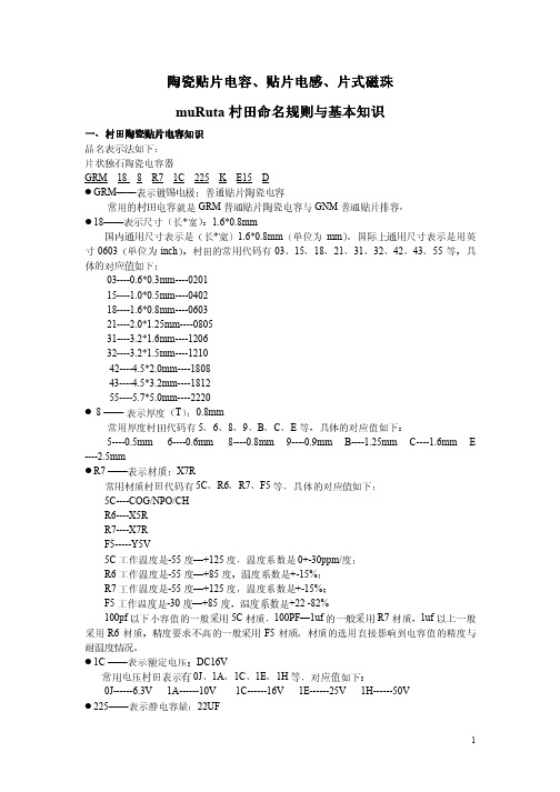
陶瓷贴片电容陶瓷贴片电容、、贴片电感贴片电感、、片式磁珠 muRuta 村田命名规则与基本知识一、村田陶瓷贴片电容知识品名表示法如下: 片状独石陶瓷电容器GRM 18 8 R7 1C 225 K E15 D GRM——表示镀锡电极:普通贴片陶瓷电容常用的村田电容就是GRM 普通贴片陶瓷电容与GNM 普通贴片排容。
18——表示尺寸(长*宽):1.6*0.8mm国内通用尺寸表示是(长*宽)1.6*0.8mm (单位为mm )。
国际上通用尺寸表示是用英寸0603(单位为inch ),村田的常用代码有03、15、18、21、31、32、42、43、55等,具体的对应值如下:03----0.6*0.3mm----0201 15----1.0*0.5mm----0402 18----1.6*0.8mm----0603 21----2.0*1.25mm----0805 31----3.2*1.6mm----1206 32----3.2*1.5mm----1210 42----4.5*2.0mm----1808 43----4.5*3.2mm----1812 55----5.7*5.0mm----22208 —— 表示厚度(T ):0.8mm 常用厚度村田代码有5、6、8、9、B 、C 、E 等,具体的对应值如下:5----0.5mm 6----0.6mm 8----0.8mm 9----0.9mm B----1.25mm C----1.6mm E ----2.5mmR7 ——表示材质:X7R常用材质村田代码有5C 、R6、R7、F5等,具体的对应值如下: 5C----COG/NPO/CH R6----X5R R7----X7R F5-----Y5V5C 工作温度是-55度—+125度,温度系数是0+-30ppm/度; R6工作温度是-55度—+85度,温度系数是+-15%; R7工作温度是-55度—+125度,温度系数是+-15%; F5工作温度是-30度—+85度,温度系数是+22 -82%100pf 以下小容值的一般采用5C 材质,100PF—1uf 的一般采用R7材质,1uf 以上一般采用R6材质,精度要求不高的一般采用F5材质。
- 1、下载文档前请自行甄别文档内容的完整性,平台不提供额外的编辑、内容补充、找答案等附加服务。
- 2、"仅部分预览"的文档,不可在线预览部分如存在完整性等问题,可反馈申请退款(可完整预览的文档不适用该条件!)。
- 3、如文档侵犯您的权益,请联系客服反馈,我们会尽快为您处理(人工客服工作时间:9:00-18:30)。
muRata电感命名规则
还是先举个例子吧,让大家先有个直观的了解:
LQG15HS1N2S02D:这是0402封装的1.2nH电感,精度误差±0.3nH。
LQG15HS是0402封装的一个电感系列;
1N2表示1.2nH;
S表示精度误差±0.3nH;
0表示特征是“标准型”,LQG15HS系列的这个数值都是0;
2表示电极是锡;
D表示包装是纸带 (?180mm卷盘)
详细的说明如下:
6,电感值
由3位字母数字表示。
单位为微亨(μH)。
第1位和第2位数字为有效数字,第3位数字表示有效数字后的0的个数。
有小数点时以大写字母"R"表示。
此时,所有数字均为有效数字。
如果电感值小于0.1μH,则电感值以两个数字和大写字母"N"的组合来表示,电感
w结构值单位使用纳亨(nH)。
大写字母"N"表示单位"nH",同时含有1个小数点。
在这种情况时所有数字均为有效数字。
*1:不包括LQM21N系列*2:不包括LQH32系列9,电极
*1不包括LQH43C/LQH66S
*2仅限LQM21D(22 - 47μH)/LQM21F(4.7 - 47μH)/LQM21N(2.7 - 4.7μH)。
*3仅限LQM21D(1.0 - 10μH)/LQM21F(1.0 - 2.2μH)/LQM21N(0.1 - 2.2μH)。
*4不包括LQP15T。