JESD22-B117A Solder Ball Shear(锡球剪切力测试标准)
JESD22-B102E (Solderability)

6
Table 4 Altitude versus Steam Temperature
7
Figures
Figure 1 Inspection Area for Dual Inline Packages
13
Figure 2 Inspection Area for Gull Wing Packages
14
viewpoint. Within the JEDEC organization there are procedures whereby a JEDEC standard or publication may be further processed and ultimately become an ANSI standard.
Organizations may obtain permission to reproduce a limited number of copies through entering into a license agreement. For information, contact:
JEDEC Solid State Technology Association 2500 Wilson Boulevard
9
5.3 Method 2. Surface Mount Process Simulation Test
12
6 Summary
16
Annex A
17
Tables
Table 1 Precondition Conditions for Solderability Testing
1
Table 2 Maximum Limits of Solder Bath Contaminant
JESD22-B117A 锡球剪切
JEDECSTANDARDSolder Ball Shear锡球剪切JESD22-B117A(Revision of JESD22-B117, July 2000)OCTOBER 2006JEDEC SOLID STATE TECHNOLOGY ASSOCIATION测试方法B117:锡球剪切(从JEDEC委员会选票及JCB-06-37制定下,对包装设备的可靠性试验方法由JC-14.1小组委员会认定。
)1 范围这种测试方法适用于焊球结束前使用的附着物剪切力测试。
焊球分别剪切;力量和失效模式下的数据收集和分析。
在本文件包括低速和高速测试。
这个试验的目的是进行评估锡球能够承受机械剪切的能力,可能在器件制造、处理、检验、运输和最终使用的作用力。
焊料球剪切是一种破坏性试验。
2 术语和定义剪切力:适用于一个方向平行于设备平面到焊料球的力量。
测试仪器:测试仪器用于应用剪切力焊锡球。
剪切工具:一个刚硬的工具,直接对着在焊球剪切(见图1)。
剪切工具集成了传感元件,使剪切力可以测量。
剪切工具支架:设备平面和剪切工具刀之间的距离(见图1)。
夹具:剪切测试时夹具固定焊球在设备上(见图5)。
剪切速度:剪切刀具移动速率去剪焊锡球。
低速剪切:剪切速度通常是0.0001 - 0.0008米/秒(100 - 800微米/秒)。
高速剪切:剪切速度是一般为0.01 - 1.0米/秒,但可以超出这个范围。
回流后经过时间:焊球剪切和焊料球最后回流之间经过的时间。
失效模式:类型或锡球剪切后观察到的失效位置。
后压力测试:锡球剪切后进行可靠性评估,如温度循环或高温储存压力测试。
3 仪器剪切力测量设备应使用经过校准的传感器或传感元件。
应进行定期校准,以确保精度长期一致。
建议设备的最大负载能力至少为测量球在被测试部分的剪切最大值的10%。
该仪器可专门用于焊球剪切试验,或用于通用负载偏移量测试仪器。
该设备必须能够有施加到锡球的应用和记录。
该设备必须有能力用于一个已知位移速率的负载能力。
JESD22~B117A中文版
JEDECSTANDARDSolder Ball Shear锡球剪切JESD22-B117A (Revision of JESD22-B117, July 2000)OCTOBER 2006JEDEC SOLID STATE TECHNOLOGY ASSOCIATION测试方法B117:锡球剪切(从JEDEC委员会选票及JCB-06-37制定下,对包装设备的可靠性试验方法由JC-14.1小组委员会认定。
)1 围这种测试方法适用于焊球结束前使用的附着物剪切力测试。
焊球分别剪切;力量和失效模式下的数据收集和分析。
在本文件包括低速和高速测试。
这个试验的目的是进行评估锡球能够承受机械剪切的能力,可能在器件制造、处理、检验、运输和最终使用的作用力。
焊料球剪切是一种破坏性试验。
2 术语和定义剪切力:适用于一个方向平行于设备平面到焊料球的力量。
测试仪器:测试仪器用于应用剪切力焊锡球。
剪切工具:一个刚硬的工具,直接对着在焊球剪切(见图1)。
剪切工具集成了传感元件,使剪切力可以测量。
剪切工具支架:设备平面和剪切工具刀之间的距离(见图1)。
夹具:剪切测试时夹具固定焊球在设备上(见图5)。
剪切速度:剪切刀具移动速率去剪焊锡球。
低速剪切:剪切速度通常是0.0001 - 0.0008米/秒(100 - 800微米/秒)。
高速剪切:剪切速度是一般为0.01 - 1.0米/秒,但可以超出这个围。
回流后经过时间:焊球剪切和焊料球最后回流之间经过的时间。
失效模式:类型或锡球剪切后观察到的失效位置。
后压力测试:锡球剪切后进行可靠性评估,如温度循环或高温储存压力测试。
3 仪器剪切力测量设备应使用经过校准的传感器或传感元件。
应进行定期校准,以确保精度长期一致。
建议设备的最大负载能力至少为测量球在被测试部分的剪切最大值的10%。
该仪器可专门用于焊球剪切试验,或用于通用负载偏移量测试仪器。
该设备必须能够有施加到锡球的应用和记录。
该设备必须有能力用于一个已知位移速率的负载能力。
JESD22-B101中文版
测试方法B101 外观检查1. 目的本测试的目的是验证材料、设计、施工、标记和设备的工艺应符合采购文档要求的适用性。
外部目测是一种无损检测方法,适用于所有包装类型。
该测试适用于鉴定、过程、监控或批量验收两者都有。
2.仪器在本测试中使用的设备应能够证明设备符合要求。
3.过程设备应按照适用的要求进行检验采购文件及第4条所列的准则。
当外国材料有问题时,设备可能受到干净的过滤气流(吸力或每秒88英尺,最大,并重新检查。
4. 失败的标准设备有下列情形之一的,视为故障:(a)设备设计、引线标识、标记(内容、位置和易读性)、材料、构造和工艺与采购文档不一致;(b)明显的腐蚀、污染或破损迹象[严重弯曲或破损]、引线、破裂密封(玻璃半月板除外)、有缺陷(剥落、剥落或起泡)或损坏的电镀或裸露的金属基底。
(由剥落、点蚀或腐蚀引起的成品变色);(c)不完整或与未与正常位置对齐的引脚;非正常的引脚弯曲;以及(对于带状引脚)扭曲超过了正常引脚平面之外;(d)有任何不符合详图或适用采购文件的情况,或有任何会影响设备的正常使用的未知特性、损坏、腐蚀或污染的情况。
(e)因制造、搬运、测试或下列原因造成的缺陷或损坏:(1)包装破损。
表面划伤不应成为失效原因,除非它们违反了本协议规定的标记、表面处理等其他标准。
(2)任何在表面任何方向上超过0.060英寸(1.52毫米)以及表面损伤深度超过受影响元件厚度25% (上盖、底托或侧面) 的情况。
(3)任何暴露密封玻璃(在此之前未暴露)或任何设计不打算暴露的引线框材料的缺口。
5.总结下列细节应在适用的采购文件中说明:(a)标记和引线或引脚识别的要求(见4.)。
(b)材料、设计、施工和工艺的详细要求(见4.)。
(c)样本量和质量等级。
JESD22简介+目录列表

JESD22标准定义及意义详细如下JESD22-A101orJESD22-A110.3. A101稳态温湿度偏置寿命JESD22-A101-BPublished:Apr-1997STEADY-STATETEMPERATUREHUMIDITYBIASLIFETEST: Thisstandardestablishesadefinedmethodandconditionsf orperformingatemperaturehumiditylifetestwithbiasapplied.Thetestisusedtoevaluatethereliabilityofnonhermeticpackagedsolidstatedevicesinhumidenvironments.Itemployshightem peratureandhumidityconditionstoacceleratethepenetrati onofmoisturethroughexternalprotectivematerialoralongi nterfacesbetweentheexternalprotectivecoatingandcondu ctorsorotherfeatureswhichpassthroughit.Thisrevisionen hancestheabilitytoperformthistestonadevicewhichcanno tbebiasedtoachieveverylowpowerdissipation.JESD22-A101-B发布:1997 年8 月稳态温湿度偏置寿命试验本标准建立了一个定义的方法,用于进行一个施加偏置电压的温湿度寿命试验。
本试验用于评估非气密封装固态器件在潮湿环境下的可靠性。
试验采用高温和高湿条件以加速水汽对外部保护材料或沿着外部保护材料和外部保护涂层,贯通其的导体或其他部件的穿透作用。
JESD22-B117A中文版
JEDECSTANDARDSolder Ball Shear锡球剪切JESD22-B117A(Revision of JESD22-B117, July 2000)OCTOBER 2006JEDEC SOLID STATE TECHNOLOGY ASSOCIATION测试方法B117:锡球剪切(从JEDEC委员会选票及JCB-06-37制定下,对包装设备的可靠性试验方法由JC-14.1小组委员会认定。
)1 范围这种测试方法适用于焊球结束前使用的附着物剪切力测试。
焊球分别剪切;力量和失效模式下的数据收集和分析。
在本文件包括低速和高速测试。
这个试验的目的是进行评估锡球能够承受机械剪切的能力,可能在器件制造、处理、检验、运输和最终使用的作用力。
焊料球剪切是一种破坏性试验。
2 术语和定义剪切力:适用于一个方向平行于设备平面到焊料球的力量。
测试仪器:测试仪器用于应用剪切力焊锡球。
剪切工具:一个刚硬的工具,直接对着在焊球剪切(见图1)。
剪切工具集成了传感元件,使剪切力可以测量。
剪切工具支架:设备平面和剪切工具刀之间的距离(见图1)。
夹具:剪切测试时夹具固定焊球在设备上(见图5)。
剪切速度:剪切刀具移动速率去剪焊锡球。
低速剪切:剪切速度通常是0.0001 - 0.0008米/秒(100 - 800微米/秒)。
高速剪切:剪切速度是一般为0.01 - 1.0米/秒,但可以超出这个范围。
回流后经过时间:焊球剪切和焊料球最后回流之间经过的时间。
失效模式:类型或锡球剪切后观察到的失效位置。
后压力测试:锡球剪切后进行可靠性评估,如温度循环或高温储存压力测试。
3 仪器剪切力测量设备应使用经过校准的传感器或传感元件。
应进行定期校准,以确保精度长期一致。
建议设备的最大负载能力至少为测量球在被测试部分的剪切最大值的10%。
该仪器可专门用于焊球剪切试验,或用于通用负载偏移量测试仪器。
该设备必须能够有施加到锡球的应用和记录。
该设备必须有能力用于一个已知位移速率的负载能力。
22B110B板级机械冲击

JEDECSTANDARDMechanical Shock – Component and SubassemblyJESD22-B110B(Revision of JESD22-B110A, November 2004, Reaffirmed: June 2009)JULY 2013JEDEC SOLID STATE TECHNOLOGY ASSOCIATIONNOTICEJEDEC standards and publications contain material that has been prepared, reviewed, and approved through the JEDEC Board of Directors level and subsequently reviewed and approvedby the JEDEC legal counsel.JEDEC standards and publications are designed to serve the public interest through eliminating misunderstandings between manufacturers and purchasers, facilitating interchangeability and improvement of products, and assisting the purchaser in selecting and obtaining with minimum delay the proper product for use by those other than JEDEC members, whether the standard is tobe used either domestically or internationally.JEDEC standards and publications are adopted without regard to whether or not their adoption may involve patents or articles, materials, or processes. By such action JEDEC does not assume any liability to any patent owner, nor does it assume any obligation whatever to parties adoptingthe JEDEC standards or publications.The information included in JEDEC standards and publications represents a sound approach to product specification and application, principally from the solid state device manufacturer viewpoint. Within the JEDEC organization there are procedures whereby a JEDEC standard or publication may be further processed and ultimately become an ANSI standard.No claims to be in conformance with this standard may be made unless all requirements stated inthe standard are met.Inquiries, comments, and suggestions relative to the content of this JEDEC standard or publication should be addressed to JEDEC at the address below, or refer to under Standards and Documents for alternative contact information.Published by©JEDEC Solid State Technology Association 20133103 North 10th StreetSuite 240 SouthArlington, VA 22201-2107This document may be downloaded free of charge; however JEDEC retains thecopyright on this material. By downloading this file the individual agrees not tocharge for or resell the resulting material.PRICE: Contact JEDECPrinted in the U.S.A.All rights reservedPLEASE!DON’T VIOLATETHELAW!This document is copyrighted by JEDEC and may not bereproduced without permission.For information, contact:JEDEC Solid State Technology Association3103 North 10th StreetSuite 240 SouthArlington, VA 22201-2107or refer to under Standards-Documents/Copyright Information.JEDEC Standard No. 22-B110BPage 1TEST METHOD B110BMECHANICAL SHOCK– COMPONENT AND SUBASSEMBLY(From JEDEC Board Ballot JCB-13-27, formulated under the cognizance of the JC-14.1 Subcommittee on Reliability Test Methods for Packaged Devices.)1 ScopeComponent and Subassembly Mechanical Shock Test Method is intended to evaluate components in the free state and assembled to printed wiring boards for use in electrical equipment. The method is intended to determine the compatibility of components and subassemblies to withstand moderately severe shocks. The use of subassemblies is a means to test components in usage conditions as assembled to printed wiring boards. Mechanical Shock due to suddenly applied forces, or abrupt change in motion produced by handling, transportation or field operation may disturb operating characteristics, particularly if the shock pulses are repetitive. This is a destructive test intended for component qualification.2 ApparatusThe shock-testing apparatus shall be capable of providing shock pulses with a peak acceleration of up to 2900 multiples of gravity (g), a velocity change of 100 to 544 centimeters per second (39 to 214 inches per second), and a pulse duration between 0.3 and 8.0 milliseconds to the body of the component. For free-state testing, a velocity change of 125 to 544 centimeters per second (49 to 214 inches per second) and a pulse duration between 0.3 and 2.0 milliseconds is sufficient. Conversely, for mounted-state testing, apparatus capable of a velocity change of 100 to 544 centimeters per second (39 to 214 inches per second) and a pulse duration between 5.0 and 8.0 milliseconds to the body of the component is sufficient.The acceleration pulse shall be a half-sine waveform with an allowable deviation from specified peak acceleration not greater than ±10%. The test velocity change shall be ±10% of the specified level. The pulse duration shall be measured between the points at 10% of the peak acceleration during rise time and 10% of the peak acceleration during decay time. Absolute tolerances of the pulse duration shall be ±15% of the specified duration. The test equipment transducer shall have a natural frequency greater than 5 times the frequency of the shock pulse being established, and measured through a low-pass filter having a bandwidth greater than 5 times the frequency of the shock pulse being established. Filtering should not be used in lieu of good measurement setup and procedure practices.Appropriate equipment calibration should be considered prior to any testing to ensure conformance to the specified targets and acceptable tolerances. Reserving a set of known good units is recommended for pre-test calibration exercise whenever new samples are to be tested. If calibration tests are conducted regularly, then following periodical preventive maintenance should suffice for the equipment to meet the target and tolerance limits.Test Method B110B(Revision of Test Method B110A)JEDEC Standard No. 22-B110BPage 23 Terms and definitionsc omponent: A constituent part.NOTE 1 Examples include integrated circuits as attached components and surface-mounted-subassembly components of printed circuit boards.NOTE 2 The classification of an item as a device or a component depends upon the intention of the owner at the time of classification.dead-bug (orientation): The orientation of a package with the terminals facing up.deviation from specified acceleration [velocity change] [pulse duration] level: The maximum difference between the measured value and the target value.equivalent drop height: The free-fall drop height from which an object at rest must fall, in vacuum, under standard gravity, to attain a velocity equal to the velocity change stated in the test specification. NOTE This is the theoretical height that will impart the specified velocity change if impact with zero rebound occurs. This height is provided for reference only in the various service conditions.free state (of a component): The state in which a component or subassembly is rigidly attached to the test apparatus so that the full specified shock level is transmitted to the component or subassembly body. live-bug (orientation): The orientation of a package with the terminals facing down , e.g., resting on its terminals.mounted state: The state in which a subassembly is supported by a test fixture that allows flexure to simulate usage conditions and in a manner such that the full specified shock level is transmitted to the subassembly body.peak acceleration: The maximum acceleration during the dynamic motion of the sample under test.pulse duration: The time interval between the instant when the acceleration first reaches 10% of its specified peak level and the instant when the acceleration first returns to 10% of the specified peak level after having reached that peak level.NOTE The basic frequency of the pulse is 1/ (2 x duration).service condition: The designation for the severity of stress.subassembly: A printed circuit board and the components assembled thereon that form a unit or segment of electrical equipment.NOTE The components are preferably located near the center of the printed circuit board.velocity change: The integral of the acceleration interval over the duration of the entire shock event including at least the pulse duration interval.vertical direction: The direction that is parallel with gravity, i.e., normal to the normalized surface of the earth.Test Method B110B(Revision of Test Method B110A)4 PThe shock before us apparatus to a total duration s directions subassemb accelerati in each of 2 define thThere are a componCompone In the free full specif is perform componen a process such proc Procedure k-testing appa e. Means sha . In the free sof 30 shocksspecified in ts of three orth bly shall be on, velocity c f the positive he componen Figu Figure 2two types of nent or subass ents or s ubas e-state, the co fied shock lev med, the meth nt or subassem or processes esses in the te aratus shall b all be provide state unless o s, which are f the selected s hogonal axes subjected to change and p and negative nt orientation, re 1 — Live facing d 2 — Dead b facing u f tests that can embly in the ssemblies sub omponent or vel is transmi hod of moun mbly rework,should be apest hardware be attached to ed to prevent otherwise spe five shock pu service condi s (X, Y and Z o a total of pulse duration e directions of positive and bug orientat ownward in bug orientat pward in ei n be performe free-state, an bjected to the subassembly itted to the co nting to the t reuse, remou pplied to the cpreparation s o a sturdy lab t the shock f cified, the co ulses of the p ition (see Tab Z). If shock t 12 shocks, n specified in f three orthog negative dire tion with sold either free o tion with sol ither free or ed, based on t nd another is t test shall be r shall be rigid omponent or est apparatus unting, burn i component orhall be docum A1A1 boratory table from being re omponent or peak accelerat ble 1) in eac testing is req which are t the selected gonal axes (X ections for the der spheres o or mounted sRotalive-b lder sphere r mounted s the test inform testing of a su randomly sel dly attached t subassembly s shall be typ in, or other str r subassembly mented.JEDEC Stan (Revision of T e or equivalen epeated due t subassembly tion, velocity ch of the pos quired in the two shock p service cond X, Y and Z). F e three orthogof componen state.ate clockwise bug to dead-b es of compon state.mation needed ubassembly in ected and typ to the test app y body. If the pical of the u ressful proces y prior to the ndard No. 22-B P Test Method B Test Method B nt base and le to “bounce” i shall be subj y change and sitive and neg mounted stat ulses of the dition (see Tab Figure 1 and F gonal axes. nt– bugnentd. One is testi n a mounted-s pical of produ paratus, so th mounted stat usage conditi ss is possible e shock test. U B110BPage 3B110B110A)eveled in thejected pulse gative te, the peak ble 2) Figure ing ofstate. uction. hat the te test ion. If , such Use ofJEDEC Standard No. 22-B110BPage 4Test Method B110B(Revision of Test Method B110A)4.1 Component or subassembly in free-stateComponents or subassemblies to be tested in the free- state must be subjected to at least one of the service conditions (A to H) shown in Table 1, which shall be documented. The designated shock shall be applied to the component or subassembly body in a manner to simulate expected impacts during processing, packaging, and shipment. The component or subassembly shall be rigidly attached to the test apparatus in such a manner that it experiences the full-specified shock level at the component or subassembly body. At least five shocks in each of two directions of three orthogonal axes shall be applied (minimum total of 30 shocks) at the severity of the designated service condition.Table 1 — Component or subassembly free state test levelsNOTE velocity change = 2 * (std_g * acceleration_peak_g * pulse_duration) / pidrop height = 0.5 * (velocity_change)2 / std_g4.2 Subassembly in mounted stateIf required, subassemblies shall also be tested in a mounted state, subject to at least one of the service conditions (1 to 14) shown in Table 2, which shall be documented. The designated shock shall be applied to the subassembly mounted to the test apparatus with fixtures that allow flexure to simulate the usage conditions, and in a manner such that the full specified shock level is transmitted to the subassembly body. Preferred methods to support the subassembly are a slotted/clamping 'picture frame', or a raised-boss bolted fixture with contact points in four regions not closer than one inch from any component. The subassembly, supporting method, test fixture mounting dimensions, and one or more of the lowest resonant frequencies of the subassembly shall be documented. At least two shocks in each of two directions of three orthogonal axes shall be applied (minimum total of 12 shocks) at the severity of the designated service condition.The optimum test is performed when the subassembly is mounted in a manner that simulates the application configuration. If that information is unknown or unavailable, a recommended printed wiring board for testing the component(s) of the subassembly is the JEDEC standard thermal card (as described in JEDEC Standards JESD51-9, JESD51-10, and JESD51-11), which should be modified to include component and connection functionality circuitry.ServiceconditionAcceleration peak Pulse duration Velocity change Equivalent drop height g ms cm/s in/s cm inches H2900 0.3 543 214 150 59 G2000 0.4 499 197 127 50 B 1500 0.5 468 184 112 44F 900 0.7 393 155 78.9 31A 500 1.0 312 123 49.7 20E 340 1.2 255 100 33.1 13D 200 1.5 187 73.7 17.9 7C 100 2.0 125 49.2 7.90 3JEDEC Standard No. 22-B110BPage 5Test Method B110B(Revision of Test Method B110A)4.2 Subassembly in mounted state (cont’d)Alternately, if the size or construction of the JEDEC thermal card is not suitable for the given component(s), a printed wiring board should be used with the dimensions, materials, and construction typical for the component subassembly usage, and should include electrical circuitry to test for functionality, continuity, and damage of the component on the subassembly. The dimensions and construction of the printed wiring board shall be documented. Test results using subassembly application hardware are most relevant and should take precedence over results obtained using test vehicles. Table 2 — Subassembly mounted state test levelsServiceconditionAcceleration peak Pulse duration Velocity change Equivalent drop height g ms cm/s in/s cm inches 1109 8.0 544 214 151 60 2108 7.5 506 199 130 51 3 107 7.0 468 184 111 444 105 6.5 426 168 92.6 365 103 6.0 386 152 75.9 306 95 5.8 344 135 60.3 247 86 5.6 301 118 46.1 188 72 5.4 243 95.6 30.0 129 67 5.3 222 87.3 25.1 1010 61 5.2 198 78.0 20.0 811 54 5.1 172 67.7 15.1 612 45 5.0 140 55.3 10.1 413 39 5.0 122 47.9 7.6 314 32 5.0 100 39.3 5.1 2NOTE velocity change = 2 * (std_g * acceleration_peak_g * pulse_duration) / pidrop height = 0.5 * (velocity_change)2 / std_g4.3 MeasurementsHermeticity tests, if required, visual examination and electrical measurements (consisting of parametric and functional tests) shall be performed.JEDEC Standard No. 22-B110BPage 6Test Method B110B(Revision of Test Method B110A) 5 Failure criteriaA component or subassembly shall be considered as a failure if hermeticity requirements, if any, cannot be demonstrated, if parametric limits are exceeded or if functionality cannot be demonstrated under the conditions specified in the applicable procurement document. Mechanical damage, such as cracking, chipping or breaking of portions of the component shall also be considered a failure provided such damage was not caused by fixturing or handling and the damage is critical to performance in the specific application. Subassembly failure criteria may include, but is not limited to, solder connections to the printed wiring board, compliant pin leads, adhesive, encapsulation, or underfill that materially affect component or subassembly reliability.6 SummaryThe following details shall be specified in the applicable procurement document:a) Test service condition, for each test performed.b) Electrical measurements.c) Sample size and accept number.d) Disposition of failures.e) Hermetic leak rate (if applicable).f) Description of mounted state test vehicle and fixture (if applicable).g) Description of component pre-test stress history (if applicable).JEDEC Standard No. 22-B110BPage 7 Annex A (informative) Differences between JESD22-B110B and JESD22-B110AA.1 Differences between JESD22-B110B and JESD22-B110AThe following list briefly describes most of the changes made to entries that appear in this publication, JESD22-B110B, compared to its predecessor, JESD22-B110A (November 2004, reaffirmed June 2009). Clause Description of ChangeAll Combined Mechanical Shock JESD22-B104C into this standard to establish one document covering unattached components and components attached to printed wiring boards.2 Modified tolerance limits: peak acceleration reduced from ±20% to ±10%; pulse duration reduced from ±30% to ±15%.3 Updated Terms and definitions.4 Added Figures 1 and 2.4.1 Updated Table 1: mathematical formulas added for velocity change and equivalent drop height; calculated values shown in table.4.2 Updated Table 2: mathematical formulas added for velocity change and equivalent drop height; calculated values shown in table; portable subassembly conditions removed.JEDEC Standard No. 22-B110B Page 8StandarThe purporegarding JEDEC. AIf you canJEDEC Attn: Publ 3103 Nort Suite 240Arlington,1. I reco RT The r UO2. Reco3. OtherSubmitted Name: Company Address:City/Staterd Improve ose of this fo usage of the All comments n provide inpu lications Depa th 10thStreet SouthVA 22201-2ommend chan Requirement,Test method referenced cla UnclearOther mmendations r suggestions d by y:e/Zip: ement Form orm is to prov e subject sta s will be collec ut, please com artment2107nges to the fo , clause numbnumber ause number Too Rigid s for correctio s for documenm vide the Tech andard. Indiv cted and disp mplete this for llowing: berhas proven to In Eon: nt improveme hnical Commit viduals or com persed to the a rm and return Fax: 70Clause numb o be:Error nt:JEDE ttees of JEDE mpanies are appropriate c to:03.907.7583ber Phone:E-mail:Date:EC JESD2EC with inpu invited to su committee(s). 22-B110Bt from the ind ubmit comme dustry nts to。
电子封装锡和锡合金表面晶须标准研究
电子封装锡和锡合金表面晶须标准研究发布时间:2022-05-09T08:14:17.102Z 来源:《新型城镇化》2022年9期作者:杨雅丽曲乐[导读] 本文简述了晶须的来源,形成机理及抑制措施,并结合JEDEC的标准对锡晶须标准制定进行指导。
珠海格力电器股份有限公司广东珠海 519000摘要:在当前电子封装行业,锡和锡合金易于产生锡须致使电器发生故障是一直以来困扰的难题,随着环保要求的提高,在锡中添加铅可以抑制锡晶须的生长已经不再是解决这一难题的绝佳方案,因此对锡晶须标准的研究成为必不可少的课题。
本文简述了晶须的来源,形成机理及抑制措施,并结合JEDEC的标准对锡晶须标准制定进行指导。
1引言锡和锡合金由于本身物理特性,易于在表面形成晶须致使电器发生故障,这一现象严重阻碍了电子封装行业的发展,尤其在航空航天、军事等高精端应用场景中,这一难题始终悬而未决。
而在实际应用过程中,针对晶须建立相关标准对于评价其使用性能尤为重要,因此对晶须的标准研究也是电子封装中必不可少的课题。
本文结合JESD22-A121A和JESD201A标准,即锡和锡合金表面晶须生长测量的测试方法、锡和锡合金表面涂层的锡须灵敏度环境验收要求,深入对锡晶须标准分析研究。
2晶须来源晶须是指一种呈纤维状的晶体,均匀的横截面积是其主要特征。
锡晶须则是在锡或锡合金表面自发生长出的晶须。
电子器件使用过程中晶须的存在造成相邻导体间短路、晶须短路导致金属蒸发放电等。
晶须的形成机理一直是业界研究的重点也是难点问题,目前尚无公认一致的结论。
目前提出的生长机制主要有位错机制、再结晶机制、氧化膜破裂(COT)机制、金属间化合物氧化分解机制、氢致晶须生长机制5种。
基于对晶须生长机制的探讨研究,提出了合金化、去应力退火[1]、中间隔离层、镀后重熔[2]、有机涂层、电镀工艺改进等几种锡晶须的抑制措施。
尽管目前除添加铅元素外还发现一些抑制锡晶须的措施,但仍无可量产并实现产业性抑制晶须的措施,锡晶须的产生无可避免,因此亟需建立对电子元器件中锡晶须的标准要求。
JESD22-B101中文版
JESD22-B101中文版测试方法B101 外观检查1. 目的本测试的目的是验证材料、设计、施工、标记和设备的工艺应符合采购文档要求的适用性。
外部目测是一种无损检测方法,适用于所有包装类型。
该测试适用于鉴定、过程、监控或批量验收两者都有。
2.仪器在本测试中使用的设备应能够证明设备符合要求。
3.过程设备应按照适用的要求进行检验采购文件及第4条所列的准则。
当外国材料有问题时,设备可能受到干净的过滤气流(吸力或每秒88英尺,最大,并重新检查。
4. 失败的标准设备有下列情形之一的,视为故障:(a)设备设计、引线标识、标记(内容、位置和易读性)、材料、构造和工艺与采购文档不一致;(b)明显的腐蚀、污染或破损迹象[严重弯曲或破损]、引线、破裂密封(玻璃半月板除外)、有缺陷(剥落、剥落或起泡)或损坏的电镀或裸露的金属基底。
(由剥落、点蚀或腐蚀引起的成品变色);(c)不完整或与未与正常位置对齐的引脚;非正常的引脚弯曲;以及(对于带状引脚)扭曲超过了正常引脚平面之外;(d)有任何不符合详图或适用采购文件的情况,或有任何会影响设备的正常使用的未知特性、损坏、腐蚀或污染的情况。
(e)因制造、搬运、测试或下列原因造成的缺陷或损坏:(1)包装破损。
表面划伤不应成为失效原因,除非它们违反了本协议规定的标记、表面处理等其他标准。
(2)任何在表面任何方向上超过0.060英寸(1.52毫米)以及表面损伤深度超过受影响元件厚度25% (上盖、底托或侧面) 的情况。
(3)任何暴露密封玻璃(在此之前未暴露)或任何设计不打算暴露的引线框材料的缺口。
5.总结下列细节应在适用的采购文件中说明:(a)标记和引线或引脚识别的要求(见4.)。
(b)材料、设计、施工和工艺的详细要求(见4.)。
(c)样本量和质量等级。
JESD22-B117A Solder Ball Shear(锡球剪切力测试标准)
Inquiries, comments, and suggestions relative to the content of this JEDEC standard or publication should be addressed to JEDEC at the address below, or call (703) 907-7559 or
be used either domestically or internationally.
JEDEC standards and publications are adopted without regard to whether or not their adoption may involve patents or articles, materials, or processes. By such action JEDEC does not assume any liability to any patent owner, nor does it assume any obligation whatever to parties adopting
JEDEC STANDARD
Solder Ball Shear
JESБайду номын сангаас22-B117A
(Revision of JESD22-B117, July 2000) OCTOBER 2006
JEDEC SOLID STATE TECHNOLOGY ASSOCIATION
JESD22-B117A中文版

JEDECSTANDARDSolder Ball Shear锡球剪切JESD22-B117A(Revision of JESD22-B117, July 2000)OCTOBER 2006JEDEC SOLID STATE TECHNOLOGY ASSOCIATION测试方法B117:锡球剪切(从JEDEC委员会选票及JCB-06-37制定下,对包装设备的可靠性试验方法由JC-14.1小组委员会认定。
)1 范围这种测试方法适用于焊球结束前使用的附着物剪切力测试。
焊球分别剪切;力量和失效模式下的数据收集和分析。
在本文件包括低速和高速测试。
这个试验的目的是进行评估锡球能够承受机械剪切的能力,可能在器件制造、处理、检验、运输和最终使用的作用力。
焊料球剪切是一种破坏性试验。
2 术语和定义剪切力:适用于一个方向平行于设备平面到焊料球的力量。
测试仪器:测试仪器用于应用剪切力焊锡球。
剪切工具:一个刚硬的工具,直接对着在焊球剪切(见图1)。
剪切工具集成了传感元件,使剪切力可以测量。
剪切工具支架:设备平面和剪切工具刀之间的距离(见图1)。
夹具:剪切测试时夹具固定焊球在设备上(见图5)。
剪切速度:剪切刀具移动速率去剪焊锡球。
低速剪切:剪切速度通常是0.0001 - 0.0008米/秒(100 - 800微米/秒)。
高速剪切:剪切速度是一般为0.01 - 1.0米/秒,但可以超出这个范围。
回流后经过时间:焊球剪切和焊料球最后回流之间经过的时间。
失效模式:类型或锡球剪切后观察到的失效位置。
后压力测试:锡球剪切后进行可靠性评估,如温度循环或高温储存压力测试。
3 仪器剪切力测量设备应使用经过校准的传感器或传感元件。
应进行定期校准,以确保精度长期一致。
建议设备的最大负载能力至少为测量球在被测试部分的剪切最大值的10%。
该仪器可专门用于焊球剪切试验,或用于通用负载偏移量测试仪器。
该设备必须能够有施加到锡球的应用和记录。
该设备必须有能力用于一个已知位移速率的负载能力。
22b110A板级机械冲击
1
Scope
The Subassembly Mechanical Shock Test Method is intended to describe a method to evaluate subassemblies for use in electrical equipment. It is intended to determine the compatibility of the subassemblies to withstand moderately severe shocks as a result of suddenly applied forces or abrupt change in motion produced by handling, transportation or field operation. Mechanical shock of this type may disturb operating characteristics, particularly if the shock pulses are repetitive. This is a destructive test intended for the subassembly and is a means to test the components in a mounted state.
JEDEC STANDARD
Subassembly Mechanical Shock
JESD22-B110A
(Revision of Test Method B110) NOVEMBER 2004 (Reaffirmed: June 2009)
JEDEC SOLID STATE TECHNOLOGY ASSOCIATION
22-B102D 易焊性

JEDECSTANDARD SolderabilityJESD22-B102D(Revision of JESD22-B102-C)SEPTEMBER 2004JEDEC SOLID STATE TECHNOLOGY ASSOCIATIONJEDEC Standard No. 22-B102DTEST METHOD B102DSOLDERABILITYCONTENTSPage1 Scope 12 General Summary2.2 Preconditioning 12.3 Solderability Testing 13 Equipment/Materials 2 3.1 Precondition Equipment 2 3.2 Solder Pot 2 3.3 Dipping Device 2 3.4 Optical Equipment 2 3.5 Lighting Equipment 2 3.6 Surface Mount Process Simulation Test Equipment 33.7 Materials 34 Solderability Test Conditions 55 Test Procedures6 5.1 Preconditioning 6 5.2 Method 1. Dip and Look Test 75.3 Method 2. Surface Mount Process Simulation Test 106 Summary14 TablesTable 1 Precondition for Solderability Testing 1 Table 2 Maximum Limits of Solder Bath Contaminant 4 Table 3a Solderability Test Conditions for Method 1, Dip and Look Test 5 Table 3b Solderability Test Conditions for Method 2, SMD Process Simulation Test 5 Table 4 Altitude versus Steam Temperature 6 FiguresFigure 1 Inspection Area for Dual Inline Packages 12 Figure 2 Inspection Area for Gull Wing Packages 12 Figure 3 Inspection Area for J-Lead Packages 13 Figure 4 Inspection Area for Tantalum Chip Capacitors 13 Figure 5 Inspection Area for Rectangular Passive Components 14Test Method B102D(Revision of Test Method B102-C)JEDEC Standard No. 22-B102DPage 1Test Method B102D(Revision of Test Method B102-C)TEST METHOD B102D SOLDERABILITY(From JEDEC Board Ballot JCB-04-77, formulated under the cognizance of the JC-14.1 Subcommittee on Reliability Test Methods for Packaged Devices.)1 ScopeThis test method provides optional conditions for preconditioning and soldering for the purpose of assessing the solderability of device package terminations. It provides procedures for dip & look solderability testing of through hole, axial and surface mount devices and a surface mount process simulation test for surface mount packages.The purpose of this test method is to provide a means of determining the solderability of device package terminations that are intended to be joined to another surface using lead (Pb) containing or Pb-free solder for the attachment.2 General summary2.1 PreconditioningAn accelerated precondition is generally used before Solderability testing to simulate package storage. The following are options for preconditioning. The user and supplier need to agree on the precondition requirements.Table 1 — Precondition conditions for solderability testing Condition PreconditiontypeExposure time Use guidelinesA 1 Hour ± 5 min.Intended for nontin and nontin-alloy leadfinishes that will be soldered after an extended storage time.B 4 Hours ± 10 minOptional legacy condition. C 8 Hours ± 15 minIntended for tin and tin-alloy leadfinishes thatwill be soldered after an extended storage time.D SteamPrecondition16 Hours ± 30 min Optional legacy condition.E 150 °C DryBake16 Hours ± 30 min Alternative to steam precondition.JEDEC Standard No. 22-B102D Page 2Test Method B102D(Revision of Test Method B102-C)2 General summary (cont’d) 2.2 Solderability testingThis test standard describes methods by which package terminations may be evaluated for solderability.Method 1 - Dip and Look Test: This test is for leaded and leadless terminations.Method 2 - Surface Mount Process Simulation Test: This method may be used for SMD packages as an alternative to the dip and look test method 1.3 Apparatus3.1 Precondition equipment3.1.1 Steam precondition equipmentA noncorrodible container and cover of sufficient size to allow the placement of specimensinside the vessel shall be used. The specimens shall be placed such that the lowest portion of the specimen is a minimum of 38 mm (1.5 inches) above the surface of the water. Equipment should be designed to minimize steam condensate from dripping onto the test specimens. A suitable method of supporting the specimens shall be improvised using noncontaminating material.3.1.2 High temperature bake equipmentA bake oven of sufficient size and capable of continuously maintaining 150 °C ± 5 °C temperature control shall be used.3.2 Solder potA static solder pot of sufficient size to accommodate the test specimens containing at least 8.9 N (2 lbs) of solder shall be used. The apparatus shall be capable of maintaining the solder at the specified temperature within +/- 5 o C.3.3 Dipping deviceA mechanical dipping device capable of controlling the rates of immersion and emersion of the terminations and providing a dwell time (time of total immersion to the required depth) in the solder bath as specified shall be used.JEDEC Standard No. 22-B102DPage 3Test Method B102D(Revision of Test Method B102-C)3 Apparatus (cont’d)3.4 Optical equipmentAn optical microscope capable of providing magnification inspection from 10x to 20x shall be used.3.5 Lighting equipmentA lighting system shall be used that will provide a uniform, nonglare, nondirectional illumination of the specimen.3.6 Surface mount process simulation test equipment3.6.1 Stencil or screenA stencil or screen with pad geometry opening that is appropriate for the terminals being tested. Unless otherwise agreed upon between vendor and user, nominal stencil thickness should be 0.102 mm (0.004 in) for terminals with less than 0.508 mm (0.020 in) component lead pitch,0.152 mm (0.006 in) for a component with lead pitch of 0.508 mm to 0.635 mm (0.020 in to 0.025 in), and 0.203 mm (0.008 in) for a component with lead pitch greater than 0.635 mm (0.025 in).3.6.2 Rubber squeegee or metal spatula3.6.3 SubstrateA thin unmetallized ceramic substrate with a typical thickness range of 0.635 mm to 0.889 mm (0.025 to 0.035 in) shall be used for testing. Other nonwettable substrates may be used by agreement between the user and supplier.3.6.4 Reflow equipmentConvection/Infrared reflow oven, vapor phase reflow system, or storage oven capable of reaching the reflow requirements of Table 3b.3.7 Materials3.7.1 FluxThe flux for all Solderability tests shall be a standard activated rosin flux (type ROL1 perJ-STD-004, Requirements for Soldering Fluxes) having a composition of 25% ± 0.5% by weight of colophony and 0.15% ± 0.01% by weight Diethylammonium Hydrochloride (CAS 660-68-4), in 74.85% ± 0.5% by weight of isopropyl alcohol. The specific gravity of the standard activated rosin flux shall be 0.843 ± 0.005 at 25 ± 2 °C [77 ± 3.6 °F].JEDEC Standard No. 22-B102D Page 4Test Method B102D(Revision of Test Method B102-C)3.7 Materials (cont’d)3.7.2 SolderThe solder shall conform to J-STD-006, Requirements for Electronic Grade Solder Alloys and Fluxed and Non-Fluxed Solid Solders for Electronic Soldering Applications.SnPb alloy composition: Sn60Pb40A or Sn63Pb37A (Sn ± 1%)Pb-free solder alloy composition: Sn95.5Ag3.9Cu0.6, allowing variation of the Ag content between 3.0 – 4.0 wt% and Cu content between 0.5 – 1.0 wt % with the balance being Sn. Other Pb-free alloy compositions may be used by agreement between the user and supplier.3.7.2.1 Solder bath contaminants controlThe solder in solder baths used for solderability testing shall be chemically or spectrographically analyzed or replaced each 30 operating days. The levels of contamination must be maintained within those listed in Table 2.Table 2 — Maximum limits of solder bath contaminantContaminant Weight Percentage LimitMaximum ContaminantSnPb Solder SnAgCu SolderCopper 0.300 NAGold 0.200 0.200Cadmium 0.005 0.005Zinc 0.005 0.005Aluminum 0.006 0.006Antimony 0.500 0.500Iron 0.020 0.020Arsenic 0.030 0.030Bismuth 0.250 0.250Silver 0.100 NA Nickel 0.010 0.010Lead (Pb) NA0.1NOTE 1 The tin content of the solder shall be maintained within +/-1% of the nominal alloy being used. Tin content shall be tested at the same frequency as testing for contaminants.NOTE 2 The total of copper, gold, cadmium, zinc, and aluminum contaminants shall not exceed 0.4% for SnPb solder pot.JEDEC Standard No. 22-B102DPage 5Test Method B102D(Revision of Test Method B102-C)3.7 Materials (cont’d)3.7.3 Surface mount process simulation test materials3.7.3.1 Solder pasteThe solder paste shall use a rosin flux system (type ROL1 or ROL0 per J-STD-004,Requirements for Soldering Fluxes), solder conforming to 3.7.2 and shall have a mesh size of -325/+500 (per J-STD-005, Requirements for Soldering Pastes). Table 3b defines which flux type to use.NOTE Paste storage and shelf life shall be in accordance with manufacturer’s specifications.3.7.3.2 Flux removal solventMaterial used for cleaning flux from leads and terminations shall be capable of removing visible flux residues and meet local environmental regulations. 4 Solderability test conditionsTable 3a — Solderability test conditions for Method 1, Dip and Look TestTest type SnPb solderability test Pb-free solderability testSolder Process Wave SolderingReflow SolderingAll ProcessesFlux TypeROL1 ROL1 ROL1 Flux Immersion Time 5 - 10 s5 - 10 s5 - 10 sSolder Type SnPb SnPbPb-freeSolder Temperature 245 °C ± 5 °C 215 °C ± 5 °C 245 °C ± 5 °C Solder Immersion Time5 ± 0.5 s5 ± 0.5 s5 ± 0.5 s Solder Immersion / Emersion Rate 1.00 ± 0.25 in/s (25.4 ± 6.4 mm/s) 1.00 ± 0.25 in/s (25.4 ± 6.4 mm/s)1.00 ± 0.25 in/s(25.4 ± 6.4 mm/s)JEDEC Standard No. 22-B102D Page 6Test Method B102D(Revision of Test Method B102-C)4 Solderability test conditions (cont’d)Table 3b — Solderability test conditions for Method 2, SMD Process Simulation TestTest type SnPb solderability test Pb-free solderability testPackage Type SMD SMD Flux Type ROL1 ROL0Solder TypeSnPb SnAgCuReflow Process (Recommended)Convection/IR Oven Convection/IR Oven Preheat Temperature150 – 170 °C 160 – 180 °C Preheat Time 50 – 70 s 50 – 70 s Reflow Temperature215 – 230 °C 230 – 245 °C Reflow Time50 – 70 s50 – 70 sReflow Process (alternate)Vapor Phase Vapor Phase (Not typically used) Reflow Temperature215 – 219 °C 230 – 245 °C Reflow Time30 – 60 s30 – 60 sReflow Process (alternate)Storage Oven Reflow Temperature215 – 230 °C Reflow Time2-5 min(until reflow is assured)Not recommended for Pb-free testingJEDEC Standard No. 22-B102DPage 7Test Method B102D(Revision of Test Method B102-C)5Test proceduresThe test procedures shall be performed on the number of terminations specified in the applicable procurement document. During handling, care shall be exercised to prevent the surface to be tested from being abraded or contaminated by grease, perspirants, etc.All solderability testing shall be done under a fume hood in accordance with applicable safety rules and procedures.No wiping, cleaning, scraping or abrasive cleaning of the terminations shall be performed. Any special preparation of the terminations, such as bending or reorientation prior to test, shall be specified in the applicable procurement document.Solderability tests shall be considered destructive unless otherwise specified in the applicable procurement document.5.1 Preconditioning5.1.1 Preconditioning by Steam SoakPrior to the application of the flux and subsequent solder dipping, all specimens shall besubjected to aging by exposure of the surfaces to be tested to steam in the container specified in 3.1. The specimens shall be suspended so that no portion of the specimen is less than 38 mm (1.5 inches) above the boiling distilled or deionized water for the specified exposure time. If an exposure time is not specified, condition C of Table 1 shall be used. The water vapor temperature at the component lead level shall be in accordance with Table 4.Table 4 — Altitude versus Steam Temperature.Altitude (feet) Steam Temperature(o C +3, -5)0 - 2,000 93 2,001 - 4,000 91 4,001 - 6,000 89 Greater than 6,00087JEDEC Standard No. 22-B102D Page 8Test Method B102D(Revision of Test Method B102-C)5.1 Preconditioning (cont’d)5.1.1 Preconditioning by Steam Soak (cont’d)5.1.1.1 Specimen handlingThe test components shall be placed (“Dead Bug”) into the steam preconditioning equipment such that no specimens have their leads/terminations touching other specimens or the steam preconditioning equipment. All test specimens must be handled using finger cots or gloves.5.1.1.2 DryingThe test specimens shall be removed from the steam preconditioning equipment immediately after the steam exposure has been completed. Solderability testing shall be completed within 72 hours of removal from the steam preconditioning equipment. The parts shall be dried using one of the following procedures:a) Bake at 100 o C maximum for no more than 1 hour in a dry atmosphere (dry nitrogen atmosphere is recommended). b) Air dry at ambient temperature for a minimum of 15 minutes.5.1.1.3 Cleaning of the systemThe apparatus shall be drained and cleaned on a regular basis to insure consistent steam precondition results. DI or distilled water shall be used. No contaminating solvents shall be used.5.1.2 Preconditioning by high temperature bake (Alternate Method)Prior to the application of the flux and subsequent solder dipping, all specimens shall be subjected to a 150 °C high temperature bake.5.1.2.1 Specimen handlingThe test components shall be placed (“Dead Bug”) into the high temperature bake equipment on high temperature trays such that no specimens have their leads/terminations touching other specimens or the bake tray. All test specimens must be handled using finger cots or gloves. Solderability testing shall be completed within 72 hours of removal from the high temperature bake equipment.5 Test procedures (cont’d)5.2 Method 1 - Dip and Look TestThe test procedure shall consist of the following operations:a) Preparation of the terminations, if applicable.b) Preconditioning, if applicable.c) Application of flux and immersion of the terminations into molten solder.d) Examination and evaluation of the tested portions of the terminations.5.2.1 Preparation of terminationsIf the insulation on stranded wires must be removed, it shall be done in a manner so as not to loosen the strands in the wire.5.2.2 Preconditioning (If Applicable)Precondition the test parts per 5.1.5.2.3 Application of fluxType ROL1 flux shall be used, unless otherwise specified (see 3.7.1). Terminations shall be immersed (using a mechanical dipper) in the flux, which is at room ambient temperature, to the minimum depth necessary to cover the surface to be tested. The fixturing should be designed to avoid trapping of excess flux. The surface to be tested shall be immersed in the flux per the time specified in Table 3, and shall be drained 5 to 20 seconds prior to dipping into the solder pot. The flux shall be covered when not in use and discarded a minimum of once a day.5.2.3.1 Surface mounted devicesFor surface mount packages, that portion of the package lead that will be inspected shall be covered by the flux application. Perform the test using the leads on only one side of the package at a time. The fluxing and solder dipping operations shall be performed sequentially on the leads of the package side under test.5.2.3.2 All other devicesUnless otherwise specified in the applicable procurement document, terminations shall be immersed to the seating plane or to within 1.27 mm (0.05 inch) of the body of the device under test.5.2 Method 1 - Dip and Look Test (cont’d)5.2.3 Application of flux (cont’d)5.2.3.3 Component termination attitude relative to flux and solder surfacesLeaded (THM) Through Hole Mount 90 degLeaded (SM) Surface Mount 20 to 45 deg or 90 degLeadless (SM) Surface Mount 20 to 45 deg5.2.4 Solder dipThe dross and burned flux shall be skimmed from the surface of the molten solder specified in 3.7.2. The molten solder shall be maintained at the specified temperature in Table 3. The surface of the molten solder shall be skimmed again just prior to immersing the terminations into the solder. The part shall be attached to a dipping device (see 3.3) and the flux-covered terminations immersed once in the molten solder to the same depth specified in 5.2.3. The dip conditions are specified in Table 3. After the dipping process, the part shall be allowed to cool in the air. Residual flux shall be removed from the terminations either by sequential rinses in isopropyl alcohol, or by a rinse in a suitable commercial non-CFC solvent. If necessary, a soft damp cloth or cotton swab moistened with clean isopropyl alcohol or solvent may be used to remove all remaining flux.5.2.5 Inspection and failure criteriaAll flux is to be removed prior to visual inspection of the terminal surface.• Inspect all devices at 10x to 20x magnification.• The inspected area of each lead must have 95% solder coverage minimum.• Pinholes, voids, porosity, nonwetting, or dewetting shall not exceed 5 percent of the total inspected area.• There shall be no solder bridging between any termination area and any other metallization not connected to it by design. In the event that the solder dipping causes bridging, the testshall not be considered a failure provided that a local application of heat (e.g., gas, soldering iron, or redipping) results in solder pullback and no wetting of the dielectric area asindicated by microscopic examination.NOTE The total area of the surface to be tested (including all faces for rectangular leads) as specifiedin Figures 1 through 5 shall be examined. In the case of a dispute, the percentage of coverage withpinholes or voids shall be determined by the actual measurement of those areas, compared to the totalarea(s).5.2 Method 1 - Dip and Look Test (cont’d)5.2.5 Inspection and failure criteria (cont’d)5.2.5.4 Definition of the inspected area (Critical Area)a) Dual Inline Packages - For Dual Inline Packages the inspected area is from the termination tipto a plane 0.51 mm (0.020 inch) above the seating plane (see Figure 1). Areas normallydesigned to be unplated (trim areas) are excluded.b) Gull Wing Packages - For Gull Wing packages the inspected area is defined as all surfaces ofthe termination at or below the plane of the top of the foot, excluding the top of the foot (see Figure 2). Areas normally designed to be unplated (trim areas) are excluded.c) J-lead Packages: For J-lead packages the inspected area is the narrow portion of thetermination below the transition from the termination shoulder (see Figure 3). Only the three visible surfaces are to be included. The termination tip is excluded.d) Tantalum Chip Capacitors: For these packages the inspected area is defined as the bottom ofthe termination and one times the lead thickness up the side of the termination (see Figure 4).Termination edges are excluded.e) Rectangular Passive Components (Resistor/Capacitor/Inductor): The inspected area isdefined as the underside of the termination and side of the termination up to the solder paste minimum thickness (see Figure 5). Termination edges are excluded.f) Other Packages: For packages other than described in (a through e) the inspected area is thatwhich is 1.27 mm (0.05 inch) from the body and extends away from the body to the end of the lead or for a distance of 25.4 mm (1 inch).5.3 Method 2 - Surface Mount Process Simulation TestThis procedure may be used for surface mounted devices as an alternative to the Method 1 Dip and Look procedure of section 5.2. Fine pitch gull wing leads (spacing < 0.51 mm (20 mils)) sometimes cannot be tested adequately with the dip & look method. The Dip and Look test is also inappropriate for BGA’s.NOTE This procedure comes from EIA-638, “Surface Mount Solderability Test”The test procedure shall consist of the following operations:a) Preconditioning, if applicable.b) Print solder paste.c) Place component on solder paste.d) Reflow, cool and remove flux.e) Examination and evaluation of the tested terminations.5.3.1 Preconditioning (If Applicable)Precondition the test parts per 5.1.5.3.2 Specimen preparation and surface conditionAll component leads or terminations shall be tested under the condition that they would normally be in at the time of assembly soldering. The specimens to be tested shall not be touched by fingers or otherwise contaminated, nor shall the leads or terminations being tested be wiped, cleaned, scraped or abraded. The steps are listed.1) Place solder paste onto screen and print the terminal pattern onto the ceramic by wiping thepaste over the screen using either a spatula for fine pitch or a squeegee for standard pitch.Nominal stencil thickness is described in section 3.6.1.2) Remove the screen carefully so as to avoid smearing the paste print. Verify a paste printequivalent in geometry to the terminal of the device to be tested.3) Using tweezers, place the terminals of the unit on the solder paste print. Avoid touching theunit so that the terminals will not be contaminated with skin oils. Verify part placement by appropriate magnification.4) Place the substrate on the applicable reflow equipment and subject the substrate andcomponents to the reflow process condition per Table 3b.5) After reflow, carefully remove substrate with components and allow to cool.6) After specimen has cooled to room temperature, remove component from substrate usingtweezers. Terminals may adhere slightly to substrate due to flux residue.7) Remove any flux residue by using appropriate cleaning solution.5.3 Method 2 - Surface Mount Process Simulation Test (cont’d)5.3.3 Visual inspection5.3.3.1 Visual magnification criteriaEach termination shall be examined using a magnification of 10x to 20x.5.3.3.2 Accept/reject criteriaAll terminations shall exhibit a continuous solder coating free from defects for a minimum of 95% of the critical surface area of any individual termination. Anomalies other than dewetting, nonwetting, and pinholes are not cause for rejection. Exposed terminal base metal is allowable on the end toe of surface mount components.Examples of the critical areas for various devices are shown in Figure 2, Gull Wing Packages; Figure 3, J-Lead Packages; Figure 4, Tantalum Chip Capacitors; and Figure 5, Rectangular Passive Components.SeatingPlaneCritical AreaFigure 1 — Inspection area for dual inline packages5.3 Method 2 - Surface Mount Process Simulation Test (cont’d) 5.3.3 Visual inspection (cont’d)5.3.3.2 Accept/reject criteria (cont’d)Figure 2 — Inspection area for gull wing packages2X2XT2X2XTFigure 3 — Inspection area for J-Lead packages5.3 Method 2 - Surface Mount Process Simulation Test (cont’d)5.3.3 Visual inspection (cont’d)5.3.3.2 Accept/reject criteria (cont’d)Figure 4 — Inspection area for tantalum chip capacitorsFigure 5 — Inspection area for rectangular passive components6 SummaryThe following details shall be specified in the applicable procurement document:a) The number of terminations of each part to be tested and the quality level.b) Special preparation of terminations, if applicable.c) Preconditioning type and exposure time used.d) Depth of immersion if other than specified in 5.2.3.e) Solderability test conditions if other than specified in Tables 3a and 3b.f) Electrical measurements (parameters, conditions, subgroups, etc.) where required after test.Annex A (informative) Differences between JESD22-B102D and JESD22-B102-CThis table briefly describes most of the changes made to entries that appear in this standard, JESD22-B102D, compared to its predecessor, JESD22-B102-C (September 1998). If the change to a concept involves any words added or deleted (excluding deletion of accidentally repeated words), it is included. Some punctuation changes are not included.Description of change•Added Solderability Test Conditions for Lead-free•Reordered sections for a better document flow- Tables added to simplify test conditions- Some text clarifications- Metric dimensions used•Changes to align with J-STD-002B- ROL1 (RMA) flux used for most tests- Guidelines added for Precondition use- Improved specimen handling guidelines- Improved steam precondition equipment cleaning guidelines•Changes to align with IEC and JEITA- Dry bake precondition alternative added。
JESDBASolderBallShear锡球剪切力测试标准

by the JEDEC legal counsel.
JEDEC standards and publications are designed to serve the public interest through eliminating misunderstandings between manufacturers and purchasers, facilitating interchangeability and improvement of products, and assisting the purchaser in selecting and obtaining with minimum delay the proper product for use by those other than JEDEC members, whether the standard is to
TEST METHOD B117: SOLDER BALL SHEAR
(From JEDEC Board Ballot, JCB-06-37, formulated under the cognizance of the JC-14.1 Subcommittee on Reliability Test Methods for Packaged Devices.)
Printed in the U.S.A. All rights reserved
JESD22标准

C:\Users\ ATC6100\ Desktop\ JEDEC标准\ JESD22-A100D.pdfC:\Users\ATC6100\ Desktop\JESD22-A101D.pdfC:\Users\ATC6100\Desktop\JEDEC标准\JESD22-A102E.pdf C:\Users\ ATC6100\ Desktop\JESD22-1D标准解读.docxC:\Users\ATC6100\Desktop\JESD22-A103E.pdfC:\Users\ATC6100\Desktop\JESD22-A104E.pdfC:\Users\ATC6100\Desktop\JESD22\JEDEC标准\JESD22-A105C_0.pdfC:\Users\ATC6100\Desktop\JESD22\JEDEC标准\JESD22-A106B-01.pdfC:\Users\ATC6100\Desktop\JEDEC标准\JESD22-A107C.pdfC:\Users\ATC6100\Desktop\JEDEC标准\JESD22-A108D.pdfC:\Users\ATC6100\Desktop\JESD22\JEDEC标准\JESD22-A109B.pdf C:\Users\ATC6100\Desktop\JESD22\JEDEC标准\JESD22-A110E.pdf C:\Users\ATC6100\Desktop\JEDEC标准\JESD22-A111B.pdf C:\Users\ATC6100\Desktop\JESD22\JEDEC标准\J-STD-020E.pdf C:\Users\ATC6100\Desktop\JESD22\JEDEC标准\JESD22-A113H.pdf C:\Users\ATC6100\Desktop\C:\Users\ATC6100\Desktop\JEDEC标准\JESD22-A117D.pdf C:\Users\ATC6100\Desktop\JEDEC标准\JESD22-A118B.pdf C:\Users\ATC6100\Desktop\JEDEC标准\JESD22-A119A.pdf C:\Users\ATC6100\Desktop\JESD22-A120B.pdfC:\Users\ATC6100\Desktop\JEDEC标准\JESD22-A121A_R.pdf C:\Users\ATC6100\Desktop\JESD22\JEDEC标准\JESD22-A122A.pdf C:\Users\ATC6100\Desktop\JESD22\JEDEC标准\JESD22-B100B.pdf C:\Users\ATC6100\Desktop\JESD22\JEDEC标准\JESD22-B101C.pdf C:\Users\ATC6100\Desktop\JESD22\JEDEC标准\JESD22-A120B.pdf C:\Users\ATC6100\Desktop\JESD22\JEDEC标准\JESD22-B103B-01.pdf C:\Users\ATC6100\Desktop\JESD22-B110B.pdf C:\Users\ATC6100\Desktop\JESD22-B105E.pdf C:\Users\ATC6100\Desktop\JESD22\JEDEC标准\JESD22-B106E.pdf C:\Users\ATC6100\Desktop\JESD22\JEDEC标准\JESD22-B107D_R.pdf C:\Users\ATC6100\Desktop\JEDEC标准\JESD22-B108B.pdfC:\Users\ ATC6100\ Desktop\ JEDEC标准\JESD22-B109B.pdf C:\Users\ ATC6100\ Desktop\JESD22-B110B.pdfC:\Users\ ATC6100\ Desktop\ JEDEC标准\ JESD22-B111A.pdf C:\Users\ ATC6100\ Desktop\ JEDEC标准\JESD22-B112B.pdfC:\Users\ATC6100\Desktop\ JEDEC标准\JESD22-B113A.pdfC:\Users\ATC6100\Desktop\JEDEC标准\JESD22-B114A.pdfC:\Users\ATC6100\Desktop\C:\Users\ATC6100\Desktop\JESD22-B117B.pdfC:\Users\ ATC6100\ Desktop\C:\Users\ ATC6100\ Desktop\C:\Users\ ATC6100\ Desktop\。
集成电路球焊质量标准

西安天胜电子有限公司 XI AN TIAN SHENG ELECTRONICS CO., LTD集成电路球焊质量标准文件编号:CD.T730048 文件层次: Ⅲ 第 1 页 共 20 页文件版次: A 生效日期:2010-10-29文件 版次 章节编号页数 DCN NO. 拟制日期EDIT.DATE变 更 历 程REVISION HISTORY拟制人EDITORA 2010-10-25初次生成文件 陈欣起稿者 陈欣 2010.10.25 文控员审核阎熊英 2010.10.27受控号:审核 部门 审核人签字日 期部门负责人/授权人签 字日 期批准/文控中心章:技术中心 / / 郭小伟 2010.10.28制造部 / / 李海森 2010.10.28品质部 / / 龚海涛 2010.10.28生产管理部 / / 任江林 2010.10.29文件号 CD.T730048 版次A 生效日期2010-10-29 第 2 页 共20页 名称:集成电路球焊质量标准1 目的规范集成电路封装压焊工序产品质量检验标准,为产品质量检验提供依据。
2 范围本标准适用于集成电路封装压焊工序。
3 引用文件无4 术语和定义参照《组装技术标准用语》 CD.T7300255 质量标准5.1 材料不符芯片型号、批号以及引线框、金(铜)丝规格与随件单不符N/AREJ5.2 布线错误实际布线与规定的布线图不一致N/AREJ5.3 芯片不良 所有芯片材料不良以及磨划片、装片、焊线过程中引起的芯片破损、压伤、刮伤、沾污等见上芯质量标准5.4 引线框不良引线框架变形、发黄影响压焊和后续作业REJ5.5 装片不良 所有装片引起的不良(不良项目见装片质量标准)REJ沾污划伤5.6 5.6.1球形不良球径大小不符合标准; 球厚度不符合标准。
金(铜)丝直径(μm)金(铜)球直径 (μm) 金(铜)球厚度(μm) φ18-φ231.<1.5倍线径不良2.≥4倍线径不良3.>铝垫的最小边长不良1.<1/2线径不良2.≥1倍线径不良3、无功率圈不良φ25-φ751.<1.8倍线径不良2.≥4倍线径不良3.>铝垫的最小边长不良1、<1/2线径不良2、≥1倍线径不良3、无功率圈不良5.6.2 球形不良 金(铜)球压扁变形严重REJ功率圈球太大球太薄球太厚d5.8 5.8.1外焊点不良 外焊点宽度、长度不符要求造成各种针印不完整、撕裂、变形等宽度小于1.2倍或大于3.5倍金(铜)丝直径, 长度小于0.5倍或大于3倍金(铜)丝直径为不良5.8.2外焊点不良 外焊点位置超出管脚的有效焊接区内(有效焊接区:精压区部分)REJ5.8.3外焊点不良同一管脚上同时焊两根或两根以上金(铜)丝,在管脚精压区面积足够分布所有外焊点时外焊点重叠为不良。
JESD22标准清单
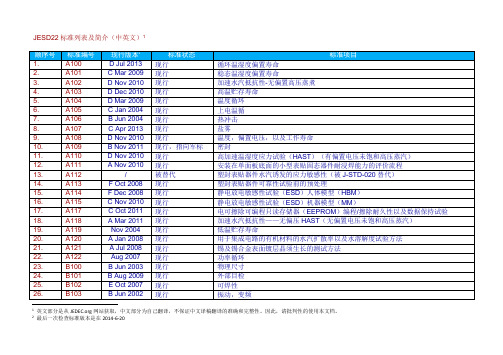
现行
半导体晶圆以及芯片背面外目检
42.
C100
/
已废止
高温连续性
43.
C101
F Oct 2013
现行
静电放电敏感性试验(ESD)场诱导带电器件模型
JESD22-B
Published:Sep-2000Superseded
SUPERSEDEDBYTHETESTMETHODSINDICATEDBY'JESD22-'
JESD22-A100C
Published:Oct-2007
CYCLEDTEMPERATUREHUMIDITYBIASLIFETEST:
TheCycledTemperature-humidity-biasLifeTestisperformedforthepurposeofevaluatingthereliabilityofnonhermeticpackagedsolidstatedevicesinhumidenvironments.Itemploysconditionsoftemperaturecycling,humidity,andbiasthatacceleratethepenetrationofmoisturethroughtheexternalprotectivematerial(encapsulateorseal)oralongtheinterfacebetweentheexternalprotectivematerialandthemetallicconductorsthatpassthroughit.TheCycledTemperature-Humidity-BiasLifeTestistypicallyperformedoncavitypackages(e.g.,MQUADs,liddedceramicpingridarrays,etc.)asanalternativetoJESD22-A101orJESD22-A110.
- 1、下载文档前请自行甄别文档内容的完整性,平台不提供额外的编辑、内容补充、找答案等附加服务。
- 2、"仅部分预览"的文档,不可在线预览部分如存在完整性等问题,可反馈申请退款(可完整预览的文档不适用该条件!)。
- 3、如文档侵犯您的权益,请联系客服反馈,我们会尽快为您处理(人工客服工作时间:9:00-18:30)。
JEDEC standards and publications are adopted without regard to whether or not their adoption may involve patents or articles, materials, or processes. By such action JEDEC does not assume any liability to any patent owner, nor does it assume any obligation whatever to parties adopting
charge for or resell the resulting material.
PRICE: Please refer to the current Catalog of JEDEC Engineering Standards and Publications online at
No claims to be in conformance with this standard may be made unless all requirements stated in the standard are met.
Inquiries, comments, and suggestions relative to the content of this JEDEC standard or publication should be addressed to JEDEC at the address below, or call (703) 907-7559 or
Published by ©JEDEC Solid State Technology Association 2006
2500 Wilson Boulevard Arlington, VA 22201-3834
This document may be downloaded free of charge; however JEDEC retains the copyright on this material. By downloading this file the individual agrees not to
the JEDEC standards or publications.
The information included in JEDEC standards and publications represents a sound approach to product specification and application, principally from the solid state device manufacturer
JEDEC STANDARD
Solder Ball Shear
JESD22-B117, July 2000) OCTOBER 2006
JEDEC SOLID STATE TECHNOLOGY ASSOCIATION
NOTICE
JEDEC standards and publications contain material that has been prepared, reviewed, and approved through the JEDEC Board of Directors level and subsequently reviewed and approved
by the JEDEC legal counsel.
JEDEC standards and publications are designed to serve the public interest through eliminating misunderstandings between manufacturers and purchasers, facilitating interchangeability and improvement of products, and assisting the purchaser in selecting and obtaining with minimum delay the proper product for use by those other than JEDEC members, whether the standard is to
reproduced without permission.
Organizations may obtain permission to reproduce a limited number of copies through entering into a license agreement. For information, contact:
viewpoint. Within the JEDEC organization there are procedures whereby a JEDEC standard or publication may be further processed and ultimately become an ANSI standard.
JEDEC Solid State Technology Association 2500 Wilson Boulevard
Printed in the U.S.A. All rights reserved
PLEASE!
DON’T VIOLATE THE LAW!
This document is copyrighted by the JEDEC Solid State Technology Association and may not be