跨阻放大器(TIA )
光模块介绍 简介

按摩对类风湿有效吗文章目录*一、按摩对类风湿有效吗1. 按摩对类风湿有效吗2. 类风湿怎样才能确诊3. 类风湿严重会导致什么后果*二、导致类风湿出现的主要原因*三、类风湿患者什么不能吃呢按摩对类风湿有效吗1、按摩对类风湿有效吗可以先用推、理、揉手法,轻轻按摩,先使患部肌肉松弛,气血畅行;继而使用点、按、捏、拿手法、达到舒筋活络止痛的目的,最后用摇、滚、揉等手法。
每次治疗时间15到30分钟,2到3天一次。
由此可见,按摩对类风湿是有效的。
2、类风湿怎样才能确诊其实现在对于类风湿的检查,一般都是进行对于血象的检查,因为类风湿的发病的过程,一般都是比较慢的,并且如果是比较严重的类风湿的话一般都是会出现比较轻的中度的贫血,如果是活动期的话一般病人还会出现血小板的增高。
并且如果是比较严重的类风湿的话,还有可能还会有一些人还会出现全部血细胞的减少,其实对于类风湿的确诊的方法还可以做血沉和C反应蛋白的检查,类风湿关节活动期,并且血沈加快。
3、类风湿严重会导致什么后果类风湿连累人的关节主要是表现出类风湿性关节炎,发病的具体部位是关节滑膜,并且还会进一步连累到关节软骨,会使得关节的骨质遭到破坏,最后使得关节发生畸形。
类风湿如果不积极治疗,有75%的人会在发病过后三年左右出现关节残废的现象。
导致类风湿出现的主要原因1、环境因素长期居住在寒冷潮湿环境中的人类风湿的发病率远远高于其它人,类风湿主要是由于外部风邪入侵所致,此外,强烈的精神刺激、外伤、营养不良和过度劳累等都会增加类风湿的发病几率。
2、性激素研究表明,类风湿性关节炎存在明显性别差异,男女发病比例越为1:3,且女性患者在妊娠期症状减轻,服用避孕药的女性较少患病,因此认为性激素在类风湿的产生过程中起到了一定作用。
3、内分泌因素类风湿多发生于女性,患者在怀孕期间症状有所减轻,应用肾上腺皮质激素可以抑制该病,因此推断类风湿的发生于内分泌因素存在关系。
4、免疫因素类风湿的产生是由于感染原侵入关节腔,刺激滑膜或者浆细胞,从而产生特异性免疫球蛋白抗体,当抗原抗体复合物形成后抗体就会转化为异体,再次刺激浆细胞就会产生新的抗体,即类风湿因子,从而导致类风湿发生。
跨阻型放大器应用中关注的指标

跨阻型放大器应用中关注的指标1 引言TIA 全称为trans-impedance amplifier. 也就是跨阻型放大器。
在需要电流转电压的应用场合,如检测微弱光电流信号的场合,通常需要用到跨阻型放大器。
TI有一系列的跨阻放大器,如OPA656,OPA657,OPA843,OPA84,LMH6629 等等。
TI 该产品系列主要的优势在于低噪声,能支持反馈高增益下宽带应用。
这些特点在微弱光检测的场合是非常关键的。
另外TI 的产品是一系列的,在不同的指标要求如带宽升级时可以很方便地找到pin-pin 兼容的产品。
本文介绍了高速TIA 应用中关注的指标及计算过程。
另外介绍了在光检测应用下常见问题的解决。
2 TIA 应用概论在TIA 应用时,由于输入信号是电流,能够应用于这种场合的跨阻放大通常需要具备较低的电流噪声和电压噪声。
比较典型的两个器件是:OPA657(1.6GHz,输入电流噪声1.8 fA/rtHz, 输入电压噪声4.8nV/rtHz),OPA847(3.9GHz, 输入电流噪声2.5pA/rtHz, 输入电压噪声0.85nV/rtHz)。
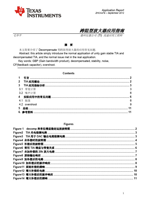
这两款都是Decompensated 放大器。
Decompensated 放大器特点如下:Decompensated 放大器指的是非单位增益稳定的放大器,如OPA657 最小稳定增益是7V/V,OPA847 则为12V/V.其波特图和普通放大器比较如下:和单位稳定放大器相比,其特点如下:带宽更宽,尤其是小信号下的带宽更宽,Slew rate 更快,以及更大的GBW. 另外一般来讲,decompensated 的放大器能够提供更好的电压噪声。
所以在大增益的跨阻放大且要求一定带宽的场合,使用decompensated 放大器要比单位增益稳定放大器有优势。
3 TIA 应用指标分析3.1 带宽计算一个用于光电流检测的常规的跨阻型运放的工作电路一般简化如Figure2 TIA 光电检测电路。
TI跨阻型放大器应用指南
Application ReportZHCA479 – September 2012 1跨阻型放大器应用指南毛华平德州仪器公司 (TI) 高速应用工程师摘 要本文简要介绍了Decompensate 型跨阻型放大器的应用常见问题.Abstract: this article simply introduce the normal application of unity gain stable TIA anddecompensated TIA, and the normal issue met in the real application.Key words: GBP (Gain bandwidth product), decompensated, stability, noise,CF(feedback capacitor), overshoot.Contents1 引言 (2)2 TIA 应用概论 (2)3 TIA 应用指标分析 (3)3.1 带宽计算 33.2 噪声计算 64 实际应用中的常见问题 (6)4.1 振荡 64.2 overshoot 95 总结 (11)6. 参考资料 (11)FiguresFigure 1 decomp 和单位增益稳定运放波特图 (2)Figure2 TIA 光电检测电路 (3)Figure3 TIA 用于DAC 输出电流检测电路 (3)Figure4 未补偿时的波特图 (4)Figure5 补偿后的波特图 (5)Figure6 常用TIA 增益与带宽关系 (6)Figure7 未加补偿的20k 放大电路 (7)Figure8 原始输出响应 (7)Figure9 加补偿后的电路 (8)Figure10 加补偿后的脉冲响应 (8)Figure11 原始补偿的频响 (9)Figure12 增大补偿的电路 (10)Figure13 增大补偿后的脉冲响应 (10)Figure14 增大补偿后的频响 (11)ZHCA4792 跨阻型放大器应用指南1 引言 TIA 全称为trans-impedance amplifier. 也就是跨阻型放大器.在需要电流转电压的应用场合, 如检测微弱光电流信号的场合, 通常需要用到跨阻型放大器. TI 有一系列的跨阻放大器,如OPA656,OPA657,OPA843,OPA84,LMH6629等等. Ti 该产品系列主要的优势在于低噪声, 能支持反馈高增益下宽带应用. 这些特点在微弱光检测的场合是非常关键的. 另外TI 的产品是一系列的, 在不同的指标要求如带宽升级时可以很方便地找到pin-pin 兼容的产品.本文介绍了高速TIA 应用中关注的指标及计算过程. 另外介绍了在光检测应用下常见问题的解决.2 TIA 应用概论在TIA 应用时, 由于输入信号是电流, 能够应用于这种场合的跨阻放大通常需要具备较低的电流噪声和电压噪声. 比较典型的两个器件是:OPA657(1.6GHz,输入电流噪声1.8 fA/rtHz, 输入电压噪声4.8nV/rtHz), OPA847(3.9GHz, 输入电流噪声2.5pA/rtHz, 输入电压噪声0.85nV/rtHz). 这两款都是Decompensated 放大器.Decompensated 放大器特点如下:Decompensated 放大器指的是非单位增益稳定的放大器, 如OPA657最小稳定增益是7V/V , OPA847则为12V/V.其波特图和普通放大器比较如下:Figure 1 decomp 和单位增益稳定运放波特图和单位稳定放大器相比, 其特点如下:带宽更宽, 尤其是小信号下的带宽更宽, Slew rate 更快, 以及更大的GBW. 另外一般来讲, decompensated 的放大器能够提供更好的电压噪声.所以在大增益的跨阻放大且要求一定带宽的场合, 使用decompensated 放大器要比单位增益稳定放大器有优势.G AZHCA479跨阻型放大器应用指南 33 TIA 应用指标分析3.1 带宽计算 一个用于光电流检测的常规的跨阻型运放的工作电路一般简化如下:Figure2 TIA 光电检测电路或是用于作DAC 的电流转电压的应用场合:Figure3 TIA 用于DAC 输出电流检测电路对一定的运放, 其GBP 是固定的, Cdiff(芯片输入的寄生差分容值), Ccm(芯片输入的寄生共模容值)也是固定的, 选定前面的光检测管APD 或PIN 后,其寄生容值CD 也就是固定了, 当放大倍数RF 固定的时候, 其能达到的-3dB 闭环带宽大约为:ZHCA4794 跨阻型放大器应用指南公式1但是由于前端的寄生电容Cs 和Rf 会在噪声增益曲线上形成一个零点,导致运放的开环增益曲线和噪声增益曲线相交处的逼近速度为-40dB/dec, 这样就会造成运放的不稳定,也就是会引起自激. 其波特图如下:Figure4 未补偿时的波特图所以要达到这样一个稳定工作有一个前提, 需要采用CF 来作补偿, 在该曲线中引入一个极点. 补偿后的曲线如下:ZHCA479跨阻型放大器应用指南 5Figure5 补偿后的波特图所以需要让运放稳定工作, 且达到最宽的2阶butterworth 频响, 其CF 的取值如下:公式2对于decompensated 的运放, 由于其最小增益的要求, 还引来另外一个要求, 就是其增益要大于其最小稳定增益, 由于在高频下, 其增益表达式如下:所以对特定的decompensated 的运放, 这个值要大于其最小增益要求.公式3在一个假定前端的寄生容性为10pF 的场合, 以下是几个运放能达到的带宽和增益的对应关系:ZHCA4796 跨阻型放大器应用指南Figure6 常用TIA 增益与带宽关系3.2 噪声计算在由以上公式算出的带宽后, 运放本身带来的噪声贡献可以由如下公式算出:公式4其中:I EQ = 等效的输入噪声电流, 这个值在带宽 F < 1/(2πR F C F )内有效.I N = 运放本身输入的电流噪声,算inverting 的输入.E N = 运放输入的电压噪声.C D = 前面的光电二极管的寄生电容.F = 带宽,单位为Hz.4kT = 1.6E – 21J at T = 290°K 根据这个公式计算出等效的输入噪声电流后, 就可以算出在TIA 输出后SNR 了.4 实际应用中的常见问题这里整理几个TIA 运放在实际使用中经常遇到的问题:4.1 振荡这个问题在高增益,又有宽带要求的情况下比较常见.比如设计一个20K 增益的放大链路, 假设总的输入的寄生电容很大, 10pF. 根据上面的图可以看出, 采用GBW 最宽的OPA847进行设计, 最宽稳定带宽只能在50M 附近.设计电路如下:ZHCA479跨阻型放大器应用指南7Figure7 未加补偿的20k 放大电路输入20n 的脉宽信号, 10u 的幅度, 得到的波形如下:Figure8 原始输出响应输出有振荡产生.根据公式算出CF 的取值应该为0.24p. 加上后,电路如下:ZHCA4798 跨阻型放大器应用指南Figure9 加补偿后的电路仿真得到: 可以看到, 振荡消失,只剩过冲. 放大倍数也趋向正常.Figure10 加补偿后的脉冲响应在高增益的场合, 有可能反馈电阻自带的电容以及反馈走线带来的寄生电容都可以达到这么微小的电容值. 所以需要依具体的测试结果来确定反馈是否要另外加电容.ZHCA479跨阻型放大器应用指南94.2 overshoot在光时域反射检测光纤状态的场合, 输出上的overshoot 可能会对测量结果产生很大影响,这就需要尽可能地减小TIA 输出的overshoot. 如上图所示的结果, 约有10%的overshoot, 这对实际使用是不利的,需要消除.消除这种过冲最有效的方法是加大反馈电容, 但是这样带来的一个直接后果是带宽减小. 如上面的案例, 在输出有overshoot 的情况下, 原始频响为: -3dB 带宽有40M 左右.Figure11 原始补偿的频响增大反馈到0.45p 时, 过冲消失.ZHCA47910 跨阻型放大器应用指南Figure12 增大补偿的电路Figure13 增大补偿后的脉冲响应但是也可以看到, 20nS的脉冲情况下, 其输出有点被滤除, 增益减小了. 原因就在于输出的带宽变窄, 只剩21MZHCA479跨阻型放大器应用指南 11Figure14 增大补偿后的频响5 总结TIA 运放在作电流放大使用时需要注意带宽和增益的折中, 以及平衡性和带宽的折中. 而同时又得兼顾噪声的贡献, 所以需要综合考虑以上的各项指标.6. 参考资料1. Xavier Ramus “Transimpedance Considerations for High-Speed Amplifiers”2. OPA847,OPA657指标书重要声明德州仪器(TI)及其下属子公司有权在不事先通知的情况下,随时对所提供的产品和服务进行更正、修改、增强、改进或其它更改,并有权随时中止提供任何产品和服务。
tia跨阻放大电路
tia跨阻放大电路摘要:1.TIA 跨阻放大电路的概述2.TIA 跨阻放大电路的工作原理3.TIA 跨阻放大电路的应用领域4.TIA 跨阻放大电路的优点与局限性正文:1.TIA 跨阻放大电路的概述TIA 跨阻放大电路,全称为Transimpedance Amplifier,即跨阻抗放大器,是一种常用于信号处理领域的模拟电路。
它具有很高的输入阻抗和很低的输出阻抗,能够将信号源的电流放大并转换为电压信号,从而实现信号的传输和处理。
2.TIA 跨阻放大电路的工作原理TIA 跨阻放大电路的工作原理主要基于运算放大器的运算原理。
运算放大器具有开环增益无穷大、输入阻抗无穷大、输出阻抗零的特点。
在TIA 电路中,运算放大器的非反相输入端接信号源,反相输入端通过电阻网络形成负反馈,使得电路的输出阻抗接近于零。
这样,信号源的电流被放大并转换为电压信号,从而实现信号的传输和处理。
3.TIA 跨阻放大电路的应用领域TIA 跨阻放大电路广泛应用于各种信号处理系统中,如通信系统、仪器仪表、生物医学工程等。
例如,在光纤通信系统中,TIA 跨阻放大电路用于将光信号转换为电信号;在生物医学工程中,TIA 跨阻放大电路可用于生物传感器的信号处理,实现对生物信号的检测和分析。
4.TIA 跨阻放大电路的优点与局限性TIA 跨阻放大电路具有以下优点:(1)高输入阻抗:TIA 电路的输入阻抗很高,可以最大程度地保留信号源的特性,避免信号衰减或失真。
(2)低输出阻抗:TIA 电路的输出阻抗接近于零,能够驱动较大的负载电阻,实现信号的有效传输。
(3)宽频带:TIA 电路具有较宽的频带,能够处理不同频率范围的信号。
然而,TIA 跨阻放大电路也存在一定的局限性:(1)对运算放大器的依赖性:TIA 电路的工作原理基于运算放大器,因此,运算放大器的性能直接影响TIA 电路的性能。
(2)稳定性:TIA 电路的稳定性受负反馈网络的影响,如果设计不当,可能导致电路不稳定。
电力通信常用英文缩写及名词解析
常用英文缩写名词解析AAC:Alternating Current 交流电流AAU:Active Antenna Unit 有源天线单元ASE:Amplified Spontaneous Emission 放大自发辐射(光源)AOC:Active Optical Cable 有源光缆APD:Avalanche Photo Diode 雪崩光电二极管APC:Automatic Power Control 自动功率控制ACC:Automatic Current Control 自动电流控制AGC:Automatic Gain Control 自动增益控制APR:Automatic Power Reduction 自动功率减小ASON:Automatically Switched Optical Network 智能光网络AMP::Asynchronous Mapping Procedure 异步映射规程BBBU:Building Base band Unite 基带处理单元BOL:Begin Of Life 额定电流BiDi:Bi-Directional 单纤双向BMP:Bit-synchronous Mapping Procedure 比特同步映射规程CC-RAN:Centralized Radio Access Network 集中化无线接入网CU:Centralized Unit 集中单元CoMP:Coordinated Multiple Points Transmission/Reception多点协作传输CO:Central Office 中心机房CD:Chromatic Dispersion 色度色散CDR:Committed Data Rate 承诺数据速率CATV:Cable Television 有线电视网CFP:外形封装可插拔模块CXP:十二路小型可插拔模块DDU: Distribute Unit 分布单元DSP:Digital Signal Processing 数字信号处理DSF:Dispersion Shifted Fiber 色散位移光纤DC:Direct Current 直流电流DCF:Dispersion Compensating Fiber色散补偿光纤(光纤型色散补偿设备)DCI:Data Center Interconnection 数据中心互联DFB:Distributed Feedback Laser 分布式反馈激光器DCN:Data Communication Network 数据通信网络EEMI:Electromagnetic Interference 电磁干扰EPON:Ethernet Passive Optical Network 以太网无源光网络ESD:Electro-Static Discharge 静电释放EAM:Electro Absorption Modulator 电吸收调制器EML:EAM Laser 电吸收调制激光器ESC:Electrical Supervisory Channel 电监控信道FFWM:Four-Wave Mixing 四波混频FGA:Fixed Gain Gmplifier 固定增益放大器FBG:Fiber Bragg Grating Sensor光纤布拉格光栅传感器(光栅型色散补偿设备)FAN:散热风扇面板FEC:Forward Error Correction 前向纠错FP-LD:Fabry-Perot Laser 法布里-珀罗激光器FTTx:Fiber To The x 光纤到xFTTH:光纤到户FTTB:光纤到楼FTTCab:光纤到交接箱FTTC:光纤到路边FTTD:光纤到桌面FTTP:光纤到驻地FTTO:光纤到办公室FTTu:光纤到用户FIU:Facilities Interface Unit 设备接口单元GPIB:General-Purpose Interface Bus 通用接口总线GPON:Gigabit-Capable Passive Optical Networks吉比特无源光网络(千兆无源光网络)GFF:Gain Flatness Filter 增益平坦滤波器GMP:Generic Mapping Procedure 通用映射规程IITU:International Telecommunication Union 国际电信联盟ILA:光线路中继器IL:Insertion Loss 插入损耗ITL:Interested Transaction List 传输槽位(事务槽)LLD:Laser Diode 激光二极管LAN:Local Area Network 局域网MMux/DEMux:Multiplexing/demultiplexing 复用/解复用MLM:Multi-Longitudinal Mode 多纵模MP:网管控制设备MT-RJ:multi transmit receive joint 多芯收发一体方型接头MPO:Multi-fiber Push On 多芯多通道光纤跳线MPD:Monitoring Photo Diode 监控光电二极管NFV:Network Function Virtualization 网元虚拟化OOSNR:Optical Signal Noise Ratio 光信噪比OSA:OpticalSpectrum Analysis 光谱分析仪ODF:Optical Distribution Frame 光纤配线架OTDR:Optical Time Domain Reflector 光时域反射器OMT:Optical multiplexing terminal 光复用终端OTN:Optical Transport Network 光传输网OLP:Optical Fiber Line Auto Switch Protection Equipment光纤线路自动切换保护装置OEO:Optical-Electrical-Optical 光电光OMU:Optical Multiplex Unit 光合波单元(光复用单元)ODU:Optical Demultiplexing Unit 光分波单元OSA:Optical Subassembly 光学次模块(光学组件)BOSA:Bi-direction Optical Subassembly 光收发模块ROSA:Receiver Optical Subassembly 光接收模块TOSA:Transmitter Optical Subassembly 光发送模块ONT:Optical Network Terminal 光网络终端ONU:Optical Network Unit 光网络单元OLT:Optical Line Terminal 光线路终端OTM:Optical Termination Multiplexer 光终端复用器OSC:Optical Supervisory Channel 光监控信道OLA:Optical Line Amplifier 光线路放大器OADM:Optical Add Drop Multiplexer 光分插复用设备OTU:Optical Transform Unit 光波长转换器(光转换单元)ODU:Optical channel Date Unit 光通道数字单元ODUflex:灵活速率光通信单元OTS:Optical Transmission Section 光传输段OMS:Optical Multiplex Section 光复用段OCH:Optical Channel 光通道PPTU:Power Transfer Unit 电源开关PSM:Pulse Step Modulation 脉冲波形调制PWR:电源设备PMD:Polarization Mode Dispersion 偏振模色散PSM:Parallel Single Mode 平行单模PCB:Printed Circuit Board 印刷电路板PDL:Polarization Dependent Loss 偏振相关损耗PTN:Packet Transport Network 分组传送网PIN:PIN型光电二极管QQSFP:Quad Small Form-factor Pluggable 四通道小型可插拔模块RRRU:Remote Radio Unit 射频拉远单元RFI:Radio Frequency Interference 射频干扰RS-232:recommended Standard-232 串行中心接口标准REG:Regenerator Station 中继站SSTM;Synchronous Transfer Module 同步传输模式STM-1:传输速率为155.520MbpsSTM-4:传输速率为622.080MbpsSTM-16:传输速率为2.488GbpsSTM-64:传输速率为10GbpsSMF:System Management Facilities 系统管理程式SDH:Synchronous Digital Hierarchy 同步数字体系SER:Symbol Error Rate 误码率SPM:Self-Phase Modulation 自相位调制SRS:Stimulated Raman Scattering 受激拉曼散射SLM:Single-Longitudinal Mode 单纵模3R:Signal Reshaping 信号再整形Signal Reamplification 信号再放大Signal Retiming 信号重新定时SBS:Stimulated Brillouin Scattering 受激布里渊散射SLED:Super Luminescent Diode 超辐射发光二极管SFP:Small Form-factor Pluggable 小型可热插拔光模块SONET:Synchronous Optical Network 同步光纤网络SFF:Small Form Factor 小型化光纤连接器件TTDM:Time Division Multiplexing 时分复用TLS:Tunable Laser Source 可调谐激光光源TAP:Test Access Point 网络分路器TO:Transistor Outline 晶体管外形封装TEC:Thermo Electric Cooler 半导体制冷器TIA:Trans-Impedance Amplifier 传输阻抗放大器(跨阻放大器)VVM:Virtual Machine 虚拟机VGA:Variable Gain Amplifier 可变增益放大器VCSEL:Vertical Cavity Surface Emitting Laser垂直腔面发射激光器VPWS:Virtual Private Wire Service 虚拟专用线服务WWDL:Wavelength Dependent Loss 波长相关损耗XXPM:Cross-Phase Modulation 交叉相位调制xPON:Passive Optical Network 无源光网络放大器OA:Optical Amplifier 光放大器EDFA:Erbium-Doped Fiber Amplifier 掺铒光纤放大器DRA:Distributed Raman Amplifier 分布式拉曼放大器EYDFA:Erbium-Yterbium-Doped Fiber Amplifier铒镱共掺光纤放大器SOA:Semiconductor Optical Amplifier 半导体光放大器复用方式CDM:Code Division Multiplex 码分复用FDM:Frequency Division Multiplex 频分复用TDM:Time Division Multiplex 时分复用WDM:Wavelength Division Multiplex 波分复用CWDM:Coarse Wavelength Division Multiplex 粗波分复用DWDM:Dense Wavelength Division Multiplex 密集波分复用泵浦模式SF:Same-fiber Forward 同一光纤前向DB:Different-fiber Backward 不同光纤后向SB:Same-fiber Backward 同一光纤后向DF:Different-fiber Forward 不同光纤前向波长单模光纤的传输带宽为1260nm至1675nm,共415nm宽度。
MSP430FR2311智能模拟组合和跨阻放大器使用指南说明书
Application ReportSLAA705A–July2016–Revised November2019How to Use the Smart Analog Combo and Transimpedance Amplifier on MSP430FR2311ABSTRACTIn sensing applications,operational amplifiers are often needed to condition(for example,to amplify and filter)the analog sensor output so that it can be properly sampled by the analog-to-digital converter(ADC) on the microcontroller(MCU).This application report provides a guide to set up the integrated operational amplifiers(TIA and SAC_OA)on the MSP430FR2311MCU.Examples are provided for using the integrated operational amplifiers as a transimpedance amplifier for current sensing applications.Considerations for low-power operation are also discussed.Contents1Introduction (2)2Configuration of the Integrated Operational Amplifiers (3)2.1Configuration of SAC_OA (3)2.2Configuration of TIA (4)3Application Examples (5)3.1SAC_OA as a Transimpedance Amplifier (5)3.2TIA Module as a Transimpedance Amplifier (7)3.3A Current Sensing System Demo (8)4References (10)List of Figures1SAC_OA Block Diagram (3)2SAC0OA Register(Address0x0C80) (3)3P1SEL0Register(Address0x020A) (4)4P1SEL1Register(Address0x020C) (4)5TIA Block Diagram (4)6TRICTL Register(Address0x0F00) (5)7Transimpedance Amplifier With SAC_OA (6)8Output Voltage With1-µA Input Current (6)9Output Voltage With50-nA Input Current (7)10Transimpedance Amplifier With TIA (7)11Output Voltage With1-µA Input Current (8)12Block Diagram of the Out-of-Box Demo (8)13Output Voltage When the Op Amp is Dynamically Turned On and Off (9)14Power Consumption of the Out-of-Box Demo (9)TrademarksLaunchPad,Code Composer Studio,EnergyTrace are trademarks of Texas Instruments.All other trademarks are the property of their respective owners.1 SLAA705A–July2016–Revised November2019How to Use the Smart Analog Combo and Transimpedance Amplifier onIntroduction 1IntroductionIn many sensing applications,the raw analog output of a sensor must be amplified,filtered,or converted to a voltage to be properly sampled by the analog-to-digital converter(ADC).The digital stream from the ADC is then processed by an MCU to extract the useful information.One example is a transimpedance amplifier.The transimpedance amplifier converts the output current from a sensor to a voltage that isreadable by an ADC.Stand-alone operational amplifiers(OAs)are normally used to perform the task.To reduce the cost and design complexity,two configurable operational amplifiers are implemented onMSP430FR2311mixed signal microcontroller for single chip designs.This application report describes how to set the MSP430FR2311control registers to use the integrated OAs as general-purpose OAs.The transimpedance amplifier for the current sensing applications is used as examples to demonstrate the operation.One complete current sensing system example is discussed with consideration for low-power applications.The examples are verified with the MSP430FR2311LaunchPad™development kit.The MSP430FR2311includes two integrated OAs:•Transimpedance amplifier(TIA)•General-purpose OA in the Smart Analog Combo module(SAC_OA)There are two major differences between those two OA modules.The first difference is the input biascurrent.On the TSSOP16package,there is a dedicated pin for the negative input of the TIA module,and the input bias current is much lower compared to input pins that are multiplexed with other functions.The second difference is input voltage range.The inputs of the TIA module support only half-rail voltage,while the inputs of the SAC_OA module support rail-to-rail voltage.In applications that require wider bandwidth,a second stage of OA is required.The integrated OAs on the MSP430FR2311make design simple with the internal connections between the two OAs and ADC.The user can choose the TIA module for the first stage and the SAC_OA as the second stage.The TIA output is internally connected to the SAC_OA input.The SAC_OA output is internally connected to the ADCinput.No external connection is needed,which not only reduces cost but also improves signal quality.Although the OA outputs are internally connected to next stage of processing,they must be routed to the external pins because the external feedback network is required.The electrical characteristics of the integrated OAs can be found in the MSP430FR2311data sheet.For more details about how to design with operational amplifiers,refer to the following application reports: An Applications Guide for Op AmpsHandbook of Operational Amplifier ApplicationsFor more details about transimpedance amplifiers,refer to the following application reports:Transimpedance Amplifiers(TIA):Choosing the Best Amplifier for the JobTransimpedance Considerations for High-Speed Operational AmplifiersThe user must verify the sensor specifications and working conditions for application so that the integrated OAs are configured properly.OA0O (P1.3)COMPADCOA0- (P1.2)Reserved ReservedOA0+ (P1.4)TRI0OReserved 3SLAA705A–July 2016–Revised November 2019How to Use the Smart Analog Combo and Transimpedance Amplifier on2Configuration of the Integrated Operational AmplifiersThis section describes how to set up the MSP430FR2311control registers to enable the integrated operational amplifiers as general-purpose operational amplifiers.There are two steps in setting up an integrated OA to work as a general-purpose OA.•Enable and configure the OA module.•Configure the pin multiplexing to enable required OA functions on the external pins.2.1Configuration of SAC_OAFigure 1shows the block diagram of SAC_OA.The black squares are the control bits in the SAC0OA register.In addition to an external pin,the output of the SAC_OA is internally connected to inputs of the compare (eCOMP)and analog-to-digital converter (ADC)modules for further processing.The internal connections save pins so that signal is not routed out and then back into the device,which also can be advantageous in respect to noise.The control registers of the eCOMP and ADC modules must be configured to use this signal as input.Figure 1.SAC_OA Block DiagramTo enable SAC_OA as a general-purpose operational amplifier,the OAEN,PMUXEN,and NMUXEN bits must be set in the SAC0OA register.Configure the OAPM bit to select high-speed or low-speed mode according to the application requirements.The high-speed mode enables faster slew rate at the cost of higher power consumption.The PSEL bits can be configured to connect the positive input to the external pin or TIA output.Figure 2shows the definition of the control register SAC0OA.For example,a value of 0x0588must be written to the SAC0OA register to set up SAC_OA inputs to external pins and set SAC_OA in low-power low-speed mode.15141312111098ReservedSACEN OAPM OAEN r0r0r0r0r0rw-(0)rw-(0)rw-(0)7654321NMUXEN ReservedNSELPMUXEN ReservedPSELrw-(0)r0rw-(0)rw-(0)rw-(0)r0rw-(0)rw-(0)Figure 2.SAC0OA Register (Address 0x0C80)The I/O pins on MSP430FR2311are multiplexed with multiple module functions.The GPIO port control registers P1SEL0and P1SEL1must be configured to enable the SAC_OA function on the external pins.Figure 3and Figure 4show the definition of the P1SEL0and P1SEL1registers,respectively.Bits 2,3,and 4must be set in both the P1SEL0and P1SEL1registers to enable operational amplifier function on the external I/O pins.TRI0- (P1.6)TRI0O (P1.5)OPA0+COMPADCTRI0+ (1.7)Reserved Reserved Reserved76543210P1SEL0rw-0rw-0rw-0rw-0rw-0rw-0rw-0rw-0Figure 3.P1SEL0Register (Address 0x020A)7654321P1SEL1rw-0rw-0rw-0rw-0rw-0rw-0rw-0rw-0Figure 4.P1SEL1Register (Address 0x020C)As an example,use the code sequence in Example 1to enable SAC_OA in low-speed mode with MSPWare driverlib APIs.In this example,all SAC_OA pins are routed to external I/O pins.Example 1.Code Example for Configuring SAC_OA//Enable op amp functions on external pinsGPIO_setAsPeripheralModuleFunctionInputPin (GPIO_PORT_P1,GPIO_PIN2|GPIO_PIN3|GPIO_PIN4,GPIO_TERNARY_MODULE_FUNCTION);//Select external pins for both positive and negative inputs SAC_OA_init(SAC0_BASE,SAC_OA_POSITIVE_INPUT_SOURCE_EXTERNAL,SAC_OA_NEGATIVE_INPUT_SOURCE_EXTERNAL);//Select low speed and low power modeSAC_OA_selectPowerMode(SAC0_BASE,SAC_OA_POWER_MODE_LOW_SPEED_LOW_POWER);//Enable OASAC_OA_enable(SAC0_BASE);//Enable SACSAC_enable(SAC0_BASE);2.2Configuration of TIAFigure 5shows the block diagram of the TIA module.The black squares are the control bits in the TRICTL register.In addition to an external pin,the output of TIA is internally connected to inputs of the eCOMP,ADC,and SAC_OA modules for further processing.The control registers of those modules must be configured to use this signal as input.Figure 5.TIA Block Diagram Application Examples5SLAA705A–July 2016–Revised November 2019How to Use the Smart Analog Combo and Transimpedance Amplifier onTo enable TIA as a general-purpose operational amplifier,the TRIEN bit must be set in the TRICTL register.Configure the TRIPM bit to select high-speed or low-speed mode.A value of 0x01must be written to the TRICTL register to enable TIA as a general-purpose operational amplifier in low-speed mode.To support faster slew rate,the high-speed mode can be set by writing a value of 0x3to theTRICTL register.The high-speed mode consumes more power than the low-speed mode.Figure 6shows the definition of the TRICTL register.15141312111098Reserved r-0r-0r-0r-0r-0r-0r-0r-076543210TRIPSELReservedTRIPM TRIEN rw-(0)rw-(0)r-0r-0r-0r-(0)rw-(0)rw-(0)Figure 6.TRICTL Register (Address 0x0F00)The GPIO port control register P1SEL0and P1SEL1must be configured to enable the TIA function on the external pins.Bits 5,6,and 7must be set in both P1SEL0and P1SEL1registers to enable the TIA function on the external I/O pins.As an example,the code sequence in Example 2can be used to set up TIA in low-speed mode with MSPWare driverlib APIs.Example 2.Code Example for Configuring TIA//Configure Op-Amp functionality for the external pins GPIO_setAsPeripheralModuleFunctionInputPin(GPIO_PORT_P1,GPIO_PIN5|GPIO_PIN6|GPIO_PIN7,GPIO_TERNARY_MODULE_FUNCTION);//Select low power low speed modeTRI_selectPowerMode(TRI0_BASE,TRI_LOW_SPEED_LOW_POWER);//Enable TIATRI_enable(TRI0_BASE);3Application ExamplesWhen an integrated OAs is enabled and signals are routed to external I/O pins,the module can be used as a stand-alone OA.The functionality of the amplifier is determined by the feedback network.The following examples are based on the circuit of the MSP430FR2311LaunchPad development kit.3.1SAC_OA as a Transimpedance AmplifierIn many applications,the sensing element (a photodiode,for example)is a current source.Atransimpedance amplifier is required to convert the sensor output current to voltage so that it can be read by the ADC module.A transimpedance amplifier composed of the SAC_OA module (see Figure 7).Application Examples Figure7.Transimpedance Amplifier With SAC_OAThe gain of the transimpedance amplifier is purely determined by the value of the feedback resistor when the input bias current of the operational amplifier is negligible.For the circuit in Figure8,a voltage of2.5V is observed at the OA0O pin when the photodiode generates an output of1µA.The1-pF bypasscapacitor enables a low-pass filter with a pole at63kHz to eliminate potential oscillation at highfrequencies.Figure8shows the op amp output voltage with1-µA input current.For this example,the photodiode on the MSP430FR2311LaunchPad development kit is replaced by a current source.The current source is constructed by a function generator with a1-MΩresistor in series.Figure9shows the op amp outputvoltage with50-nA input current.The input waveform is on Channel2,and the output is on Channel1. ArrayFigure8.Output Voltage With1-µA Input CurrentTRI0O (P1.5) Application Examples7 SLAA705A–July2016–Revised November2019How to Use the Smart Analog Combo and Transimpedance Amplifier onFigure9.Output Voltage With50-nA Input Current3.2TIA Module as a Transimpedance AmplifierThe transimpedance amplifier in Figure10is the same as in Figure7except that the operational amplifier is replaced by the TIA module.On the TSSOP16package,the TIA module is the preferred choice for a transimpedance amplifier due to the small input bias current on the TRI0-pin.A user can take advantage of the low input bias current when interfacing a sensor with low output current.Figure10.Transimpedance Amplifier With TIAFigure11shows the output voltage with1-µA input current pulses.On the MSP430FR2311LaunchPad, the phot diode is replaced by a current source.Jumpers are removed to disconnect the SAC_OA pinsfrom input.Then two jumper wires are used to connect the feedback resistor and current source to the TIA negative input and output.The TIA positive input is tied to ground via a jumper wire.The noise level is high in the output due to long jumper wires.In a real application,the signal traces to the op amp must be as short as possible to minimize noise.PhotodiodeApplication Examples Figure11.Output Voltage With1-µA Input Current3.3A Current Sensing System DemoThe out-of-box demo provided with the MSP430FR2311LaunchPad development kit implements acomplete current sensing system example.It shows how to use the integrated op-amp(SAC_OA)as a transimpedance amplifier along with the timer,ADC,and external LED to implement a light sensor forultra-low-power applications.Figure12shows the block diagram of the demo.The transimpedance amplifier is made of the SAC_OA module.It converts the current from the photodiode to a voltage.1-µA input current produces a voltage of2.5V.This voltage is then read by the analog-to-digital converter(ADC)and fed to a timer module to drivean external LED with PWM.The duty cycle of the PWM is proportional to the current from the photodiode.As more light reaches the photodiode,the LED becomes brighter.Figure12.Block Diagram of the Out-of-Box DemoTo demonstrate how to reduce power consumption,the device is kept in lower-power mode most of time.A timer is set up to wake up the device every50ms for the measurements.The complete CodeComposer Studio™IDE project for the demo can be downloaded from the TI web site. Application Examples9SLAA705A–July 2016–Revised November 2019How to Use the Smart Analog Combo and Transimpedance Amplifier onFigure 13shows the output voltage of the transimpedance amplifier when it is dynamically enabled and disabled.After the OA is enabled,a small delay is needed before starting the ADC module so that the ADC module does sample the transient pulse when the op amp is enabled.Figure 13.Output Voltage When the Op Amp is Dynamically Turned On and OffFigure 14shows the power consumption of the demo.This data was captured using EnergyTrace™technology.The power profile data indicates a battery life of 380days when a CR2032battery is used.Figure 14.Power Consumption of the Out-of-Box DemoThis demonstration provides functional blocks that can be used for applications such as smoke detectors and gas detectors.References 4References1.MSP430FR231x Mixed-Signal Microcontrollers2.MSP430FR4xx and FR2xx Family User’s Guide3.MSP430FR2311LaunchPad™Development Kit(MSP-EXP430FR2311)User's Guide4.AN-20An Applications Guide for Op Amps5.Handbook of Operational Amplifier Applications6.Transimpedance Amplifier(TIA):Choose the Best Amplifier for the Job7.Transimpedance Considerations for High-Speed Amplifiers Revision History11SLAA705A–July 2016–Revised November 2019Submit Documentation Feedback Copyright ©2016–2019,Texas Instruments IncorporatedRevision History Revision HistoryNOTE:Page numbers for previous revisions may differ from page numbers in the current version.Changes from July 20,2016to November 15,2019Page •Changed the document title;editorial changes in abstract (1)IMPORTANT NOTICE AND DISCLAIMERTI PROVIDES TECHNICAL AND RELIABILITY DATA (INCLUDING DATA SHEETS), DESIGN RESOURCES (INCLUDING REFERENCE DESIGNS), APPLICATION OR OTHER DESIGN ADVICE, WEB TOOLS, SAFETY INFORMATION, AND OTHER RESOURCES “AS IS” AND WITH ALL FAULTS, AND DISCLAIMS ALL WARRANTIES, EXPRESS AND IMPLIED, INCLUDING WITHOUT LIMITATION ANY IMPLIED WARRANTIES OF MERCHANTABILITY, FITNESS FOR A PARTICULAR PURPOSE OR NON-INFRINGEMENT OF THIRD PARTY INTELLECTUAL PROPERTY RIGHTS.These resources are intended for skilled developers designing with TI products. You are solely responsible for (1) selecting the appropriate TI products for your application, (2) designing, validating and testing your application, and (3) ensuring your application meets applicable standards, and any other safety, security, regulatory or other requirements.These resources are subject to change without notice. TI grants you permission to use these resources only for development of an application that uses the TI products described in the resource. Other reproduction and display of these resources is prohibited. No license is granted to any other TI intellectual property right or to any third party intellectual property right. TI disclaims responsibility for, and you will fully indemnify TI and its representatives against, any claims, damages, costs, losses, and liabilities arising out of your use of these resources.TI’s products are provided subject to TI’s Terms of Sale or other applicable terms available either on or provided in conjunction with such TI products. TI’s provision of these resources does not expand or otherwise alter TI’s applicable warranties or warranty disclaimers for TI products.TI objects to and rejects any additional or different terms you may have proposed.Mailing Address: Texas Instruments, Post Office Box 655303, Dallas, Texas 75265Copyright © 2022, Texas Instruments Incorporated。
光模块基本原理 ——解释

光器件结构图
光器件分类
如按功能,可分为:
光发射器件 光接收器件 按结构,可分为: TO器件(TOSA, ROSA,BOSA); DIP(或Butterfly)器件; 表面贴装(surface mount) 器件等; 按传输速率,可分为 155M、622M、1.25G、2.5G、10G等; 传输距离,工作波长,工作方式等
D Flip-Flop
驱动芯片
激光器驱动(电流) 调制器驱动(电压)
MUX &DeMUX
MUX:16路并行 数据输入,经过并串转换,输出数 据。(如并行数据输入为622Mb/s ,那么输出数据为 9.95Gb/s) DeMUX:则反过来,输入数据经过串并转换,输出16 路并行 数据
光模块原理框图
光模块主要性能指标
光模块接口电平
光模块内部主要元器件
探测器
激光器 放大器
时钟数据恢复 驱动芯片 MUX&光电 子元件和IC 、无源元件( 如电阻、电容、电感、互 感、微透镜、隔离器)、 光纤及金属连线组合、封 装在一起,完成单项或少 数几项功能的混合集成件 。
光模块发展历史
封装形式:1X9 SFF GBIC SFP, XFP, SFP+ 传输速率:155M,622M 1.25G,2.5G 4.25G, 8.5G, 10G, 40G 光接口形式:尾纤型(Pigtail);插拔型(Receptacle) 光传输形式:双纤双向(MSA);单纤双向(BiDi)
LOS
数字诊断(DDM)模块特点
光收发合一模块(XFP)功能框图
TxDisable
Data In
CDR
Driver APC/AEC/ATC
电流电压转换器

目录[隐藏]∙ 1 应用∙ 2 原本的概念基础o 2.1 非电气领域:流量产生压力o 2.2 电气域:电压电流的原因o 2.3 无源版本的应用程序▪ 2.3.1 电流到电压转换器作为输出设备▪ 2.3.2 电流到电压转换器作为输入设备▪ 2.3.3 I至V转换为负反馈的V型,电流转换器的一部分o 2.4 非理想无源版本∙ 3 改进:有功电流电压转换器o 3.1 背后的活动版本的基本思路▪ 3.1.1 非电域:卸下相当于“抗干扰”的干扰,▪ 3.1.2 电气域:卸下电压相当于“反电压”o 3.2 运算放大器实现o 3.3 运算放大器电路的操作o 3.4 I-V的转换器与跨阻放大器∙ 4 参见∙ 5 参考资料∙ 6 外部链接应用常用的阻放大器在光通信接收器。
由一个光电探测器所产生的电流产生的电压,但在非线性的方式。
因此放大器具有低输入阻抗,以防止任何大的电压,并产生50欧姆信号(许多人认为,低阻抗)来驱动同轴电缆或电压信号进一步放大。
但要注意,最线性放大是由双极晶体管的电流放大,所以你可能要放大的阻抗转换前。
原本的概念基础非电气领域:流量产生压力在实体方面,有许多情况下压力量诱导通过一个障碍的一种物质流。
然而,也有相应的情况下,数量的流动诱导的障碍压力:机械(如果试图停止与他的身体,“流动的”汽车施加压力,他的障碍的移动车),气动(捏在中间的软管,你会看到一个压在夹点出现)。
在这种安排下,流量,压力,和属性类似的障碍是相互关联的的。
通常情况下,可变输出的压力成正比;这种方式,创建流的数量(转换为输入流,像之一)压力。
诱发的压力,一个障碍,必须在一个流动的数量方式。
[编辑]电气域:电压电流的原因图2。
被动的电流 - 电压的转换器的基础上电流会导致电压的现象。
建立电路。
同样,在电器的领域,如果通过电阻R(图2)流动的电流I,后者阻碍(抵抗)目前,作为一个结果,成比例的V R = RI电阻两端的根据当前出现原因电压制定欧姆定律(V = RI)。
tia跨阻放大电路
TIA跨阻放大电路简介TIA跨阻放大电路(Transimpedance Amplifier)是一种常用于光电探测器中的电路,用于将光电器件输出的电流转换为电压信号。
TIA电路的核心是一个跨阻放大器,它能够将输入的电流信号放大,并转换为输出的电压信号。
TIA跨阻放大电路在光通信、光电测量等领域具有广泛的应用。
TIA跨阻放大器原理TIA跨阻放大器的基本原理是利用负反馈放大器的特性,将输入电流转换为输出电压。
它由一个光电二极管作为输入电流源,一个电阻作为负载,以及一个运算放大器(Operational Amplifier)构成。
TIA电路的输入端连接到光电二极管,当光照射到光电二极管时,产生的光电流会通过输入电阻流入电路。
运算放大器的反向输入端连接到电阻的接地端,形成负反馈回路。
运算放大器的输出端与电阻的另一端相连,输出电压通过反馈电阻回到运算放大器的反向输入端。
当输入电流流入电路时,会在电阻上产生一个电压降,根据欧姆定律,电压与电流成正比。
运算放大器通过负反馈作用,将电阻上的电压放大,并输出到负载上。
TIA跨阻放大器设计要点在设计TIA跨阻放大器时,需要考虑以下几个关键要点:1. 输入电阻选择TIA电路的输入电阻需要足够大,以保证光电二极管输出的电流能够流入电路而不被短路。
一般选择高阻值的电阻,如几兆欧姆,以确保输入电流的有效转换。
2. 反馈电阻选择反馈电阻的选择决定了TIA电路的放大倍数。
一般情况下,反馈电阻越大,放大倍数越高。
但是过大的反馈电阻会引入噪声,影响电路的性能。
因此,需要在放大倍数和噪声之间做出权衡。
3. 运算放大器的选择运算放大器是TIA电路的核心部件,需要选择性能优良的运算放大器。
一般选择带宽较宽、噪声较低的运算放大器,以保证电路的放大性能和稳定性。
4. 功耗和速度考虑TIA电路在应用中还需要考虑功耗和速度的问题。
功耗较高的电路会产生较多的热量,影响电路的稳定性;速度较慢的电路会导致信号延迟,影响系统的响应速度。
跨阻放大器的输入阻抗无穷大还是为零究竟是
跨阻放大器的输入阻抗:无穷大还是为零?究竟是多少?跨阻放大器的输入阻抗:无穷大还是为零?究竟是多少?跨阻放大器(TIA)的输入阻抗是多少呢?无穷大还是零呢?都不是,究竟是多少?没有事物是绝对为零或绝对无穷大的,对吗?即使你没有用过TIA,TIA输入阻抗的值会让你惊讶,值得你去理解。
毕竟,一个反向放大器就是一个有输入电阻的TIA ,对吗?TIA将一个电流信号转换成电压,并且经常用于测量弱电流,。
对于理想运放,有无穷大的开环增益和带宽,输入阻抗为零。
运放的反馈回路使得V1保持虚地,得到一个零输入电阻。
类似一个电流表,一个理想的电流测量电路的输入阻抗应该为零。
我们仍然假设运放工作在理想条件下,但实际上运放的增益带宽积是有限的,我们应该思考其输入阻抗Z是多少?一些推论和8阶的代数式揭示出一个有趣的结果。
图2是OPA314的开环增益随频率变化的曲线。
对于今天的大多数运放,在一个较宽的频率范围内------超过通用器件的50倍,开环增益以一个恒定的斜率-20dB/10倍频下降。
它的增益带宽积是3MHz,所以在这个范围以内的任何频率下,其增益接近3MHz/f。
在黄色方框内标出的因子揭示了结果。
Z和Rf,f成正比,和增益带宽积成反比。
但是,Z和f成正比意味着什么呢?它感觉更像一个基本的电路元件------电感。
一个电感的阻抗是,所以我们可以将TIA的输入端等效为一个电感。
这非常巧,是吗?也许你之前已经知道了这一点。
在一个较宽的频率范围内,输入端可以视为一个电感负载。
在大多数应用中,我们希望这个电感越小越好。
RF通常是根据跨阻增益而定,所以更高的增益带宽积是减小这个电感的唯一方法。
将这种方法应用于实际,你可能会从光电二极管或者电流转换电路中获得更多的洞察力。
没有更多新的东西在这里。
各种使用运放合成的电感电路已经存在了很长一段时间,但是你可能没有将它和TIA或者反向放大器联系起来。
建立这种联系会带来更深层次的思考和创造力。
- 1、下载文档前请自行甄别文档内容的完整性,平台不提供额外的编辑、内容补充、找答案等附加服务。
- 2、"仅部分预览"的文档,不可在线预览部分如存在完整性等问题,可反馈申请退款(可完整预览的文档不适用该条件!)。
- 3、如文档侵犯您的权益,请联系客服反馈,我们会尽快为您处理(人工客服工作时间:9:00-18:30)。
跨阻放大器(TIA )全称为trans-impedance amplifier,是放大器类型的一种,放大器类型是根据其输入输出信号的类型来定义的。
TIA的功能如同我们平时在养花的过程中给花施肥的一样,如果一片贫瘠的土地上要种出鲜艳的花朵,那么在给这片土地施肥的时候,杂草和花苗同样得到了滋养,这时候我们就会人为地将杂草拔掉,这样杂草没了,肥料的营养能最大程度地供养给花苗,然后花苗才能茁壮成长。
TIA在DWDM系统中的作用就相当于我们人为地将杂草拔掉,而且还一定程度上抵制了杂草的重生。
在电学范畴,假设放大器增益A=Y/X,Y为输出,X为输入。
由于表征一个信号不是用电压就是电流,所以组合一下就有4种放大器,当输入为电流信号,输出为电压信号时,A=Y(电压)/X(电流),具有电阻的量纲,所以一般称之为跨阻放大器,另外,我们常见的都是电压放大器,也就是输入输出都是电压的那种。
TIA由于具有高带宽的优点,一般用于高速电路,如光电传输通讯系统中普遍使用。
例如PIN-TIA,PIN-TIA光接收器是用于光通信系统中将微弱的光信号转换成电信号并将信号进行一定强度低噪声放大的探测器件,其工作原理是:PIN的光敏
面受探测光照射时,由于p-n结处于反向偏置,光生载流子在电场的作用下产生漂移,在外电路产生光电流;光电流通过跨阻放大器放大输出,这样就实现了光信号转换成电信号进而将电信号初步放大的功能。
在实际应用中,我们会根据TIA的要求,采用-5.2 V、3.3 V或其它的供电形式,用不同的外围电路形式来完成封装。
我们知道在DWDM系统中,OSNR是衡量整个系统传输性能的重要指标之一,也就是信号和噪声的比值,如何将信噪比提高到一个理想的传输性能值,从上面的描述就可得知引入了TIA,它能将电信号进行一定强度的低噪放大。
信号在经过光纤传输后,光功率和色散必然在一定程度上有所衰减,光放大器将光信号转化为电信号来进行放大处理时,TIA就能有效地抑制噪声信号的放大,分母变小,分子变大,这样就不难理解TIA是如何提高光信号与噪声的比值(OSNR)了。
所以通俗地说,它是在同等条件下,使负面因素较低从而使正面因素较高地显现的一种技术手段而用到的器件。