Silicon Labs 隔离器 替代光电耦合产品介绍
Silicon Labs Wireless Gecko多协议SoC产品说明书
新闻稿Silicon Labs推出多协议Wireless Gecko SoC简化IoT连接-新型Wireless SoC产品系列提供支持ZigBee®、Thread、Bluetooth® Smart和专有协议的可扩展解决方案-中国,北京-2016年3月1日-Silicon Labs(芯科科技有限公司,NASDAQ:SLAB)日前推出多协议片上系统(SoC)Wireless Gecko产品系列,为物联网(IoT)设备提供灵活的连通性和价格/性能选择。
Silicon Labs新型Wireless Gecko SoC集成了强大的ARM®Cortex®-M4内核、节能的Gecko技术、高达19.5dBm输出功率的2.4GHz无线电、先进的硬件加密技术。
Wireless Gecko SoC提供了用于网状网络的最佳Thread和ZigBee®协议栈、用于专有协议的直观的无线电接口软件、用于点对点连接的Bluetooth®Smart,以及用于简化无线开发、配置、调试和低功耗设计的Simplicity Studio™工具,从而加速无线设计。
获取关于Silicon Labs Wireless Gecko产品系列的价格、供货、开发工具和数据手册等详细信息,请浏览网站:/WirelessGecko。
Wireless Gecko产品包括三个系列的多协议SoC,他们分别针对现实世界中不同IoT使用场景和最普遍的无线协议而优化:∙Blue Gecko系列—Bluetooth Smart连接,具有无与伦比的输出功率和传输距离。
∙Mighty Gecko系列—针对网状网络的最佳ZigBee和Thread连接。
∙Flex Gecko系列—针对各种应用中灵活的专有无线协议选项。
Silicon Labs物联网产品营销副总裁Daniel Cooley表示:“Wireless Gecko产品系列能够通过一站式选择为客户提供不可或缺的多协议IoT连接,并且具有灵活的价格/性能选择,一流的软件协议栈和统一的开发环境,从而极大的简化了无线设计。
Silicon Labs Z-Wave 产品说明书
Effective Date:Bulletin Issue Date:5/7/20185/7/2018Description of ChangeSilicon Labs Acquires Sigma Designs Z-Wave Products 180507297 Addendum to PB# 180423283 Acquisition of Sigma Designs Z-Wave ProductsProduct IdentificationZWave Part # Silicon Labs Part #SD3502A-CNE3R SD3502A-CNE3RSD3503A-CNE3R SD3503A-CNE3RZM3102AE-CME1 ZM3102AE-CME1ZM3102AE-CME1R ZM3102AE-CME1RZM3102AH-CME1 ZM3102AH-CME1 ZM3102AU-CME1 ZM3102AU-CME1ZM3102AU-CME1R ZM3102AU-CME1RZM5101A-CME3R ZM5101A-CME3RZM5202AE-CME3R ZM5202AE-CME3RZM5202AH-CME3R ZM5202AH-CME3RZM5202AU-CME3R ZM5202AU-CME3RZM5304AE-CME3R ZM5304AE-CME3RReason for ChangeThis Addendum is being issued to PB#180423283 to include Z-Wave top marking format changes for SD3502A-CNE3R, SD3503A-CNE3R, ZM5101A-CME3R and ZW0301A-CNE1 to Silicon Labs' format. Please refer to Appendix for details. On Apr 18, 2018, Silicon Labs completed the transaction to acquire Sigma Designs Z-Wave. The integration of Z-Wave products into Silicon Labs will result in a few relatively minor changes as described below:1. Existing customer purchase orders shipped beginning on April 23, 2018 will be fulfilled and shipped by the samemanufacturer, with additional ship-from locations, but done so through the Silicon Labs ERP system.Addition ship-from locations:Silicon Laboratories International Pte. Ltd.18 Tai Seng Street #05-01,18 Tai Seng, Singapore 539775Advanced Semiconductor Engineering ChungLi (ASECL)No. 550, Section 1, Zhonghua Road, Zhongli District,Taoyuan City, Taiwan 3202. The Z-Wave labels will transition as inventory is depleted to standard Silicon Labs labels.3. All boxes, reels, trays, and moisture barrier bags will transition to Silicon Labs standard materials as inventory is depleted.4. The commercial invoice (pro forma) and packing list will change to the Silicon Labs standard format starting April 23, 2018.5. The Z-Wave product top marking for SD3502A-CNE3R, SD3503A-CNE3R, ZM5101A-CME3R and ZW0301A-CNE1 will transition as inventory is depleted to standard Silicon Labs top marking format. The rest remains unchanged.Z-Wave ordering part numbers [OPN] will remain the same after the transition.This change is considered a minor change which does not affect form, fit, function, quality, or reliability. The information is being provided as a customer courtesy.Please contact your local Silicon Labs sales representative with any questions about this notification. A list of Silicon Labs sales representatives may be found at .Customer Actions Needed:If the customer performs an incoming inspection that includes analysis of product top marking, labels and/or shipping documents, then those inspection instructions should be updated.User RegistrationRegister today to create your account on . Your personalized profile allows you to receive technical document updates, new product announcements, “how-to” and design documents, product change notices (PCN) and other valuable content available only to registered users. /profilea) Silicon Labs Inner Box label (HU) – Will be placed on Reel, Moisture Barrier Bag, Inner Boxb) Silicon Labs Outer Box label - will be placed on Outer Boxc) Silicon Labs Outer Box label - will be placed on Outer Boxd) Silicon Labs Commercial Invoicee) Silicon Labs Packing Listf) Marking change - SD3502A-CNE3Rg) Marking change - SD3503A-CNE3Rh) Marking change - ZM5101A-CME3Ri) Marking change - ZW0301A-CNE1Silicon Laboratories Inc.400 West Cesar ChavezAustin, TX 78701 DisclaimerSilicon Labs intends to provide customers with the latest, accurate, and in-depth documentation of all peripherals and modules available for system and software implementers using or intending to use the Silicon Labs products. Characterization data, available modules andperipherals, memory sizes and memory addresses refer to each specific device, and "Typical" parameters provided can and do vary in different applications. Application examples described herein are for illustrative purposes only. Silicon Labs reserves the right to make changes without further notice and limitation to product information, specifications, and descriptions herein, and does not give warranties as to the accuracy or completeness of the included information. Silicon Labs shall have no liability for the consequences of use of the information supplied herein. This document does not imply or express copyright licenses granted hereunder to design or fabricate any integrated circuits. The products are not designed or authorized to be used within any Life Support System without the specific written consent of Silicon Labs. A "Life Support System" is any product or system intended to support or sustain life and/or health, which, if it fails, can be reasonably expected to result in significant personal injury or death. Silicon Labs products are not designed or authorized for military applications. Silicon Labs products shall under no circumstances be used in weapons of mass destruction including (but not limited to) nuclear, biological or chemical weapons, or missiles capable of delivering such weapons.Trademark InformationSilicon Laboratories Inc.® , Silicon Laboratories®, Silicon Labs®, SiLabs® and the Silicon Labs logo®, Bluegiga®, Bluegiga Logo®,Clockbuilder®, CMEMS®, DSPLL®, EFM®, EFM32®, EFR, Ember®, Energy Micro, Energy Micro logo and combinations thereof, "the world’s most energy friendly microcontrollers", Ember®, EZLink®, EZRadio®, EZRadioPRO®, Gecko®, ISOmodem®, Micrium, Precision32®, ProSLIC®, Simplicity Studio®, SiPHY®, Telegesis, the Telegesis Logo®, USBXpress®, Zentri and others are trademarks or registered trademarks of Silicon Labs. ARM, CORTEX, Cortex-M3 and THUMB are trademarks or registered trademarks of ARM Holdings. Keil is aregistered trademark of ARM Limited. All other products or brand names mentioned herein are trademarks of their respective holders.。
芯片公司Silicon Labs的应用说明书:EFR32系列1子GHz RF匹配的集成无动态设备

AN1081: Integrated Passive Devices for EFR32 Series 1 Sub-GHz RF MatchingThe external RF matching network for EFR32 Series 1 devices supporting sub-GHzband operation may be further simplified by integrating all components in a single, Inte-grated Passive Device (IPD). This application note covers the various aspects of utiliz-ing an IPD in an EFR32 Series 1 design.EFR32 Series 1 devices supporting sub-GHz frequency bands utilize an external matching network. This network serves several purposes, including impedance trans-formation from a 50 Ω antenna to the optimum transmit and receive path impedances for EFR32, single-ended to differential conversion, and lowpass filtering to minimize transmit harmonics and receive out-of-band interference. This network is often imple-mented by discrete components. Some applications, however, benefit in terms of mini-mized space, bill of materials, and complexity by integrating all in a single ceramic de-vice, the IPD.Readers interested in a detailed description of the discrete sub-GHz matching network should refer to AN923: EFR32 sub-GHz Matching Guide.Performance data for the individual EFR32 Series 1 IPDs are provided in the following application notes:•AN1146: Johanson 434 MHz IPDs for EFR32 Series 1 Wireless SOCs•AN1147: Murata 434 MHz IPDs for EFR32 Series 1 Wireless SOCs•AN1148: Johanson 868 MHz IPDs for EFR32 Series 1 Wireless SOCs•AN1149: Murata 868 MHz IPDs for EFR32 Series 1 Wireless SOCs KEY POINTS•Integrated Passive Devices (IPDs) simplify the EFR32 Series 1 sub-GHz RF matching network design, reducing complexity and PCB board space by 70%•IPDs are available from leading RF ceramics providers supporting commonsub-GHz bands•Including IPDs in EFR32 Series 1 designsis made straightforward with a few hardware and software design considerationsRev. 0.2Supported Devices and Bands 1. Supported Devices and BandsIPDs are available from leading RF ceramics providers for common bands. As with the discrete EFR32 Series 1 matching networks, IPDs are optimized for a specific frequency, target output power, and supply voltage. Available designs are listed in the following table.Table 1.1. IPD Devices for EFR32 Series 1Note: Measurements on sample boards showed that the 868 MHz Murata and Johanson IPDs can be used at 3.3 V VDDPA supply voltage: ~ 18-19 dBm output power can be achieved with acceptable TX current and harmonic performance. However, note that exten-sive characterization of the 868 MHz Murata and Johanson IPDs were performed only for max. +14 dBm transmit power when the PA is powered from 1.8 V. | Building a more connected world.Rev. 0.2 | 22. ImplementationIncorporation of an IPD in an EFR32 Series 1 design is straightforward with a few additional considerations in PCB and firmware de-signs.2.1 PCB DesignPCB design is straightforward with focus on minimizing trace lengths and parasitic reactances.Key considerations include:•Grounding of IPD ground pins: All should have a clear / straightforward return path to the main RF ground, typically on the PCB plane below the IPD and RFIC.•Antenna Connection: Provides a 50 Ω controlled impedance connection from IPD ANT port to antenna. This net should include a 56 pF ac coupling capacitor C COUPLE as some IPD designs' antenna ports are dc-coupled.•DC Bypass Capacitor, C BYPASS: 56 pFThe reference RF section schematic and layout and recommended PCB land pattern are shown in the figures below.Refer to AN928.1: EFR32 Series 1 Layout Design Guide for additional EFR32 Series 1 PCB design guidance.Figure 2.1. RF Section Reference Schematic| Building a more connected world.Rev. 0.2 | 3Figure 2.2. RF Section Reference LayoutNote: Darker colors denote pads. Lighter colors denote recommended ground fill beneath the device. Pads 0.3 mm x 0.5 mm, 10 pla-ces.Rev. 0.2 | 42.2 Firmware/SoftwareAs with the discrete design, there are a few firmware configuration items to consider when using the IPD, including:•PA initialization: Includes VDDPA source, etc.•PA dBm curve optimization: The dBm-based API input refers back to a curvefit to determine the correct PA device settings. This curve is slightly different for each match and should be optimized. As well, the offset value may be different for different RF front ends.•PA tuning (sgpactune value): This is an internal tuning value, optimized for each matching network, supply voltage, and frequency.Optimal values have been determined by Silicon Labs and the IPD manufacturer and are listed in Table 1.1 IPD Devices for EFR32 Series 1 on page 2.Refer to the RAIL API programming literature for details on the API calls required to implement these items.Simplicity StudioOne-click access to MCU and wireless tools, documentation, software, source code libraries & more. Available for Windows, Mac and Linux!IoT Portfolio /IoTSW/HW/simplicityQuality /qualitySupport and CommunitySilicon Laboratories Inc.400 West Cesar Chavez Austin, TX 78701USADisclaimerSilicon Labs intends to provide customers with the latest, accurate, and in-depth documentation of all peripherals and modules available for system and software implementers using or intending to use the Silicon Labs products. Characterization data, available modules and peripherals, memory sizes and memory addresses refer to each specific device, and "Typical" parameters provided can and do vary in different applications. Application examples described herein are for illustrative purposes only. Silicon Labs reserves the right to make changes without further notice to the product information, specifications, and descriptions herein, and does not give warranties as to the accuracy or completeness of the included information. Without prior notification, Silicon Labs may update product firmware during the manufacturing process for security or reliability reasons. Such changes will not alter the specifications or the performance of the product. Silicon Labs shall have no liability for the consequences of use of the information supplied in this document. This document does not imply or expressly grant any license to design or fabricate any integrated circuits. The products are not designed or authorized to be used within any FDA Class III devices, applications for which FDA premarket approval is required, or Life Support Systems without the specific written consent of Silicon Labs. A "Life Support System" is any product or system intended to support or sustain life and/or health, which, if it fails, can be reasonably expected to result in significant personal injury or death. Silicon Labs products are not designed or authorized for military applications. Silicon Labs products shall under no circumstances be used in weapons of mass destruction including (but not limited to) nuclear, biological or chemical weapons, or missiles capable of delivering such weapons. Silicon Labs disclaims all express and implied warranties and shall not be responsible or liable for any injuries or damages related to use of a Silicon Labs product in such unauthorized applications.Trademark InformationSilicon Laboratories Inc.®, Silicon Laboratories®, Silicon Labs®, SiLabs® and the Silicon Labs logo®, Bluegiga®, Bluegiga Logo®, ClockBuilder®, CMEMS®, DSPLL®, EFM®, EFM32®, EFR, Ember®, Energy Micro, Energy Micro logo and combinations thereof, "the world’s most energy friendly microcontrollers", Ember®, EZLink®, EZRadio®, EZRadioPRO®, Gecko®, Gecko OS, Gecko OS Studio, ISOmodem®, Precision32®, ProSLIC®, Simplicity Studio®, SiPHY®, Telegesis, the Telegesis Logo®, USBXpress® , Zentri, the Zentri logo and Zentri DMS, Z-Wave®, and others are trademarks or registered trademarks of Silicon Labs. ARM, CORTEX, Cortex-M3 and THUMB are trademarks or registered trademarks of ARM Holdings. Keil is a registered trademark of ARM Limited. Wi-Fi is a registered trademark of the Wi-Fi Alliance. All other products or brand names mentioned herein are trademarks of their respective holders.。
Silicon Labs 产品说明书:Series-1、Series-2、BG12、BG22、FG2

Information on Sustainable Products June 2022Silicon Labs Product AreaSeries-1Series-2BG12BG22FG23 | ZG23MG24 Die Size (mm2)18.90 5.407.029.29 We are a leader in secure, intelligent wireless technology for a more connected world. Our integrated hardware and software platform, intuitive development tools, unmatched ecosystem and robust support make us the ideal long-term partner in building advanced industrial, commercial, home and life applications.We make it easy for developers to solve complex wireless challenges throughout the product lifecycle and get to market quickly with innovative solutions that transform industries, grow economies and improve lives.Our Mission: To empower developers to create wirelessly connected devices that transform industries, groweconomies and improve lives.Silicon Labs constantly innovate to improve our products and services for energy efficiency and productivity. Our products are reduced in die size to improve production yields, further reduce the energy consumption footprint, and optimizing manufacturing processes for source reductions.Silicon Labs Product Energy EfficiencySeries-1Series-2Operating ModeBG12BG22FG23 | ZG23MG24RS9116TX | Transmit8.5 mA @ 0 dBm 4.1 mA @ 0dBm25 mA @ 14dBm 5 mA @ 0dBm130 mA @ 8dBm RX | Receive10 mA 3.6 mA 4.0 mA 4.4 mA20 mA EM0 | Active130 µA/MHz22 µA/MHz26 μA/MHz31 µA/MHz55 µA (1 sec) EM2 | Deep Sleep 2.9 µA 1.2μA 1.2μA 1.3 µA0.9 µA EM2 | Wake up 3.2 µs 5.1 µs 5.1 µs 5.1 µs 2.5msProduct Example ESL removes usage of paper from pricing labels in retail. BG22 enables ESL to operate +7 years on a coin cell batteryProduct ExampleEnergy providers integratewireless in metering toe.g., balance the load ofthe grid and inform energyusers with insights to bettermanage its energy footprintProduct ExampleSmart light bulbs enablesresidents and commercialbuildings to automate andmanage lighting fromremote to reduce energyconsumptions.Product ExampleRecovR enables efficientfleet management withreal-time location ofvehicles in preparation fortransactions, reducing thecarbon footprint for greenbusiness environmentSilicon Labs Series-2 enables developers to create low power IoT devicesEnvironmental Friendly / Recycled Materials §Silicon Labs suppliers declares “MaterialDeclaration of Conformance Instructions” incompliance with Substance Management andReporting (SR2001) in accordance with thefollowing standards, directives and regulations:•Directive 2006/122/EC | EU PFOS/PFOA•IEC 61249-2-21 | IEC definition of Halogen Free•JIG-101 | Joint Industry Guide MaterialComposition Declaration for Electronic Products•Regulation(EC) No1907/2006 | EU REACH(including REACH annex xvii substances)•RMI Conflict Minerals Reporting Templat|/ConflictMineralsReportingTemplateDashboard.htm§Carrier tape, moisture barrier bag & carton boxare RoHS compliant§Silicon Labs and its suppliers use recyclablecarton boxes for shipment our products。
Silicon Labs EZR32HG320F64R55G 无线微控器系列参考手册说明书
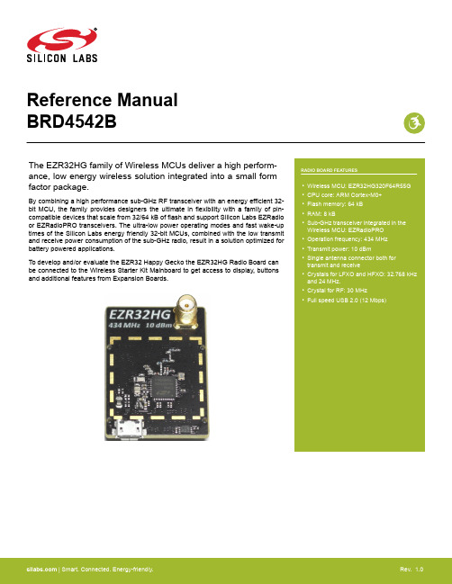
Reference Manual BRD4542BThe EZR32HG family of Wireless MCUs deliver a high perform-ance, low energy wireless solution integrated into a small form factor package.By combining a high performance sub-GHz RF transceiver with an energy efficient 32-bit MCU, the family provides designers the ultimate in flexibility with a family of pin-compatible devices that scale from 32/64 kB of flash and support Silicon Labs EZRadio or EZRadioPRO transceivers. The ultra-low power operating modes and fast wake-up times of the Silicon Labs energy friendly 32-bit MCUs, combined with the low transmit and receive power consumption of the sub-GHz radio, result in a solution optimized for battery powered applications.To develop and/or evaluate the EZR32 Happy Gecko the EZR32HG Radio Board can be connected to the Wireless Starter Kit Mainboard to get access to display, buttonsand additional features from Expansion Boards.Rev. 1.0Introduction 1. IntroductionThe EZR32 Happy Gecko Radio Boards provide a development platform (together with the Wireless Starter Kit Mainboard) for the Silicon Labs EZR32 Happy Gecko Wireless Microcontrollers and serve as reference designs for the matching network of the RF inter-face.The BRD4542B is designed to the operate in the European ETSI 433.05-434.79 MHz band, the RF matching network is optimized to operate in the 434 MHz band with 10 dBm output power.To develop and/or evaluate the EZR32 Happy Gecko the BRD4542B Radio Board can be connected to the Wireless Starter Kit Main-board to get access to display, buttons and additional features from Expansion Boards and also to evaluate the performance of the RF interface.2. Radio Board Connector Pin AssociationsThe figure below shows the pin mapping on the connector to the radio pins and their function on the Wireless Starter Kit Mainboard.GND F9 / NC3v3NC / P36P200Upper RowNC / P38NC / P40NC / P42NC / P44DEBUG.TMS_SWDIO / PF1 / F0DISP_ENABLE / PA1 / F14UIF_BUTTON0 / PC9 / F12UIF_LED0 / PF4 / F10NC / F8DEBUG.RESET / RESETn / F4NC / F2DISP_MOSI / PE10 / F16VCOM.TX_MOSI / PD4 / F6PTI.DATA / RF_GPIO0 / F20DISP_EXTCOMIN / PF3 / F18USB_VBUS5VBoard ID SCLGNDBoard ID SDAUSB_VREGF7 / PD5 / VCOM.RX_MISOF5 / PC8 / VCOM_ENABLEF3 / NCF1 / PF0 / DEBUG.TCK_SWCLKP45 / NCP43 / NCP41 / NCP39 / NCP37 / NCF11 / PF2 / UIF_LED1F13 / PC10 / UIF_BUTTON1F15 / PE12 / DISP_SCLKF17 / PA0 / DISP_SCSF19 / RF_GPIO1 / PTI.SYNCF21 / NCGNDVMCU_INUIF_LED1 / PF2 / P0P201Lower RowUIF_LED0 / PF4 / P2UIF_BUTTON0 / PC9 / P4UIF_BUTTON1 / PC10 / P6GND VRF_INP35 / P7 / PE13P5 / PE12 / DISP_SCLK P3 / PE11P1 / PE10 / DISP_MOSI P33 / RF_GPIO3 P31 / RF_GPIO1 / PTI.SYNC P29 / NCP27 / NC P25 / PC14 * P23 / NC P21 / PF1 / DEBUG.TMS_SWDIO P19 / PC8 / VCOM_ENABLEP17 / NCP15 / PA1 / DISP_ENABLE P13 / PD6P11 / PD5 / VCOM.RX_MISO P9 / PD4 / VOM.TX_MOSI NC / P34RF_GPIO2 / P32PTI.DATA / RF_GPIO0 / P30NC / P28PC15 * / P26NC / P24DISP_EXTCOMIN / PF3 / P22DEBUG.TCK_SWCLK / PF0 / P20NC / P18NC / P16DISP_SCS / PA0 / P14PD7 / P12NC / P10PB11 / P8 * Connection is not enabled by default on the Radio Board.To enable 0 Ohm resistors should be mounted. See the schematic of the Radio Board.Figure 2.1. BRD4542B Radio Board Connector Pin MappingRadio Board Connector Pin Associations3. Radio Board Block DescriptionThe block diagram of the EZR32HG Radio Board is shown in the figure below. For the exact part numbers of the applied components refer to the BRD4542B BOM.Figure 3.1. EZR32HG Radio Board Block Diagram3.1 Wireless MCUThe BRD4542B EZR32 Happy Gecko Radio Board incorporates an EZR32HG320F64R55G Wireless Microcontroller featuring 32-bit Cortex-M0+ core, 64 kB of flash memory and 8 kB of RAM. For additional information on the EZR32HG320F64R55G, refer to the EZR32HG320 Data Sheet.The EZR32HG320F64R55G is built using the Si4455, a high-performance, low-current transciever that is part of Silicon Labs' EZRadio family. The Si4455 contains a +13 dBm power amplifier that is capable of transmitting from –40 to +13 dBm. For a complete feature set and in-depth information on the transciever, refer to the "Si4455 Easy-to-Use, Low-Current OOK/(G)FSK Sub-GHz Transceiver" Data Sheet.3.2 USBThe BRD4542B Radio Board incorporates a micro USB connector. The 3.3V USB regulator output is are routed back to the WSTK through the Radio Board Connector so the Radio Board can supply power to the Wireless Starter Kit Mainboard.For additional information on EZR32HG USB, refer to the EZR32HG320 Data Sheet.3.3 RF Crystal Oscillator (RFXO)The BRD4542B Radio Board has a 30 MHz crystal mounted. For more details on crystal or TCXO selection for the RF part of the EZR32 devices refer to "AN785: Crystal Selection Guide for the Si4x6x RF ICs".3.4 LF Crystal Oscillator (LFXO)The BRD4542B Radio Board has a 32.768 kHz crystal mounted. For safe startup two capacitors are also connected to the LFXTAL_N and LFXTAL_H pins. For details regarding the crystal configuration, the reader is referred to Application Note "AN0016: EFM32 Oscilla-tor Design Consideration".| Smart. Connected. Energy-friendly.Rev. 1.0 | 33.5 HF Crystal Oscillator (HFXO)The BRD4542B Radio Board has a 24 MHz crystal mounted. For safe startup two capacitors are also connected to the HFXTAL_N and HFXTAL_H pins. For details regarding the crystal configuration, the reader is referred to Application Note "AN0016: EFM32 Oscillator Design Consideration".3.6 RF Matching NetworkThe BRD4542B Radio Board includes a Class E type matching network with a so-called Direct Tie matching configuration where the TX and RX sides are connected together without an additional RF switch, to be able to use one antenna both for transmitting and receive-ing. The component values were optimized for the 434 MHz band RF performace and current consumption with 10 dBm output power. For more details on the matching network used on the BRD4542B see Chapter 4.1 Matching Network.3.7 SMA ConnectorTo be able to perform conducted measurements or mount external antenna for radiated measurements, range tests etc., Silicon Labs added an SMA connector to the Radio Board. The connector allows an external 50 Ohm cable or antenna to be connected during de-sign verification or testing.3.8 Radio Board ConnectorsTwo dual-row, 0.05” pitch polarized connectors make up the EZR32HG Radio Board interface to the Wireless Starter Kit Mainboard. For more information on the pin mapping between the EZR32HG320F64R55G and the Radio Board Connector refer to Chapter 2. Radio Board Connector Pin Associations.4. RF SectionThe BRD4542B Radio Board includes a Class E type TX matching network with the targeted output power of 10 dBm at 434 MHz.The main advantage of the Class E matching types is their very high efficiency. They are proposed for applications where the current consumption is most critical, e.g., the typical total EZRadio chip current with Class E type matching is ~18 mA at ~10 dBm (using the 13dBm PA output and assuming 3.3 V supply voltage).The main disadvantage of the Class E type matches is the high supply voltage dependency (the power variation is proportional to the square of the supply voltage change: i.e. the decrease in power can be ~6 dB in the 1.8–3.8 V range) and the inaccurate nonlinear power steps. Also their current consumption and the peak voltage on the TX pin are sensitive to the termination impedance variation, and they usually require slightly higher order filtering and thus higher bill of materials cost.The matching network is constructed with a so-called Direct Tie configuration where the TX and RX sides are connected together with-out an additional RF switch, to be able to use one antenna both for transmitting and receiveing. Careful design procedure was followed to ensure that the RX input circuitry does not load down the TX output path while in TX mode and that the TX output circuitry does not degrade receive performance while in RX mode.For detailed explanation of the Class E type TX matching and the Direct Tie configuration matching procedure the reader is referred to "AN693: Si4455 Low-Power PA Matching". For detailed description of the RX matching the reader is referred to "AN643: Si446x/Si4362 RX LNA Matching".4.1 Matching NetworkThe matching network structure used on the BRD4542B Radio Board is shown in the figure below.Figure 4.1. RF Section of the Schematic of the BRD4542B EZR32 Happy Gecko Radio BoardThe component values were optimized for the 434 MHz band RF performace and current consumption with 10 dBm output power. The resulting component values with part numbers are listed in the table below.Rev. 1.0 | 5Table 4.1. Bill of Materials for the BRD4542B RF Matching NetworkThe Application Note "AN693: Si4455 Low-Power PA Matching" contains component values for reference matching networks which were developed for the EZRadioPRO Pico Boards. For the WSTK radio boards some fine-tuning of the component values may be nec-essary due to different parasitic effects (bonding wire, layout etc.). For optimized RF performance the component values listed in the table above may differ from the ones listed in the referred Application Note.For the reader’s specific application and board layout the adjustment of the final matching values might be necessary. The above com-ponent values should be used as starting points and the values modified slightly to zero-in on the best filter response and impedance match to 50 ohm. To minimize the differences due to different layout parasitics Silicon Labs recommends copying the layout of the RF section of the radio board as is. If that is not possible, refer to "AN685: Layout Design Guide for the Si4455/435x RF ICs" for layout design recommendations. | Smart. Connected. Energy-friendly.Rev. 1.0 | 65. Mechanical DetailsThe BRD4542B EZR32 Happy Gecko Radio Board is illustrated in the figures below.2.7 mmFigure 5.1. BRD4542B Top View5 mm ConnectorConnector Figure 5.2. BRD4542B Bottom ViewMechanical DetailsRev. 1.0 | 7EMC Compliance 6. EMC ComplianceThe BRD4542B EZR32 Happy Gecko Radio Board is dedicated for operation in the European ETSI 434.050-434.790 MHz band for non-specific use. The relevant ETSI EN 300-220-1 regulation specifies the maximum allowed level of the fundamental power and spuri-ous emissions.In this document the compliance of the Radio Board fundamental power and harmonic emissions with the regulation limits will be inves-tigated at 434MHz (up to the frequency of the 10th harmonic).6.1 ETSI EN 300-200-1 Emission Limits for the 433.050-434.790 MHz BandBased on ETSI EN 300-220-1 the allowed maximum fundamental power for the 433.050-434.790 MHz band is 10 mW (+10 dBm) e.r.p. both for conducted and radiated measurements.Note: Further in this document EIRP (Effective Isotropic Radiated Power) will be used instead of e.r.p. (Effective Radiated Power) for the comparison of the limits and measurement results. The 10 mW e.r.p radiated limit is equivalent to +12.1 dBm EIRP.For the unwanted emission limits see the table below.7. RF Performance7.1 Measurement setupThe BRD4542B EZR32 Happy Gecko Radio Board was attached to a Wireless Starter Kit Mainboard (BRD4001 (Rev. A02) ) and its transceiver was operated in continuous carrier transmission mode. The output power of the radio was set to 10 dBm (PA_PWR_LVL =0x1F, PA_BIAS_CLKDUTY = 0xC0 at VRF=3.3 V).7.2 Conducted Power MeasurementsIn case of the conducted measurements the output power was measured by connecting the EZR32HG Radio Board directly to a Spec-trum Analyzer (P/N: MS2692A) through its on-board SMA connector. At 10 dBm output power and 3.3 V supply voltage the measured typical current consumption of the RF section of the board is 18 mA.A typical output spectrum is shown in the figure below.Figure 7.1. Typical Output Spectrum of the BRD4542B Radio BoardRF Performance| Smart. Connected. Energy-friendly.Rev. 1.0 | 9As it can be observed the only unwanted emission above -60 dBm is the double-frequency harmonic but its -39.39 dBm power is com-pliant with the -27.8 dBm limit with large margin.Note: In practice comercially available whip antennas usually have ~0-2 dB gain at the fundamental and < 0 dB gain at the harmonic frequencies so if the conducted levels are compliant with the emission limits with small margin it is likely that the margin on the harmon-ics radiated by an external whip antenna will be higher. Unfortunately in most cases, the PCB radiation (from traces or and/or compo-nents) is stronger so using shielding, applying larger duty cycle correction (if allowed) or reduction of the fundamental power could be necessary.7.3 Radiated Power MeasurementsFor radiated measurements an external whip antenna (P/N: ANT-433-CW-QW-SMA) was used. The power supply for the board were two AA batteries (3 V). The batteries were connected to the Wireless Starter Kit Mainboard through its External Power Supply connec-tor with minimal wire length to minimize the wire radiation.The DUT was rotated in 360 degree with horizontal and vertical reference antenna polarizations in the XY, XZ and YZ cuts. The meas-urement axes are as shown in the figure below.Figure 7.2. DUT: Radio Board with Wireless Starter Kit Mainboard (Illustration)The measured radiated powers are shown in the table below.Table 7.1. Maximums of the Measured Radiated Powers of the BRD4542BAs it can be observed the fundamental and all of the harmonics comply with the ETSI EN 300-220-1 limits with large margin.One may notice that the radiated harmonic levels, in general, are higher compared to the levels expected based on the conducted measurement. Investigations showed that this increase is due to the PCB radiations (components and PCB traces).Note: The radiated measurement results presented in this document were recorded in an unlicensed antenna chamber. Also the radi-ated power levels may change depending on the actual application (PCB size, used antenna etc.) therefore the absolute levels and margins of the final application is recommended to be verified in a licensed EMC testhouse!EMC Compliance Recommendations 8. EMC Compliance Recommendations8.1 Recommendations for ETSI ComplianceAs it was shown in the previous chapters the BRD4542B EZR32 Happy Gecko Radio Board is compliant with the harmonic emission limits of the ETSI EN 300-220-1 regulation in the 434.050-434.790 MHz band with 10 dBm output power. Although the BRD4542B Radio Board has an option for mounting a shielding can, that is not required for the compliance. Due to the conducted fundamental is marginally exceeding the limit slight output power reduction could be necessary for the radiated compliance.Document Revision History 9. Document Revision HistoryTable 9.1. Document Revision HistoryBoard Revisions 10. Board RevisionsTable 10.1. BRD4542B Radio Board RevisionsTable of Contents1. Introduction (1)2. Radio Board Connector Pin Associations (2)3. Radio Board Block Description (3)3.1 Wireless MCU (3)3.2 USB (3)3.3 RF Crystal Oscillator (RFXO) (3)3.4 LF Crystal Oscillator (LFXO) (3)3.5 HF Crystal Oscillator (HFXO) (4)3.6 RF Matching Network (4)3.7 SMA Connector (4)3.8 Radio Board Connectors (4)4. RF Section (5)4.1 Matching Network (5)5. Mechanical Details (7)6. EMC Compliance (8)6.1 ETSI EN 300-200-1 Emission Limits for the 433.050-434.790 MHz Band (8)7. RF Performance (9)7.1 Measurement setup (9)7.2 Conducted Power Measurements (9)7.3 Radiated Power Measurements (11)8. EMC Compliance Recommendations (13)8.1 Recommendations for ETSI Compliance (13)9. Document Revision History (14)10. Board Revisions (15)Table of Contents (16)DisclaimerSilicon Laboratories intends to provide customers with the latest, accurate, and in-depth documentation of all peripherals and modules available for system and software implementers using or intending to use the Silicon Laboratories products. Characterization data, available modules and peripherals, memory sizes and memory addresses refer to each specific device, and "Typical" parameters provided can and do vary in different applications. Application examples described herein are for illustrative purposes only. Silicon Laboratories reserves the right to make changes without further notice and limitation to product information, specifications, and descriptions herein, and does not give warranties as to the accuracy or completeness of the included information. Silicon Laboratories shall have no liability for the consequences of use of the information supplied herein. This document does not imply or express copyright licenses granted hereunder to design or fabricate any integrated circuits. The products must not be used within any Life Support System without the specific written consent of Silicon Laboratories. A "Life Support System" is any product or system intended to support or sustain life and/or health, which, if it fails, can be reasonably expected to result in significant personal injury or death. Silicon Laboratories products are generally not intended for military applications. Silicon Laboratories products shall under no circumstances be used in weapons of mass destruction including (but not limited to) nuclear, biological or chemical weapons, or missiles capable of delivering such weapons.Trademark InformationSilicon Laboratories Inc., Silicon Laboratories, Silicon Labs, SiLabs and the Silicon Labs logo, CMEMS®, EFM, EFM32, EFR, Energy Micro, Energy Micro logo and combinations thereof, "the world’s most energy friendly microcontrollers", Ember®, EZLink®, EZMac®, EZRadio®, EZRadioPRO®, DSPLL®, ISOmodem ®, Precision32®, ProSLIC®, SiPHY®, USBXpress® and others are trademarks or registered trademarks of Silicon Laboratories Inc. ARM, CORTEX, Cortex-M3 and THUMB are trademarks or registered trademarks of ARM Holdings. Keil is a registered trademark of ARM Limited. All other products or brand names mentioned herein are trademarks of their respective holders.Silicon Laboratories Inc.400 West Cesar Chavez Austin, TX 78701USASimp li city StudioOne-click access to MCU tools, documentation, software, source code libraries & more. Available for Windows, Mac and Linux!/simplicityMCU Portfolio /mcuSW/HW/simplicityQuality /qualitySupport and Community。
Silicon Labs 自动化系统隔离产品说明书

How to Solve EMI Problems in Isolated Automotive SystemsBy Charlie Ice, Senior Product Manager, Isolation, Silicon LabsIntroductionElectromagnetic compatibility (EMC) has long been a challenge for engineers, and as electric vehicle (EV) and hybrid electric vehicle (HEV) systems continue to gain momentum, this continues to be a major concern. Traditional internal combustion engine (ICE) vehicles are largely mechanicalin nature, with electronics bolted to the mechanical power plant. EVs and HEVs, however, are very different. Electrical power is converted into mechanical motion using high-voltage batteries, motors, and chargers. With great power comes great responsibility... to limit the electromagnetic interference (EMI) that comes with power electronics! The isolation used to bridge the low voltage and high voltage domains also introducesnew EMI concerns. Many modern EVs and HEVs use digital isolators, which bring unprecedented levels of sophistication and capability to isolation devices and are designed to minimize EMI. However, they are still a digital device that can cause EMI issues. Fortunately, there are several tried and true techniques for reducing EMI in an isolated system, and three of the most effective don’t add any additional cost.Before tackling EMI improvements, or the EMI standards for vehicles, the basics of electromagnetic compatibility (EMC) and EMI must be understood. EMC refers to both the immunity and emissions of a device, while EMI focuses only on the emissions of a device. CISPR 25, the most common EMC standard used for vehicles, specifies both EMI and immunity requirements. A device’s ability to operate correctly despite the presence of interference is known as immunity. Designers generally place and emphasis on reducing the EMI of a device because it tends to improve its immunity to outside interference.EMI is divided into conducted and radiated emission limits within CISPR 25, and the difference between the two is fairlyintuitive. Conducted EMI travels between devices through the power, signaling, or other connected cables. This is in contrast to radiated EMI, which travels through electromagnetic fields in order to interfere other devices. Radiated EMI, on the other hand, travels through electromagnetic fields to interfere with the other device. Radios illustrate this concept well because the radio transmitter is emitting specific frequencies of radiated EMI that the receiver is tuned to pick up. The same holds true for unwanted radiated EMI - the offending device transmits an unwanted electromagnetic field, which the other device unintentionally receives and amplifies. Unlike a radio, this received signal results in the device operating unintentionally. EMC standards for EMI ensure the conducted and radiated emissions are below a specified threshold under specific test conditions. By passing the EMI tests outlined in CISPR 25, a device is unlikely to interfere with another device in the vehicle.Differential-mode and common-mode currents are an important part of any discussion about EMI. As common-mode currents often cause EMI, the vast majority of circuits operate by using differential-mode current. Figure 1 shows a single-endedsignaling scheme using differential-mode current, where current is sent on one conductor and then returned through the ground connection. Another differential-mode signaling method is to use balanced differential signaling, where a dedicated conductor is added for the return current, as shown in Figure 2. In both methods, the current in the two conductors is the same leaving a net zero current. Unfortunately, many times the return current finds an alternative, often longer, path back to the source resulting in a common-mode current. This common-mode current creates an imbalance in the two conductors which causes radiated emissions. Figures 3 and 4 show common-mode currents for both single ended and differential-mode systems. Fortunately, many common-mode currents can be reduced with a few design improvements. Before exploring these methods, however, the additional challenges brought about by isolation must be discussed.Immunity, Emissions, and CurrentsFigure 1 - Single-ended differential-mode current.Load (RX)VS VLi sourceV diffi returnSource (TX)Figure 2 - Balanced differential-mode current.Load (RX)VS VLi sourceV diffi returnSource (TX)Figure 3 - Common-mode current in a single ended system.VS VLFigure 4 - Common-mode current in a differential signaling system.VS VLcmIsolation, and digital isolation in particular, is one of the fundamental technologies enabling the electric vehicle revolution. The isolation device allows communication and signaling across the high impedance barrier between the high voltage and low voltage domains. Figure 5 shows a basic isolation diagram. Among many other use cases and benefits, the isolation barrier allows the low voltage electronics, often the controller, to be separated from the high voltage portion of the system. Digital isolation leverages CMOS technology to replace traditional optocouplers and bring greater sophistication and integration than ever before to the isolation device. Silicon Labs’ digital isolators use capacitors and high frequency signaling to create the isolation barrier and pass information across it. To minimize emissions, the internal capacitors are very well matched, and signals are sent using balanced differential signaling. This requires two capacitors to create a single digital channel, as shown in Figure 6. Even with these techniques, isolation in a system, and digital isolation technology itself, introduces new EMI challenges.EMI Challenges from IsolationFigure 5 - Isolation creates a very high impedance between two grounds in a system, effectively eliminating the electrical connection between them.Supply Voltage A Ground A Ground BVery High Impedance Between Grounds A and B Supply Voltage BDC DCCircuit B Signals Figure 6 - Silicon Labs digital isolation channel and balanced differential signaling.Input voltage threshold comparator and OOK Modulator +AC VDDAPower Domain A Power Domain BI s o l a t i o n B a r r i e r Differential RF Carrier Transmitter Matched Iso-CapacitorsSilicon Labs Isolator Channel Ax InputGNDA-AC VDDB Bx Output GNDBDetector and push-pull digital outputThe separation of the power domains creates a high impedance path between the two circuits, as shown in Figure 5. This high impedance path creates a problem for common mode currents induced by large changes in voltage (dv/dt) present on one side and not the other. These E-field induced currents have to find a path back to their source and their paths are often long, not well defined, and high impedance. Eventually, the current returns through parasitic capacitance between the power domains. The large loop area created by these currents can lead to increased conducted and radiated emissions. Minimizing these common mode currents usually involves placing a capacitor across the isolation barrier (known as a Y capacitor) or even interleaving the PCB planes to add additional capacitance. This extra capacitance provides a low impedance, short path for the high frequency current to return to its source. Detailed analysis of Y capacitor placement and PCB inner plane capacitor design can be foundin Silicon Lab’s application note– AN1131: Design Guide for Reducing EMI in Isolated Systems. However, before diving into the intricacies of E-fields and capacitance calculations, many EMI problems can be solved using traditional EMI best practices with a few modifications specific to digital isolators. Three of the most common, and successful, come at no additional cost and involve component selection and careful layout.Digital isolators leverage CMOS technology to create the isolation barrier and transmit signals across them. Silicon Labs’ digital isolators use silicon dioxide to build high voltage capacitors that maintain the isolation barrier. Signals are transmitted across the capacitive barrier using high frequency RF signals. By leveraging on/off keying (OOK) modulation, the RF transmitter is only active during one of the two logic states, as shown in Figure 7. The default output configuration determines when an RF transmitter will be active. If the signal being sent by the isolator is typically either high or low, simply choosing the matching default output state will minimize the transmissions, reducing EMI and power consumption. For example, when isolating a SPI bus with the idle state high, selecting an isolator with an output default high decreases the RF transmissions of the isolator. Figure 8 illustrates the difference between a default low and default high isolator for this SPI bus configuration. In the Silicon Labs’ Si86xx family of digital isolators, Si86xxBx part numbers use low as their default state, while Si86xxEx default to output high. With the proper digital isolator selected, the components around the isolation device may now be optimized for EMI.Method 1: Select the Isolator that Minimizes TransmissionsFigure 7 - Silicon Labs OOK modulation.Figure 8 - Reducing RF transmissions by selecting the default output state of the isolator.Ax Input SignalBx Output SignalOn/Off Keyed RF TransmitterBus Activity CSSCLKSDA‘E’ Ordering Option Modulated Carrier Transmission ‘B’ Ordering Option Modulated Carrier Transmission CSSCLK SDACSSCLK SDAVirtually every digital isolator specifies using a bypass capacitor on the supply pins, and they have a tremendous impact on the EMI performance of the system. The bypass capacitors help reduce AC noise on the power rails. Many times, AC noise results from ripple on the power supply rail due to transient loads from the digital isolator’s normal operation. The bypass capacitors supply additional current to the device during these transient loads, effectively reducing the ripple on the power supply rail. In addition, the bypass capacitors short AC noise to ground and prevent it from entering the digital isolator. Careful selection and placement of the bypass capacitors maximizes their effectiveness.Capacitors act as a short to AC current and a high impedance to DC current. In other words, as the frequency increases the impedance of an ideal capacitor decreases. This holds true in the real world to point. Actual capacitors have an effective series resistance (ESR) and effective series inductance (ESL) due to their construction. As the frequency increases, the ESL eventually dominates, and the capacitor’s impedance begins to increase at the self-resonant frequency. Therefore, reducing the capacitor’s ESL raises the self-resonant frequency and hence, the frequency at which the capacitor’s impedance starts to increase. Figure 9 illustrates this graphically. In general, a smaller sized capacitor will have a lower ESL because ESL depends on the distance between the two capacitor ends. For example, simply moving from an 0805 package size to an 0402 sized capacitor will improve the bypass capacitor’s effectiveness. Furthermore, there are even capacitors built with “reverse geometry” to provide an even lower ESL, as shown in Figure 10. Nonetheless, even with the lowest ESL possible, the placement of the bypass capacitor also plays a critical role.Method 2: Select the Right Bypass CapacitorsNon-ideal Capacitor Model C I m p e d a n c e (l o g s c a l e )Frequency (log scale)Self-resonant frequencyLower ESL will increase the self-resonant frequency for same capacitance value ESR ESL Impedance vs. Frequency of a Non-ideal CapacitorX C =1/wC X L =w E S L Figure 9 - Real world capacitor model and impedance vs frequency.Figure 10 - Standard vs reverse geometry capacitors.Standard 0402 capacitor Reverse geometry 0204 capacitorProperly placing bypass capacitors is just as important as selecting ones with low ESL because traces and vias on the PCBintroduce series inductance. The series inductance of a trace increases with length, making short and wide traces ideal. Also, the length of the return path to the ground pin of digital isolator adds additional series inductance. Simply rotating the capacitor to be close to both the supply and ground pins often reduces the return path length. Figure 11 illustrates ideal placement and non-ideal placement of bypass capacitors. Using these techniques to select low ESL capacitors and optimize the PCB design will maximize the EMI reduction from the bypass capacitors.The EMI principles and techniques shared here provide a foundational understanding of what to consider for designing anautomotive system to meet strict CISPR 25 requirements. For more best practices and explanations of the theories behind EMI, check out Silicon Lab’s application note entitled AN1131: Design Guide for Reducing EMI in Isolated Systems . As vehicle systems become more sophisticated and as electric vehicles become more advanced, EMI will continue to be an important consideration. Isolation is only becoming more important as electric vehicle systems adopt higher voltages to drive greater efficiency. Byconsidering EMI and applying best practices upfront, high-voltage, isolated automotive systems will be ready to pass today and tomorrow’s EMI requirements.Method 3: Optimize Bypass Capacitor PlacementFigure 11 - Optimizing the placement of bypass capacitors.Charlie Ice is a Senior Product Manager at Silicon Labs focusing on the company’s Power overEthernet (PoE) and automotive product lines. Charlie joined Silicon Labs in 2018 with more than 10years managing products in the technology industry. His experience includes microcontrollers, digitalmotor control, digital power supply control, and test and measurement equipment. Prior to joiningSilicon Labs, Charlie managed the hardware resell program at National Instruments after marketingdigital motor control MCUs at Texas Instruments and Microchip Technology. Charlie holds a Masterand Bachelor of Science in Electrical Engineering, both from Rice University in Houston, Texas.。
芯科科技推出全新系列隔离模拟放大器、电压传感器和Delta-Sigma调制器(DSM)器件

编者按:今日,芯科科技推出了一系列新产品,产品使用第三代技术具有更高标准,新产品更浪涌性能、可靠性、集成度和安全性。
日前,芯科科技(Silicon Labs,NASDAQ:SLAB)推出了一系列隔离模拟放大器、电压传感器和Delta-Sigma调制器(DSM)器件,设计旨在整个温度范围内提供超低温漂的精确电流和电压测量。
新型Si89xx系列产品基于Silicon Labs强大的第三代隔离技术,可提供灵活的电压、电流测量,并且有丰富的输出接口和封装选项,帮助开发人员降低BOM成本、减小电路板空间,适用于各种工业和绿色能源应用,包括电动汽车(EV)电池管理和充电系统、DC-DC 转换器、电动机、太阳能和风力涡轮机逆变器等。
精确电流和电压测量对于功率控制系统的精确操作至关重要。
为了最大限度地提高效率并对故障或负载变化快速响应,系统控制器需要来自高压供电线上的电流和电压信息。
Silicon Labs的第三代隔离技术可在1414V工作电压和13kV双极性浪涌的情况下保持控制器在较宽温度范围内的安全性,并超越严格的行业要求。
据介绍,Silicon Labs现在可提供业界最广泛的电流和电压传感器产品组合。
Si89xx系列包括四个产品类别:•Si892x隔离模拟放大器,特别针对电流分流检测进行了优化。
•Si8931/2隔离模拟放大器,特别针对通用电压检测进行了优化。
•Si8935/6/7隔离DSM器件,业界首创特别针对电压检测进行了优化。
•Si8941/6/7隔离DSM器件,特别针对电流分流检测进行了优化。
Silicon Labs副总裁兼电源产品总经理Brian Mirkin表示:“在过去的十年间,我们的第一代和第二代混合信号隔离技术推动我们数字隔离产品在市场上取得巨大的成功,我们在新型Si89xx器件中使用的第三代技术具有更高标准。
我们的隔离产品将继续取代传统的光耦合器,并且优于竞争对手的数字隔离器,这为需要高压保护的系统设计提供了更高的浪涌性能、可靠性、集成度和一流的安全性。
Silicon Labs Si534xH 相干光时钟产品介绍说明书

新闻稿Silicon Labs降低相干光市场定时技术的成本和复杂度-单芯片Si534xH时钟系列产品为100G/400G收发器提供高性能、频率灵活的定时解决方案-中国,北京-2016年4月26日-Silicon Labs(芯科科技有限公司,NASDAQ:SLAB)日前推出一系列简化100G/400G相干光线卡(coherent optical line card)和模块设计的抖动衰减时钟,通过提供高频率、灵活的时钟解决方案,显著降低系统成本和复杂度。
Silicon Labs新型Si534xH相干光时钟可以为数据转换器提供低抖动参考定时,可替代依赖于昂贵、大封装尺寸的压控SAW振荡器(VCSO)的分立定时解决方案。
与仅支持单一固定频率的VCSO不同,新型Si534xH时钟提供很宽的频率范围,支持频率高达2.7GHz,且无需改变物料清单(BOM)元器件。
Si5344H和Si5342H时钟提供最佳的频率灵活性和无与伦比的50fs RMS抖动性能。
这些时钟芯片简化了器件采购过程,可采用较短的、两周交货时间的单个时钟IC解决方案替代多个定制的、较长交货时间的VCSO。
凭借抖动衰减PLL、高频率输出驱动器、分数频率合成和数字控制振荡器(DCO)技术,Si534xH系列产品为相干光收发器应用提供所需的全部时钟功能,与竞争对手解决方案相比降低了40%的占用面积及40%的功耗。
获取Silicon Labs Si534xH相干光时钟的更多详细信息,包括数据手册、支持文档和开发工具等,请访问网站:/timing。
通信市场中最大增长驱动因素之一是业内城域网络和数据中心互联(DCI)领域从10G 到100G的转变。
相干光学技术可用于100G和400G应用,因为它使得服务提供商能够通过现有的光纤发送更多的数据,减少为带宽扩展而进行网络升级的成本和复杂性。
当前用于相干光的定时解决方案在成本和尺寸方面还未达到最优化,需要VCSO、时钟发生器和分立器件的多样化组合。
Silicon Labs EFR32MG 2.4 GHz 19.5 dBm 无线模组板参考手册说明书
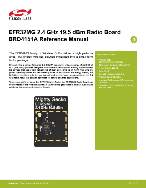
EFR32MG 2.4 GHz 19.5 dBm Radio BoardBRD4151A Reference Manualance, low energy wireless solution integrated into a small formfactor package.By combining a high performance 2.4 GHz RF transceiver with an energy efficient 32-bitMCU, the family provides designers the ultimate in flexibility with a family of pin-compati-ble devices that scale from 128/256 kB of flash and 16/32 kB of RAM. The ultra-lowpower operating modes and fast wake-up times of the Silicon Labs energy friendly 32-bit MCUs, combined with the low transmit and receive power consumption of the 2.4GHz radio, result in a solution optimized for battery powered applications.To develop and/or evaluate the EFR32 Mighty Gecko, the EFR32MG Radio Board canbe connected to the Wireless Starter Kit Mainboard to get access to display, buttons andadditional features from Expansion Boards.Introduction 1. IntroductionThe EFR32 Mighty Gecko Radio Boards provide a development platform (together with the Wireless Starter Kit Mainboard) for the Silicon Labs EFR32 Mighty Gecko Wireless System on Chips and serve as reference designs for the matching network of the RF inter-face.The BRD4151A Radio Board is designed to operate in the 2400-2483.5 MHz band with the RF matching network optimized to operate with 19.5 dBm output power.To develop and/or evaluate the EFR32 Mighty Gecko, the BRD4151A Radio Board can be connected to the Wireless Starter Kit Main-board to get access to display, buttons and additional features from Expansion Boards and also to evaluate the performance of the RF interface.2. Radio Board Connector2.1 IntroductionThe board-to-board connector scheme allows access to all EFR32MG1 GPIO pins as well as the RESETn signal. For more information on the functions of the available pin functions, see the EFR32MG1 data sheet.2.2 Radio Board Connector Pin AssociationsThe figure below shows the pin mapping on the connector to the radio pins and their function on the Wireless Starter Kit Mainboard.GND F9 / PA3 / VCOM.#RTS_#CS 3v3UIF_BUTTON1 / PF7 / P36P200Upper RowNC / P38NC / P40NC / P42NC / P44DEBUG.TMS_SWDIO / PF1 / F0DISP_ENABLE / PD15 / F14UIF_BUTTON0 / PF6 / F12DISP_EXTCOMIN / PD13 / F10VCOM.#CTS_SCLK / PA2 / F8#RESET / F4DEBUG.TDO_SWO / PF2 / F2DISP_SI / PC6 / F16VCOM.TX_MOSI / PA0 / F6PTI.DATA / PB12 / F20DISP_EXTCOMIN / PD13 / F18USB_VBUS5VBoard ID SCLGND Board ID SDAUSB_VREG F7 / PA1 / VCOM.RX_MISO F5 / PA5 / VCOM_ENABLE F3 / PF3 / DEBUG.TDI F1 / PF0 / DEBUG.TCK_SWCLK P45 / NC P43 / NCP41 / NCP39 / NCP37 / High / SENSOR_ENABLEF11 / PF5 / UIF_LED1F13 / PF7 / UIF_BUTTON1F15 / PC8 / DISP_SCLK F17 / PD14 / DISP_SCS F19 / PB13 / PTI.SYNC F21 / PB11 / PTI.CLK GNDVMCU_INVCOM.#CTS_SCLK / PA2 / P0P201Lower RowVCOM.#RTS_#CS / PA3 / P2PD10 / P4PD11 / P6GND VRF_INP35 / PD15 / DISP_ENABLE P7 / PC9P5 / PC8 / DISP_SCLK P3 / PC7P1 / PC6 / DISP_SI P33 / PD14 / DISP_SCSP31 / PD13 / DISP_EXTCOMIN P29 / NCP27 / NC P25 / NC P23 / NC P21 / NC P19 / NC P17 / NC P15 / NC P13 / PC11P11 / PA1 / VCOM.RX_MISO P9 / PA0 / VCOM.TX_MOSI UIF_BUTTON0 / PF6 / P34UIF_LED1 / PF5 / P32UIF_LED0 / PF4 / P30DEBUG.TDO_SWO / PF2 / P28DEBUG.TMS_SWDIO / PF1 / P26DEBUG.TCK_SWCLK / PF0 / P24PTI.SYNC / PB13 / P22PTI.DATA / PB12 / P20PTI.CLK / PB11 / P18VCOM_ENABLE / PA5 / P16PA4 / P14PC10 / P12DEBUG.TDI / PF3 / P10PD12 / P8Figure 2.1. BRD4151A Radio Board Connector Pin MappingRadio Board Connector3. Radio Board Block Summary3.1 IntroductionThis section gives a short introduction to the blocks of the BRD4151A Radio Board.3.2 Radio Board Block DiagramThe block diagram of the EFR32MG Radio Board is shown in the figure below.Figure 3.1. BRD4151A Block Diagram3.3 Radio Board Block Description3.3.1 Wireless MCUThe BRD4151A EFR32 Mighty Gecko Radio Board incorporates an EFR32MG1P232F256GM48 Wireless System on Chip featuring 32-bit Cortex-M4 with FPU core, 256 kB of flash memory and 32 kB of RAM and a 2.4 GHz band transceiver with output power up to 19.5 dBm. For additional information on the EFR32MG1P232F256GM48, refer to the EFR32MG1 Data Sheet.3.3.2 LF Crystal Oscillator (LFXO)The BRD4151A Radio Board has a 32.768 kHz crystal mounted.3.3.3 HF Crystal Oscillator (HFXO)The BRD4151A Radio Board has a 38.4 MHz crystal mounted.3.3.4 Matching Network for 2.4 GHzThe BRD4151A Radio Board incorporates a 2.4 GHz matching network which connects the 2.4 GHz TRX pin of the EFR32MG1 to the one on-board printed Inverted-F antenna. The component values were optimized for the 2.4 GHz band RF performace and current con-sumption with 19.5 dBm output power.For detailed description of the matching network, see Chapter 4.2.1 Description of the 2.4 GHz RF Matching.| Smart. Connected. Energy-friendly.Rev. 1.7 | 33.3.5 Inverted-F AntennaThe BRD4151A Radio Board includes a printed Inverted-F antenna (IFA) tuned to have close to 50 Ohm impedance at the 2.4 GHz band.For detailed description of the antenna see Chapter 4.5 Inverted-F Antenna.3.3.6 UFL ConnectorTo be able to perform conducted measurements, Silicon Labs added an UFL connector to the Radio Board. The connector allows an external 50 Ohm cable or antenna to be connected during design verification or testing.Note: By default the output of the matching network is connected to the printed Inverted-F antenna by a series component. It can be connected to the UFL connector as well through a series 0 Ohm resistor which is not mounted by default. For conducted measurements through the UFL connector the series component to the antenna should be removed and the 0 Ohm resistor should be mounted (see Chapter 4.2 Schematic of the RF Matching Network for further details).3.3.7 Radio Board ConnectorsTwo dual-row, 0.05” pitch polarized connectors make up the EFR32MG Radio Board interface to the Wireless Starter Kit Mainboard. For more information on the pin mapping between the EFR32MG1P232F256GM48 and the Radio Board Connector, refer to Chapter 2.2 Radio Board Connector Pin Associations.4. RF Section4.1 IntroductionThis section gives a short introduction to the RF section of the BRD4151A.4.2 Schematic of the RF Matching NetworkThe schematic of the RF section of the BRD4151A Radio Board is shown in the following figure.U1BPath Inverted-F Antenna2.4 GHz Matching Figure 4.1. Schematic of the RF Section of the BRD4151A4.2.1 Description of the 2.4 GHz RF MatchingThe 2.4 GHz matching connects the 2G4RF_IOP pin to the on-board printed Inverted-F Antenna. The 2G4RF_ION pin is connected to ground. For higher output powers (13 dBm and above) beside the impedance matching circuitry it is recommended to use additional harmonic filtering as well at the RF output. The targeted output power of the BRD4151A board is 19.5 dBm. As a result, the RF output of the IC is connected to the antenna through a four-element impedance matching and harmonic filter circuitry.For conducted measurements the output of the matching network can also be connected to the UFL connector by relocating the series R1 resistor (0 Ohm) to the R2 resistor position between the output of the matching and the UFL connector.4.3 RF Section Power SupplyOn the BRD4151A Radio Board the supply pin of the RF Analog Power (RFVDD) is connected directly ot the output of the on-chip DC-DC converter while the supply for the 2.4 GHz PA (PAVDD) is provided directly by the mainboard. This way, by default, the DC-DC converter provides 1.8 V for the RF analog section, the mainboard provides 3.3 V for the PA (for details, see the schematic of the BRD4151A).4.4 Bill of Materials for the 2.4 GHz MatchingThe Bill of Materials of the 2.4 GHz matching network of the BRD4151A Radio Board is shown in the following table.Table 4.1. Bill of Materials for the BRD4151A 2.4 GHz 19.5 dBm RF Matching Network | Smart. Connected. Energy-friendly.Rev. 1.7 | 54.5 Inverted-F AntennaThe BRD4151A Radio Board includes an on-board printed Inverted-F Antenna tuned for the 2.4 GHz band. Due to the design restric-tions of the Radio Board the input of the antenna and the output of the matching network can't be placed directly next to each other. Therefore, a 50 Ohm transmission line was necessary to connect them. The resulting impedance and reflection measured at the output of the matcing network are shown in the following figure. As it can be observed the impedance is close to 50 Ohm (the reflection is better than -10 dB) for the entire 2.4 GHz band.Figure 4.2. Impedance and Reflection of the Inverted-F Antenna of the BRD4151A| Smart. Connected. Energy-friendly.Rev. 1.7 | 65. Mechanical DetailsThe BRD4151A EFR32 Mighty Gecko Radio Board is illustrated in the figures below.45 mmFigure 5.1. BRD4151A Top View5 mm ConnectorConnectorFigure 5.2. BRD4151A Bottom ViewMechanical DetailsRev. 1.7 | 7EMC Compliance 6. EMC Compliance6.1 IntroductionCompliance of the fundamental and harmonic levels is tested against the following standards:• 2.4 GHz:•ETSI EN 300-328•FCC 15.2476.2 EMC Regulations for 2.4 GHz6.2.1 ETSI EN 300-328 Emission Limits for the 2400-2483.5 MHz BandBased on ETSI EN 300-328 the allowed maximum fundamental power for the 2400-2483.5 MHz band is 20 dBm EIRP. For the unwan-ted emissions in the 1 GHz to 12.75 GHz domain the specified limit is -30 dBm EIRP.6.2.2 FCC15.247 Emission Limits for the 2400-2483.5 MHz BandFCC 15.247 allows conducted output power up to 1 Watt (30 dBm) in the 2400-2483.5 MHz band. For spurious emmissions the limit is -20 dBc based on either conducted or radiated measurement, if the emission is not in a restricted band. The restricted bands are speci-fied in FCC 15.205. In these bands the spurious emission levels must meet the levels set out in FCC 15.209. In the range from 960 MHz to the frequency of the 5th harmonic it is defined as 0.5 mV/m at 3 m distance (equals to -41.2 dBm in EIRP).Additionally, for spurious frequencies above 1 GHz, FCC 15.35 allows duty-cycle relaxation to the regulatory limits. For the EmberZNet PRO the relaxation is 3.6 dB. Therefore, the -41.2 dBm limit can be modified to -37.6 dBm.If operating in the 2400-2483.5 MHz band the 2nd, 3rd and 5th harmonics can fall into restricted bands. As a result, for those the -37.6 dBm limit should be applied. For the 4th harmonic the -20 dBc limit should be applied.6.2.3 Applied Emission Limits for the 2.4 GHz BandThe above ETSI limits are applied both for conducted and radiated measurements.The FCC restricted band limits are radiated limits only. Besides that, Silicon Labs applies those to the conducted spectrum i.e., it is assumed that, in case of a custom board, an antenna is used which has 0 dB gain at the fundamental and the harmonic frequencies. In that theoretical case, based on the conducted measurement, the compliance with the radiated limits can be estimated.The overall applied limits are shown in the table below.Table 6.1. Applied Limits for Spurious Emissions for the 2.4 GHz Band | Smart. Connected. Energy-friendly.Rev. 1.7 | 87. RF Performance7.1 Conducted Power MeasurementsDuring measurements, the EFR32MG Radio Board was attached to a Wireless Starter Kit Mainboard which was supplied by USB. The voltage supply for the Radio Board was 3.3 V.7.1.1 Conducted Measurements in the 2.4 GHz bandThe BRD4151A board was connected directly to a Spectrum Analyzer through its UFL connector (the R1 resistor (0 Ohm) was removed and a 0 Ohm resistor was soldered to the R2 resistor position). During measurements, the voltage supply for the board was 3.3 V provi-ded by the mainboard. The supply for the radio (RFVDD) was 1.8 V provided by the on-chip DC-DC converter, the supply for the power amplifier (PAVDD) was 3.3 V (for details, see the schematic of the BRD4151A). The transceiver was operated in continuous carrier transmission mode. The output power of the radio was set to the maximum level.The typical output spectrum is shown in the following figure.Figure 7.1. Typical Output Spectrum of the BRD4151AAs it can be observed, the fundamental is slightly lower than 19.5 dBm and the strongest unwanted emission is the double-frequency harmonic and it is under the -37.6 dBm applied limit.Note: The conducted measurement is performed by connecting the on-board UFL connector to a Spectrum Analyzer through an SMA Conversion Adapter (P/N: HRMJ-U.FLP(40)). This connection itself introduces approximately a 0.3 dB insertion loss.RF PerformanceRev. 1.7 | 97.2 Radiated Power MeasurementsDuring measurements, the EFR32MG Radio Board was attached to a Wireless Starter Kit Mainboard which was supplied by USB. The voltage supply for the Radio Board was 3.3 V. The radiated power was measured in an antenna chamber by rotating the DUT 360degrees with horizontal and vertical reference antenna polarizations in the XY , XZ and YZ cuts. The measurement axes are shown inthe figure below.Figure 7.2. DUT: Radio Board with the Wireless Starter Kit Mainboard (Illustration)Note: The radiated measurement results presented in this document were recorded in an unlicensed antenna chamber. Also the radi-ated power levels may change depending on the actual application (PCB size, used antenna, and so on). Therefore, the absolute levels and margins of the final application are recommended to be verified in a licensed EMC testhouse.7.2.1 Radiated Measurements in the 2.4 GHz bandFor the transmitter antenna, the on-board printed Inverted-F antenna of the BRD4151A board was used (the R1 resistor (0 Ohm) was mounted). During the measurements the board was attached to a Wireless Starter Kit Mainboard (BRD4001 (Rev. A02) ) which was supplied through USB. During measurements, the voltage supply for the board was 3.3 V provided by the mainboard. The supply for the radio (RFVDD) was 1.8 V provided by the on-chip DC-DC converter, the supply for the power amplifier (PAVDD) was 3.3 V (for details, see the schematic of the BRD4151A). The transceiver was operated in continuous carrier transmission mode. The output power of the radio was set to the maximum level.The results are shown in the table below.Table 7.1. Maximums of the Measured Radiated Powers of BRD4151AAs it can be observed, thanks to the high gain of the Inverted-F antenna, the level of the fundamental is higher than 19.5 dBm. The strongest harmonic is the double-frequency one but its level is under -45 dBm.RF PerformanceEMC Compliance Recommendations 8. EMC Compliance Recommendations8.1 Recommendations for 2.4 GHz ETSI EN 300-328 complianceAs it was shown in the previous chapter, the radiated power of the fundamental of the BRD4151A EFR32 Mighty Gecko Radio Board complies with the 20 dBm limit of the ETSI EN 300-328 in case of the conducted measurement but due to the high antenna gain the radiated power is higher than the limit by 2 dB. In order to comply, the output power should be reduced (with different antennas, de-pending on the gain of the used antenna, the necessary reduction can be different). The harmonic emissions are under the -30 dBm limit. Although the BRD4151A Radio Board has an option for mounting a shielding can, that is not required for the compliance.8.2 Recommendations for 2.4 GHz FCC 15.247 complianceAs it was shown in the previous chapter, the radiated power of the fundamental of the BRD4151A EFR32 Mighty Gecko Radio Board complies with the 30 dBm limit of the FCC 15.247. The harmonic emissions are under the -37.6 dBm applied limit both in case of the conducted and the radiated measurements. Although the BRD4151A Radio Board has an option for mounting a shielding can, that is not required for the compliance.Board Revisions 9. Board RevisionsTable 9.1. BRD4151A Radio Board RevisionsNote: The silkscreen marking on the board (e.g., PCBxxxx A00) denotes the revision of the PCB. The revision of the actual Radio Board can be read from the on-board EEPROM.Errata 10. ErrataTable 10.1. BRD4151A Radio Board ErrataDocument Revision History 11. Document Revision HistoryRevision 1.72016-11-20Minor editorial updates.Revision 1.62016-10-31Corrected error in radio board connector pinout diagram.Revision 1.52016-05-24Updating Board Revisions content. Fixing Errata description.Revision 1.42016-05-05Adding Introduction chapter; moving SoC Description chapter (short ver.) to Block Description chapter. Minor improvements.Revision 1.32016-02-11Addign RF Section Power Supply chapter. Minor improvements.Revision 1.22016-01-28Fixing image render problem.Revision 1.12015-25-25Updating Inverted-F Antenna Chapter and radiated measurement results based on board revision B02.Revision 1.02015-11-27Initial release.Table of Contents1. Introduction (1)2. Radio Board Connector (2)2.1 Introduction (2)2.2 Radio Board Connector Pin Associations (2)3. Radio Board Block Summary (3)3.1 Introduction (3)3.2 Radio Board Block Diagram (3)3.3 Radio Board Block Description (3)3.3.1 Wireless MCU (3)3.3.2 LF Crystal Oscillator (LFXO) (3)3.3.3 HF Crystal Oscillator (HFXO) (3)3.3.4 Matching Network for 2.4 GHz (3)3.3.5 Inverted-F Antenna (4)3.3.6 UFL Connector (4)3.3.7 Radio Board Connectors (4)4. RF Section (5)4.1 Introduction (5)4.2 Schematic of the RF Matching Network (5)4.2.1 Description of the 2.4 GHz RF Matching (5)4.3 RF Section Power Supply (5)4.4 Bill of Materials for the 2.4 GHz Matching (5)4.5 Inverted-F Antenna (6)5. Mechanical Details (7)6. EMC Compliance (8)6.1 Introduction (8)6.2 EMC Regulations for 2.4 GHz (8)6.2.1 ETSI EN 300-328 Emission Limits for the 2400-2483.5 MHz Band (8)6.2.2 FCC15.247 Emission Limits for the 2400-2483.5 MHz Band (8)6.2.3 Applied Emission Limits for the 2.4 GHz Band (8)7. RF Performance (9)7.1 Conducted Power Measurements (9)7.1.1 Conducted Measurements in the 2.4 GHz band (9)7.2 Radiated Power Measurements (10)7.2.1 Radiated Measurements in the 2.4 GHz band (10)8. EMC Compliance Recommendations (11)8.1 Recommendations for 2.4 GHz ETSI EN 300-328 compliance (11)8.2 Recommendations for 2.4 GHz FCC 15.247 compliance (11)9. Board Revisions (12)10. Errata (13)11. Document Revision History (14)Table of Contents (15)Silicon Laboratories Inc.400 West Cesar Chavez Austin, TX 78701USASimplicity StudioOne-click access to MCU and wireless tools, documentation, software, source code libraries & more. Available for Windows, Mac and Linux!IoT Portfolio /IoTSW/HW/simplicityQuality/qualitySupport and CommunityDisclaimerSilicon Labs intends to provide customers with the latest, accurate, and in-depth documentation of all peripherals and modules available for system and software implementers using or intending to use the Silicon Labs products. Characterization data, available modules and peripherals, memory sizes and memory addresses refer to each specific device, and "Typical" parameters provided can and do vary in different applications. Application examples described herein are for illustrative purposes only. Silicon Labs reserves the right to make changes without further notice and limitation to product information, specifications, and descriptions herein, and does not give warranties as to the accuracy or completeness of the included information. Silicon Labs shall have no liability for the consequences of use of the information supplied herein. This document does not imply or express copyright licenses granted hereunder to design or fabricate any integrated circuits. The products are not designed or authorized to be used within any Life Support System without the specific written consent of Silicon Labs. A "Life Support System" is any product or system intended to support or sustain life and/or health, which, if it fails, can be reasonably expected to result in significant personal injury or death. Silicon Labs products are not designed or authorized for military applications. Silicon Labs products shall under no circumstances be used in weapons of mass destruction including (but not limited to) nuclear, biological or chemical weapons, or missiles capable of delivering such weapons.Trademark InformationSilicon Laboratories Inc.® , Silicon Laboratories®, Silicon Labs®, SiLabs® and the Silicon Labs logo®, Bluegiga®, Bluegiga Logo®, Clockbuilder®, CMEMS®, DSPLL®, EFM®, EFM32®, EFR, Ember®, Energy Micro, Energy Micro logo and combinations thereof, "the world’s most energy friendly microcontrollers", Ember®, EZLink®, EZRadio®, EZRadioPRO®, Gecko®, ISOmodem®, Precision32®, ProSLIC®, Simplicity Studio®, SiPHY®, Telegesis, the Telegesis Logo®, USBXpress® and others are trademarks or registered trademarks of Silicon Labs. ARM, CORTEX, Cortex-M3 and THUMB are trademarks or registered trademarks of ARM Holdings. Keil is a registered trademark of ARM Limited. All other products or brand names mentioned herein are trademarks of their respective holders.。
Silicon Labs推出可直接替代光电耦合器的数字隔离器
Silicon Labs推出可直接替代光电耦合器的数字隔离器
佚名
【期刊名称】《单片机与嵌入式系统应用》
【年(卷),期】2012(12)11
【摘要】Silicon Laboratories(芯科实验室有限公司)推出光电耦合器的替代产品Si87xx数字隔离器,其基于主流CMOS工艺并具有创新的发光二极管(LED)仿真输入。
新型Si87xx数字隔离器提供完美的引脚配置和封装,兼容多种光电耦合器产品,并具备卓越的抗噪声能力、更高性能和可靠性。
SiliconLabs公司
Si87xx光耦替代器件采用基于CMOS工艺的专利隔离架构,完全消除基于LED
的光电耦合器特有的敏感性。
通过提供更长的产品寿命和更高的可靠性,Si87xx
隔离器允许系统制造商支持更长的终端产品质保期,并降低维修或更换产品的成本。
【总页数】1页(P86-86)
【正文语种】中文
【中图分类】TP332
【相关文献】
1.SILICON LABS推出首款6通道5KV数字隔离器 [J],
2.Silicon Labs集成数字隔离器技术和片上隔离式DC-DC转换器Si88xx [J],
3.Silicon Labs推出6通道5kV数字隔离器 [J],
4.Silicon Labs推出高性能5kV数字隔离器 [J],
5.Silicon Labs推出ISOpro数字隔离器 [J],
因版权原因,仅展示原文概要,查看原文内容请购买。
Silicon Labs EZR32WG 无线微控制器模块说明书

Reference ManualBRD4503B (Rev. A00)The EZR32WG family of Wireless MCUs deliver a high performance, low energy wireless solution in-tegrated into a small form factor package. By combining a high performance sub-GHz RF transceiver with an energy efficient 32-bit MCU, the family provides designers the ultimate in flexibility with a fam-ily of pin-compatible devices that scale from 64/128/256 kB of flash and support Silicon Labs EZRadio or EZRadioPRO transceivers. The ultra-low power operating modes and fast wake-up times of the Silicon Labs energy friendly 32-bit MCUs, combined with the low transmit and receive power con-sumption of the sub-GHz radio, result in a solution optimized for battery powered applications.To develop and/or evaluate the EZR32 Wonder Gecko the EZR32WG Radio Board canbe connected to the Wireless Starter Kit Mainboard to get access to display, buttons andadditional features from Expansion Boards.Rev. 1.10BRD4503B (Rev. A00) Table of Contents1. Radio Board Connector Pin Associations (1)2. EZR32WG330 System-on-Chip Summary (2)2.1 EZR32 Wireless MCU (2)2.2 EZRadioPRO RF Transceiver (2)2.3 Communcation Between the MCU and the Radio (2)3. EZR32WG Radio Board block description (4)3.1 USB (4)3.2 RF Crystal Oscillator (4)3.3 LF Crystal Oscillator (LFXO) (4)3.4 HF Crystal Oscillator (HFXO) (4)3.5 Backup Power Domain Capacitor (4)3.6 RF Matching Network (5)3.7 SMA connector (5)3.8 Radio Board Connectors (5)4. RF section (6)4.1 Matching network (6)5. Mechanical details (8)6. RF performance (9)6.1 Measurement setup (9)6.2 Conducted Power Measurements (9)6.3 Radiated Power Measurements (10)7. Document Revision History (12)8. Errata (13)Table of Contents iiRadio Board Connector Pin Associations 1. Radio Board Connector Pin AssociationsThe board-to-board connector scheme allows access to all EZR32WG GPIO pins as well as the nRESET signal. The figure below shows the pin mapping on the connector to the radio pins, and their function on the Wireless Starter Kit Mainboard. For more informa-tion on the functions of the available pin functions, we refer you to the EZR32WG330 Datasheeet.Figure 1.1. EZR32WG Radio Board Radio Board Connector pin mapping2. EZR32WG330 System-on-Chip SummaryThe EEZR32WG330 Wireless MCU is a single-chip solution that combines an Wonder Gecko family MCU solution with an integrated EZRadio or EZRadioPRO sub-GHz RF transceiver. These products are designed to address the specific requirements of low-power embedded systems requiring an RF bidirectional communication link.The block diagram of the EZR32WG330 is shown in the figure below.Figure 2.1. EZR32WG330 block diagramFor a complete feature set and in-depth information on the modules, the reader is referred to the EZR32WG330 Reference Manual2.1 EZR32 Wireless MCUThe EZR32 Wireless MCU are the world’s most energy friendly Wireless Microcontroller. With a unique combination of the powerful 32-bit ARM Cortex-M4, innovative low energy techniques, short wake-up time from energy saving modes, and a wide selection of peripher-als, the EZR32 WG is well suited for any battery operated application as well as other systems requiring high performance and low-energy consumption.2.2 EZRadioPRO RF TransceiverThe EZR32WG family of devices is built using high-performance, low-current EZRadio and EZRadioPRO RF transceivers covering the sub-GHz frequency bands from 142 to 1050 MHz. These devices offer outstanding sensitivity of up to –133 dBm (using EZRadioPRO) while achieving extremely low active and standby current consumption. The EZR32WG devices using the transceiver offer frequency coverage in all major bands and include optimal phase noise, blocking, and selectivity performance for narrow band and licensed band applications, such as FCC Part 90 and 169 MHz wireless Mbus. The 69 dB adjacent channel selectivity with 12.5 kHz channel spacing ensures robust receive operation in harsh RF conditions, which is particularly important for narrow band operation. The active mode TX current consumption of 18 mA at +10 dBm and RX current of 10 mA coupled with extremely low standby current and fast wake times is optimized for extended battery life in the most demanding applications. The EZR32WG devices can achieve up to +27 dBm output pow-er with built-in ramping control of a low-cost external FET. The devices can meet worldwide regulatory standards: FCC, ETSI, and ARIB. All devices are designed to be compliant with 802.15.4g and WMbus smart metering standards. The devices are highly flexible and can be programmed and configured via Simplicity Studio, available at .For a complete feature set and in-depth information on the modules, the reader is referred to the Data Sheet "Si4463-61-60-C High-Performance, Low-Current Transceiver".2.3 Communcation Between the MCU and the RadioCommunication between the radio and MCU are done over USART, PRS and IRQ, which requires the pins to be configured in the fol-lowing way:Rev. 1.10 | 2Table 2.1. Radio MCU Communication Configuration | Smart. Connected. Energy-friendly.Rev. 1.10 | 33. EZR32WG Radio Board block descriptionThe block diagram of the EZR32WG Radio Board is shown in the figure below.Figure 3.1. EZR32WG Radio Board block diagram3.1 USBThe EZR32WG Radio Board incorporates a micro USB connector (P/N: ZX62-B-5PA(11)). The 3.3V USB regulator output is are routed back to the WSTK through the Radio Board Connector so the Radio Board can supply power to the Wireless Starter Kit Mainboard.For additional information on EZR32WG USB, refer to the EZR32WG330 Data Sheet.3.2 RF Crystal OscillatorThe BRD4503B (Rev. A00) Radio Board has a 30 MHz crystal mounted (P/N: NX2016SA 30 MHz EXS00A-CS06568). For more details on crystal or TCXO selection for the RF part of the EZR32 devices refer to "AN785: Crystal Selection Guide for the Si4x6x RF ICs".3.3 LF Crystal Oscillator (LFXO)The BRD4503B (Rev. A00) Radio Board has a 32.768kHz crystal mounted (P/N: MS3V-T1R, 32768Hz, 12.5pF, +/- 20ppm). For safe startup two 22 pF capacitors are also connected to the LFXTAL_N and LFXTAL_H pins. For details regarding the crystal configuration, the reader is referred to Application Note "AN0016: EFM32 Oscillator Design Consideration".3.4 HF Crystal Oscillator (HFXO)The BRD4503B (Rev. A00) Radio Board has a 48 MHz crystal mounted (P/N: ABM11-48.000MHZ-D2X-T3). For safe startup two 10 pF capacitors are also connected to the HFXTAL_N and HFXTAL_H pins. For details regarding the crystal configuration, the reader is re-ferred to Application Note "AN0016: EFM32 Oscillator Design Consideration".3.5 Backup Power Domain CapacitorThe BRD4503B (Rev. A00) Radio Board has a 30 mF super capacitor mounted (P/N: PAS311HR-VA6R), connected to the PD8 port of the EZR32WG.For details regarding the Backup Power Domain, the reader is referred to the EZR32WG330 Data Sheet.| Smart. Connected. Energy-friendly.Rev. 1.10 | 43.6 RF Matching NetworkThe BRD4503B (Rev. A00) Radio Board includes a Class E type matching network with Switched RF TX and RX sides are connected together with an additional RF switch, to be able to use one antenna both for transmitting and receiveing. The component values were optimized for the 915 MHz band RF performace and current consumption with 20 dBm output power.For more details on the matching network used on the BRD4503B (Rev. A00) see Chapter 4.1 Matching network3.7 SMA connectorTo be able to perform conducted measurements or mount external antenna for radiated measurements, range tests etc., Silicon Labs added an SMA connector (P/N: 5-1814832-1) to the Radio Board. The connector allows an external 50 Ohm cable or antenna to be connected during design verification or testing.3.8 Radio Board ConnectorsTwo dual-row, 0.05” pitch polarized connectors (P/N: SFC-120-T2-L-D-A-K-TR) make up the EZR32WG Radio Board interface to the Wireless Starter Kit Mainboard.For more information on the pin mapping between the EZR32WG330F256R63G and the Radio Board Connector refer to Chapter 1. Radio Board Connector Pin Associations.4. RF sectionThe BRD4503B (Rev. A00) Radio Board includes a Class E type TX matching network with the targeted output power of 20 dBm at 915 MHz.The main advantage of the Class E matching types is their very high efficiency. They are proposed for applications where the current consumption is most critical, e.g., the typical total EZRadioPRO chip current with Class E type matching is ~75-90 mA at ~20 dBm power levels (using the 20 dBm PA output and assuming 3.3 V Vdd).The main disadvantage of the Class E type matches is the high Vdd dependency (the power variation is proportional to the square of the Vdd change: i.e. the decrease in power can be ~6 dB in the 1.8–3.8 V range) and the inaccurate nonlinear power steps. Also their current consumption and the peak voltage on the TX pin are sensitive to the termination impedance variation, and they usually require slightly higher order filtering and thus higher bill of materials cost.The matching network is constructed with a so-called Switched RF configuration where the TX and RX sides are connected together with an additional RF switch, to be able to use one antenna both for transmitting and receiveing. Careful design procedure was followed to ensure that the RX input circuitry does not load down the TX output path while in TX mode and that the TX output circuitry does not degrade receive performance while in RX mode.For detailed explanation of the Class E type TX matching and the Switched RF configuration matching procedure the reader is referred to "AN648: Si4063/Si4463/64/68 TX Matching". For detailed description of the RX matching the reader is referred to "AN643: Si446x/ Si4362 RX LNA Matching".4.1 Matching networkThe matching network structure used on the BRD4503B (Rev. A00) Radio Board is shown in the figure below.Filter1Figure 4.1. RF section of the schematic of the EZR32 Wonder Gecko Radio Board (BRD4503B (Rev. A00))The matching network has a so-called Switched RF configuration where the TX and RX sides are connected together, without an addi-tional RF switch, to be able to use one antenna both for transmitting and receiving.For detailed explanation of the TX matching process, see "AN648: Si4063/Si4463/64/68 TX Matching". Due to the Switched RF config-uration of the matching, the RX matching should also taken into account during the TX matching procedure. The above Application Note contains component values and a shorter description for the RX matching as well. For detailed description of the RX matching refer to "AN643: Si446x/Si4362 RX LNA Matching".The component values were optimized for the 915 MHz band RF performace and current consumption with 20 dBm output power. The resulting component values with part numbers are listed in the table below.Rev. 1.10 | 6Table 4.1. Bill of Materials for the BRD4503B (Rev. A00) RF matching networkThe Application Note "AN648: Si4063/Si4463/64/68 TX Matching" contains component values for reference matching networks which were developed for the EZRadioPRO Pico Boards. For the WSTK radio boards some fine-tuning of the component values may be nec-essary due to different parasitic effects (bonding wire, layout etc.). For optimized RF performance the component values listed in the table above may differ from the ones listed in the referred Application Note.For the reader’s specific application and board layout the adjustment of the final matching values might be necessary. The above com-ponent values should be used as starting points and the values modified slightly to zero-in on the best filter response and impedance match to 50 ohm. To minimize the differences due to different layout parasitics Silicon Labs recommends copying the layout of the RF section of the radio board as is. If that is not possible, refer to "AN629: Si4460/61/63/64 RF ICs Layout Design Guide" for layout design recommendations. | Smart. Connected. Energy-friendly.Rev. 1.10 | 75. Mechanical detailsThe EZR32 Wonder Gecko Radio Board (BRD4503B (Rev. A00)) is illustrated in the figures below.30 mmFigure 5.1. BRD4503B (Rev. A00) top view24 mmConnectorConnector Figure 5.2. BRD4503B (Rev. A00) bottom viewMechanical detailsRev. 1.10 | 86. RF performance6.1 Measurement setupThe EZR32 Wonder Gecko Radio Board (BRD4503B (Rev. A00))was attached to a Wireless Starter Kit Mainboard (BRD4001 (Rev. A02)) and its transceiver was operated in continuous carrier transmission mode. The output power of the radio was set to 20 dBm (DDAC = 7Fh).6.2 Conducted Power MeasurementsIn case of the conducted measurements the output power was measured by connecting the EZR32WG Radio Board directly to a Spec-trum Analyzer (P/N: MS2692A) through its on-board SMA connector. At 20 dBm output power and 3.3 V supply voltage the measured typical current consumption of the RF section of the board is 90 mA.A typical output spectrum up to 10 GHz is shown in the figure below.Figure 6.1. Typical output spectrum of the BRD4503B (Rev. A00) Radio Board; with DDAC=7Fh at Vdd=3.3 VNote: In practice comercially available whip antennas usually have ~0-2 dB gain at the fundamental and < 0 dB gain at the harmonic frequencies so if the conducted levels are compliant with the emission limits with small margin it is likely that the margin on the harmon-ics radiated by an external whip antenna will be higher. Unfortunately in most cases, the PCB radiation (from traces or and/or compo-nents) is stronger so using shielding, applying larger duty cycle correction (if allowed) or reductionof the fundamental power could be necessary.6.3 Radiated Power MeasurementsFor radiated measurements an external whip antenna (P/N: W1063 (Pulse)) was used. The power supply for the board were two AA batteries (3 V). The batteries were connected to the Wireless Starter Kit Mainboard through its External Power Supply connector with minimal wire length to minimize the wire radiation.The DUT was rotated in 360 degree with horizontal and vertical reference antenna polarizations in the XY, XZ and YZ cuts. The meas-urement axes are as shown in the figure below.Figure 6.2. DUT: BRD4503B (Rev. A00) Radio Board with Wireless Starter Kit MainboardThe measured radiated powers are shown in the table below.Table 6.1. Results of the radiated power measurements with mounted shielding canOne may notice that the radiated harmonic levels are higher compared to the levels expected based on the conducted measurement. Investigations showed that this increase is due to the PCB radiations (components and PCB traces).Note: The radiated measurement results presented in this document were recorded in an unlicensed antenna chamber. Also the radi-ated power levels may change depending on the actual application (PCB size, used antenna etc.) therefore the absolute levels and margins of the final application is recommended to be verified in a licensed EMC testhouse!Document Revision History 7. Document Revision HistoryTable 7.1. Document Revision HistoryErrata 8. ErrataTable 8.1. BRD4503B Radio Board ErrataDisclaimerSilicon Laboratories intends to provide customers with the latest, accurate, and in-depth documentation of all peripherals and modules available for system and software implementers using or intending to use the Silicon Laboratories products. Characterization data, available modules and peripherals, memory sizes and memory addresses refer to each specific device, and "Typical" parameters provided can and do vary in different applications. Application examples described herein are for illustrative purposes only. Silicon Laboratories reserves the right to make changes without further notice and limitation to product information, specifications, and descriptions herein, and does not give warranties as to the accuracy or completeness of the included information. Silicon Laboratories shall have no liability for the consequences of use of the information supplied herein. This document does not imply or express copyright licenses granted hereunder to design or fabricate any integrated circuits. The products must not be used within any Life Support System without the specific written consent of Silicon Laboratories. A "Life Support System" is any product or system intended to support or sustain life and/or health, which, if it fails, can be reasonably expected to result in significant personal injury or death. Silicon Laboratories products are generally not intended for military applications. Silicon Laboratories products shall under no circumstances be used in weapons of mass destruction including (but not limited to) nuclear, biological or chemical weapons, or missiles capable of delivering such weapons.Trademark InformationSilicon Laboratories Inc., Silicon Laboratories, Silicon Labs, SiLabs and the Silicon Labs logo, CMEMS®, EFM, EFM32, EFR, Energy Micro, Energy Micro logo and combinations thereof, "the world’s most energy friendly microcontrollers", Ember®, EZLink®, EZMac®, EZRadio®, EZRadioPRO®, DSPLL®, ISOmodem ®, Precision32®, ProSLIC®, SiPHY®, USBXpress® and others are trademarks or registered trademarks of Silicon Laboratories Inc. ARM, CORTEX, Cortex-M3 and THUMB are trademarks or registered trademarks of ARM Holdings. Keil is a registered trademark of ARM Limited. All other products or brand names mentioned herein are trademarks of their respective holders.Silicon Laboratories Inc.400 West Cesar Chavez Austin, TX 78701USASimpilcity StudioOne-click access to MCU tools, documentation, software, source code libraries & more. Available for Windows, Mac and Linux!/simplicityMCU Portfolio /mcuSW/HW/simplicityQuality /qualitySupport and Community。
Silicon Labs EFM32微控制器系列产品说明书

...the world's most energy friendly microcontrollersLow Energy UARTAN0017 - Application NoteIntroductionThis application note demonstrates how to use the Low Energy UART (LEUART™)module on the EFM32 microcontrollers. The LEUART is able to run full UART communication even when the device is in deep sleep mode EM2. Together withintelligent interrupt functions and flexible DMA integration, this enables simple andenergy friendly communication .This application note includes:•This PDF document•Source files (zip)•Example C-code•Multiple IDE projects1 LEUART Theory1.1 General theoryThe EFM32 LEUART is a unique Low Energy UART that offers two-way communication on a very strict power budget. Only a 32.768 kHz clock source is needed to allow UART communication up to 9600 baud/ s. This means that the EFM32 LEUART can operate in deep sleep mode EM2, and wait for an incoming UART frame while consuming extremely little energy. When a UART frame is completely received by the LEUART, the CPU can quickly be woken up. Alternatively, multiple frames can be transferred to memory by the DMA before waking up the CPU. The EFM32 LEUART also incorporates functionality to handle higher level communication protocols, e.g. the option to block incoming frames until a configurable start frame is detected, and to detect a configurable signal frame (to indicate e.g. the end of a transmission). In the same way as received, data can be transmitted in EM2 either on frame by frame basis with data directly from the CPU, or in larger groups of frames trough the DMA. The EFM32 LEUART includes all needed hardware support to make asynchronous serial communication possible with minimum software interference, while consuming extremely small amounts of energy.The advantage of the LEUART is the ability to operate in EM2, while most other modules are turned off for energy conservation. The option to enable low energy serial communication, in combination with the DMA's ability to read and write from memory without CPU intervention, offers wide functionality for system designers using the EFM32 in low energy applications.Figure 1.1. LEUART two link full duplex connection2 LEUART Configuration2.1 Frames, Transmission & ParityThe LEUART relates to frames for data transmission. A LEUART frame consists of a start bit, 8 or 9 data bits, an optional parity bit, and 1 or 2 stop bits (Figure 2.1 (p. 3) ). A transmission is initiated by a start bit that pulls the line down from its idle high state. After that the data and parity bits are sent sequentially until the frame transmission is ended by the stop bits that holds the line high. Then the line either enters its high idle state, or a new start bit is sent. Technically, when a frame is ready to be transmitted, it is transferred from the transmit register to a shift register where the bits are sent one by one, least significant bit first. The entire frame format can be inverted, to e.g. allow use of low idle state. The parity bit at the end of the data transmission is an optional method for light error detection. Three different parity modes are available: that is no parity, even parity and odd parity. All parity generation and checking are done in hardware, and interrupt flags are available to indicate if parity error in the frame is detected. The frame format wanted is set during initialization of the selected LEUART. The emlib offers a initialization function that defines all the necessary settings to start communication using the LEUART. All parties of the communication channel must agree on the frame format for communication to be possible. For more extensive information on the LEUART registers and opportunities, refer to the reference manual for the device.Figure 2.1. LEUART frame formatS0*******[8]S top S tart or idleS top or idle[P]2.2 Clock SourcesThe LEUART, like other LE peripherals in the EFM32 microcontrollers, can be driven by three different clock sources, the Low Frequency RF Oscillator (LFRCO), the Low Frequency Crystal Oscillator (LFXO) and the High Frequency Core Clock divided by 2 (HFCORECLK_LE/2). The HFCORECLK_LE can in turn be driven by either the High Frequency RC Oscillator (HFRCO), High Frequency Crystal Oscillator (HFXO) or even any of the LF oscillators mentioned. This flexibility in assigning clocks, gives the system designer a wide range of possibilities for using the LEUART features. This means that beside running on a LF clock source during low energy operation in EM2, the LEUART can also be utilized as a supplement to the UART when more UART communication channels are needed. However for the LEUART to achieve baud rates above 9600 baud/s, the chosen clock source must be the HFCORECLK_LE/2 which is only available in EM1-EM0.2.3 Baud ratesThe selected LEUART clock source defines the baud rates that are obtainable through the LEUART. In standard Low Energy operation, the LEUART offers baud rates between 300 to 9600 baud/s on a 32.768 kHz clock. For details on which baud rates are supported, refer to the reference manual for the device. The emlib also includes methods for calculating which baud rates are available, extracting the current baud rate, and setting the baud rate. With the HFCORECLK_LE/2 selected as th LEUART clock source, higher baud rates are obtainable, but this also implies that the LEUART it will not operate below EM1 and more energy is needed. In addition, since one of the HF clock need to be running, both the UART and USART are also available.2.4 DMA IntegrationThe LEUART has full DMA support even in EM2. In integration with the LEUART, the DMA is a very powerful tool to minimize the need for CPU interference.•The LEUART can be configured to request DMA for data either when the transmit buffer is empty or if both the transmit buffer and the shift register are empty.•The LEUART can be configured to request the DMA to read when the receive buffer is full.•When a frame of parity error is detected in the receive register, the ERRSDMA bit in the LEUARTn_CTRL register can be set to omit the read request to the DMA.When operating in EM2, the DMA controller must be powered up in order to perform the transfer. This is automatically performed for read operations if RXDMAWU in LEUARTn_CTRL is set and for write operations if TXDMAWU in LEUARTn_CTRL is set. To make sure the DMA controller still transfers bits to and from the LEUART in low energy modes, these bits must be configured accordingly. In EM2 the DMA runs off the HFRCO which is also woken up and shut off automatically. The DMA must also be enabled and configured correctly to handle the LEUART data. For more information on how to initialize an interaction between the LEUART and DMA, see the supplied software examples and the reference manual for the device.2.5 Pulse Generator and ExtenderThe LEUART has an optional pulse generator for the transmitter output, and a pulse extender on the receiver input. It will change the input and output format of the LEUART from NRZ to RZI. The width of the pulses from the pulse generator can be configured from 31.25 µs to 500 µs. At 2400 baud/s or lower, the pulse generator is also able to generate RZI pulses compatible with the IrDA physical layer specification.2.6 InterruptsA wide variety of interrupts are available, both during receive and transmit, to support the low energy advantages of interrupt driven applications. An interrupt can be triggered when the receive or transmit registers are empty, or if any errors are detected during transmit. Also there is the ability for the LEUART to trigger an interrupts when specific configurable frames are detected. This allows the construction of higher level communication protocols on top of the LEUART. A special multi processor mode is even available to enable individual addressing and trigger only the desired MCU to receive and act on the data sent. This is a useful feature in systems where multiple UART ICs are communicating on the same channel. In this way the desired receiver can be addressed by starting and ending the transmission with certain frames that will only trigger an interrupt in the desired receiver. In the software examples supplied, the Signal Frame Interrupt functionality is used to wake the CPU only when a specific frame is detected. All other frames are loaded into the memory by the DMA and do not generate any response from the CPU until the preconfigured Signal Frame is detected by the LEUART.2.7 Freeze Mode and LF Domain SynchronisationSynchronization into the low frequency (LF) domain is necessary to modify some of the LEUART registers. To avoid unnecessary stalling when multiple registers are to be modified, all register writes should be done inside a block initiated by void LEUART_FreezeEnable(LEUART_TypeDef *leuart, bool enable) where enable is set true, and ended by the same function call where enable is set false. In this way all register modifications will be performed during a single synchronisation. See the reference manual for the device for more information on accessing and modifying asynchronous registers.2.8 Half-Duplex OperationThe LEUART offers an option to locally loopback the transmitted data to the receive pin. This is useful for debugging, as the LEUART can receive the data it transmits, but it is also used to allow the LEUART to read and write to the same pin, which is required for some half duplex communication modes. When doing full duplex communication, two data links are provided, making it possible for data to be sent and received at the same time. In half duplex mode, data is only sent in one direction at a time. There are several possible half duplex setups. Both single and double data-links, or with an external driver. When communicating over a single data-link, the transmitter must be tristated whenever data is not transmitted. The LEUART can automatically tristate the transmit pin whenever the transmitter is inactive, if the AUTOTRI pin in the LEUARTn_CTRL register is set.2.9 GPIO and RoutingThe LEUART modules have the ability to route its TX and RX pins to some different predefined locations on the MCU pinout. The LEUARTn_ROUTE register must be set to enable and route the pins to the desired location.To enable the LEUART to interact with any external system components, like the RS232 port or another peripheral IC, the GPIO I/O pins must be configured accordingly. The GPIO has a variety of different pin modes available, and in the supplied code examples the TX pins are configured as push-pull output. The RX pins are enabled as inputs with a pull-up. The pull-up helps to define the input state in case line is not driven to a defined value by the other part. This can happen if you enable the RX module before the TX module. Refer to the application note "AN0012 GPIO" more examples on GPIO mode setting.3 Software ExamplesThe following software examples demonstrates a way to achieve full UART communication, using the LEUART functionality of the EFM32.3.1 Listening and Receiving in EM2.In this example, LEUART communication is initialized using the DMA to transfer received data from the LEUART receive register to the system memory. When a preconfigure signal frame is received, the LEUART generates a interrupt, and the CPU wakes up and writes all the received data from the memory to the LCD.3.1.1 Example 1: Receiving on DVKThis DVK can receive data both trough RS232, and directly through the pinout on the Prototype Board. This means that the example can be run in a variety of different setups, receiving data both from another DVK, a STK or a PC trough the RS232 port on the DVK. The LEUART1 RX pin is located on pin J10 on the DVK Prototype Board, and needs to be connected to the TX pin on the transmitting DVK or STK, or trough a RS232 cable to a PC. Note that the sender and received must have same ground and supply voltage when connecting the RX and TX lines directly without using the RS232 port.3.1.2 Example 2: Receiving on STKOn the STK the data can be received trough the pinout located along the rim of the board. The LEUART1 RX pin is located on the PC7 pin on the bottom row.3.2 Transmitting in EM2.In this example, LEUART communication is initialized using the DMA to transfer data from a location in the local system memory to the LEUART, on given RTC(Real Time Clock) interrupts. Every other second, the RTC interrupt initializes the DMA to start feeding the LEUART TX transmit register with data, and returns to EM2. One of two predefined strings is then transmitted trough the LEUART to anyone listening. The two strings will alternate.3.2.1 Example 3: Transmitting from DVKThe DVK can send data both directly through the pinouts on the Prototype board, and through the RS232 port provided. The example can in this way be set up and run in several different setups, both transmitting to another DVK, a STK or a PC. The LEUART1 TX pin is located on the pin J9 on the DVK Prototype Board, and needs to be connected to the RX pin on any receiving device, or to a PC through the use of a RS232 cable to a PC. Note that the sender and received must have same ground and supply voltage when connecting the RX and TX lines directly without using the RS232 port.3.2.2 Example 4: Transmitting from STKOn the STK the data can be transmitted through the pinout located along the rim of the board. The LEUART1 TX pin is located on the PC6 pin on the bottom row.4 Revision History4.1 Revision 1.082013-09-03New cover layout4.2 Revision 1.072013-05-08Added software projects for ARM-GCC and Atollic TrueStudio.4.3 Revision 1.062012-11-12Adapted software projects to new kit-driver and bsp structure.4.4 Revision 1.052012-08-13Adapted software projects to new peripheral library naming and CMSIS_V3.4.5 Revision 1.042011-11-15Updated transmit examples to use DMA callback to allow sleeping while transmitting.4.6 Revision 1.032011-10-21Updated IDE project paths with new kits directory.4.7 Revision 1.022011-05-18Updated projects to align with new bsp version4.8 Revision 1.012010-11-16Changed example folder structure, removed build and src folders.Updated chip init function to newest efm32lib version.Updated register defines in code to match newest efm32lib release.4.9 Revision 1.002010-09-24Initial revision.A Disclaimer and TrademarksA.1 DisclaimerSilicon Laboratories intends to provide customers with the latest, accurate, and in-depth documentation of all peripherals and modules available for system and software implementers using or intending to use the Silicon Laboratories products. Characterization data, available modules and peripherals, memory sizes and memory addresses refer to each specific device, and "Typical" parameters provided can and do vary in different applications. Application examples described herein are for illustrative purposes only. Silicon Laboratories reserves the right to make changes without further notice and limitation to product information, specifications, and descriptions herein, and does not give warranties as to the accuracy or completeness of the included information. Silicon Laboratories shall have no liability for the consequences of use of the information supplied herein. This document does not imply or express copyright licenses granted hereunder to design or fabricate any integrated circuits. The products must not be used within any Life Support System without the specific written consent of Silicon Laboratories.A "Life Support System" is any product or system intended to support or sustain life and/or health, which, if it fails, can be reasonably expected to result in significant personal injury or death. Silicon Laboratories products are generally not intended for military applications. Silicon Laboratories products shall under no circumstances be used in weapons of mass destruction including (but not limited to) nuclear, biological or chemical weapons, or missiles capable of delivering such weapons.A.2 Trademark InformationSilicon Laboratories Inc., Silicon Laboratories, the Silicon Labs logo, Energy Micro, EFM, EFM32, EFR, logo and combinations thereof, and others are the registered trademarks or trademarks of Silicon Laboratories Inc. ARM, CORTEX, Cortex-M3 and THUMB are trademarks or registered trademarks of ARM Holdings. Keil is a registered trademark of ARM Limited. All other products or brand names mentioned herein are trademarks of their respective holders.B Contact InformationSilicon Laboratories Inc.400 West Cesar ChavezAustin, TX 78701Please visit the Silicon Labs Technical Support web page:/support/pages/contacttechnicalsupport.aspx and register to submit a technical support request.Table of Contents1. LEUART Theory (2)1.1. General theory (2)2. LEUART Configuration (3)2.1. Frames, Transmission & Parity (3)2.2. Clock Sources (3)2.3. Baud rates (3)2.4. DMA Integration (4)2.5. Pulse Generator and Extender (4)2.6. Interrupts (4)2.7. Freeze Mode and LF Domain Synchronisation (4)2.8. Half-Duplex Operation (5)2.9. GPIO and Routing (5)3. Software Examples (6)3.1. Listening and Receiving in EM2. (6)3.2. Transmitting in EM2. (6)4. Revision History (7)4.1. Revision 1.08 (7)4.2. Revision 1.07 (7)4.3. Revision 1.06 (7)4.4. Revision 1.05 (7)4.5. Revision 1.04 (7)4.6. Revision 1.03 (7)4.7. Revision 1.02 (7)4.8. Revision 1.01 (7)4.9. Revision 1.00 (7)A. Disclaimer and Trademarks (9)A.1. Disclaimer (9)A.2. Trademark Information (9)B. Contact Information (10)B.1. (10)List of Figures1.1. LEUART two link full duplex connection (2)2.1. LEUART frame format (3)。
Si8410 20 21和Si8422 23型号的Silicon Labs低功耗数字隔离器数据手册说
Si8410/20/21 (5 kV) Si8422/23 (2.5 & 5 kV) Data SheetLow-Power, Single and Dual-Channel Digital IsolatorsSilicon Lab's family of ultra-low-power digital isolators are CMOS devices offering sub-stantial data rate, propagation delay, power, size, reliability, and external BOM advan-tages when compared to legacy isolation technologies. The operating parameters ofthese products remain stable across wide temperature ranges and throughout deviceservice life for ease of design and highly uniform performance. All device versions haveSchmitt trigger inputs for high noise immunity and only require V DD bypass capacitors.Data rates up to 150 Mbps are supported, and all devices achieve worst-case propaga-tion delays of less than 10 ns. Ordering options include a choice of isolation ratings (upto 5 kV) and a selectable fail-safe operating mode to control the default output state dur-ing power loss. All products are safety certified by UL, CSA, and VDE, and products inwide-body packages support reinforced insulation withstanding up to 5 kV RMS.Applications•Industrial automation systems •Medical electronics•Hybrid electric vehicles •Isolated switch mode supplies •Isolated ADC, DAC •Motor control•Power inverters •Communication systemsSafety Regulatory Approvals•UL 1577 recognized•Up to 5000 V RMS for 1 minute •CSA component notice 5A approval •IEC 60950-1, 61010-1, 60601-1(reinforced insulation)•VDE certification conformity•IEC 60747-5-5 (VDE0884 Part 5)•EN60950-1 (reinforced insulation)1. Features List•High-speed operation•DC to 150 Mbps•No start-up initialization required •Wide Operating Supply Voltage:• 2.6 – 5.5 V•Up to 5000 V RMS isolation•High electromagnetic immunity •Ultra low power (typical)• 5 V Operation:•< 2.6 mA/channel at 1 Mbps•< 6.8 mA/channel at 100 Mbps • 2.70 V Operation:•< 2.3 mA/channel at 1 Mbps•< 4.6 mA/channel at 100 Mbps •Schmitt trigger inputs •Selectable fail-safe mode•Default high or low output •Precise timing (typical)•11 ns propagation delay max • 1.5 ns pulse width distortion•0.5 ns channel-channel skew • 2 ns propagation delay skew• 5 ns minimum pulse width •Transient immunity 45 kV/µs •AEC-Q100 qualification •Wide temperature range•–40 to 125 °C at 150 Mbps •RoHS compliant packages•SOIC-16 wide body•SOIC-8 narrow body2. Ordering GuideTable 2.1. Ordering Guide1,2,33. Functional Description3.1 Theory of OperationThe operation of an Si84xx channel is analogous to that of an opto coupler, except an RF carrier is modulated instead of light. This simple architecture provides a robust isolated data path and requires no special considerations or initialization at start-up. A simplified block diagram for a single Si84xx channel is shown in the figure below.A BFigure 3.1. Simplified Channel DiagramA channel consists of an RF Transmitter and RF Receiver separated by a semiconductor-based isolation barrier. Referring to the Transmitter, input A modulates the carrier provided by an RF oscillator using on/off keying. The Receiver contains a demodulator that decodes the input state according to its RF energy content and applies the result to outputB via the output driver. This RF on/off keying scheme is superior to pulse code schemes as it provides best-in-class noise immunity, low power consumption, and better immunity to magnetic fields. See the figure below for more details.Input SignalModulation SignalOutput SignalFigure 3.2. Modulation Scheme3.2 Eye DiagramThe figure below illustrates an eye-diagram taken on an Si8422. For the data source, the test used an Anritsu (MP1763C) Pulse Pattern Generator set to 1000 ns/div. The output of the generator's clock and data from an Si8422 were captured on an oscilloscope. The re-sults illustrate that data integrity was maintained even at the high data rate of 150 Mbps. The results also show that 2 ns pulse width distortion and 350 ps peak jitter were exhibited.Figure 3.3. Eye Diagram4. Device OperationDevice behavior during start-up, normal operation, and shutdown is shown in Figure 4.1 Device Behavior during Normal Operation on page 6, where UVLO+ and UVLO- are the positive-going and negative-going thresholds respectively. Refer to the table below to determine outputs when power supply (V DD) is not present.Table 4.1. Si84xx Logic Operation Table4.1 Device StartupOutputs are held low during powerup until V DD is above the UVLO threshold for time period tSTART. Following this, the outputs follow the states of inputs.4.2 Under Voltage LockoutUnder Voltage Lockout (UVLO) is provided to prevent erroneous operation during device startup and shutdown or when V DD is below its specified operating circuits range. Both Side A and Side B each have their own undervoltage lockout monitors. Each side can enter or exit UVLO independently. For example, Side A unconditionally enters UVLO when V DD1 falls below V DD1(UVLO–) and exits UVLO when V DD1 rises above V DD1(UVLO+). Side B operates the same as Side A with respect to its V DD2 supply.VVFigure 4.1. Device Behavior during Normal Operation4.3 Layout RecommendationsTo ensure safety in the end user application, high voltage circuits (i.e., circuits with >30 V AC) must be physically separated from the safety extra-low voltage circuits (SELV is a circuit with <30 V AC) by a certain distance (creepage/clearance). If a component, such as a digital isolator, straddles this isolation barrier, it must meet those creepage/clearance requirements and also provide a sufficiently large high-voltage breakdown protection rating (commonly referred to as working voltage protection). Table 5.5 Regulatory Information1 on page 20and Table 5.6 Insulation and Safety-Related Specifications on page 21detail the working voltage and creepage/clearance capabilities of the Si84xx. These tables also detail the component standards (UL1577, IEC60747, CSA 5A), which are readily accepted by certification bodies to provide proof for end-system specifications requirements. Refer to the end-system specification (61010-1, 60950-1, 60601-1, etc.) requirements before starting any design that uses a digital isolator.4.3.1 Supply BypassThe Si841x/2x family requires a 0.1 μF bypass capacitor between V DD1and GND1 and V DD2and GND2. The capacitor should be placed as close as possible to the package. To enhance the robustness of a design, it is further recommended that the user also add 1μF bypass capacitors and include 100 Ω resistors in series with the inputs and outputs if the system is excessively noisy.4.3.2 Pin ConnectionsNo connect pins are not internally connected. They can be left floating, tied to V DD, or tied to GND.4.3.3 Output Pin TerminationThe nominal output impedance of an isolator driver channel is approximately 50 Ω, ±40%, which is a combination of the value of the on-chip series termination resistor and channel resistance of the output driver FET. When driving loads where transmission line effects will be a factor, output pins should be appropriately terminated with controlled impedance PCB traces.4.4 Fail-Safe Operating ModeSi84xx devices feature a selectable (by ordering option) mode whereby the default output state (when the input supply is unpowered) can either be a logic high or logic low when the output supply is powered. See Table 4.1 Si84xx Logic Operation Table on page 5 and Section 2. Ordering Guide for more information.4.5 Typical Performance CharacteristicsThe typical performance characteristics depicted in the following diagrams are for information purposes only. Refer to Table 5.2 Electri-cal Characteristics on page 9 through Table 5.4 Electrical Characteristics 1 on page 17for actual specification limits.Figure 4.2. Si8410 Typical V DD1 Supply Currentvs. Data Rate 5, 3.3, and 2.70 V Operation Figure 4.3. Si8420 Typical V DD1 Supply Currentvs. Data Rate 5, 3.3, and 2.70 V OperationFigure 4.4. Si8421 Typical V DD1 or V DD2 Supply Current vs.Data Rate 5, 3.3, and 2.70 V Operation (15 pF Load)Figure 4.5. Si8410 Typical V DD2 Supply Current vs. Data Rate 5, 3.3, and 2.70 V Operation(15 pF Load)Figure 4.6. Si8420 Typical V DD2 Supply Current vs. Data Rate5, 3.3, and 2.70 V Operation(15 pF Load)Figure 4.7. Si8422 Typical V DD1 or V DD2 Supply Current vs.Data Rate 5, 3.3, and 2.70 V Operation (15 pF Load)Figure 4.8. Si8423 Typical V DD1 Supply Currentvs. Data Rate 5, 3.3, and 2.70 V OperationFigure 4.9. Si8423 Typical V DD2 Supply Current vs. Data Rate5, 3.3, and 2.70 V Operation(15 pF Load)Figure 4.10. Propagation Delayvs. TemperatureElectrical Specifications 5. Electrical SpecificationsTable 5.1. Recommended Operating ConditionsTable 5.2. Electrical Characteristics(V DD1 = 5 V ±10%, V DD2 = 5 V ±10%, T A = –40 to 125 °C)InputTypical OutputFigure 5.1. Propagation Delay TimingTable 5.3. Electrical Characteristics (V DD1 = 3.3 V ±10%, V DD2 = 3.3 V ±10%, T A = –40 to 125 °C)Table 5.4. Electrical Characteristics1 (V DD1 = 2.70 V, V DD2 = 2.70 V, T A = –40 to 125 °C)Table 5.5. Regulatory Information1CSAThe Si84xx is certified under CSA Component Acceptance Notice 5A. For more details, see File 232873.61010-1: Up to 600 V RMS reinforced insulation working voltage; up to 600 V RMS basic insulation working voltage.60950-1: Up to 600 V RMS reinforced insulation working voltage; up to 1000 V RMS basic insulation working voltage.60601-1: Up to 125 V RMS reinforced insulation working voltage; up to 380 V RMS basic insulation working voltage.VDEThe Si84xx is certified according to IEC 60747-5-5. For more details, see File 5006301-4880-0001.60747-5-5: Up to 891 V peak for basic insulation working voltage.60950-1: Up to 600 V RMS reinforced insulation working voltage; up to 1000 V RMS basic insulation working voltage.ULThe Si84xx is certified under UL1577 component recognition program. For more details, see File E257455.Rated up to 5000 V RMS isolation voltage for basic insulation.Note:1.Regulatory Certifications apply to2.5 kV RMS rated devices which are production tested to3.0 kV RMS for 1 sec. Regulatory Certifi-cations apply to 5.0 kV RMS rated devices which are production tested to 6.0 kV RMS for 1 sec.For more information, see Section 2. Ordering Guide.Table 5.6. Insulation and Safety-Related SpecificationsTable 5.7. IEC 60747-5-5 Insulation Characteristics for Si84xxxx1Table 5.8. IEC Safety Limiting Values1Table 5.9. Thermal Characteristics200150********2501250Case Temperature (ºC)S a f e t y -L i m i t i n g V a l u es (m A )375Figure 5.2. (WB SOIC-16) Thermal Derating Curve, Dependence of Safety Limiting Valueswith Case Temperature per DIN EN 60747-5-5200150********2001000Case Temperature (ºC)S a f e t y -L i m i t i n g V a l u es (m A )300Figure 5.3. (NB SOIC-8) Thermal Derating Curve, Dependence of Safety Limiting Valueswith Case Temperature per DIN EN 60747-5-5Table 5.10. Absolute Maximum Ratings16. Pin Descriptions6.1 Pin Descriptions (Wide-Body SOIC)VVVVFigure 6.1. Wide-Body SOICTable 6.1. Pin Descriptions6.2 Pin Descriptions (Narrow-Body SOIC)V DD2V DD2Figure 6.2. Narrow-Body SOIC7. Package Outlines7.1 Package Outline (16-Pin Wide Body SOIC)The figure below illustrates the package details for the Si84xx Digital Isolator. The table below lists the values for the dimensions shown in the illustration.Figure 7.1. 16-Pin Wide Body SOICTable 7.1. Package Diagram Dimensions7.2 Package Outline (8-Pin Narrow Body SOIC)The figure below illustrates the package details for the Si84xx. The table below lists the values for the dimensions shown in the illustra-tion.Figure 7.2. 8-pin Small Outline Integrated Circuit (SOIC) PackageTable 7.2. Package Diagram Dimensions8. Land Patterns8.1 Land Pattern (16-Pin Wide-Body SOIC)The figure below illustrates the recommended land pattern details for the Si84xx in a 16-pin wide-body SOIC. The table below lists the values for the dimensions shown in the illustration.Figure 8.1. 16-Pin SOIC Land PatternTable 8.1. 16-Pin Wide Body SOIC Land Pattern Dimensions8.2 Land Pattern (8-Pin Narrow Body SOIC)The figure below illustrates the recommended land pattern details for the Si84xx in an 8-pin narrow-body SOIC. The table below lists the values for the dimensions shown in the illustration.Figure 8.2. PCB Land Pattern: 8-Pin Narrow Body SOICTable 8.2. PCM Land Pattern Dimensions (8-Pin Narrow Body SOIC)9. Top Markings9.1 Top Marking (16-Pin Wide Body SOIC)Figure 9.1. Isolator Top MarkingTable 9.1. Top Marking ExplanationLine 1 Marking:Base Part NumberOrdering Options(See 2. Ordering Guide for more information).Si84 = Isolator product seriesXY = Channel ConfigurationX = # of data channels (2, 1)Y = # of reverse channels (1, 0)1,2S = Speed GradeA = 1 MbpsB = 150 MbpsV = Insulation ratingA = 1 kV;B = 2.5 kV;C = 3.75 kV;D = 5 kVLine 2 Marking:YY = YearWW = Workweek Assigned by assembly subcontractor. Corresponds to the year and workweek of the mold date.TTTTTT = Mfg Code Manufacturing code from assembly house. Line 3 Marking:Circle = 1.7 mm Diameter(Center-Justified)“e4” Pb-Free Symbol.Country of Origin ISO Code Abbreviation TW = Taiwan.Notes:1.The Si8422 has one reverse channel.2.The Si8423 has zero reverse channels.9.2 Top Marking (8-Pin Narrow-Body SOIC)Figure 9.2. Isolator Top MarkingTable 9.2. Top Marking ExplanationLine 1 Marking:Base Part NumberOrdering Options(See 2. Ordering Guide for more information).Si84 = Isolator product seriesXY = Channel ConfigurationX = # of data channels (2, 1)Y = # of reverse channels (1, 0)1,2S = Speed GradeA = 1 MbpsB = 150 MbpsV = Insulation ratingA = 1 kV;B = 2.5 kV;C = 3.75 kV;D = 5 kVLine 2 Marking:YY = YearWW = Workweek Assigned by assembly subcontractor. Corresponds to the year and workweek of the mold date.R = Product (OPN) Revision F = Wafer FabLine 3 Marking:Circle = 1.1 mm DiameterLeft-Justified “e3” Pb-Free Symbol.First two characters of the manufacturing code.A = Assembly SiteI = Internal CodeXX = Serial Lot NumberLast four characters of the manufacturing code.Notes:1.The Si8422 has one reverse channel.2.The Si8423 has zero reverse channels.Document Change List 10. Document Change List10.1 Revision 0.1•Initial release.10.2 Revision 0.1 to Revision 1.0•Updated features list.•Updated transient immunity.•Removed block diagram from front page.•Added chip graphics on front page.•Added Peak Eye Diagram jitter in Table 5.2 Electrical Characteristics on page 9through Table 5.4 Electrical Characteristics1on page 17.•Updated transient immunity•Moved Table 4.1 Si84xx Logic Operation Table on page 5 to Section 4. Device Operation.•Added Section 4. Device Operation.•Added Section 4.4 Fail-Safe Operating Mode.•Moved Section 4.5 Typical Performance Characteristics.•Deleted RF Radiated Emissions section.•Deleted RF Magnetic and Common-Mode Transient Immunity section.•Updated MSL rating to MSL2A.10.3 Revision 1.0 to Revision 1.1•Numerous text edits.•Added table notes to Table 9.1 Top Marking Explanation on page 32 and Table 9.2 Top Marking Explanation on page 33.10.4 Revision 1.1 to Revision 1.2•Updated Timing Characteristics in Table 5.2 Electrical Characteristics on page 9through Table 5.4 Electrical Characteristics1on page 17.10.5 Revision 1.2 to Revision 1.3•Added references to AEC-Q100 qualified throughout.•Changed all 60747-5-2 references to 60747-5-5.•Updated Table 2.1 Ordering Guide1,2,3 on page 2.•Added table notes 1 and 2.•Removed references to moisture sensitivity levels.•Added Revision D ordering information.•Removed older revisions.•Updated Section 9.1 Top Marking (16-Pin Wide Body SOIC).10.6 Revision 1.3 to Revision 1.4September 16, 2016•Updated data sheet format.Table of Contents1. Features List (1)2. Ordering Guide (2)3. Functional Description (3)3.1 Theory of Operation (3)3.2 Eye Diagram (4)4. Device Operation (5)4.1 Device Startup (5)4.2 Under Voltage Lockout (6)4.3 Layout Recommendations (6)4.3.1 Supply Bypass (6)4.3.2 Pin Connections (6)4.3.3 Output Pin Termination (6)4.4 Fail-Safe Operating Mode (6)4.5 Typical Performance Characteristics (7)5. Electrical Specifications (9)6. Pin Descriptions (25)6.1 Pin Descriptions (Wide-Body SOIC) (25)6.2 Pin Descriptions (Narrow-Body SOIC) (26)7. Package Outlines (27)7.1 Package Outline (16-Pin Wide Body SOIC) (27)7.2 Package Outline (8-Pin Narrow Body SOIC) (28)8. Land Patterns (30)8.1 Land Pattern (16-Pin Wide-Body SOIC) (30)8.2 Land Pattern (8-Pin Narrow Body SOIC) (31)9. Top Markings (32)9.1 Top Marking (16-Pin Wide Body SOIC) (32)9.2 Top Marking (8-Pin Narrow-Body SOIC) (33)10. Document Change List (34)10.1 Revision 0.1 (34)10.2 Revision 0.1 to Revision 1.0 (34)10.3 Revision 1.0 to Revision 1.1 (34)10.4 Revision 1.1 to Revision 1.2 (34)10.5 Revision 1.2 to Revision 1.3 (34)10.6 Revision 1.3 to Revision 1.4 (34)Silicon Laboratories Inc.400 West Cesar Chavez Austin, TX 78701USASmart.Connected.Energy-Friendly .Products/productsQuality/qualitySupport and CommunityDisclaimerSilicon Labs intends to provide customers with the latest, accurate, and in-depth documentation of all peripherals and modules available for system and software implementers using or intending to use the Silicon Labs products. Characterization data, available modules and peripherals, memory sizes and memory addresses refer to each specific device, and "Typical" parameters provided can and do vary in different applications. Application examples described herein are for illustrative purposes only. Silicon Labs reserves the right to make changes without further notice and limitation to product information, specifications, and descriptions herein, and does not give warranties as to the accuracy or completeness of the included information. Silicon Labs shall have no liability for the consequences of use of the information supplied herein. This document does not imply or express copyright licenses granted hereunder to design or fabricate any integrated circuits. The products are not designed or authorized to be used within any Life Support System without the specific written consent of Silicon Labs. A "Life Support System" is any product or system intended to support or sustain life and/or health, which, if it fails, can be reasonably expected to result in significant personal injury or death. Silicon Labs products are not designed or authorized for military applications. Silicon Labs products shall under no circumstances be used in weapons of mass destruction including (but not limited to) nuclear, biological or chemical weapons, or missiles capable of delivering such weapons.Trademark InformationSilicon Laboratories Inc.® , Silicon Laboratories®, Silicon Labs®, SiLabs® and the Silicon Labs logo®, Bluegiga®, Bluegiga Logo®, Clockbuilder®, CMEMS®, DSPLL®, EFM®, EFM32®, EFR, Ember®, Energy Micro, Energy Micro logo and combinations thereof, "the world’s most energy friendly microcontrollers", Ember®, EZLink®, EZRadio®, EZRadioPRO®, Gecko®, ISOmodem®, Precision32®, ProSLIC®, Simplicity Studio®, SiPHY®, Telegesis, the Telegesis Logo®, USBXpress® and others are trademarks or registered trademarks of Silicon Labs. ARM, CORTEX, Cortex-M3 and THUMB are trademarks or registered trademarks of ARM Holdings. Keil is a registered trademark of ARM Limited. All other products or brand names mentioned herein are trademarks of their respective holders.。
Silicon LabsSi5332产品系列替代时钟、振荡器、缓冲器和完整时钟树
94M i c r o c o n t r o l l e r s &E m b e d d e d S ys t e m s 2018年第10期w w w .m e s n e t .c o m .c n利用M i c r o c h i p 汽车安全开发工具包保护汽车网络免受黑客攻击M i c r o c h i p T e c h n o l o g y In c .(美国微芯科技公司)推出的全新C r y pt o A u t o m o t i v e 汽车网络(I V N )信任锚/边界安全设备(T A /B S D )开发工具包让O E M 和一级供应商能够对联网汽车系统实施安全保护,从最重要的领域开始,将最高级别的保护部署进汽车网络的每处㊂C r y pt o A u t o -m o t i v e T A /B S D 开发工具包业内唯一的专为保证安全而设计的汽车工具,通过模拟汽车网络中的安全节点,为系统设计师提供实施安全措施的直观着手点㊂这款工具允许制造商根据各种规范和行业标准灵活配置安全节点,几乎涵盖了各种安全措施㊂该工具可以实现安全密钥存储㊁电子控制装置(E C U )身份验证㊁硬件加密加速器和其他加密元素㊂与主机单片机配合使用时,使得设计师能够实施安全启动和控制器局域网(C A N )消息验证等功能,包括在适当情况下通过附加消息验证码(MA C )将C A N 2.0消息转化为可变速率C A N 数据(C A N F D )㊂贸泽开售M i c r o c h i p A T m e ga 48098位M C U 贸泽电子(M o u s e r E l e c t r o n i c s )开始分销M i c r o c h i p T e c h n o l o g y 的A T m e g a 48098位单片机㊂A T m e g a 4809单片机是m e ga A V R 系列单片机的新成员,旨在创建高响应命令和控制应用㊂此单片机具备独立于内核的外设(C I P),便于通过硬件而非软件执行任务,其集成式高速模数转换器(A D C )具有参考电压,能够更快速地转换模拟信号㊂基于硬件的C I P 使得贸泽备货的M i c r o c h i p A T m e ga 48098位单片机基于高性能8位A V R R I S C C P U ,其灵活的低功耗架构提供了三种休眠模式,让开发人员能够在处理速度与功耗之间取得均衡㊂A T m e ga 4809的C I P 包括可配置定制逻辑(C C L )㊁循环冗余校验(C R C )和5个16位定时器,可降低延迟响应频率,进而改善用户体验㊂A T m e g a 4809单片机坚固耐用且反应迅速,运行于1.8~5.5V 电压范围以及-40~125ħ温度范围下㊂借助于经工厂校准的振荡器,A T m e ga 4809能够在极端温度条件下提供高达20MH z 的稳定性能㊂S i l i c o n L a b s S i 5332产品系列替代时钟㊁振荡器㊁缓冲器和完整时钟树S i l i c o n L a b s (亦称 芯科科技 )宣布扩展了其S i 5332任意频率时钟产品系列,新版本S i 5332将时钟I C 和石英晶体基准整合在同一封装内,简化了电路板布局布线和设计㊂一体化S i 5332解决方案可确保产品在整个使用周期寿命内可靠启动和运行,而不像传统解决方案因采用不同供应商时钟I C 和晶振而存在互操作性风险㊂S i l i c o n L a b s还在整个S i 5332产品系列中引入了多配置支持,使开发人员能够将多个时钟树配置整合到单一型号之中㊂S i 5332时钟发生器通过在封装内集成高质量的晶振参考消除了这些设计限制㊂除了简化设计之外,这种方法还可最大限度地减少P C B 总体占用空间,并最大限度地提高P C B 布线灵活性㊂由于片内晶振免受外部P C B 噪声影响,因此与使用外部时钟源(190f s R M S ,12k H z ~20MH z )的S i 5332版本相比,片内集成晶振的S i 5332器件可提供更低的抖动(175f s R M S)㊂是德科技I x i a 事业部推出创新数据包级可视性解决方案是德科技宣布,其I x i a C l o u d L e n s 可视性平台进一步扩展,可以从数据包级别上洞察容器(C o n t a i n e r )和K u b e r n e t e s 集群中的工作负载情况㊂是德科技是一家领先的技术公司,致力于帮助企业㊁服务提供商和政府客户加速创新,创造一个安全互联的世界㊂I x i a C l o u d L e n s 是一款24ˑ7全天候在线可用的软件即服务(S a a S )解决方案,可提供端到端的云可视性㊂C l o u d L e n s 开创了跨越云平台向容器和K u b e r n e t e s 集群提供数据包级可视性解决方案的市场先河,这些云平台的容器集群管理服务包括AW S E l a s t i c C o n t a i n e r S e r v i c e f o rK u b e r n e t e s (E K S )㊁A z u r e K u b e r n e t e s S e r v i c e (A K S )和G o o g l e K u b e r n e t e s E n gi n e (G K E )㊂C l o u d L e n s 平台采用全新设计,既保留了云技术的种种优势 弹性规模㊁灵活性和敏捷性,同时又支持安全㊁分析和取证工具获取所需的数据包级数据㊂现在,C l o u d -L e n s 让企业能够从数据包级别洞察物理㊁虚拟㊁云端㊁容器或K u b e r n e t e s 集群中的工作负载情况,从而让他们在应用性能管理(A P M )㊁网络性能管理(N P M )和入侵检测(I D S)工具方面的现有投资发挥最大效用㊂M a x i m 发布最新L E D 背光驱动器M a x i m 宣布推出MA X 20069,帮助设计人员将汽车信息娱乐系统轻松升级到更大㊁更高分辨率的显示器,同时实现更低成本和更小方案尺寸㊂MA X 20069是业界首款集成可由I 2C 控制的四通道㊁150m A L E D 背光驱动器,以及四路薄膜晶体管液晶显示器(T F T L C D )偏置的单芯片方案㊂M A X 20069通过提供正极模拟电源电压(P A V V D )和负极模拟电源电压(N A V D D )支持更大的屏幕尺寸和更高分辨。
Silicon Labs旗下照明模块通过Zigbee 3.0认证

Silicon Labs 旗下照明模块通过Zigbee 3.0 认证
Silicon Labs(亦称“芯科科技”)长期紧密合作伙伴-雍敏科技,其基于Silicon Labs Zigbee 解决方案所打造的新一代照明模块日前正式通过了Zigbee 3.0 的标准认证。
雍敏此次带来了UME-203 系列Zigbee 模组,针对各种形态的传统灯具都可以升级转向成物联网产品,补全市场面上稀缺的、可采购的完整的场景控
制方案。
并且轻松兼容多平台。
全面支持Amazon Echo、Google Home、天猫精灵、百度音箱等主流智能终端控制;快速接入百度云、华为Openlife、Hilink、阿里全屋智能等平台,实现智能产品的多种互动方式与使用场景,提
升智能产品竞争力。
上海雍敏信息科技有限公司成立于2011 年,是国内领先的物联网技术解
决方案提供商,致力于为客户提供从端到云的物联网整体解决方案和高效的
专业服务。
UMEkit 是雍敏科技凭借雄厚的技术研发实力与多年行业实践经验
的积累而推出的一站式物联网连接解决方案,极大地降低了Zigbee 产品开发
过程中的周期和时间成本,帮助品类产品厂家完成与百度、华为Openlife、Hilink、阿里云全屋智能、恒大智能、涂鸦智能等主流平台的快速对接。
目前雍敏科技已成为业界解决方案最齐全、行业生态覆盖最广的专业厂。
数字隔离与光耦隔离应用
数字隔离器将在多领域取代光耦隔离器从原理上一般分为三类:光电隔离器,电感式隔离器和电容隔离器。
习惯上将第一类称为光耦,后面两类称为隔离器。
隔离器从原理上一般分为三类:光电隔离器,电感式隔离器和电容隔离器。
习惯上将第一类称为光耦,后面两类称为隔离器。
这三类隔离器应用广泛,各有优缺点,其主要厂商都不断投入新的研发以获得更大市场份额。
光耦方面,Avago、Vishay、Toshiba、松下、NEC,以及台湾冠西、佰鸿等都是行业翘楚,尤以Avago占市场优势地位。
隔离器市场则以ADI、NVE、TI、Silicon Labs等厂商占主力。
光耦是70年代发展起来的隔离器件,它对输入、输出电信号有良好的隔离作用,目前已成为种类最多、用途最广的光电器件之一,包括晶体管耦合器、高速集成电路输出耦合器、三端双向可控硅耦合器以及光控继电器等,广泛用于电气绝缘、电平转换、级间耦合、驱动电路、开关电路、斩波器、多谐振荡器、信号隔离、级间隔离、脉冲放大电路、数字仪表、远距离信号传输、脉冲放大及固态继电器(SSR)、仪器仪表、通信设备及微机接口中。
光耦的主要优点是信号单向传输,输入端与输出端完全实现了电气隔离隔离,输出信号对输入端无影响,抗干扰能力强,无触点,使用寿命长。
这种情形下,速度与功耗成为采购关注焦点。
不同的应用对光耦的速度要求也有所不同,例如在通信应用中,DeviceNet规定了相对较低的数据速率,包括125kBd、250kBd和500kBd,传播延迟要求小于40ns;CAN总线规定了125kBd低速和1MBd高速数据速率,但对传播延时没有严格的要求;Profibus发送数据则要求在12MBd范围内,并规定了隔离器、收发器和连接本身的PWD总延时。
近日安华高推出了两款车用级高速低功耗数字CMOS光电耦合器产品ACPL-M71T和ACPL-M72T,都使用较低驱动电流和较低功耗的LED技术进行设计,适合高速15MBd和低速数字应用。
Silicon Labs-高性能隔离产品解决方案

QSOP-16
Narrow Body SOIC-16
挑战3:更小和日益复杂的系统 解决方案: 完美的器件组合配置
业界唯一的6通道隔离器,即节省了PCB空间又满足了宽总线的需求 双向隔离器支持I2C, PMBus™, SMBus™通讯 订购时可选择默认输出高/低,以匹配系统的需求
Wide Body SOIC-16 Pb-Free/RoHS Packaging Options
工厂自动化 电机控制 数据采集 PoE 、PSE 系统
共同的挑战
数字总线宽 时序严格 工作环境噪音大 最小的EMI 双向隔离 低价,BOM数量少 功率损耗 低电辐射 扩展温度范围 强大的可靠性与安全性 工作在噪音环境 高的电磁场 最小EMI 强大的可靠性 扩展 温度范围
传输延迟大,由于LED开关速度慢导致一致性差
共模噪声的抑制
IN
Light path
Photo Detector
OUT
在驱动,通讯,电源应用中很关键
GND LED
GND
能效低 LED驱动需要大电流,~10mA
Insulating film or dielectric
为缓解这些问题就需要增加BOM,降低使用寿命以及复杂的系统设计
Part# Si86XXISO-KIT
Si86ISOLIN-KIT (线性隔离参考设计)
Si86xx
Medical, Industrial, HEV, Solar
Si87xx
Opto-replacement in Industrial, General Purpose
Si82xx
1 or 2 chsISODriver Solar inverter, SMPS, HEV Chargers
Silicon-labs方案助力无线抄表从模块到终端的“穿越”
Silicon labs方案助力无线抄表从模块到终端旳“穿越”这是要“穿越”旳节奏吗?在无线抄表领域, Silicon Labs(芯科试验室)旳射频收发器si4432由于其具有极高旳接受敏捷度和业界领先旳旳输出功率, 素有“穿墙王”之称。
今天, si4432旳升级版本——si4438又将助力无线抄表业者从芯片——(模块)——终端旳“穿越”!对此, 您也许会感到困惑, 不过, 这只是一种开始, 迷雾即将揭开!Si4438专为中国智能电表量身定制中国正加速电网升级以实现愈加“绿色”旳智能电网, 其中用于居民和企业旳智能电表是电网改造旳关键所在。
据Pike Research征询企业旳最新汇报显示, 中国智能电表旳安装数量将从旳1.39亿台增长到旳3.77亿台。
智能电表在中国电表市场旳占有量将于之前到达74%。
如此广阔旳市场空间促使Silicon Labs专门针对中国智能电表市场量身定制了si4438。
虽然Silicon Labs 并不是第一家进入中国智能电表市场旳厂商, 不过其凭借si4432旳高性价比, 在无线抄表领域占据了三分之一旳市场份额, 被冠以“穿墙王”旳美誉。
而在刚刚过去旳EDN China创新奖评比活动中, Silicon Labs于今年3月份专门针对中国智能电表市场推出旳si4432旳升级版本si4438 EZRadioPRO无线收发器又荣获网络类最佳产品奖。
“EDNChina创新奖彰显了si4438在市场上旳成功, 这阐明了其广受中国工程师旳肯定。
之因此说Si4438收发器是为中国智能电表市场量身定制, 是由于其专为425-525MHz ISM频段设计, 符合严格旳中国智能电表470-510MHz频段操作监管规定。
”来自Silicon Labs授权代理商世强旳产品经理陈建华指出。
定制带来旳一种最明显旳好处就是减少了成本, 同步其相对于si4432, Si4438在性能上也有所提高。
下图1比较了si4432和Si4438。
Silicon Laboratories推出高集成度的以太网络供电控制器
Silicon Laboratories推出高集成度的以太网络供电控制器佚名【期刊名称】《半导体技术》【年(卷),期】2006(31)7【摘要】益登科技所代理的高效能模拟与Silicon Laboratories日前针对以太网络用电装置(Powered Device,PD)应用推出业界最高集成度的IEEE 802.3af 以太网络供电(Power over Ethernet,PoE)控制器。
Si3400是唯一内置二极管桥式电路(diode bridge)、瞬时突波抑制电路和开关稳压器FET晶体管的PD 控制器。
Si3400控制器的高集成度大幅减少元器件用料和电路板面积,这简化了PoE的应用设计和加快产品上市时间。
【总页数】1页(P559-559)【关键词】Silicon;Laboratories公司;供电控制器;以太网络;高集成度;PD控制器;开关稳压器;电路板面积;IEEE【正文语种】中文【中图分类】TM57;TN915.05【相关文献】1.Silicon Laboratories推出新型以太网供电控制器 [J], 高帆2.Silicon Laboratories发表C8051F336系列高整合8位微控制器/宏正KL9116荣膺"2007iF工业设计大奖"/NEC推出超紧凑型点对点微波通讯系统系列新品"PASOLINK NEO/c" [J],3.Silicon Laboratories推出高集成度供电控制器 [J], 无4.Silicon Laboratories扩大USB微控制器产品阵容高集成度的C8051F34x系列简化设计程序加速上市时间 [J],5.Silicon Laboratories推出高集成度以太网络供电控制器——Si3400代表公司正式进入成长中的以太网络供电市场 [J],因版权原因,仅展示原文概要,查看原文内容请购买。
- 1、下载文档前请自行甄别文档内容的完整性,平台不提供额外的编辑、内容补充、找答案等附加服务。
- 2、"仅部分预览"的文档,不可在线预览部分如存在完整性等问题,可反馈申请退款(可完整预览的文档不适用该条件!)。
- 3、如文档侵犯您的权益,请联系客服反馈,我们会尽快为您处理(人工客服工作时间:9:00-18:30)。
Silicon Labs has longest TDDB modeled lifetimes
Avago TDDB results: AN-1074,
SiLabs also running long-term dielectric testing
2100+ hours continuous testing @ 1600V without failures
Applied Voltage, Vrms
10ppm Time To Fail, years
Si84xx Si86xx/87xx
90 60 >400 > 400 265 120 10
Avago
>12 >12 >12 12 200 hrs
Silicon Labs Confidential
300
1600V @ 200 hrs
Two common electrical dielectrics are polymer tape and SiO2 Polymer tape: Non-uniform, substantially higher defects than SiO2 Silicon di-oxide (SiO2): Greater dielectric strength and uniformity, very low defect rate Significant maturity and learning over 30+ years Used in trillions of devices sold world wide Si8xxx products use Silicon Dioxide (SiO2) for insulation
Si87xx
TA =150o C
VTEST Device under test for TDDB in a 2 port configuration
14
Silicon Laboratories Confidential
Silicon Labs Confidential
Silabs’ Reliability vs. Optos
Silicon Labs Isolation Products for Sekorm
Silicon Labs Isolation Team, June 2016
Opto-couplers Replacement
What are the key isolation specifications?
Voltage Ratings: ability to withstand high voltage
Silicon Laboratories Confidential
13
Long Term Dielectric Reliability
All dielectrics are subject to aging Modeling is required to predict dielectric lifetimes
Silabs significantly outperforms optos
For Avago - only voltages less than 800V have a lifetime rating
Silabs specifies working voltages up to 1600V
14,391 8722 1310
MTTF
7.9 years 13 years 87 years
Does MTTF matter to customers?
20+ year system lifetime is common target for industrial applications
Top Layer Metal Passivation
Top Layer Metal Top Layer Metal
Passivation
Silicone
LED Die
Insulating Tape
Isolation Capacitor Active Circuit Layers
Isolation Capacitor
1600V lifetime:
Avago - 200 hours* Silabs - 87,600 hours (10 year)
Silabs no isolation field failures: >100M channels shipped
Avago Lifetime Curve
12
Silicon Laboratories Confidential
Silicon Labs Confidential
SiO2 Dielectric Material
SiO2 is the most mature and widely used dielectric available!
SiO2 usage exceeds dielectric tape usage by orders of magnitude
Poor timing characteristics
Long delay times slow system throughput Key parameters (e.g. jitter) often not specified
Marginal common mode transient immunity (CMTI)
Working voltage rating (VIORM)
Continuous lifetime operation
Maximum withstand rating (VIOTM)
1 minute maximum voltage
Si87xx/826x high voltage lifetimes:
`Fast common mode transients can corrupt data
Customers often add BOM to improve CMTI performance
Energy inefficient
Requires high LED drive current – increases overall energy consumption
Silicon Labs Confidential
Optocouplers: 40 Years of Limitations
Poor reliability
Key parameters drift over temperature, VDD and age
CMOS isolator reliability is 10x that of optos
Foundries invested billions in developing and testing SiO2 processes
Proven high reliability in billions of CMOS products in different applications
SiO2
Burried Metal Layer Plate Plate
SiO2
Burried Metal Layer
Active Circuit Layers
DTI
XMITR
RECVR
Detector Die
Si8xxx Isolator Structure with SiO2 Dielectric Optocoupler with polymer insulating tape
Modern low-voltage CMOS ICs subject SiO2 to huge electric fields
Example: 1.8V transistor in a CMOS cell phone chip
Transistor voltage = 1.8V Dielectric thickness = 4nm Electric field = 4.5 MV/cm
Solving these issues requires more BOM, complicating design!
Optocoupler with external clamps to improve CMTI
11
Silicon Labs Confidential
Dielectric Comparisons
>60 years at rated working voltage
Noise performance: ability to resist noise
Common Mode Transient Immunity (CMTI)
Device needs to reject high voltage transients Prevents data errors from these transients
Various models used for predicting lifetimes TF = time to fail
All vendors have done TDDB studies
SilLabs has extensive TDDB testing to prove long lifetimes
Modeled using time dependent dielectric breakdown (TDDB) Various models have been studied E-model is the most widely used and the most conservative TDDB models temperature, E-field and material properties