The International Technology Roadmap for Semiconductors, 2000 Update, Lithography Module. h
集成电路封装基板工艺

ITRS的描述
• The invention of build-up technology introduced redistribution layers on top of cores. While the build-up layers employed fine line technology and blind vias, the cores essentially continued to use printed wiring board technology with shrinking hole diameters. • The next step in the evolution of substrates was to develop high density cores where via diameters were shrunk to the same scale as the blind vias i.e. 50 μm. • The full advantage of the dense core technology is realized when lines and spaces are reduced to 25 μm or less. Thin photo resists (<15 μm) and high adhesion, low profile copper foils are essential to achieve such resolution. • In parallel coreless substrate technologies are being developed. One of the more common approaches is to form vias in a sheet of dielectric material and to fill the vias with a metal paste to form the basic building block.The dielectric materials have little or no reinforcing material. Control of dimensional stability during processing will be essential.
以前瞻性技术预见等战略分析工具支撑关键核心技术的战略突破集成电路领域案例

12020年11月NOV .2020今日科苑MODERN SCIENCE1. 引言科技活动本质上是知识创造活动[1]。
随着科技发展方向的不确定性和复杂性日益增加,国家和地区发展均面临资源有限挑选条件下的关键技术预测、选择以及优化的问题。
运用科学的、具有广泛共识的政策支撑方法识别、遴选和规划前瞻性技术的发展、规划知识创造活动的必要性和有效性已经达成国际共识。
众多发达国家的发展经验证实:“技术预见”及“类预见”活动无疑是一种有效的政策和战略管理工具,其对政策问题识别、政策方案产生与选择、征求意见与修订政策方案的科学支撑和资源优化配置的作用不可忽视[1]。
关于技术预见在政策制定中的功能(function ),Da Costa 等[2]认为基本包含六项:① 为政策提供信息(informing policy ),旨在为政策设计和思考提供知识基础;② 促进政策实施(facilitating policy implementation ),即技术预见通过建立对当前形势和未来挑战的共识及构摘 要:本文深入分析了国际半导体技术发展路线图(ITRS )在引领全球集成电路产业创新发展中的成功经验,旨在回答如何实现技术预见与产业战略发展和支撑政策制定过程深度融合,发挥技术预见等工具在不断修正对长期性、战略性领域未来发展趋势认识和支撑关键领域突破创新实践上的作用。
在此基础上,对我国技术预见与前瞻性技术战略布局、政策制定的趋势发展提出三个思考:一是如何在国家产业技术创新政策决策过程提升战略与系统思维;二是有效整合技术预见与其他决策咨询工具支撑政策全过程;三是以技术预见为核心,构建政府产业技术创新决策咨询分布式网络体系。
关键字:前瞻性技术,技术预见,战略管理,集成电路以前瞻性技术预见等战略分析工具支撑关键核心技术的战略突破:集成电路领域案例余 江1,2,管开轩1,2*,张 越1,2,宋昱晓1,3,4(1 中国科学院科技战略咨询研究院,北京 100190;2 中国科学院大学公共政策与管理学院,北京 100049;3 中国科学院大学 中丹学院,北京 100049;4 中国-丹麦科研教育中心,北京 100049)作者简介:余 江,男,博士,教授,研究员,中国科学院科技战略咨询研究院、中国科学院大学公共政策与管理 学院,博士生导师,研究方向为国家科技政策、新兴技术与产业化、产业创新管理与竞争战略。
PARTICLEADHESIONANDREMOVALINPOST-CMPAPPLICATIONS

dry 55%RH wet 55%RH wet 100%RH
70
60
50
40
30
20
10
0
0
0.2
0.4
0.6
0.8
1
1.2
1.4
1.6
1.8
2
Moment Ratio
Microcontamination Research Lab
RESULTS
Aging Effect on Glass Particle Removal from FPD
Removal Efficiency
u To understand and determine the onset of large adhesion forces after polishing such as the development of covalent bonds.
u Study the removal and adhesion forces for alumina and silica slurry particles from silicon wafers (with different films, TOX, W, Cu, TaN, BPSG, etc.).
u The contaminant particle touches the wafer at one point of contact
u Short range van der Waals force dominates near the surface and the contact area increases.
RESULTS
Imprints on the glass surface ( megasonic cleaned after aging)
技术路线图(TechnologyRoadmap)

技术路线图(Technology Roadmap)什么是技术路线图技术路线图是指应用简洁的图形、表格、文字等形式描述技术变化的步骤或技术相关环节之间的逻辑关系。
它能够帮助使用者明确该领域的发展方向和实现目标所需的关键技术,理清产品和技术之间的关系。
它包括最终的结果和制定的过程。
技术路线图具有高度概括、高度综合和前瞻性的基本特征。
技术路线图是一种结构化的规划方法,我们可以从三个方面归纳:它作为一个过程,可以综合各种利益相关者的观点,并将其统一到预期目标上来。
同时,作为一种产品,纵向上它有力地将目标、资源及市场有机结合起来,并明确它们之间的关系和属性,横向上它可以将过去、现在和未来统一起来,既描述现状,又预测未来;作为一种方法,它可以广泛应用于技术规划管理、行业未来预测、国家宏观管理等方面。
技术路线图的缘起技术路线图最早出现在美国汽车行业,汽车企业为降低成本要求供应商提供他们产品的技术路线图。
20世纪70年代后期和80年代早期,摩托罗拉和康宁公司先后采用了绘制技术路线图的管理方法对产品开发任务进行规划。
摩托罗拉主要用于技术进化和技术定位,康宁公司主要用于公司的和商业单位战略。
继摩托罗拉和康宁公司之后,许多国际大公司,如微软、三星、朗讯公司,洛克-马丁公司和飞利普公司等都广泛应用这项管理技术。
2000年英国对制造业企业的一项调查显示,大约有10%的公司承认使用了技术路线图方法,而且其中80%以上用了不止一次(C.J.Farrukh, R.Phaal, 2001)[1]。
不仅如此,许多国家政府、产业团体和科研单位也开始利用这种方法来对其所属部门的技术进行规划和管理。
技术路线图真正的奠基人是摩托罗拉公司当时的CEO—Robert Galvin。
当时,Robert Galvin在全公司围发动了一场绘制技术路线图的行动,主要目的是鼓励业务经理适当地关注技术未来并为他们提供一个预测未来过程的工具。
这个工具为设计和研发工程师与做市场调研和营销的同事之间提供了交流的渠道,建立了各部门之间识别重要技术、传达重要技术的机制,使得技术为未来的产品开发和应用服务。
在如今的科技界,摩尔定律不管用了吗?

在如今的科技界,摩尔定律不管用了吗?本文只能在《好奇心日报(只能在《好奇心日报()》发布,即使我们允许了也不许*本文转载*旧金山电 — 数十年以来,计算机行业始终信奉着一大指导原则:工程师们总能找到办法让电脑芯片上的电子元件体积更小、运行速度更快、价格更便宜。
在摩尔定律的引领下,各大科技公司从生产大型电脑主机的 1960 年代一直走到了智能机风靡的今天。
然而现在,一个全球芯片制造商联盟却做出了一项和摩尔定律背道而驰的决定。
这表明,计算机行业可能需要重新考量硅谷创新精神的核心原则了。
如今,芯片科学家几乎就快能够处理像原子那么小的材料了。
等用接下来五年左右的时间达成这一目标后,他们可能就要触碰到半导体能够达到的最小体积极限。
之后,芯片科学家们可能得寻找其他可以代替硅的电脑芯片生产原料或者新的设计思路,才能让电脑变得更加强大。
人们很难夸大摩尔定律对于整个世界的重要性。
虽然摩尔定律听上去很有条理,但实际上,它并不是像牛顿运动定律这样的科学规律——它只不过是描述了一种让电脑价格成倍降低的生产制造过程变化的速度。
1965 年,英特尔联合创始人戈登·摩尔(Gordon Moore)最早观察发现,单枚硅片表面能够刻印的电子元件数量每隔一段固定的时间就会翻一倍。
而且在可以预见的未来,这一情况还会继续延续下去。
图片版权:Paul Sakuma / 美联社摩尔观察到这一现象的时候,电子元件最密集的存储芯片还只能容纳约 1000 比特的信息。
换言之:1980 年代,世界上最强大的超级计算机 Cray 2 的体积相当于一台工业用洗衣机,如果放在今天,这台设备造价将会超过 1500 万美元;与之形成鲜明对比的是,2011 年上市的 iPad 2 仅 400 美元,可以轻松放在膝头使用,但它却拥有比Cray2 更强的计算能力。
请注意,和更新的 iPad 设备相比,那款 iPad 2 运行速度已经算是慢的了。
如果没有过去非凡的进步,就不会有如今的计算机行业,Google、亚马逊等公司运营的云计算数据中心造价也将会贵得不可思议;你将无法使用智能机下载使用应用软件,利用应用软件打车回家、叫外卖;破译人类基因组、教会机器倾听等科学突破也不会出现。
MEMS微系统 复习红宝书(北理)

20.BGA : Ball Grid Array 球状矩阵排列
21.SHM:Structural Health Monitoring 结构健康监测
22.ICT:Information and Communications Technologies 信息与通信技术
23.MtM More than Moore 超越摩尔定律
24.FEA:Finite Element Analysis 有限元分析
25.SEM:Scanning Electron Microscope 扫描电子显微镜
12.ITRS International technology Roadmap for Semiconductor 国际半导体技术规
划
.
27.DARPA :Defence Advanced Research Projects Agency of theDepartment of
成,它们各具不同的能带隙。这些材料可以是 GaAs 之类的化合物,也可以是 Si-Ge 之类的半导体合金。按异质结中两种材料导带和价带的对准情况可以把异 质结分为Ⅰ型异质结和Ⅱ型异质结两种。 12.微加工:以微小切除量获得很高精度的尺寸和形状的加工。 13.引线键合:引线键合(Wire Bonding)是一种使用细金属线,利用热、压力、 超声波能量为使金属引线与基板焊盘紧密焊合,实现芯片与基板间的电气互连和 芯片间的信息互通。 14. 倒装芯片:倒装芯片(Flip chip)是一种无引脚结构,一般含有电路单元。 设 计用于通过适当数量的位于其面上的锡球(导电性粘合剂所覆盖),在电气上和 机械上连接于电路。 15.热声焊:热声焊是一种固态键合技术,为热压结合与超音波结合的混合方法。 它可完成电路片与芯片、腔体之间的电连接。 16.各向异性粘接:用各向异性导电胶(主要使用单一或双重成分的环氧树脂)完 成对电路基板与倒装芯片之间的互连。 17.柔性印刷电路:即 FPC,是以聚脂薄膜或聚酰亚胺为基材制成的一种具有高度 可靠性,绝佳曲挠性的印刷电路。通过在可弯曲的轻薄塑料片上,嵌入电路设计, 使在窄小和有限空间中堆嵌大量精密元件,从而形成可弯曲的挠性电路。 18.高深宽比:垂直于加工表面的高度与其加工表面上所具有的特征尺寸的比值 大。 19. 盲孔: 定义 1.位于印刷线路板的顶层和底层表面,具有一定深度,用于表层线路和下面 的内层线路的连接,孔的深度通常不超过一定的比率(孔径)。
一种Sigma-DeltaADC中抽取滤波器的研究
重庆大学硕士学位论文ABSTRACTThis thesis focuses on the study and design a digital decimation filter in the Sigma-Delta ADC which used in the high-end audio device. Because of the merits, such as high-linearity, high-resolution and easy integratoin with digital circuit, it is widely used in the area of audio process, wireless communication and precision measurement. As the advance of the technology, Sigma-Delta ADC will be used in the wideband field, such as the digital video process. The Sigma-Delta ADC has two main parts, the frontend modulator and backend digital decimation filter. The modulator has two functions, the first is oversampling the input, the second is moving the qualitazation noise to higher frequency which called noiseshaping. The backend decimation filter downsamples the signal to the Nyquist Rate,at the same time,filters out the out-of-band quantization noise which be shaped by the modulator. So,the SNR in the baseband rises.The followings are the main content done in this thesis.Firstly, the whole design adopt a Top-down approach. Base on the specification that system must meet, the stucture and type of the filter need to be choosen in the beginning. The filter is implement with multistage multirate stucture. The CIC filter is choosen to be the first stage, followed by two stage of halfband filter and one CIC compensation filter. After comparing and analysis, the CIC compensation filter locates between the two halfband filters is the best choice for calculation efficient. At the same time, for further increase the calculation efficient, the last three stage use a two-phase structure which let the operation of the filter at the downsampled rate.Secondly, the filter is designed in the Matlab with FDAtool toolbox and Fdesign toolbox. The stopband attenuation of the filter is 120dB, passband ripple less than 0.01dB. Also the filter supports 24/20/16 bits output wordwidth, 96/48 kHz output frequency. After the coefficients of the flilter is calculated, they need to be coded into CSD. Due to the wordlength of the coefficient and the output have the effect on the resolution of the filter, after analysis, this design adopt 24 bit coefficient quantization and the most 24 bit output wordlength for meeting the design specifications.Thirdly, the design and testbench are written by Verilog HDL. Using Simulink which embeded in the Matlab and Sdtoolbox to build the model of the Sigma-Delta modulator. Thismodel is used to generate the dataflow of output of the modulator which is used to simulate and validate the function of the filter in the Modelsim.Finally, after validation the code, the next step of the design is synthesis the Verilog HDL by Design Compiler to get the netlist. Then the layout of the design can be achieved by the Auto-Place-and-Route tool, Astro. The technology library in my design is 0.18 um standard cell library. The area of the chip is 1.7mm*1.7mm. As such design adopts the top-down design method, it has good capability of duplication and transplantation. The operation of digital filter is a pure DSP process, so it is suitable for the use of FPGA to implement the filter. At last, Quartus, a FPGA software, is used to simulate the implement of the filter in the FPGA.Keywords: Sigma-Delta ADC, CSD, Decimation filter, CIC filter1 绪论1.1 引言根据“国际半导体技术路线”(International Technology Roadmap for Semiconductor, ITRS)的报告,CMOS工艺的特征尺寸会在未来至少十年当中继续降低,到2013年将会达到32nm。
半导体发展史

前言自从有人类以来,已经过了上百万年的岁月。
社会的进步可以用当时人类使用的器物来代表,从远古的石器时代、到铜器,再进步到铁器时代。
现今,以硅为原料的电子元件产值,则超过了以钢为原料的产值,人类的历史因而正式进入了一个新的时代,也就是硅的时代。
硅所代表的正是半导体元件,包括记忆元件、微处理机、逻辑元件、光电元件与侦测器等等在内,举凡电视、电话、电脑、电冰箱、汽车,这些半导体元件无时无刻都在为我们服务。
硅是地壳中最常见的元素,许多石头的主要成分都是二氧化硅,然而,经过数百道制程做出的积体电路,其价值可达上万美金;把石头变成硅晶片的过程是一项点石成金的成就,也是近代科学的奇蹟!在日本,有人把半导体比喻为工业社会的稻米,是近代社会一日不可或缺的。
在国防上,惟有扎实的电子工业基础,才有强大的国防能力,1991年的波斯湾战争中,美国已经把新一代电子武器发挥得淋漓尽致。
从1970年代以来,美国与日本间发生多次贸易摩擦,但最后在许多项目美国都妥协了,但是为了半导体,双方均不肯轻易让步,最后两国政府慎重其事地签订了协议,足证对此事的重视程度,这是因为半导体工业发展的成败,关系着国家的命脉,不可不慎。
在台湾,半导体工业是新竹科学园区的主要支柱,半导体公司也是最赚钱的企业,台湾如果要成为明日的科技硅岛,半导体工业是我们必经的途径.半导体的起源在二十世纪的近代科学,特别是量子力学发展知道金属材料拥有良好的导电与导热特性,而陶瓷材料则否,性质出来之前,人们对于四周物体的认识仍然属于较为巨观的瞭解,那时已经介于这两者之间的,就是半导体材料。
英国科学家法拉第(MIChael Faraday,1791~1867),在电磁学方面拥有许多贡献,但较不为人所知的,则是他在1833年发现的其中一种半导体材料:硫化银,因为它的电阻随着温度上升而降低,当时只觉得这件事有些奇特,并没有激起太大的火花;然而,今天我们已经知道,随着温度的提升,晶格震动越厉害,使得电阻增加,但对半导体而言,温度上升使自由载子的浓度增加,反而有助于导电,这也是半导体一个非常重要的物理性质。
晶圆凸块技术

晶圆突点技术,产业准备好了吗?摘要: Wafer bumping is a technology whose inherent benefits remain unrealized. While the economy of scale is obvious, limitations include insufficient infrastructure and applications that justify the cost. Yet service providers, captive and merchant operations continue to propel the technology with advanced equipment and streamlined processes that promise to harvest its full potential.Wafer bumping, where interconnections are formed on an entire wafer prior to dicing, promises tremendous technical and economic advantages over traditional single-die packaging. Yet the introduction of wafer bumping as a back-end process faces significant economic hurdles. Beyond investment in infrastructure, the operations cost must compete with sophisticated wire bonding technologies and still produce higher process yields. Today, the percentage of bumped wafers remains very low compared with traditional single-die packaged chips, but interest is growing as infrastructure builds and applications justify the initial cost premium. Once volume becomes established, cost will shift in favor of bumping, and the technology will accelerate at a rapid adoption rate.From a technology perspective, inherent benefits also offer advantages that should propel the technology. An under-bump metallization (UBM) interface layer between wafer pads and bumps provides better bonding and a barrier to prevent materials migration. Redistribution technology, which involves a rerouting of the interconnections of peripheral bond pads to a new array for the package I/Os, accommodates wider pitches that enable both UBM and larger bumps. The bumps themselves provide electrical, mechanical and thermal interconnection, supplying direct contact between the package and the device. This direct interconnection reduces signal propagation delay and relieves the constraints of power and ground distribution. Finally, replacing wire bonds with bump interconnects reduces package size and weight.Bump formation technologiesTwo commonly used wafer bumping methods are screen deposition and electroplating. Each has a different approach to depositing solder on the wafer, and both have been proven in production for some years. Applications range from under-the-hood electronics to high-end logic and CPUs employing these bumping methods. Pitch, necessary I/O count,start-up cost and volume are critical criteria that dictate which method works best.Screen deposition is a lower-cost bumping method, generally for pitches greater than 150 μm, practiced by a number of companies today. Theprocess involves squeezing solder paste through a screen stencil to deposit bumps directly to die pads on the wafer. With modified stencils, yields are in the 99% range on all wafer sizes using both eutectic and lead-free materials. According to Joachim Kloeser, CTO at Ekra GmbH (B?nnigheim, Germany), special modifications to traditional screen printers are required. For example, high-resolution vision systems to recognize small structures, flexibility for teaching fiducials, high alignment accuracy, integrated cleaning, automatic wafer handling and high process repeatability must all be incorporated into a successful wafer bumping screen printer machine.Electroplating technology involves starting at the UBM and performing template, plate, strip, reflow and etch series of processes to form the bump interconnections. Electroplating offers excellent control on deposition rates and uniformity of bumps for void-free formation; variations in bump size can be controlled to within ±1 μm. The bath chemistry and composition must be controlled since it affects properties such as alloy composition, surface roughness or hardness, and crystalline stru cture. This bumping method can produce much finer bumps in the <100 μm range, with tighter pitches and linewidths and corresponding greater bump densities (Fig. 1). Another benefit of electroplating is that yields significantly outperform screen deposition bumping. While startup costs may be higher, some packaging foundries are now offering 300 mm electroplated wafer-level packaging at very competitive prices, which will drive the overall cost more in line with traditional packaging operations. Since the International Technology Roadmap for Semiconductors (ITRS) forecasts continued reduction in bump pitches, lead-free and power redistribution, electroplating will surely capture market share associated with higher-volume operations.Some alternative methods of bump formation build on lithography associated with front-end processes and wire bonding borrowed from back-end interconnection processes. In back-end operations, the resist layers are thick (20-100 μm) with large feature sizes (3-150 μm), which pose special challenges to lithography technology. Y et applications demanding smaller-sized bumps with narrower pitches justify some form of lithography.Forming wafer bumps via lithography can be accomplished by either a photolithography stepper or with a proximity mask aligner, depending on the performance vs. cost equation parameters particular to individual manufacturers. Key subsystems critical to developing a high-performance wafer bumping stepper system include high-fidelity projection lens/illumination, automated substrate alignment, precision X/Y stage, automated reticle handling and storage, and astate-of-the-art suite of metrology sensors. "There is a trend in the industry toward smaller-area array devices and, therefore, feature sizes in the range of 10-15 μm," said Elvino da Silveira, president of Azores Corp. (Wilmington, Mass.). "Azores' photolithography stepper technology is already positioned for that change, with deposition capabilities well beyond traditional technologies."Stud and gold ball bumping is performed by machines based on wire-bond technology that bump singulated die or entire wafers for high-performance devices, R&D and prototyping, batch runs, and contract assembly production. Gold bumping provides superior electrical and thermal connectivity, low inductance values, reduced electrical loss, clean processing, and lower power requirements. One advantage is that these solderless bump connections eliminate the need for UBM and fluxing.Bumps are formed by a modified bonder that uses thermosonic energy to first attach standard 1 mm gold wire to the die pads and then shear the top of the wire without leaving a tail. With the most advanced bonders available today, the result is a planar, flat-top bump that requires no coining in a single-step process (Fig. 2 ). "Gold bumps that are bonded and planarized to a programmable height between 10 and 30 μm with 2 μm co-planarity find application in image sensors, high-brightness LEDs and SA W filters," said Bruce Hueners of Palomar Technologies (Vista, Calif.).Solder reflowSolder bumps must undergo a reflow process to become fully stabilized. Since their composition may be high lead content, eutectic or lead-free, the equipment and process must be capable of handling a wide range of temperature profile variations yet maintain tight thermal uniformity within each process profile. The primary danger during reflow is the formation of oxides that degrade subsequent processes. "Two different reflow processes - nitrogen with flux or hydrogen flux-free - can be used to control oxide formation," said Kristen Mattson, semiconductor products manager at BTU International (North Billerica, Mass.). "The flux-based process presents the challenge of integrating the flux coating process and dealing with volatilized flux in the reflow process chamber, while the hydrogen process requires tight atmosphere control." With either process, atmosphere purity and thermal uniformity ensure robust reflow. Two additional measures, a uniform flux coating across the entire wafer and maintaining at least 95% hydrogen purity, will aid in preventing oxide formation. Cleanliness from particulate formation and flux contamination to the equipment and the process are also ofparamount importance.InspectionImproper wetting with the UBM and excessive flux residue are two common problems that create air gaps resulting in voids. Since bumps typically measure 100-200 μm in diameter, and a voided area of 5-10% of total bump volume will cause collapse, minute amounts of air can create voids. The formation of voids within bumps is a latent defect that jeopardizes the electrical performance of final packaged die in the form of opens, shorts or entire package failure.Bumpingoperations employ a suite of quality assurance tools such as optical microscopes, laser, UV, scanners, shear testers and automated optical imaging technologies to measure volume parameters such as bump height, diameter, shape, shear strength and adhesion. Y et high-resolution X-ray is necessary to explore solder mass, and thus potential voids under the bump surface (Fig. 3 ). "Our customers are under increasing pressure to reduce voids in wafer bumps and to improve their overall productivity," said Lance Scott, president and CEO of FeinFocus USA (Stamford, Conn.).ConclusionAlthough much of wafer bumping technology is based on front-end semiconductor techniques, early indications show that wafer bumping has become associated with back-end semiconductor operations. Two industry consortia, Semiconductor Equipment Consortium for Advanced Packaging (SECAP) and the Advanced Packaging and Interconnect Alliance (APiA), have been formed from both front- and back-end equipment providers to enable wafer bumping technologies. Regardless of location performed, the transition to 300 mm wafers is an important catalyst for wafer bumping and the growth of wafer-level packages, because the additional economy of scale for 300 mm wafers makes wafer-level packaging a preferred solution to wire bonding.However, yield must exceed that of conventional packaging and be racheted up to approximate front-end numbers. And, since packaging itself contributes mightily to total cost, that remains a predominant issue, especially since processing takes place with patterned wafers. One comfort is that, when the technology qualifies on 300 mm tools, smaller wafer sizes are inherently qualified also. However, as with all new technologies, a critical mass must be reached with installed infrastructure and volume growth to derive true cost benefits. Ultimately, wafer bumping technology is real, and applications abound for those pioneers who are ready to exploit its potential.作者信息Greg Reed is a veteran electronics manufacturing industry trade publication journalist. He has held executive editorial positions with Semiconductor International, Electronic Packaging & Production, SMT, Advanced Packaging, and Connector Specifier magazines. He holds a B.A. in English/journalism from Western Illinois University.。
浅析半导体工艺技术(英文版)
浅析半导体工艺技术(英文版)The semiconductor industry has revolutionized the world over the years, enabling the development of modern technology such as smartphones, computers, and other electronic devices. Behind these advancements lies the intricate field of semiconductor process technology.Semiconductor process technology refers to the various techniques and methods used to fabricate semiconductor devices. It involves a series of steps that ultimately transform a silicon wafer into individual transistors, diodes, and other electronic components.The first step in semiconductor process technology is the deposition of thin films onto the wafer surface. This is achieved using techniques such as chemical vapor deposition (CVD) or physical vapor deposition (PVD). These processes create a thin layer of material, such as silicon dioxide or metal, on the wafer that will later form the gate oxide or interconnects of the integrated circuit.After deposition, various layers need to be patterned to define the structure of the device. This is done through a process called lithography, where a photosensitive material called photoresist is exposed to light or electron beam and then etched to create the desired pattern. The use of masks and photomasks is commonly employed to ensure precise alignment and accurate replication of patterns.Etching is then performed to remove unwanted material and form the desired structure. Different etching techniques such as wetetching, dry etching, and plasma etching are used depending on the material being etched and the desired result.To create the necessary electrical connections between different layers or components, a technique called metallization is employed. This involves depositing metal layers, typically aluminum or copper, onto the wafer surface, which are then patterned and etched to form the desired interconnects.Throughout the entire process, various quality control steps are implemented to ensure the reliability and functionality of the fabricated devices. These include testing for defects, measuring electrical parameters, and assessing the overall performance of the components.The constant advancement in semiconductor process technology has led to the miniaturization of devices, with transistors becoming smaller and more efficient with each generation. This has been made possible by improving techniques such as photolithography, which now allows for the creation of features as small as a few nanometers.In conclusion, semiconductor process technology is a critical aspect of the semiconductor industry, enabling the fabrication of complex integrated circuits that power our modern world. The techniques and methods involved in this field continue to evolve, allowing for the development of smaller, faster, and more energy-efficient semiconductor devices.Semiconductor process technology has played a crucial role in driving technological advancements and shaping various industries. In this section, we will exploresome specific aspects of semiconductor process technology and its impact.One of the significant developments in semiconductor process technology is the transition from larger feature sizes to smaller feature sizes. This is commonly referred to as the shrinking of process technology nodes. The International Technology Roadmap for Semiconductors (ITRS) has been instrumental in setting goals and guiding the industry in achieving these advancements. The constant reduction in feature sizes has led to an increase in the number of transistors that can be packed onto a single chip, resulting in more powerful and capable devices.As the feature sizes decrease, new challenges arise due to physical limitations and the behavior of materials at such small scales. One such challenge is the control of leakage current. As feature sizes shrink, the distance between components on a chip reduces, leading to increased current leakage. Semiconductor manufacturers have employed various techniques, such as high-k dielectrics, to counteract this effect and maintain low leakage levels.Another notable development in semiconductor process technology is the implementation of new materials and structures to enhance performance. For instance, the introduction of strained silicon has allowed for higher electron mobility, resulting in faster and more efficient transistors. Additionally, the use of FinFET (Fin Field-Effect Transistor) structures has enabled better control of electrical current flow, leading to lower power consumption and improved performance.Besides feature size reductions, semiconductor process technology has also focused on enhancing device functionality and integration. This has led to the incorporation of new manufacturing techniques, such as three-dimensional (3D) integration. 3D integration allows for stacking multiple layers of devices, optimizing space utilization and enabling the integration of diverse functionalities on a single chip. It facilitates the development of advanced packaging solutions, such as System-on-Chip (SoC) and System-in-Package (SiP), which offer higher performance and more compact form factors.Semiconductor process technology has also played a crucial role in enabling the development of specialty devices, such as microelectromechanical systems (MEMS) and sensors. MEMS devices incorporate mechanical structures and electronics on a single chip, enabling the fabrication of sensors, actuators, and other microscale mechanical components. Semiconductor process technology has enabled the precise fabrication of these structures, allowing for widespread adoption in applications such as automotive, healthcare, and consumer electronics.The advancements in semiconductor process technology have significantly impacted numerous industries. For example, the smartphone industry has greatly benefited from the miniaturization and improved performance of semiconductor devices. Smaller and more energy-efficient transistors have enabled the development of powerful processors and memory, leading to faster and more capable smartphones. Additionally, advancements in semiconductor process technology have enabled the integration of various sensors, such as accelerometers and gyroscopes,facilitating features like motion sensing and augmented reality.The automotive industry has also witnessed significant advancements due to semiconductor process technology. The increasing integration of semiconductor devices in vehicles has enabled the development of advanced safety features, smart infotainment systems, and electric powertrain solutions. Semiconductor process technology has enabled the manufacture of more robust and reliable chips that can withstand harsh operating conditions in automotive applications.Moreover, the field of healthcare has been revolutionized by semiconductor process technology. The development of wearable devices, medical imaging systems, and diagnostic tools has been made possible by the miniaturization and improved functionality of semiconductor devices. These advancements have facilitated more accurate diagnoses, continuous monitoring of vital signs, and efficient delivery of healthcare services.In conclusion, semiconductor process technology has been instrumental in shaping the modern world through its continuous advancements. The ability to fabricate smaller, more efficient, and higher-performing semiconductor devices has revolutionized various industries. As technology continues to evolve and new challenges emerge, semiconductor process technology will remain crucial in addressing these challenges and driving further innovation.。
Beyond_Moore's_Law
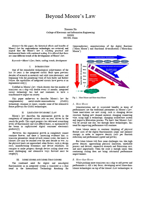
Beyond Moore’s LawXxxxxx XxCollege of Electronic and Information EngineeringXXXXXX XX, ChinaAbstract—In this paper, the historical effects and benefits of Moore’s law for semiconductor technologies are reviewed, and argue d that the Moore’s law is reaching practical and fundamental limits with continued scaling. It is offered that there are some different trends of the developments of Moore’s law.Keywords—Moore’s Law; limits; scaling; trends; developmentI.I NTRODUCTIONOne of the remarkable technological achievements of the last 50 years is the integrated circuit. Built upon previous decades of research in materials and solid state electronics, and beginning with the pioneering work of Jack Kilby and Robert Noyce, the capabilities of integrated circuits have grown at an exponential rate[1].Codified as Moore’s law, which decrees that the number of transistors on a chip will double every 18 months, integrated circuit technology has had and continues to have a transformative impact on society.This paper endeavors to describe Moore’s law for complementary metal–oxide–semiconductor (CMOS) technology, examine its limits, conider some of the alternative future pathways for CMOS technologies.II.L IMITATION O F M OORE’S L AWMoore’s law describes the exponentia l growth in the complexity of integrated circuits year on year, driven by the search for profit. This rapid progress has delivered astonishing levels of functionality and cost-effectiveness, as epitomized by the boom in sophisticated digital consumer electronics products[2].However, this exponential growth in complexity cannot continue forever, and there is increasing evidence that, as transistor geometries shrink towards atomic scales, the limits to Moore's law may be reached over the next decade or two. As the physical limits are approached, other factors, such as design costs, manufacturing economics and device reliability, all conspire to make progress through device scaling alone ever more challenging, and alternative ways forward must be sought[3].III.M ORE M OORE A ND M ORE-T HAN-M OORE The combined need for digital and non-digital functionalities in an integrated system is translated as a dual trend in the International Technology Roadmap for Semiconductors: miniaturization of the digital functions (“More Moore”) and functional diversification (“More-than-Moore”).Fig. 1.More Moore and More-than-MooreA.More MooreMiniaturization and its associated benefits in terms of performances are the traditional parameters in Moore’s Law. Some innovations are now rising, such as changing device structure, finding new channel material, changing connecting wire, using high k technology, changing architecture system and improve fabrication process. We know that Moore’s Law will be invalid one day, but through these technologies, this trend for improving performance will continue.More Moore means to continue shrinking of physical feature sizes of the digital functionalities (logic and memory storage) in order to improve density (cost per function reduction) and performance (speed and power).But More Moore will face some challenges too, like high power density, approaching physical limitation, unreliable process and devices, expensive research and fabrication cost, and most importantly, when the scale is enough small, then continuing scaling does not bring substantial performance improvements.B.More-than-MooreWhile packing more transistors on a chip to add power and performance is still a key focus, developing novel More-than-Moore technologies on top of the Moore's Law technologies toprovide further values to semiconductor chips has also becomea more important issue.More-than-Moore means that Incorporation into devices offunctionalities that do not necessarily scale according to “M oore’s L aw”, but provide addition al value in different ways.More-than-Moore approach allows for the non-digitalfunctionalities to migrate from the system board-level into thepackage (sip) or onto the chip (soc).The second trend is characterized by functionaldiversification of semiconductor-based devices. These non-digital functionalities do contribute to the miniaturization ofelectronic systems, although they do not necessarily scale at the same rate as the one that describes the development of digital functionality. Consequently, in view of added functionality, this trend may be designated “More-than-Moore” (MtM).But we will face some problems by using the technologies of More-than-Moore. Such as integration of More Moore with More-than-Moore and Creation of intelligent compact systems.More-than-Moore technologies cover a wide range of fields. For example, MEMS applications include sensors, actuators and ink jet printers. RF CMOS applications include Bluetooth, GPS and Wi-Fi. CMOS image sensors are found in most digital cameras. High voltage drivers are used to power LED lights. These applications add value to computing and memory devices that are made from the traditional Moore's Law technology.Fig. 2.2007 ITRS “Moore’s Law and More” Definition Graphic Proposal Fig.2 is a definition of “Moore’s Law and More”. The red part is More Moore and the blue part is More-than-Moore. The red part contains the computing and data storage logic, while the blue part contains RF, HH Power, Passives, Sensors, Actuators, Bio-chips, Fluidics and other functionalities.parisonComparing More Moore and More-than-Moore from Fig.3 and Fig.4, we can draw some conclusions:•More Moore has smallest footprint but limited functionality.•More-than-Moore has full functionality but complex supple chain.They all have advantages and disadvantages. We can use them according to specific application. Fig. 3.Following Moore’s Law is one approach:Monolithic CMOS logic System-on-ChipFig. 4.Adding More-than-Moore is another: System-on-Chip and System-in-PackageIn modern society, the concept of Internet of Things is verypopular. In the past, people may pay attention to computingand storage more, so the IC industry develops rapidly following Moore’s Law. But now, people pay more attention tointernet of things, biomedical and so on. That is to say, peopleneed more demands of the IC besides the computing andstorage functionality.Fig. 5.An ideal application of More-than-MooreFig.5 is an example of More-than-Moore, of course, it is anideal application. But it shows some benefits of this trend.IV.B EYOND C MOSA.What is Beyond CMOSWhat we have talked about before is all based on Si-based CMOS technology. But we should realize that Si-based CMOS technology cannot do everything, especially when the transistors continue shrinking of physical feature sizes towards atomic scale.Fig. 6.More Moore, More-than-Moore and Beyond CMOSWhat More Moore do is to continue to go forward along the road of “Moore’s Law”. And More-than-Moore do is to d evelop and extend “Moore’s Law”. When the scaling bellows about 10nm, traditional Si-based CMOS technology may be invalid. So what Beyond CMOS want to do is to invent new devices or technologies when Si-based CMOS comes across its limitation.Fig. 7.Some new devices and technologyThe main idea of Beyond CMOS is to invent one or several new type switches which can replace the Si-based CMOS to process information. So these ideal devices need to have higher function density, higher performance, less power consumption, acceptable manufacturing cost, stable enough and suitable for large-scale manufacturing and so on.B.Several new devices1)Tunneling FET(TFET)TFET mainly according to the principle of tunneling of quantum mechanics, directly goes through channel from the source to drain rather than by diffusion. Fig. 8.Tunneling FET(TFET)2)Quantum Cellular Automata (QCA)Representing the binary information by changing the structure of the Cellular.Transmitting information based on neighbor interaction.Fig. 9.Quantum Cellular Automata (QCA)Fig. 10.Quantum Cellular Automata (QCA)3)Atomic Switch(QCA)Atomic switch based on the formation and the annihilation of the metal atoms bridge between the two electrons, forming a gate-control switch mode.Fig. 11.Atomic Switch4)SpinFETSpinFET use the spinning direction of electron to carry information.Fig. 12.SpinFETFig. 13.SpinFETThey all have advantages or dis advantages. Maybe they are not the best devices, but they represent the potential development trend of the devices in the future[4].V.S UMMARYMicroelectronics therefore seeks to develop in new ways, not only to continue to deliver better performance in traditional markets, but also to grow into new markets based on devising new, non-electronic, functions on integrated circuits.Microelectronics relies on complementary metal oxide semiconductor (CMOS) technology, the backbone of the electronics industry. Beyond Moore's law, it is foreseen that microelectronics will be a platform to support optical, chemical and biotechnology to deliver a step change beyond electronics-only integration.R EFERENCES[1]Cavin R K, Lugli III P, Zhirnov V V. Science and engineering beyondMoore's law[J]. Proceedings of the IEEE, 2012, 100(Special Centennial Issue): 1720-1749.[2]Cumming D R S, Furber S B, Paul D J. Beyond Moore's law[J].Philosophical transactions. Series A, Mathematical, physical, and engineering sciences, 2014, 372(2012).[3]Saraswat K C. How far can we push Si CMOS and what are thealternatives for future ULSI[C]//Device Research Conference (DRC), 2014 72nd Annual. IEEE, 2014: 3-4.[4]Kazior T E. Beyond CMOS: heterogeneous integration of III–V devices,RF MEMS and other dissimilar materials/devices with Si CMOS to create intelligent microsystems[J]. Philosophical Transactions of the Royal Society of London A: Mathematical, Physical and Engineering Sciences, 2014, 372(2012): 20130105.。
精选半导体业生产计划

Purchasing
Supply Plan
Scheduling
Logistics
Planning
Order Mgmt
Demand Plan
Supply
Distribution
Production
Process Control
Manufacturing Execution System
Production Management: Current Status 生产管理现状
Solution (Resource: ITRS*)
解决方案(源自ITRS*)
Significant improvements in factory planning/scheduling are required. 必须通过先进生产计划和调度系统来提高半导体制造的生产率Improvements in factory forecasting and flexible factory information/control systems that can change with business conditions must be developed and implemented. 必须改进工厂的需求预测,建立柔性的工厂信息和管理软件系统,使得工厂产能可以随着市场环境的改变而改变… scheduling and dispatching… must be developed to improve equipment OEE and extendibility. 必须探索和发展生产调度和分派技术,以改进装备的利用率,提高工厂的可扩展性
Strategy
Plan
Execution
Supply Chain Management
Environmental guideline_Ashrae transaction

ABSTRACTRecent trends toward increased equipment power densityin data centers can result in significant thermal stress, with the undesirable side effects of decreased equipment availability,wasted floor space, and inefficient cooling system operation.In response to these concerns, manufacturers identified the need to provide standardization across the industry, and in 1998 a Thermal Management Consortium was formed. This was followed in 2002 by the creation of a new ASHRAE Tech-nical Group to help bridge the gap between equipment manu-fa cturers a nd fa cility designers a nd opera tors. “Therma l Guidelines for Data Processing Environments” the first publi-cation of TC9.9, is discussed in this paper, along with a histor-ical perspective leading up to the publication and discussion of issues that will define the roadmap for future ASHRAE activ-ities in this field.CURRENT INDUSTRY TRENDS/PROBLEMS/ISSUES Over the years, computer performance has significantly increased but unfortunately with the undesirable side effect of higher power. Figure 1 shows the National/International Tech-nology Roadmap for Semiconductors’ projection for proces-sor chip power. Note that between the years 2000 and 2005 the total power of the chip is expected to increase 60% and the heat flux will more than double during this same period. This is only part of the total power dissipation, which increases geometrically. The new system designs, which include very efficient interconnects and high-performance data-bus design,create a significant increase in memory and other device utili-zation, thus dramatically exceeding power dissipation expec-tations. As a result, significantly more emphasis has beenplaced on the cooling designs and power delivery methods within electronic systems over the past year.In addition, the new trend of low-end and high-end system miniaturization, dense packing within racks, and the increase in power needed for power conversion on system boards have caused an order of magnitude rack power increase. Similarly,this miniaturization and increase in power of electronics scales into the data center environment. I n fact, it wasn’t until recently that the industry has publicly recognized that the increasing density within the data center may have profound impact on the reliability and performance of the equipment it houses in the future. For this reason, there has been a recentflurry of papers addressing the need for new room coolingFigure 1Projection of processor power by the Na tiona l/Intern a tion a l Technology Ro a dm ap for Semiconductors.Evolution of Data Center Environmental GuidelinesRoger R. Schmidt, Ph.D.Christian BeladyAlan Classen Tom DavidsonMember ASHRAEAssociate Member ASHRAEMember ASHRAEMagnus K. Herrlin , Ph.D. Shlomo Novotny Rebecca PerryMember ASHRAERoger Schmidt and Alan Claassen are with IBM Corp., San Jose, Calif. Christian Belady is with Hewlett-Packard, Richardson, Tex. Tom Davidson is with DLB Associates, Ocean N.J. Magnus Herrlin is with ANCIS Incorporated , San Francisco, Calif.Shlomo Novotny and Rebecca Perry are with Sun Microsystems, San Diego, Calif.AN-04-9-1© 2004. American Society of Heating, Refrigerating and Air-Conditioning Engineers, Inc. (). Reprinted by permission from ASHRAE Transactions, Vol. 110, Part 1. This material may not be copied nor distributed in either paper or digital form without ASHRAE’s permission.technologies as well as modeling and testing techniques within the data center. All of these recognize that the status quo will no longer be adequate in the future. So what are the result-ing problems in the data center? Although there are many, the following list discusses some of the more relevant problems:1.Power density is projected to go upFigure 2 shows how rapidly machine power density is expected to increase in the next decade. Based on this figure it can easily be projected that by the year 2010server power densities will be on the order of 20,000 W/m 2. This exceeds what today’s room cooling infrastruc-ture can handle.2.Rapidly changing business demandsRapidly changing business demands are forcingT managers to deploy equipment quickly. Their goal is to roll equipment in and power on equipment immediately.This means that there will be zero time for site prepara-tion, which implies predictable system requirements (i.e.,“plug and play” servers).3.Infrastructure costs are risingThe cost of the data center infrastructure is rising rapidly with current costs in excess of about $1000/ft 2. For this reason, IT and facility managers want to obtain the most from their data center and maximize the utilization of their infrastructure. Unfortunately, there are many barri-ers to achieve this.First, airflow in the data center is often completely ad hoc.In the past, manufacturers of servers have not paid much attention to where the exhaust and inlets are in their equip-ment. This has resulted in situations where one server may exhaust hot air into the inlet of another server (some-times in the same rack). In these cases, the data center needs to be overcooled to compensate for this ineffi-ciency.In addition, a review of the industry shows that the envi-ronmental requirements of most servers from various manufacturers are all different, yet they all coexist in the same environment. As a result, the capacity of the datacenter needs to be designed for the worst-case server with the tightest requirements. Once again, the data center needs to be overcooled to maintain a problematic server within its operating range.Finally, data center managers want to install as many serv-ers as possible into their facility to get as much production as possible per square foot. In order to do this they need to optimize their layout in a way that provides the maxi-mum density for their infrastructure.The above cases illustrate situations that require over-capacity to compensate for inefficiencies.4.There is no NEBS equivalent specification for data centers.(NEBS [Network Equipment–Building Systems] is the telecommunication industry’s most adhered to set of phys-ical, environmental, and electrical standards and require-ments for a central office of a local exchange carrier.)IT/facility managers have no common specification that drives them to speak the same language and design to a common interface document.The purpose of this paper is to review what started as a “grassroots” industrywide effort that tried to address the above problems and later evolved into an ASHRAE Technical Committee. This committee then developed “Thermal Guide-lines for Data Processing Environments” (ASHRAE 2003a),which will be reviewed in this paper.HISTORY OF INDUSTRY SPECIFICATIONS Manufacturers Environmental Specifications In the late 1970s and early 1980s, data center site planning consisted mainly of determining if power was clean (not connected to the elevator or coffee pot), had an isolated ground, and if it would be uninterrupted should the facility experience a main power failure. The technology of the power to the equipment was considered the problem to be solved, not the power density. Other issues concerned the types of plugs,which varied widely for some of the larger computers.In some cases, cooling was considered a problem and, in some isolated cases, it was addressed in a totally different manner, so that the technology and architecture of the machine were dictated by the cooling methodology. Cray Research, for example, utilized a liquid-cooling methodology that forced a completely different paradigm for installation and rge cooling towers, which were located next to the main system, became the hallmark of computing prowess.However, typically the preferred cooling methods were simply bigger, noisier fans. The problem here was the noise and the hot-air recirculation when a system was placed too close to a wall.Over the last ten years, the type of site planning informa-tion provided has varied depending on the company's main product line. For companies with smaller personal computers or workstations, environmental specifications were much like those of an appliance: not much more than what is on the back of a blender. For large systems, worksheets for performingFigure 2Equipment power projection (Uptime Institute).calculations have been provided, as the different configura-tions had a tremendous variation in power and cooling require-ments.I n certain countries, power costs were a hugecontributor to total cost of ownership. Therefore, granularity, the ability to provide only the amount of power required for a given configuration, became key for large systems.In the late 1990s, power density became more of an issue and simple calculations could no longer ensure adequate cool-ing. Although cooling is a factor of power, this does not provide the important details of the air flow pattern and how the heat would be removed from the equipment. However, this information was vitally needed in equipment site planning guides. This led to the need for additional information, such as flow resistance, pressure drop, and velocity, to be available not only in the design stages of the equipment but after the release of the equipment for integration and support. This evolved into the addition of more complex calculations of the power spec-ifications, plus the airflow rates and locations, and improved system layouts for increased cooling capacity.In the early 2000s, power densities continued to increase as projected. Layout, based on basic assumptions, could not possibly create the efficiencies in the airflow that were required to combat the chips that were scheduled to be intro-duced in the 2004 time frame. Because of this, thermal model-ing, which was typically used to design products, began to be viewed as a possible answer for optimizing cooling in a data center environment. However, without well-designed thermal models from the equipment manufacturers and easy-to-use thermal modeling tools for facility managers, the creation or troubleshooting of a data center environment fell again to traditional tools for basic calculations to build a data center or to gather temperatures after a data center was in use.At this point it became apparent that the solution for rising heat densities could not be solved after the delivery of a prod-uct. Nor could it be designed out of a product during develop-ment. Instead, it had to be part of the architecture of the entire industry’s next-generation product offerings.Formation of Thermal Management Consortium In 1998 a number of equipment manufacturers decided to form a consortium to address common issues related to ther-mal management of data centers and telecommunications rooms. I nitial interest was expressed from the following companies: Amdahl, Cisco Systems, Compaq, Cray, Inc., Dell Computer, EMC, HP, BM, ntel, Lucent Technologies, Motorola, Nokia, Nortel Networks, Sun Microsystems, and Unisys. They formed the Thermal Management Consortium for Data Centers and Telecommunications Rooms. Since the industry was facing increasing power trends, it was decided that the first priority was to develop and then publish a trend chart on power density of the industry’s equipment that would aid customers in planning data centers for the future. Figure 2 shows the chart that resulted from this effort. This chart has been widely referenced and was published in collaboration with the Uptime Institute in 2000. Following this publication the consortium formed three subgroups to address what customers felt was needed to align the industry:A.Rack airflow direction/rack chilled airflow require-mentsB.Reporting of accurate equipment heat loadsmon environmental specificationsThe three subgroups worked on the development of guidelines to address these issues until an ASHRAE commit-tee was formed in 2002 that continued this effort. The result of these efforts is “Thermal Guidelines for Data Processing Envi-ronments” (ASHRAE 2003a), which is being published by ASHRAE. The objectives of the ASHRAE committee are to develop consensus documents that will provide environmental trends for the industry and guidance in planning for future data centers as they relate to environmental issues.Formation of ASHRAE GroupThe responsible committee for data center cooling within ASHRAE has historically been TC9.2, Industrial Air Condi-tioning. The 2003 ASHRAE Handbook—HVAC Applications, Chapter 17, “Data Processing and Electronic Office Areas”(ASHRAE 2003b) has been the primary venue within ASHRAE for providing this information to the HV AC indus-try. There is also Standard 127-2001, Method of Testing for Ra ting Computer a nd Da ta Processing Room Unita ry Air-Conditioners (ASHRAE 2001), which has application to data center environments.Since TC9.2 encompasses a very broad range of industrial air-conditioning environments, ASHRAE was approached in January 2002 with the concept of creating an independent committee to specifically address high-density electronic heat loads. The proposal was accepted by ASHRAE, and TG9.HDEC, High Density Electronic Equipment Facility Cooling, was created. TG9.HDEC's organizational meeting was held at the ASHRAE Annual Meeting in June 2002 (Hawaii). TG9.HDEC has since further evolved and is now TC9.9, Mission Critical Facilities, Technology Spaces, and Electronic Equipment.The first priority of TC9.9 was to create a thermal guide-lines document that would help to align the designs of equip-ment manufacturers and aid data center facility designers to create efficient and fault tolerant operation within the data center. The resulting document, “Thermal Guidelines for Data Processing Environments,” was completed in a draft version on June 2, 2003. I t was subsequently reviewed by several dozen companies representing computer manufacturers, facil-ities design consultants, and facility managers. Approval to submit the document to ASHRAE's Special Publications Section was made by TC9.9 on June 30, 2003, and the docu-ment publication is expected in December 2003.TC9.9 ENVIRONMENTAL GUIDELINESEnvironmental SpecificationsFor data centers, the primary thermal management focus is on the assurance that the housed equipment’s temperature and humidity requirements are being met. As an example, one large computer manufacturer has a 42U rack with front-to-rear air cooling and requires that the inlet air temperature into the front of the rack be maintained between 10°C and 32°C for elevations up to 1287 m (4250 feet). Higher elevations require a derating of the maximum dry-bulb temperature of 1°C for every 218 m (720 feet) above 1287 m (4250 feet) up to 3028 m (10000 feet). These temperature requirements are to be maintained over the entire front of the 2 m height of the rackwhere air is drawn into the system. These requirements can be a challenge for customers of such equipment, especially when there may be many of these racks arranged in close proximity to each other and each dissipating powers up to 12.5 kW when fully configured.As noted in the example above, data processing manufac-turers typically publish environmental specifications for the equipment they manufacture. The problem with these speci-fications is that other manufacturers with the same type of equipment and selling into the same customer environment may have a different set of environmental specifications. Not only do discrepancies occur between manufacturers; in some cases, there are discrepancies within the portfolio of a manu-facturer’s products. As one can imagine, customers of such equipment can be left in quandary as to what environment to provide in their data processing room.In an effort to standardize the environmental specifica-tions, the ASHRAE TC9.9 committee first surveyed the envi-ronmental specifications of a number of data processing equipment manufacturers. From this survey, four classes were developed that would encompass most of the specifications. Also included within the guidelines was a comparison to the NEBS specifications for the telecommunications industry to show both the differences and also aid in possible convergence of the specifications in the future.The four data processing classes cover the entire environ-mental range from air-conditioned server and storage environ-ments of classes 1 and 2 to the lesser controlled environments such as class 3 for workstations, PCs, and portables or class 4 for point-of-sales equipment with virtually no environmental control. For each class the allowable dry-bulb temperature, relative humidity, maximum dew point, maximum elevation, and maximum rate of change are specified for product oper-ating conditions. For higher altitudes, a derating algorithm is provided that accounts for diminished cooling. In addition to the allowable ranges, the recommended range for dry-bulb and relative humidity is provided for classes 1 and 2 based on the reliability aspects of the electronic hardware. Non-operating specifications of dry-bulb, relative humidity, and maximum dew point are also included.Finally, psychometric charts for all environmental classes including NEBS are provided in an Appendix of the guide. These are provided in both SI and IP units to aid the user of these charts. Both recommended (where appropriate) and allowable envelopes are provided for all classes.LayoutIn order for seamless integration between the server and the data center to occur, certain protocols need to be devel-oped, especially in the area of airflow. This section provides airflow guidelines for both the IT/facility managers and the equipment manufacturers to design systems that are compat-ible and minimize inefficiencies. To ensure this, the section covers the following items:1.Airflow within the cabinet2.Airflow in the facility3.Minimum aisle pitchIn order for data center managers to be able to design their equipment layouts, it is imperative that airflow in the cabinet be known. Currently, manufacturers design their equipment exhaust and inlets wherever it is convenient from an architec-tural standpoint. As a result, there have been many cases where the inlet of one server is directly next to the exhaust of adjacent equipment, resulting in the ingestion of hot air. This has direct consequences for the reliability of that machine. This guide attempts to steer manufacturers toward a common airflow scheme to prevent this hot air ingestion by specifying regions for inlets and exhausts. The guide recommends one of the three airflow configurations: front-to-rear, front-to-top, and front-to-top-and-rear as shown in Figure 3.Once manufacturers start implementing the equipment protocol, it will become easier for facility managers to opti-mize their layouts to provide maximum possible density by following the hot-aisle/cold-aisle concept. In other words, the front face of all equipment is always facing the cold aisle. Figure 4 shows how the inlets would line up.Finally, the guide addresses minimum practical aisle pitch for a computer room layout. Figure 5 shows a minimum 7 tile pitch where the tile could either be 24 inches or 600 mm.Table 1 shows how the space is allocated across the seventiles for either U.S. (24 in.) or Global (600 mm) tiles. Figure 3Recommended equipment airflow protocol.By following these guidelines, equipment manufacturers enable their customers to use the hot-aisle/cold-aisle protocol,which allows them to maximize the utilization of their data centers. In addition, as manufactures adopt the flow directions specified in the guidelines, the swapping out of obsolete serv-ers becomes much less problematic due to the uniform cooling direction.t is important to note that even if the guideline is followed, it does not guarantee adequate cooling. Although it will provide the best opportunity for success, it is still up to the facility manager to do the appropriate analysis to ensure cool-ing goals are met.Power Methodology and ReportingThe ASHRAE guide’s heat and airflow reporting section defines what information is to be reported by the information technology equipment manufacturer to assist the data center planner in the thermal management of the data center. The equipment heat release value is the key parameter that will be discussed in this section. Several other pieces of information are required if the heat release values are to be meaningful.These are included in the guide’s reporting section and are discussed briefly here.Currently, heat release values are not uniformly reported by equipment manufacturers and, as a result, site planners sometimes estimate equipment heat loads by using electricalinformation. Electrical information is always available because IEC 60950 (IEC 1999) and its USA and Canadian equivalent (CSA I nternational 2000) require the maximum power draw to be reported for safety purposes. The safety stan-dard requires rated voltage and current values to be placed on the equipment name-plate label. Electrical power and heat release are equivalent quantities for a unity power factor and are expressed in the same units (watts or Btu/h), but the name-plate electrical information is not appropriate for heat release estimation for data center thermal management purposes.The design guide states, “Name-plate ratings should at no time be used as a measure of equipment heat release.” The first reason is that the name-plate rating is only indicative of a worst-case maximum power draw. This maximum rating will often not be representative of the actual power draw for the equipment configuration to be installed. Second, there is no standard method for defining the maximum power draw.Equipment manufacturers are sometimes motivated to state high rating values so that safety certification current measure-ments at a rated voltage are well below the rated current. (The safety standard allows the measured current to exceed the rated value by 10%, but this is a situation that manufacturers naturally want to avoid.). The manufacturer may overstate or buffer the rating value to allow the use of higher power compo-nents in the future. If the data center planner starts with an inflated nameplate rating and then applies a factor to account for future power increases, the future increase has been counted twice. Third, multiplying a corresponding rated volt-age and current value results in a V A or kV A value that must be multiplied by a power factor, which may not be known, to get power in watts or Btu/h. While the power factor is a small adjustment for some modern equipment, not applying theTable 1. Aisle Pitch AllocationTile SizeAisle Pitch(cold aisle to cold aisle)1Nominal Cold Aisle Size2Max. Space Allocated forEquipment with No Overhang 3Hot Aisle Size U.S. 2 ft (610 mm)14 ft (4267 mm) 4 ft (1220 mm)42 in. (1067 mm) 3 ft (914 mm)Global600 mm (23.6 in.)4200 mm (13.78 ft)1200 mm (3.94 ft)1043 mm (41 in.)914 mm (3 ft)1If considering a pitch other than seven floor tiles, it is advised to increase or decrease the pitch in whole tile increments. Any overhang into the cold aisle should take into account the specific design of the front of the rack and how it affects access to the tile and flow through the tile.2Nominal dimension assumes no overhang, less if front door overhang exists.3Typically a one-meter rack is 1070 mm deep with the door and would overhang the front tile 3 mm for a U.S. configuration and 27 mm for global configuration.Figure 4Top view of a hot-aisle/cold-aisle configuration.Figure 5Minimum hot-aisle/cold-aisle configuration.power factor for other equipment may result in another cause of conservative heat load estimates.To avoid the above problems, the ASHRAE guide defines how heat release information should be determined and reported for data center thermal management purposes. The conditions used to determine the heat release values are spec-ified. They apply to all aspects of the process—measurement conditions, model conditions, and reporting conditions. The conditions are:•Steady stateValues based on peak currents are useful for power system design but not for data center thermal manage-ment.•All components in the active state, under significant stressThe intent is to avoid both unrealistically low values, such as an idle condition, and unrealistically high values.Significant stress in most power or safety test labs is more representative of normal customer operation, while the workload applied in a performance lab may represent a higher than normal workload. Words such as “worst-case” activity were specifically avoided. If heat release values were based on the unlikely condition of all compo-nents being in a worst-case activity state, the reported values would be excessively high and the resulting situa-tion would be similar to using name-plate rating values.•Nominal voltage input•Nominal ambient temperature from 20°C to 25°C (68°F to 77°F)This temperature range is the recommended operating temperature range for Class 1 and Class 2 in Table 2.1 of the ASHRAE document. At higher temperatures, air-moving devices may speed up and draw more power.Information technology equipment generally has multiple configurations. Heat release values are to be reported for configurations that span the range from mini-mum to maximum heat release values. It is acceptable thata heat release value be measured for every reportedconfiguration. It is also acceptable that a predictive model be developed and validated to provide heat release values for multiple configurations. The model would allow the manufacturer to report heat release values for more configurations than could be practically measured.During equipment development, there may be a period when no heat release measurements are available. During this time the model would be based solely on predictions.The ASHRAE document states, “measured values must be factored into the model by the time the product is announced.” Appropriate values are measured by the equipment manufacturers as part of the safety certifica-tion process, which requires the manufacturer to make electrical measurements. Heat release model validation involves comparing values predicted by the model with measured heat release values for the same configurations.The number of tested configurations is not specified, but the required accuracy is defined: the predicted values must be within 10% of the measured values or the model must be adjusted.Besides heat release values, equipment manufacturers must report additional information for each configuration: •Description of configuration•Dimensions of configurationDividing the heat release value by the equipment foot-print allows the data center planner to calculate the heat load density in W/m2 or W/ft2.•Weight for configurationThis is not directly used for thermal management.However, the weight might result in the equipment being spaced apart to meet floor loading requirements. This would result in a decreased heat density, which is impor-tant to know for data center thermal management.•Minimum/maximum airflow characteristics of each con-figuration in cubic feet per minute (cfm) and cubic meters per hour (m3/h)Unlike the heat release values, which are based on a nominal ambient temperature range, some systems may exhibit variable flow rates due to fan control, which can be dependent upon ambient temperature. For each load-ing condition, flow rate is to be reported along with the ambient temperature relative to that flow rate. The ambi-ent temperature range should be reflective of the temper-ature that produces the minimum flow rate as well as the ambient temperature that produces the maximum flow rate. Presumably these temperatures would reflect the allowable ambient extents for which the hardware is designed. The airflow is also reported with all air-moving devices operating normally. For example, if a fan is only powered when another unit fails, the auxiliary unit should be off when determining the airflow value to be reported.•Airflow diagramThis can be a simple outline of the equipment showing where the airflow enters and leaves the unit. In the future it may be necessary to provide more information. For example, each inlet and exit airflow arrow may need to be associated with a volumetric airflow value, and the exit airflow arrows may also require a number indicating how much heat the airflow picked up while in the equipment.The goal would be to represent the equipment as a compact model in a data center thermal model.An example report is included in the guide. It conveys many important aspects of the information to be reported, but it may not be complete for a given product. The example report provides information for minimum, full, and typical configu-rations. The words “maximum” and “average” configuration were specifically avoided; average particularly may be defined several different ways. I t is hoped that the typical configuration used for thermal management purposes will be the same typical configuration used for acoustic measure-。
Chemical-Reviews-ALD-Overview-Jan-2010

Atomic Layer Deposition:An OverviewSteven M.George*Department of Chemistry and Biochemistry and Department of Chemical and Biological Engineering,University of Colorado,Boulder,Colorado80309Received February12,2009 Contents1.Introduction1112.Al2O3ALD as a Model ALD System1123.Thermal and Plasma or Radical-Enhanced ALD1133.1.Thermal ALD1133.2.Plasma or Radical-Enhanced ALD1144.Reactors for ALD1155.Metal ALD Using Thermal Chemistry1165.1.Fluorosilane Elimination Chemistry116bustion Chemistry1175.3.Hydrogen Reduction Chemistry1176.Nucleation and Growth during ALD1186.1.Metal Oxide ALD on H-Si(100)1186.2.Metal ALD on Oxide Surfaces1186.3.Al2O3ALD on Carbon Nanotubes andGraphene Surfaces1197.Low Temperature ALD1197.1.Al2O3ALD and Other Metal Oxide ALD1197.2.Catalytic SiO2ALD1208.ALD on Polymers1219.ALD on High Aspect Ratio Structures12210.ALD on Particles12311.ALD of Nanolaminates and Alloys12412.Polymer MLD125anic Polymers12512.2.Hybrid Organic-Inorganic Polymers12613.Additional Topics12713.1.Nonideal ALD Behavior and the ALD Window12713.2.Area-Selective ALD for Spatial Patterning12713.3.Atmospheric Pressure ALD12713.4.ALD on Biological Templates12813.5.Other Emerging Areas12814.Conclusions12815.Acknowledgments12916.References129 1.IntroductionAtomic layer deposition(ALD)has emerged as an important technique for depositing thinfilms for a variety of applications.Semiconductor processing has been one of the main motivations for the recent development of ALD. The International Technology Roadmap for Semiconductors (ITRS)has included ALD for high dielectric constant gate oxides in the MOSFET structure and for copper diffusion barriers in backend interconnects.1In addition,ALD has met challenging requirements in other areas including the deposi-tion of high quality dielectrics to fabricate trench capacitors for DRAM.2Miniaturization in the semiconductor industry has led to the requirement for atomic level control of thinfilm deposition.Miniaturization has produced very high aspect structures that need to be coated conformally.No other thin film technique can approach the conformality achieved by ALD on high aspect structures.The necessity for continuous and pinhole-freefilms in semiconductor devices has driven the advancement of ALD.Other applications with similar demanding requirements outside of the semiconductor in-dustry are low electron leakage dielectrics for magnetic read/ write heads3and diffusion barrier coatings with low gas permeability.4*E-mail address:Steven.George@.Steven M.George is Professor in the Department of Chemistry andBiochemistry and Department of Chemical and Biological Engineering atthe University of Colorado at Boulder.Dr.George received his B.S.inChemistry from Yale University(1977)and his Ph.D.in Chemistry fromthe University of California at Berkeley(1983).Prior to his appointmentsat the University of Colorado at Boulder,Dr.George was a BantrellPostdoctoral Fellow at Caltech(1983-4)and an Assistant Professor inthe Department of Chemistry at Stanford University(1984-1991).Dr.George is a Fellow of the American Vacuum Society(2000)and a Fellowof the American Physical Society(1997).He has also received theAmerican Chemical Society Colorado Section Award(2004),R&D100Award for Particle-ALD(2004),NSF Presidential Young Investigator Award(1988-1993),and an Alfred P.Sloan Foundation Fellowship(1988).Dr.George’s research interests are in the areas of surface chemistry,thinfilm growth,and nanostructure engineering.He is currently directing aresearch effort focusing on atomic layer deposition(ALD)and molecularlayer deposition(MLD).This research is examining new surface chemistriesfor ALD and MLD growth,measuring thinfilm growth rates,andcharacterizing the properties of thinfilms.Dr.George served as Chair ofthefirst American Vacuum Society(AVS)Topical Conference on AtomicLayer Deposition(ALD2001)held in Monterey,California.He also teachesa one-day short course on ALD for the AVS.Dr.George is a cofounderof ALD NanoSolutions,Inc.,a startup company that is working tocommercialize ALD technology.Chem.Rev.2010,110,111–13111110.1021/cr900056b 2010American Chemical SocietyPublished on Web11/30/2009ALD is able to meet the needs for atomic layer control and conformal deposition using sequential,self-limiting surface reactions.A schematic showing the sequential,self-limiting surface reactions during ALD is displayed in Figure 1.5Most ALD processes are based on binary reaction sequences where two surface reactions occur and deposit a binary compound film.Because there are only a finite number of surface sites,the reactions can only deposit a finite number of surface species.If each of the two surface reactions is self-limiting,then the two reactions may proceed in a sequential fashion to deposit a thin film with atomic level control.The advantages of ALD are precise thickness control at the Ångstrom or monolayer level.The self-limiting aspect of ALD leads to excellent step coverage and conformal deposition on high aspect ratio structures.Some surface areas will react before other surface areas because of different precursor gas fluxes.However,the precursors will adsorb and subsequently desorb from the surface areas where the reaction has reached completion.The precursors will then proceed to react with other unreacted surface areas and produce a very conformal deposition.The self-limiting nature of the surface reactions also produces a nonstatistical deposition because the randomness of the precursor flux is removed as an important factor.As a result,ALD films remain extremely smooth and conformal to the original substrate because the reactions are driven to completion during every reaction cycle.6Because no surface sites are left behind during film growth,the films tend to be very continuous and pinhole-free.This factor is extremely important for the deposition of excellent dielectric films.7ALD processing is also extendible to very large substrates and to parallel processing of multiple substrates.The ALD precursors are gas phase molecules,and they fill all space independent of substrate geometry and do not require line-of-sight to the substrate.ALD is only limited by the size of the reaction chamber.The ALD process is also dominated by surface reactions.Because the surface reactions are performed sequentially,the two gas phase reactants are not in contact in the gas phase.This separation of the two reactions limits possible gas phase reactions that can form particles that could deposit on the surface to produce granular films.The use of the term “ALD”dates back approximately to 2000.Prior to 2000,the term atomic layer epitaxy (ALE)was in common use.8-13Other terms have been used to describe ALD,including binary reaction sequence chemis-try 14and molecular layer epitaxy.15The transition from ALEto ALD occurred as a result of the fact that most films grown using sequential,self-limiting surface reactions were not epitaxial to their underlying substrates.Moreover,amorphous films were most preferred for dielectric and diffusion barrier applications.Consequently,the use of ALD grew in prefer-ence and now dominates with the practitioners in the field.The history of ALE and ALD dates back to the 1970s in Finland.The original pioneer of ALE was Tuomo Suntola,who demonstrated some of the first ALE processes as early as August/September 1974.16The first ALE system devel-oped was ZnS.16The first ALE patent emerged in 1977.17The first literature paper on ALE appeared in 1980in Thin Solid Films.18The first application of ALE was electrolu-minescent displays.The first public display of an ALE device was an electroluminescent display that operated in the Helsinki airport from 1983to 1998.The first commercial ALE reactor was the F-120sold by Microchemistry in 1988.The first of a series of ALE meetings was held in 1990and continued through 1996.The first of a series of yearly ALD meetings was held in 2001and has continued through the present date.Many earlier reviews have addressed the basics of ALE or ALD.5,8,11,12,19-21Many previous reviews have considered the application of ALE or ALD to microelectronics and nanotechnology.19,22-27The intent of this present review is not to duplicate these previous reviews.Instead,this review is focused on an overview of key concepts and new directions in ALD.The semiconductor roadmap is coming to an end in a few years because of the limits of the current electronic materials.For continued progress,the future for electronic materials will embrace as yet undefined paradigms.ALD will almost certainly be part of the new paradigms because of its ability to control deposition on the atomic scale and to deposit conformally on very high aspect ratio structures.2.Al 2O 3ALD as a Model ALD SystemThe ALD of Al 2O 3has developed as a model ALD system.An earlier extensive review by Puurunen has previously discussed the details of Al 2O 3ALD.20Consequently,this section will only mention the highlights of Al 2O 3ALD.Al 2O 3ALD is usually performed using trimethylaluminum (TMA)and H 2O.The first reports of Al 2O 3ALD using TMA and H 2O date back to the late 1980s and early 1990s.28,29More recent work in the semiconductor industry is using TMA and ozone for Al 2O 3ALD.30,31This review will concentrate on Al 2O 3ALD using TMA and H 2O.The surface chemistry during Al 2O 3ALD can be described as5,14,32where the asterisks denote the surface species.The Al 2O 3ALD growth occurs during alternating exposures to TMA and H 2O.Al 2O 3ALD is a model system because the surface reactions are very efficient and self-limiting.The main driver for the efficient reactions is the formation of a very strong Al -O bond.The overall reaction for Al 2O 3ALDisFigure 1.Schematic representation of ALD using self-limiting surface chemistry and an AB binary reaction sequence.(Reprinted with permission from ref 5.Copyright 1996American Chemical Society.)(A)AlOH*+Al(CH 3)3f AlOAl(CH 3)2*+CH 4(1)(B)AlCH 3*+H 2O f AlOH*+CH 4(2)2Al(CH 3)3+3H 2O f Al 2O 3+3CH 4∆H )-376kcal(3)112Chemical Reviews,2010,Vol.110,No.1GeorgeThis reaction has an extremely high reaction enthalpy.33This is one of the highest reaction enthalpies encountered for any ALD reaction.The potential energy surfaces during Al 2O 3ALD have been modeled using density functional theory (DFT).34These calculations show that Al(CH 3)3exists in a deep precursor well complexed to AlOH*species prior to its surface reaction,as shown in Figure 2.34Likewise,the calculations show that H 2O is also in a deep precursor well complexed to AlCH 3*species prior to its surface reaction.These complexes result from strong Lewis acid -base interactions on the surface.Although these precursor wells have not been experimentally observed,they may be fairly general for various classes of ALD reactions.The surface chemistry of Al 2O 3ALD has been confirmed by in situ FTIR studies.32,35,36The FTIR difference spectra clearly show the loss of AlOH*species and concurrent gain of AlCH 3*species during the TMA reaction.Likewise,the loss of AlCH 3*species and the concurrent gain of AlOH*species is observed during the H 2O reaction.The gas phase reaction products during Al 2O 3ALD have also been identi-fied using quadrupole mass spectrometry studies.37,38Using Al(CH 3)3and D 2O as the reactants,CH 3D was observed as the main reaction product,as expected from the surface chemistry for Al 2O 3ALD.37By repeating the surface reactions,Al 2O 3growth is extremely linear with the number of AB cycles.14,39Various techniques,such as spectroscopic ellipsometry and quartz crystal microbalance (QCM)measurements,have character-ized the growth per cycle during Al 2O 3ALD.Typical measured Al 2O 3ALD growth rates are 1.1-1.2Åper AB cycle.14,39The resulting Al 2O 3ALD films are smooth and extremely conformal to the underlying substrate.Studies on nanoparticles show excellent conformality of Al 2O 3ALD films.35,40,41Investigations on high aspect ratio trench sub-strates also reveal superb conformality,as illustrated by the cross-sectional scanning electron microscopy (SEM)image in Figure 3.42One of the hallmarks of ALD is self-limiting surface chemistry.The self-limiting surface reactions during Al 2O 3ALD have been observed by in situ FTIR 32,35and QCM 39investigations as well as by spectroscopic ellipsometry studies.14The reactant exposures required for the surfacereactions to reach completion reveal that the reactive sticking coefficients during Al 2O 3ALD are much less than unity.Based on required exposure times,the reactive sticking coefficients are in the range of ∼10-3-10-4during Al 2O 3ALD.14The growth per one ALD cycle is also much smaller than one Al 2O 3“monolayer”.The growth rates of 1.1-1.2Åper AB cycle can be compared with the thickness of one Al 2O 3“monolayer”.This monolayer thickness is estimated using the density of 3.0g/cm 3for Al 2O 3ALD films grown at 177°C.43Based on this density,the number density of “Al 2O 3”units is F )1.77×10²²Al 2O 3units/cm 3.The number of Al 2O 3units per square centimeter is equal to F 2/3)6.8×1014cm -2.Likewise,the monolayer thickness is equal to F -1/3)3.8Å.The growth per AB cycle of 1.1-1.2Åper AB cycle is much less than this estimate of the monolayer thickness.The disagreement between growth per AB cycle and the monolayer thickness is not surprising because ALD growth is dependent on surface species and surface chemistry.This surface chemistry is not required to always yield a “mono-layer”of growth during every AB cycle.The correlation between ALD growth and surface chemistry is clearly illustrated by the temperature-dependence of Al 2O 3ALD growth per AB cycle.The growth per AB cycle decreases progressively with temperature between 177and 300°C.This decrease results from the progressive loss of AlOH*and AlCH 3*surface species at higher temperatures.14,32The continuous and pinhole-free nature of Al 2O 3ALD films is revealed by their superb electrical properties.Current -voltage curves for various Al 2O 3ALD film thick-nesses on n-Si(100)reveal electrical behavior that is very similar to that of thermal SiO 2films.7The Al 2O 3ALD films have a dielectric constant of ∼7and display very low electron leakage.7Increases in the current density versus applied potential occur as a result of Fowler -Nordheim tunneling.This characteristic is consistent with the absence of any defects or pinholes in the Al 2O 3ALD film.These excellent properties have enabled Al 2O 3ALD films to serve as gate oxides and to passivate semiconductor surfaces.44-463.Thermal and Plasma or Radical-Enhanced ALD 3.1.Thermal ALDALD is closely related to chemical vapor deposition (CVD)based on binary reactions such as A +B fProduct.Figure 2.Reaction path and predicted energetics for reactions of Al(CH 3)3on the Al -OH*surface site calculated using the Al(OAl(OH)2)2-OH cluster.The structures are shown using the Al(OH 2)-OH cluster for clarity.(Reprinted with permission from ref 34.Copyright 2002American Institute ofPhysics.)Figure 3.Cross-sectional SEM image of an Al 2O 3ALD film with a thickness of 300nm on a Si wafer with a trench structure.(Reprinted with permission from ref 42.Copyright 1999John Wiley &Sons.)Atomic Layer Deposition Chemical Reviews,2010,Vol.110,No.1113For CVD using binary reactions,the A and B reactants are present at the same time and form the productfilm continu-ously on the substrate.In ALD,the substrate is exposed to the A and B reactants individually and the productfilm is formed in a stepwise and very digital fashion.A generic recipe for ALD is tofind a CVD process based on a binary reaction and then to apply the A and B reactants separately and sequentially in an ABAB...binary reaction sequence. There are many examples of ALD resulting from binary reaction CVD processes.Examples for TiO2and ZnO are based on the following binary CVD reactions and their corresponding reaction enthalpies:33These ALD systems yield a growth per AB cycle of∼0.4Åfrom150to600°C for TiO2ALD47and2.2-2.5Åfrom 100to160°C for ZnO ALD.48,49These ALD chemistries have negative heats of reaction and are robust ALD reactions. These reactions occur spontaneously at various temperatures and will be referred to as thermal because they can be performed without the aid of plasma or radical assistance.A survey of developed ALD processes reveals that most thermal ALD systems are binary compounds based on binary reactant CVD.20,21The most common thermal ALD systems are binary metal oxides such as Al2O3,TiO2,ZnO,ZrO2, HfO2,and Ta2O5.Other common thermal ALD systems are binary metal nitrides such as TiN,TaN,and W2N.Thermal ALD systems also exist for sulfides such as ZnS and CdS and phosphides such as GaP and InP.3.2.Plasma or Radical-Enhanced ALDThere is also a need for single-element ALD materials, such as metals and semiconductors,that can be deposited using a binary reaction sequence.Except for some notable exceptions discussed in section5,the single-elementfilms of metals and semiconductors are very difficult to deposit using thermal ALD processes.Fortunately,these single-elements can be deposited using plasma or radical-enhanced ALD.22The radicals or other energetic species in the plasma help to induce reactions that are not possible using just thermal energy.Plasma sources can be used to generate hydrogen radicals that reduce the metal or semiconductor precursors.Hydrogen radicals can also be produced using a hot tungstenfilament.A scheme for metal ALD using metal reactants and hydrogen radicals is shown in Figure4. Hydrogen radical-enhanced ALD wasfirst demonstrated for Ti ALD50using a H2plasma.Ta ALD is another ALD system that has been studied extensively using hydrogen radicals from H2plasmas.51The reactants for Ta ALD are TaCl5and hydrogen radicals.51The surface chemistry for Ta ALD can be expressed asTaCl5isfirst exposed to the surface.Subsequently,the hydrogen radicals reduce the Ta atoms and remove the chlorine from the surface.Although the growth per cycle during Ta ALD is only0.08Åper AB cycle,the Ta ALD films have excellentfilm resistivities and show good Cu barrier properties.51The small growth per cycle is attributed to steric hindrance caused by the large TaCl5admolecule on the surface.XRD also indicates that the Ta ALDfilm is -Ta and has very small nanograins.51The limitations of hydrogen radical-enhanced ALD were also demonstrated by studies using trenched samples.51The Ta ALDfilms were not conformal in trenches with a high aspect ratio of40:1.When the Ta ALDfilm had a thickness of28nm at the top of the trench,the thickness was only11 nm at the bottom of the trench.The lower Ta ALD growth at the bottom of the trench is attributed to hydrogen radical recombination on the walls of the trench that attenuates the hydrogen radicalflux.52Radical recombination will limit the general utility of plasma ALD in high aspect ratio structures. The ALD of single-element semiconductors such as Si and Ge can also be deposited using hydrogen radical-enhanced ALD.The surface chemistry for Si ALD is based on the desorption kinetics for H2,HCl,and SiCl2from silicon surfaces.H2desorbs at535°C,53,54HCl desorbs at575°C,53 and SiCl2desorbs at725°C53,55during temperature pro-grammed desorption(TPD)experiments from silicon sur-faces.H2desorbs at a lower temperature than HCl from silicon surfaces.SiCl2desorbs at a higher temperature than HCl from silicon surfaces.Consequently,silicon can be deposited using a chlorine-containing silicon precursor such as SiH2Cl2.The surface chemistry for Si ALD using SiH2Cl2and hydrogen radicals can be written asAt the appropriate temperature,H2and HCl will desorb upon SiH2Cl2adsorption but SiCl2will not desorb from the silicon surface.The build up of chlorine on the silicon surface will produce a self-limiting adsorption of SiH2Cl2.The surface chlorine can then be removed by exposing the surface to hydrogen radicals.The hydrogen radicals add hydrogen atoms to the silicon surface that recombine with surface chlorine to desorb as HCl or with other surface hydrogen atoms to desorb as H2.The hydrogen radicalflux will eventually remove all the surface chlorine species. Studies of Si ALD using SiH2Cl2and H radicals have demonstrated the self-limiting nature of Si ALD growth versus both SiH2Cl2and hydrogen radical exposures.56,57A Si ALD growth per cycle of∼1.6Åwas observed betweenTiO2ALD:TiCl4+2H2O f TiO2+4HCl∆H)-16kcal(4)ZnO ALD:Zn(CH2CH3)2+H2O f ZnO+2C2H6∆H)-70kcal(5)(A)Ta*+TaCl5f TaTaCl5*(6)(B)TaCl5*+5H·f Ta*+5HCl(7)Figure4.Schematic diagram of hydrogen radical-enhanced ALDusing a metal reactant and hydrogen radicals.(A)Si*+SiH2Cl2f SiSiCl2*+H2(8)(B)SiCl2*+2H f Si*+2HCl(9)114Chemical Reviews,2010,Vol.110,No.1George550and610°C.At higher temperatures,the Si ALD growth per cycle increased as a result of Si CVD.At lower temperatures,the Si ALD growth per cycle decreased as a result of incomplete surface reactions.A similar strategy was also applied for Ge ALD using GeH2Cl2and hydrogen radicals.58,59Si and Ge ALD were both demonstrated on silicon and germanium surfaces.However,a difficulty with Si and Ge ALD is their nucleation on other types of surfaces.Si and Ge are both very reactive and easily react with oxygen from oxide substrates to form SiO2or metals from metallic substrates to form silicides.Consequently,the nucleation of Si and Ge ALD is very difficult.The nucleation problems have limited the surface chemistry for Si and Ge ALD to only silicon and germanium surfaces.In addition to single-element materials,plasma-enhanced ALD can deposit compound materials.One important advantage is that plasma-enhanced ALD can depositfilms at much lower temperatures than thermal ALD.For example, plasma-enhanced Al2O3ALD can be performed using TMA and O2plasma at temperatures as low as room temperature.60 The low temperature deposition is useful for coating thermally fragile substrates such as polymers.61The plasma-enhanced Al2O3ALDfilms also have improved electrical properties compared with thermal Al2O3ALD62and lead to excellent passivation of silicon substrates.63Plasma-enhanced ALD has also been useful to deposit metal nitrides,such as TiN and TaN,which generally cannot be grown with high quality using organometallic precursors.64 TaN ALD has been achieved using organometallic tantalum precursors such as terbutylimidotris(diethylamido)tantalum (TBTDET)and hydrogen radicals.60,65,66The plasma-enhanced process can form TaNfilms that have much lower electrical resistivity and higher density than TaN ALDfilms grown using thermal TaN ALD with TBTDAT and NH3.67,68 Oxygen radical-enhanced ALD has been employed to grow metal oxides using metal -diketonate precursors.Metal oxides,such as Y2O3,have been grown at low temperatures with minimal carbon contamination.69Remote O2plasmas have also been utilized for plasma enhanced Pt ALD with (methylcyclopentadienyl)trimethylplatinum as the metal pre-cursor.70In addition,plasma-enhanced Ru ALD has been accomplished using bis(ethylcyclopentadienyl)ruthenium and NH3plasma.71These plasma-enhanced Ru ALDfilms have potential as adhesion layers for copper interconnects.65 4.Reactors for ALDThere are different types of ALD reactors.Many ALD reactor designs were discussed in the original patents by T. Suntola in197717and1983.72Various ALD reactors and design principles were also described in early reviews of ALE by T.Suntola.12,13,73One of the early ALD reactors had a revolving substrate holder that rotated the substrate in and out of the A and B reactantflow streams.Another design was based on gasflow through hot wall CVD tube reactors. Other ALD reactorsflowed the reactant in an inert carrier gas through a small channel between the reactor wall and substrate.This design was known as the“traveling-wave”reactor and is represented by the F-120reactor by Micro-chemistry Ltd.11To organize the various ALD reactor designs,there are two limiting types of ALD reactors that can be defined by the pumping and use of a carrier gas.In one limit are ALD reactors where the reactants are exposed without using a carrier gas and sometimes with throttled pumping.14,15,74Afterthe exposures,the reactants are removed by opening upcompletely to the pump and evacuating the reactor.Becauseof the long residence times in the reactor,these exposurescan utilize reactants very efficiently.However,the evacuationtimes for these ALD reactors can be slow in the absence ofa purge gas.At low pressures in molecularflow,the randomwalk of molecules colliding only with the reactor walls leadsto long pumping times.In another limit are ALD reactors where the reactants areexposed with a carrier gasflowing through the reactor.12,39,75The carrier gas is in viscousflow andflows continuously tothe pump.If the reactants have sufficient vapor pressure,thereactants can be dosed into the carrier gas stream.Alterna-tively,the carrier gas canflow over the headspace of a solidor liquid reactant or through the liquid reactant if the reactanthas a lower vapor pressure.The carrier gas entrains thereactants and products and defines a short residence time inthe reactor.The advantage of the viscousflow reactors istheir much shorter ALD cycle times relative to the ALDreactors employing no carrier gas during reactant exposureand purging.Most ALD reactors operate with an inert carrier gas inviscousflow.The optimum pressure for viscousflow reactorsis around∼1Torr.This optimum pressure is a trade-offbetween gas interdiffusion and entrainment.For example,the interdiffusion coefficient of O2in N2is D12)132cm2/sat1Torr and0°C.This interdiffusion coefficient isdetermined knowing that D12)0.174cm2/s at1atm and0°C76and that gas diffusion is inversely proportional to pressure,D∼1/P.76The mean squared displacement,x2,resulting from gas diffusion is x2)6Dt,where t is time.Therefore,the mean displacement for O2in N2gas at1Torrand0°C is x)28cm in1s.This sizable mean displacementindicates that diffusion of reactants in N2gas at1Torr issufficient for removal of reactants and products from stagnantgas in the reactor in a reasonable time.The pressure of1Torr is also high enough for the N2tobe an effective carrier gas.The mean free path,λ,betweenN2molecules at room temperature isλ∼5×10⁻³cm/P,where P is in Torr.77This approximation reveals that themean free path of N2at1Torr isλ∼50µm.This smallmean free path indicates that N2gas is in viscousflow at1Torr and will effectively entrain reactants.Mean displace-ments may be too small for effective purging from stagnantgas at pressures higher than1Torr.Entrainment will be lesseffective at pressures lower than1Torr when the gas meanfree paths are longer.Inert carrier gas pressures around∼1Torr are a compromise between these two factors.One ALD reactor that optimizes the residence times duringreaction and purging is known as synchronously modulatedflow and draw(SMFD).78The SMFD design injects the inertflowing gas at the reactor inlet during the purge steps and atthe reactor outlet during the reactant exposures.The syn-chronized modulation of the inertflowing gas between thereactor inlet and the reactor outlet enables high-speed gasflow switching.A schematic illustrating the dose and purgemodes during SMFD is shown in Figure5.79The reactant has a long residence time during dosing andonly experiences a slow“draw”from the inertflowing gasentering at the reactor outlet.The reactant can be utilizedvery efficiently during the dose mode.In contrast,the reactanthas a short residence time during the purge mode becauseinert carrier gas enters at the reactor inlet andflows throughAtomic Layer Deposition Chemical Reviews,2010,Vol.110,No.1115。
碳纳米管的羧基化
Carbon-Nanotube-Templated andPseudorotaxane-Formation-Driven Gold NanowireSelf-AssemblyToby Sainsbury and Donald Fitzmaurice*Department of Chemistry,University College Dublin,Belfield,Dublin4,Ireland Received December22,2003.Revised Manuscript Received March15,2004A cation-modified multiwalled carbon nanotube is used to template the noncovalent self-assembly in solution of a gold nanowire from crown-modified gold nanoparticles.The driving force for self-assembly is formation of the surface-confined pseudorotaxane that results from the electron-poor cation threading the electron-rich crown.IntroductionThe demand for integrated circuits that will allow information to be processed at even faster speeds remains undiminished.This is despite the fact that the density of the wires and switches that comprise such circuits has doubled every eighteen months for nearly four decades,giving rise to Moore’s Law.1It is clear that Moore’s Law will hold true until2012; it is not clear that it will hold true thereafter.2The responses of the relevant technological and scientific communities have been two-fold:first,to continue to develop existing fabrication and materials technologies; and second,to consider alternative fabrication and materials technologies.When considering alternative fabrication technolo-gies,one is attracted to the self-assembly in solution and self-organization at a conventionally patterned silicon wafer substrate of nanoscale wires and switches.3 When considering alternative materials technologies, one is attracted to the use of the growing number of nanoscale condensed-phase and molecular building blocks that are becoming available.4Specifically,one is attracted to the use of nanoscale condensed-phase and molecular building blocks to self-assemble in solution and self-organize at a patterned silicon wafer substrate metal nanowires.5It was in this context that Fullam et al.previously reported the multiwalled carbon nanotube(MWNT) templated self-assembly of gold nanowires from gold nanoparticles.6Briefly,unmodified MWNTs added to a stable dispersion of tetraoctylammonium bromide (TOAB)-modified gold nanoparticles templated the as-sembly in solution of gold nanowires comprised of discrete gold nanoparticles.It was suggested that the driving force for self-assembly was charge transfer from the conduction band states of the gold nanoparticle to theπ*states of the carbon nanotubes.7It is noted that there has been a large number of subsequent reports describing the preparation of metal-and metal-oxide-coated carbon nanotubes.8It is also noted that there has been a large number of reports describing the chemical modification of carbon nano-tubes.Initially,these reports focused on the covalent introduction of carboxy groups at the surface of the carbon nanotubes.9Subsequently,these reports have focused on the covalent coupling of an increasingly wide range of functional molecules and biomolecules to the surface of carboxy-modified carbon nanotubes.10 Reported herein is the preparation of cation-modified (dibenzylammonium)MWNTs and crown-modified(di-benzo[24]crown-8)gold nanoparticles(Scheme1).It was expected that the above cation-modified MWNTs would*To whom correspondence should be addressed.E-mail: donald.fitzmaurice@ucd.ie.(1)Moore,G.Electronics1965,38,114.(2)International Technology Roadmap for Semiconductors,2002 (/).(3)Parviz,B.;Ryan,D.;Whitesides,G.IEEE Trans.Adv.Pac.2003, 26,233.(4)Parak,W.;Gerion,D.;Pellegrino,T.;Zanchet,D.;Micheel,C.; Williams,S.;Boudreau,R.;Le Gros,M.;Larabell,C.;Alivisatos,A. Nanotechnology2003,14,15.(5)Richter,J.Physica E2003,16,157.(6)Fullam,S.;Rensmo,H.;Cottell,D.;Fitzmaurice,D.Adv.Mater. 2000,12,1430.(7)(a)Brust,M.;Kiely,C.;Bethell,D.;Schiffrin,D.J.Am.Chem. Soc.1998,120,12367.(b)Maxwell,A.;Bruhwiler,P.;Nilsson,A.; Martensson,N.Phys.Rev.B1994,49,10717.(c)Hunt,M.;Modesti, S.;Rudolf,P.;Palmer,R.Phys.Rev.B1995,51,10039.(8)(a)Satishkumar,B.;Vogl,E.;Govindaraj,A.;Rao,C.J.Phys. D:Appl.Phys.1996,29,3173.(b)Zhang,Y.;Franklin,N.;Chen,R.; Dai,H.Chem.Phys.Lett.2000,331,35.(c)Banerjee,S.;Wong,S.Nano Lett.2002,2,195.(d)Li,Y.;Ding,J.;Chen,J.;Cailu,X.;Wei,B.;Liang, J.;Wu,D.Mater.Res.Bull.2002,1847,1.(e)Azamian,B.;Coleman, K.;Davis,J.;Hanson,N.;Green,mun.2002,366.(f) Fu,Q.;Lu,C.;Liu,J.Nano Lett.2002,2,329.(g)Choi,H.;Shim,M.; Bangsaruntip,S.;Dai,H.J.Am.Chem.Soc.2002,124,9058.(h) Haremza,J.;Hahn,M.;Krauss,T.;Chen,S.;Calcines,J.Nano Lett. 2002,2,1253.(i)Han,W.-Q.;Zettl,A.J.Am.Chem.Soc.2003,125, 2062.(j)Ellis,A.;Vijayamohanan,K.;Goswami,R.;Chakrapani,N.; Ramanathan,L.;Ajayan,P.;Ramanath,G.Nano Lett.2003,3,279. (k)Jiang,K.;Eitan,A.;Schadler,L.;Ajayan,P.;Siegel,R.;Grobert, N.;Mayne,M.;Reyes-Reyes,M.;Terrones,H.;Terrones,M.Nano Lett. 2003,3,275.(l)Ravindran,S.;Chaudhary,S.;Colburn,B.;Ozkan, M.;Ozkan,C.Nano Lett.2003,3,447.(m)Han,W.-Q.;Zettl,A.Nano Lett.2003,3,681.(9)(a)Hiura,H.Mol.Cryst.Liq.Cryst.1995,267,267.(b)Hiura,H.;Ebbesen,T.;Tanigaki,K.Adv.Mater.1995,7,275.(c)Ebbesen, T.;Hiura,H.;Bisher,M.;Tracey,M.;Shreeve-Keyer,J.;Haushalter, R.Adv.Mater.1996,8,155.(d)Dujardin,E.;Ebbesen,T.;Krishnan, A.;Treacy,M.Adv.Mater.1998,10,611.(e)Burghard,M.;Krstic,V.; Duesberg,G.;Philipp,G.;Muster,J.;Roth,S.Synth.Met.1999,103, 2540.(f)Satishkumar,B.;Govindaraj,A.;Mofokeng,J.;Subbanna, G.;Rao,C.J.Phys.B:At.Mol.Opt.1996,29,4925.(g)Dillon,A.; Gennett,T.;Jones,K.;Alleman,J.;Parilla,P.;Heben,M.Adv.Mater. 1999,11,1354.2174Chem.Mater.2004,16,2174-217910.1021/cm035368k CCC:$27.50©2004American Chemical SocietyPublished on Web05/01/2004template the noncovalent self-assembly in solution of a gold nanowire from the above crown-modified gold nanoparticles(also Scheme1).This expectation was based on the fact that the electron-poor cation threads the electron-rich crown insolution to form a pseudorotaxane.11This expectation was also based on the fact that cation-modified silica and crown-modified silver nanoparticles self-assemble in solution,and that self-assembly is driven by forma-tion of the corresponding surface-confined pseudorotax-ane.12Experimental MethodsAll solvents and compounds were used as supplied by the Sigma-Aldrich Chemical Co.Ltd.,unless otherwise stated.Visible absorption spectra were recorded using a HP-8452A spectrophotometer with LabView software written to acquire the data.All visible absorption spectra were recorded against appropriate solvent or solution backgrounds.All TEMs were obtained using a JEOL2000FX TEMscan (at an accelerating voltage of80kV)for samples deposited on both uncoated(2000mesh)and carbon-coated(400mesh) copper grids.The preparation of samples for TEM analysis involved the deposition of a drop of the relevant sample onto the above grids.The excess sample was removed by wicking and the grid was allowed to dry in air.Preparation of Unmodified and Crown-Modified Gold Nanoparticles.A stable dispersion of dodecanethiol-modified gold nanoparticles was prepared in chloroform using a method similar to that described by Brust et al.13These nanoparticles were size-selectively precipitated to isolate a relatively size-monodisperse fraction(7.7nm diameter,polydispersity1.13). The near size-monodisperse fraction was subsequently modi-fied by exchange of the adsorbed thiol for a thiol incorporating a crown.The above exchange was promoted using a method similar to that described by Ahern et al.14Purification of Unmodified MWNTs.As-received MWNTs (MER Corporation,3×10-3g)were suspended by sonication (15min)in chloroform(20mL).The resulting suspension was centrifuged(5000rpm,15min)and the supernatant fraction (approximately75vol%)was retained.This procedure was repeated a further three times,with the supernatant fraction being retained in each case.Preparation of Carboxy-Modified MWNTs.MWNTs were treated as described following the method reported by Burghard et al.to introduce carboxy groups at the surface of the nanotubes.15This was achieved by refluxing the as-received MWNTs in nitric acid to produce hydroxyl,carbonyl, and carboxy groups at defects in the nanotube carbon lattice. The above hydroxyl and carbonyl groups were further oxidized to carboxy groups by treatment of the oxidized MWNTs with potassium permanganate and perchloric acid as described below.Specifically,MWNTs(3.2×10⁻³g)were added to nitric acid (3mL,69wt%)and sonicated to ensure they were dispersed. The resulting suspension of MWNTs was refluxed under magnetic stirring(4h,130°C)to oxidize the suspended MWNTs.The oxidized suspension of MWNTs was cooled and filtered using a polycarbonate membrane(Whatman-UK,0.2-µm pore diameter)and washed with deionized water(200mL). The oxidized MWNTs retained on the membrane were dis-persed in deionized water(10mL)by sonication.An acidic solution of potassium permanganate(9×10⁻³g,5.7×10-5 mol)and perchloric acid(3mL,50wt%)was then added to the stirring solution.The potassium permanganate was quenched after10min by the addition of a solution of citric acid(0.133g,6.3×10-4mol).The suspension was filtered using a polycarbonate membrane(Whatman-UK,0.2-µm pore diameter)and washed with deionized water(200mL).The resulting carboxy-modified MWNTs(3.0×10⁻³g)were dispersed in deionized water(10mL)by sonication.TEMs of the MWNTs were obtained before and after the above oxidative process.A drop of one of the following suspensions was deposited onto a carbon-coated copper grid: unmodified MWNTs(3×10⁻³g)in chloroform(10mL),or carboxy-modified MWNTs(3×10⁻³g)in water(10mL).Preparation of Cation-Modified MWNTs.The required cation-precursor,N-(4-carboxydibenzylamine)carbamate6-(10)(a)Huang,W.;Lin,Y.;Taylor,S.;Gaillard,J.;Rao,A.;Sun, Y.-P.Nano Lett.2002,2,231.(b)Huang,W.;Taylor,S.;Fu,K.;Lin, Y.;Zhang,D.;Hanks,T.;Rao,A.;Sun,Y.-P.Nano Lett.2002,2,311.(c)Pompeo,F.;Resasco,D.Nano Lett.2002,2,369.(d)Shim,M.;Wong Shi Kam,N.;Chen,R.;Li,Y.;Dai,H.Nano Lett.2002,2,285.(e)Kahn, M.;Banerjee,S.;Wong,S.Nano Lett.2002,2,1215.(f)Frehill,F.; Vos,J.;Benrezzak,S.;Koos,A.;Konya,Z.;Ruther,M.;Blau,W.; Fonseca,A.;Nagy,J.;Biro,L.;Minett,A.;in het Panhuis,M.J.Am. Chem.Soc.2002,124,13694.(g)Star,A.;Liu,Y.;Grant,K.;Ridvan, L.;Stoddart, F.;Steuerman, D.;Diehl,M.;Boukai, A.;Heath,J.Macromol.2003,36,553.(h)Stevens,J.;Huang,A.;Peng,H.;Chiang, I.;Khabashesku,V.;Margrave,J.Nano Lett.2003,3,331.(i) Chambers,G.;Carroll,C.;Farrell,G.;Dalton,A.;McNamara,M.;in het Panhuis,M.;Byrne,H.Nano Lett.2003,3,843.(j)Besteman,K.; Lee,J.-O.;Wiertz,F.;Heering,H.;Dekker,C.Nano Lett.2003,3,727.(11)(a)Ashton,P.;Campbell,P.;Chrystal,E.;Glink,P.;Menzer, S.;Philp,D.;Spencer,N.;Stoddart,J.;Tasker,P.;Williams,D.Angew. Chem.Intl.Ed.Engl.1995,17,1865.(b)Ashton,P.;Fyfe,M.; Hickingbottom,S.;Menzer,S.;Stoddart,J.;White,A.;Williams,D. Chem.Eur.J.1998,4,577.(12)(a)Fitzmaurice,D.;Rao,S.;Preece,J.;Stoddart,J.;Wenger, S.;Zaccheroni,N.Angew.Chem.Intl.Ed.1999,38,1147.(b)Ryan, D.;Rao,S.;Rensmo,H.;Fitzmaurice, D.;Preece,J.;Wenger,S.; Stoddart,J.;Zaccheroni,N.J.Am.Chem.Soc.2000,122,6252.(13)Brust,M.;Walker,M.;Bethell,D.;Schiffrin,D.;Whyman,R. mun.1994,801.(14)Ahern,D.;Rao,S.;Fitzmaurice,D.J.Phys.Chem.B.1999, 103,1821.(15)Burghard,M.;Krstic,V.;Duesberg,G.;Philipp,G.;Muster, J.;Roth,S.Synth.Met.1999,103,2540.Scheme1.A Cation-Modified Multiwalled CarbonNanotube Templates the NoncovalentSelf-Assembly in Solution of a Gold Nanowire fromCrown-Modified Gold NanoparticlesSelf-Assembly of Gold Nanowire Using MWNTs Chem.Mater.,Vol.16,No.11,20042175nitroveratryloxy chloroformate,was prepared as described in detail elsewhere.16Modification of the MWNTs required two amide-coupling reactions:the first was between carboxy-modified MWNTs and ethylenediamine,and the second was between the re-maining amine of the coupled ethylenediamine and the cation-precursor,as described below.Specifically,ethylenediamine (5.6×10⁻⁶mL,8.3×10-4mol)was added,followed by EDAC (1.91×10⁻¹g,1×10-3mol)and DMAP (12×10-3g,1×10-4mol),to a suspension of carboxy-modified MWNTs (3×10⁻³g)in water (10mL),and the resulting suspension was stirred for 12h.The sus-pension was filtered on a polycarbonate membrane (Whatman-UK,0.2-µm pore diameter)and washed with deionized water (200mL).The above membrane was sonicated in deionized water (10mL)to recover the modified MWNTs.The water was removed using a rotary evaporator,which was followed by drying on a vacuum line (3h).The modified MWNTs were dispersed in anhydrous di-chloromethane (10mL)by sonication.The cation-precursor (10.6×10⁻³g,2.3×10-5mol),followed 30s later by EDAC (20×10-3g,1.0×10-4mol)and DMAP (1.30×10⁻³g,1.0×10-5mol),was added to the stirred suspension of the above modified MWNTs.The suspension was stirred for 16h in a sealed flask in the absence of light.The material was filtered using an Anodisc filter membrane (Whatman-UK,0.02-µm pore diameter),and washed with anhydrous dichloromethane (100mL)followed by ethanol (100mL).The above membrane was sonicated in ethanol (10mL)to recover the cation-precursor-modified MWNTs.The output from a UV-H 253BL Ultra Violet 250-W UV lamp was used as the light source for photoactivation.Hexa-fluorophosphoric acid was added to a suspension of cation-precursor-modified-MWNTs (3×10⁻³g)in ethanol (10mL)until the pH was 2.The suspension was irradiated using the UV lamp for 2h,filtered on a polycarbonate membrane (Whatman-UK,0.2-µm pore diameter),and washed with ethanol (100mL).This procedure results in the photoactivated deprotection of the dibenzylamine in acidic conditions in the presence of a counterion,PF 6-.The resultant salt of thedibenzylammonium cation (cation)is formed.The cation-modified MWNTs were dispersed by sonication in ethanol (10mL).The ethanol was removed by rotary evaporation followed by drying on a vacuum line (3h).The dry cation-modified MWNTs were dispersed by sonication in chloroform (10mL).Templated Self-Assembly of Gold Nanowires.The templated self-assembly of gold nanowires from these compo-nents is described in detail in the Results and Discussion section of this paper and therefore is not described in this section.Results and DiscussionPreparation and Characterization of Cation-Modified MWNTs.A TEM of the as-received MWNTs reveals that there is a significant amount of amorphous carbon present (Figure 1a).To remove this impurity,the above MWNTs were sonicated in chloroform,cen-trifuged,and filtered.A TEM of the purified MWNTs shows a well-dispersed sample with an average nano-tube diameter of 24nm and an average nanotube length of 2µm (Figure 1b).The oxidation of MWNTs under strongly acidic condi-tions results in the introduction of carboxylic,hydroxyl,and carbonyl groups at defect sites on the surface of the MWNTs in the approximate ratio 4:2:1(Scheme 2).9a -d To maximize the number of functional groups suitable(16)(a)Ryan,D.;Nagle,L.;Rensmo,H.;Fitzmaurice,D.J.Phys.Chem.B .2002,106,5371.(b)Ryan,D.;Nagle,L.;Fitzmaurice,D.Nano Lett.,published online Mar.18,2004,/10.1021/nl0351340.Figure 1.As-received multiwalled carbon nanotubes (a)prior to purification,(b)following purification,and (c and d)following carboxy-modification.Scheme 2.Introduction of Carboxyl,Hydroxy,and Carbonyl Groups at the Defect Sites Present at the Surface of the As-Received Multiwalled Carbon Nanotubes Followed by Conversion of Carbonyland Hydroxy Groups to Carboxy Groups2176Chem.Mater.,Vol.16,No.11,2004Sainsbury and Fitzmauricefor covalent modification,the above hydroxy and car-bonyl groups were subsequently oxidized to carboxy groups (Scheme 2).9e It is estimated that the density of carboxy groups present at the surface of the above carboxy-modified MWNT is 4.2per 100Å2.This esti-mate is based on findings reported by Hiura and co-workers,concerning the number of carbon atoms at the surface of a known mass of MWNTs,9a and by Rao et al.,concerning the number of carboxy groups present following acid oxidation of a known mass of MWNTs.9f A TEM of the carboxy-modified MWNTs shows a well-dispersed material with an average diameter of 24nm and an average length of 2µm (Figure 1c and d).The cation-precursor (N -(4-carboxydibenzylamine)-carbamate-6-nitroveratryloxy chloroformate)was co-valently coupled to the surface of the carboxy-modified MWNTs.Because the carboxy-modified MWNTs and cation precursor both have carboxy moieties,ethylene-diamine was deemed a suitable linker.Coupling was achieved by EDAC-catalyzed amide formation between the carboxy-modified MWNTs and ethylenediamine,and between ethylenediamine and the carboxy group of the cation precursor (Scheme 3).To minimize the possibility of cross-linking of MWNTs,the amount of ethylenedi-amine used was in excess of the number of carboxy groups present at the surface of the MWNTs.No aggregation of the MWNTs was observed before or after the above reaction.The surface density of attached molecules in the resulting cation-precursor-modified MWNTs was estimated to be 2.7per 100Å2,assuming a yield of 80%for each amide formation step.The cation-modified MWNT-templated self-assembly of crown-modified gold nanoparticles requires the priordeprotection of the cation precursor under acidic condi-tions to form the cation.This is achieved by photolysis of the cation precursor in the presence of hexafluoro-phosphoric acid.Preparation and Characterization of Modified Gold Nanoparticles.Briefly,thiol-modified (do-decanethiol)gold nanoparticles were prepared using a method similar to that reported by Brust et al .13These nanoparticles were selectively precipitated to isolate a relatively size-monodisperse fraction.These nanopar-ticles were further modified by exchange of the initially adsorbed thiol molecules for crown-thiol molecules (dodecane thiol incorporating a crown moiety in the terminal position).14A TEM analysis of 200nanopar-ticles yields an average diameter of 7.7nm and a polydispersity of 1.13(Figure 2).Visible absorption spectroscopy confirmed the exist-ence of the characteristic absorbance maximum at 520nm,which was assigned to the surface plasmon reso-nance of the gold nanoparticles.Templated Self-Assembly of Gold Nanowires.To initiate the templated self-assembly of a gold nanowire in solution,a dispersion of crown-modified gold nano-particles (0.2mL,4×1012nanoparticles mL -1)in chloroform was added to a freshly sonicated suspension of cation-modified MWNTs (0.5mL,15×10-5g mL -1)also in chloroform.Following equilibration of this suspension for 24h a black precipitate was obtained.TEM analysis revealed the formation of gold nanowires (Figure 3a).A series of related control experiments was performed under similar conditions.Specifically,a dispersion of crown-modified gold nanoparticles (0.2mL,4×1012nanoparticles mL -1)in chloroform was added to a freshly sonicated suspension of cation-precursor-modified MWNTs (0.5mL,15×10-5g mL -1)also in chloroform.Following equilibration of this suspension for 24h no black precipitate was observed.TEM analy-sis revealed no gold nanowire formation (Figure 3b).A dispersion of crown-modified gold nanoparticles (0.2mL,4×1012nanoparticles mL -1)in chloroform was added to a freshly sonicated suspension of unmodified MWNTs (0.66mL,11×10-5g mL -1)also in chloroform.Following equilibration of this suspension for 24h no black precipitate was observed.TEM analysis revealed no gold nanowire formation (Figure 3c).A dispersion of thiol-modified gold nanoparticles (0.2mL,4×1012nanoparticles mL -1)in chloroform was added to a freshly sonicated suspension of cation-modified MWNTs (0.5mL,5×10-5g mL -1)also in chloroform.Following equilibration of this suspensionScheme 3.Covalent Coupling of One End of the Ethylenediamine Linker to a Carbonyl Group Present at the Surface of a Carboxy-Modified Multiwalled Nanotube Followed by Coupling of the Other End of the Linker to the CationPrecursorFigure 2.Crown-modified gold nanoparticles.Self-Assembly of Gold Nanowire Using MWNTs Chem.Mater.,Vol.16,No.11,20042177for 24h no black precipitate was observed.TEM analysis revealed no gold nanowire formation (Figure 3d).A further series of control experiments was also performed under similar conditions.A dispersion of crown-modified gold nanoparticles (0.2mL,4×1012nanoparticles mL -1)in chloroform was added to a freshly sonicated suspension of cation-modified MWNTs (0.66mL,11×10-5g mL -1)also in chloroform,in the presence of an excess of free cation (dibenzylammonium hexafluorophosphoric acid,3.3×10-3g,9.5×10-6mol).Following equilibration of this suspension for 24h no black precipitate was observed.TEM analysis revealed no gold nanowire formation (Figure 3e).Also,a dispersion of crown-modified gold nano-particles (0.2mL,4×1012nanoparticles mL -1)in chloroform was added to a freshly sonicated suspension of cation-modified MWNTs (0.66mL,11×10-5g mL -1)also in chloroform,in the presence of an excess of free crown (dibenzo24-crown-8,4.3×10-3g,9.5×10-6mol).Following equilibration of this suspension for 24h no black precipitate was observed.TEM analysis revealed no gold nanowire formation (Figure 3f).It is clear from these findings that MWNT-templated self-assembly of a gold nanowire is observed only when uncomplexed cation is present on the surface of the MWNTs and uncomplexed crown is present at the surface of the gold nanoparticle.On this basis it may be concluded that the templated self-assembly of nano-wires is driven by formation of the surface-confined pseudorotaxane shown in Scheme 1.The fact that coverage of the MWNT by the adsorbed gold nanoparticles is complete would suggest that the coverage of cation at the surface of the cation-modified MWNTs is extensive.It is estimated that each molecule adsorbed at the surface of a cation-modified MWNT occupies an area of 6.1×6.1Å.9On the basis that the projected area of a crown-modified nanoparticle within 15Å(the length of an adsorbed cation)of the MWNT is 1461Å2,it is further estimated that each particle is in contact with up to 40cations,consistent with the high degree of coverage observed.The possibility that the driving force for the templated nanowire assembly is charge transfer from the crown-modified nanoparticle to the cation-modified MWNT can be excluded.This assertion is supported by the findingsFigure 3.Transmission electron micrographs of (a)crown-modified gold nanoparticles adsorbed at the surface of a cation-modified multiwalled carbon nanotube.The same gold nanoparticles are not adsorbed at the surface of (b)a cation-precursor-modified multiwalled carbon nanotube or (c)an unmodified multiwalled carbon nanotube.Similarly,(d)thiol-modified gold nanoparticles (prior to exchange of thiol incorporating)are not adsorbed at a cation-modified multiwalled carbon nanotube.Crown-modified gold nanoparticles are not adsorbed at the surface of cation-modified multiwalled carbon nanotubes in the presence of (e)free cation or (f)free crown in solution.2178Chem.Mater.,Vol.16,No.11,2004Sainsbury andFitzmauricethat there is no adsorption of crown-modified gold nanoparticles at cation-precursor-modified MWNTs or cation-modified MWNTs in the presence of added crown, both of which would be expected to exhibit similar degrees of steric hindrance to cation-modified MWNTs.ConclusionsThis paper describes the use of a dibenzylammonium-cation-modified multiwalled carbon nanotube to tem-plate the noncovalent self-assembly of a gold nanowire in solution from dibenzo[24]crown-8-modified gold nano-particles.The driving force for self-assembly is forma-tion of a surface-confined pseudorotaxane.By exploiting these capabilities and insights,allied to those recently reported in relation to the patterning of nanoparticles14,17and those that will be reported in relation to the carbon-nanotube-templated self-assembly of other nanoparticles,18it ought be possible to pattern nanotubes by the adsorption of a range of nanoparticles. This,in turn,will offer the prospect of diverse nanoscale components for which many applications can be foreseen. CM035368K(17)(a)Nagle,L.;Ryan,D.;Cobbe,S.;Fitzmaurice,D.Nano Lett.2003,3,51.(b)Nagle,L.;Fitzmaurice,D.Adv.Mater.2003,15,933.(c)Ryan,D.;Nagle,L.;Cobbe,S.;Fitzmaurice,D.International PCTApplication,2002,application PCT/IE02/00120.(18)Sainsbury,T.;Fitzmaurice,D.unpublished findings.Self-Assembly of Gold Nanowire Using MWNTs Chem.Mater.,Vol.16,No.11,20042179。
国际半导体技术发展路线图_ITRS(英文)-2015

INTERNATIONAL TECHNOLOGY ROADMAP
FOR
SEMICONDUCTORS 2.0
2015 EDITION
EXECUTIVE REPORT
THE ITRS 2.0 IS DEVISED AND INTENDED FOR TECHNOLOGY ASSESSMENT ONLY AND IS WITHOUT REGARD TO ANY COMMERCIAL CONSIDERATIONS PERTAINING TO INDIVIDUAL PRODUCTS OR EQUIPMENT.
2015 ITRS 2.0 ACKNOWLEDGMENTS
INTERNATIONAL ROADMAP COMMITTEE Europe—Mart Graef, Bert Huizing, Reinhard Mahnkopf Japan— Hidemi Ishiuchi, Yoshihiro Hayashi, Nobuyuki Ikumi, Hiroyuki Miyakawa Korea—Siyoung Choi, Jae Hoon Choi, Taiwan—Sam Pam, Wilman Tsai U.S.A.—Paolo Gargini, Taffy Kingscott, Linda Wilson
TECHNOLOGY WORKING GROUP KEY CONTRIBUTORS
2015 Cross TWG Study Group (Technology Pacing)—Alan Allan, Dave Armstrong, An Chen, Mustafa Badaroglu, Joel Barnett, Roger Barth, Herbert Bennett, Bill Bottoms, Juan-antonio Carballo, Carlos Diaz, Alain Diebold, Paul Feeney, Mike Gaitan, Paolo Gargini, Mike Garner, Hidemi Ishiuchi, Dan Herr, Hirofumi Inoue, Scott Jones, Andrew Kahng, Leo Kenny, Rich Liu, Jürgen Lorenz, Steve Moffat, James Moyne, Mark Neisser, Kwok Ng, George Orji, Lothar Pfitzner, Gopal Rao, Thomas Skotnicki, Hitoshi Wakabayashi, Mike Walden, Linda Wilson, Osamu [Sam] Yamazaki, Victor Zhirnov, Paul Zimmerman
静电控制的发展趋势

关于静电控制,国际半导体技术发展报告(International Technology Roadmap for Semiconductors,简称ITRS)ITRS 2003指出:“静电在半导体生产的各个环节都会产生不利影响,导致三类基本问题。
1、静电吸附(ESA)污染会随着尘粒的变小而显得越发严重,使得要达到缺陷密度目标变得越发地困难。
2、静电放电(ESD)会对设备和光掩模都造成不利影响。
设备尺寸特征的减小,意味着一个静电放电只需要更少的电能就可以对组件和掩模产生破坏。
3、由于ESD及相关的电磁干扰(EMI)而导致的设备故障会降低OEE(总体设备效率)。
而随着设备微处理器的运行速度的加快,这一切的发生也变得越来越频繁。
这三种问题在以下地方都会发生:生产芯片和光掩模的地方,芯片工厂中生产组件的地方,以及在封装、测试等后道工序中生产独立组件的地方。
ITRS还包含了一些如何减少静电荷的建议,以达到预防静电问题的标准。
在新的设施建设中、在新设备中,以及在现存的加工厂中都应该采纳这些建议。
因为随着更新、更小技术的引进,静电的防护标准也必须相应提高,所以,在每一个半导体加工厂中都执行一套静电控制程序就显得非常重要。
由静电问题而造成的损失,会比执行这些静电控制程序所需费用高十倍,甚至一百倍。
ITRS 2003推荐在建立和检验静电控制程序时,使用两个国际半导体设备和材料协会(Semiconductor Equipment and Materials International,简称SEMI)的标准。
E78-1102“半导体设备静电释放(ESD)与静电吸附(ESA)评估和控制指南”,对设备生产过程中的静电控制提出建议,描述了为了保护免受静电危害而设置的产品静电灵敏度标准及其测量方法。
这一条款最初是在1998年发布,后来考虑到半导体技术快速发展的要求,作了一些相应的修改。
SEMI发布的最新的文件是E129-1103:“对半导体生产设施的静电控制评估指南。
- 1、下载文档前请自行甄别文档内容的完整性,平台不提供额外的编辑、内容补充、找答案等附加服务。
- 2、"仅部分预览"的文档,不可在线预览部分如存在完整性等问题,可反馈申请退款(可完整预览的文档不适用该条件!)。
- 3、如文档侵犯您的权益,请联系客服反馈,我们会尽快为您处理(人工客服工作时间:9:00-18:30)。
COMPARISON OF SUPER VISED LEARNING METHODS FOR SPIKE TIME CODING IN SPIKING NEURAL NETWORKSANDRZEJ KASIŃSKI,FILIP PONULAKAbstract.In this review we focus our attention on the supervised learning methods for spiketime coding in Spiking Neural Networks(SNN).This study is motivated by the recent experi-mental results on information coding in the biological neural systems which suggest that precisetiming of individual spikes may be essential for efficient computation in the brain.We pose a fundamental question,what paradigms of neural temporal coding can be imple-mented with the recent learning methods.In order to answer this question we discuss various approaches to the considered learning task.We shortly describe the particular learning algorithms and report the results of experiments.Finally we discuss properties,assumptions and limitations of each method.We complete thisreview with a comprehensive list of pointers to the literature.1.IntroductionFor many years a common belief was that the essential information in neurons is encoded in theirfiring rates.However,recent neurophysiological results suggest that efficient processing of information in neural systems can be founded also on the precise timing of action potentials (spikes)([1,2,3]).In the barn owl auditory system,neurons detecting coincidence receive volleys of precisely timed spikes from both ears([4,5]).Under the influence of a common oscillatory drive in the rat hippocampus,the strength of a constant stimulus is coded in the relative timing of neuronal action potentials([6]).In humans precise timing offirst spikes in tactile afferents encodes touch signals at thefinger tips([1]).Time codes have also been suggested for rapid visual processing([1]).Precise temporal coding paradigm is required in some artificial control systems.Examples are neuroprosthetic systems which aim at producing a functionally useful movements of the paralysed limbs by exciting muscles or nerves with the sequences of short electrical impulses([7]).Precise relative timing of impulses is critical for generating the desired,smooth movement trajectories.In addition to aforementioned examples,it has been theoretically demonstrated that the tem-poral neural code is very efficient whenever the fast processing of information is required([8]).All these arguments provide strong motivation for investigating the computational properties of the systems that compute with precisely timed spikes.It is generally agreed that artificial Spiking Neural Networks(SNN)([4,9,10])are capable of exploiting time as a resource for coding and computation in a much more sophisticated manner than typical neural computational models([11,12]).SNNs appear to be an interesting tool for investigating the temporal neural coding and for exploiting its computational potential.Although significant progress has already been made to recognize information codes that can be beneficial for computation in SNN([4,9,11,13]),it is still an open problem to determine efficient neural learning mechanisms that enable implementation of these particular time-coding schemes.Unsupervised spike-based learning methods,such as LTP,LTD and STDP have already been widely investigated and described in the literature([14,15,16,17,18,19,20]).However,unsuper-vised approach is not suitable to the learning tasks that require an explicit goal definition.In this article we focus on supervised learning methods for precise spike timing in SNN.The goal of our study is to determine what paradigms of neural information coding can be implemented with the recent approaches.Date:27.10.2005.Key words and phrases.Supervised Learning,Spiking Neural Networks,Time Coding,Temporal Sequences of Spikes.The work was partially supported by the State Committee for Scientific Research,project1445/T11/2004/27.12ANDRZEJ KASIŃSKI,FILIP PONULAKFirst,we present the supervised learning methods for spike timing,which are known from the literature.We classify these methods to more general groups representing particular learning approaches and shortly describe each of the learning algorithms.Finally,we summarize main facts about the learning approaches and discuss their properties.2.Review of Learning MethodsIn this section we present some representative methods for supervised learning in SNN.For all these methods the common goal of learning can be stated as follows:Given a sequence of input spikes trains S in (t )and a sequence of the target output spikes S d (t ),find vector of synaptic weights w ,such that outputs of learning neurons S out (t )are close to S d (t ).2.1.Methods based on gradient evaluation.Learning in the traditional,artificial neural networks (ANN)is usually performed by gradient ascent techniques ([21]).However,explicit evaluation of gradient in SNN is infeasible due to discontinuous-in-time nature of spiking neurons.Indirect approaches or special simplifications must be assumed to deal with this problem.In ([22,23])Bohte and colleagues presented one of such approaches.Their method,called Spike-Prop ,is analogous to the backpropagation algorithm ([24])known from the traditional Artificial Neural Networks.The target of SpikeProp is to learn a set of desired firing times,denoted t d j ,at the postsynapticneurons j ∈J for a given set of input patterns S in (t ).Each neuron in a simulated network isallowed to fire only once during a single simulation cycle.The learning method is based on an explicit evaluation of the gradient of E =1/2 j (t d j −t out j )2with respect to the weights of each synaptic input to j (where t out j is an actual firing time of neuron j ).To overcome the discontinuous nature of spiking neurons,authors approximated the thresholding ly,it was assumed that for a small region around t =t out j ,thefunction V m j (t ),denoting the membrane potential of j ,could be linearly approximated.On thisassumption error-backpropagation equations were derived for a fully connected feedforward network with hidden layers.SpikeProp algorithm has been re-investigated in ([25,26,27,28]).It was found that the weight initialization is a critical factor for a good performance of the learning rule.In ([25])the weights were initialized with the values that led the network to the successful training in a similar number of iterations as in ([22]),but with large learning rates,although Bohte argued that the approxi-mation of the threshold function implies that only small learning rates can be used ([23]).Other experiments of Moore ([25])also provided evidence that negative weights could be allowed and still led to successful convergence,which was in contradiction to the conclusions of Bohte.Xin and Embrechts ([27])proposed a modification of the learning algorithm by including the momentum term in the weight update equation.It has been demonstrated that this modification significantly speeded up the convergence of SpikeP rop .In ([26])additional learning rules were introduced for the synaptic delays,time constants and for the neurons’thresholds.This resulted with smaller network topologies and also with faster algorithm convergence.Finally,Tiňo and Mills ([28])ex-tended SpikeProp to recurrent network topologies,to account for the temporal dependencies in the input stream.Neither the original SpikeProp method nor any of the proposed modifications enable learning of patterns composed of more than one spike per neuron.Properties of the SpikeProp method were demonstrated in a set of classification experiments.These included standard and interpolated XOR problem ([13]).SpikeProp authors encoded the input and output values by time delays,associating the analog values with the corresponding “earlier”or “later”firing times.In the interpolated XOR experiment the network could learn the presented input with an accuracy of the order of the algorithm integration time-step.The classification abilities of SpikeProp were also tested on a number of common benchmark datasets (the Iris dataset,the Wisconsin breast-cancer dataset and the Statlog Landsat dataset).For these problems the accuracy of SNN trained with SpikeProp was comparable to that of sig-moidal neural network.Moreover,in experiments on the real-world datasets,the SpikeProp algo-rithm always converged,whereas the compared ANN algorithms,such as Levenberg–Marquardt algorithm,occasionally failed.The main drawback of the SpikeProp method is that there is no mechanism to “prop-up”the synaptic weights once the postsynaptic neuron no longer fires for any input pattern.LEARNING SPIKE TIMING IN SNN3 Moreover,in the SpikeProp approach only thefirst spike produced by a neuron is relevant and the rest of the time course of the neuron is ignored.Whenever a neuronfires a single spike,it is not allowed tofire again.For this reason the method cannot learn patterns consisting of multiple spikes.Thus it is suitable to implement only on the’time-to-first-spike’coding scheme([1]).2.2.Statistical methods.In([29,30]),authors proposed to derive a supervised spike-based learning algorithm starting with statistical learning criteria.Their method is based on the approach proposed by Barber.However,in([31])the author considered supervised learning for neurons operating on the discrete time scale.Pfister and colleagues extended this study to the continuous case.The fundamental hypothesis in([29])and([30])is to assume that the instantaneousfiring rate of the postsynaptic neuron j is determined by a point process with time dependent stochastic intensityρj(t)=g(V m j(t))that depends nonlinearly upon the membrane potential V m j(t).The firing rateρj(t)is known as escape rate([4]).The goal of the considered learning rule is to optimise the weights w j in order to maximise thelikelihood of getting postsynapticfiring times S outj (t)=S d j(t),given thefiring rateρj(t).Theoptimisation is performed via gradient ascent of the likelihood of the postsynapticfiring for one or several desiredfiring times.The advantage of the discussed probabilistic approach is that it allows to describe explicitly the likelihood P j S out j(t)|S in j(t) of emitting a S out j(t)for a given input S in j(t).Moreover,since this likelihood is a smooth function of its parameters,it is straightforward to differentiate it with respect to the synaptic efficacies w j.On the basis of this remark authors proposed a rule of the synaptic weights modifications that can be described by a two-phase learning window similar to that of Spike-Timing Dependent Plas-ticity(STDP)([19,20]).Authors demonstrated that the shape of the learning window was strongly influenced by the constraints imposed by the different scenarios of the optimization procedure.The described learning rule applies to all synaptic inputs of the learning neuron.It is also assumed that the postsynaptic neuron j receives additional’teaching’input I(t)that could either arise from a second group of neurons or from the intracellular current injection.The role of I(t) is to increase the probability that the neuronfires at or close to the desiredfiring time t d j.In this context the learning mechanism can also be viewed as a probabilistic version of the spike-based Supervised-Hebbian learning(described in section2.6).In([30])authors present a set of experiments which differ in the stimulation mode and the specific tasks of the learning neuron.The algorithm is applied to the spike response model(SRM) with escape noise as a generative model of neuron([4]).Authors consider different scenarios of the experiments:•different sources of’teaching’signal(the signal is given by a supervisor as a train of spikes or as a strong current pulse of short duration);•allowing(or not)for other postsynaptic spikes to be generated spontaneously;•implementing a temporal coding scheme where the postsynaptic neuron responds to one of the presynaptic spike patterns with a desired output spike train containing several spikes while staying inactive for the other presynaptic spike patterns.The experiments demonstrate the ability of the learning method to precisely set the time of the singlefirings at the neuron output.However,since in all experiments a desired postsynaptic spike train consisted of at most2spikes,it is hard to estimate a potential,practical suitability of the proposed method to learn complex spike trains consisting of dozens of spikes.2.3.Linear algebra methods.Carnell and Richardson proposed to apply linear algebra appa-ratus to the task of spike-time learning([32]).Authors begin with the definitions of the inner product,orthogonality and projection operations for the time series of spikes.They also introduce a specific metrics(norm),as a measure of the difference between two given time series.On the basis of these definitions authors formulate some algorithms for the approximation of the target pattern S d(t)given a set of input patterns S in(t)and a set of adjustable synaptic weights w:4ANDRZEJ KASIŃSKI,FILIP PONULAK(1)Gram-Schmidt solution:the Gram-Schmidt process([33,34])is used tofind an orthogonalbasis for the subspace spanned by a set of input time series S in(t).Having the orthogonal basis,the best approximation in the subspace to any given element of S d(t)can be found.(2)Iterative solution:the projection of error E onto direction of times series S in i is evaluated,with i randomly chosen in each iteration.Error is defined as a difference between the target and the actual time series E=S d(t)−S out(t).The algorithm is evaluated until norm(E)is sufficiently small.Authors demonstrated in a set of experiments that the iterative algorithm is able to approximate the target time series of spikes.The experiments were performed with the Liquid State Machine (LSM)network architecture([35,36])and LIF neurons([4]).Only an output neuron was subjected to learning.The approximated spike trains consisted of10spikes(spanned within a1second interval).In the successful training case,an input vector S in(t)was generated by500neurons. Good approximation of S d(t)was obtained after about600iterations.The presented results revealed that the ability of the method to produce the desired target patterns is strongly influenced by the number and variability of spikes in S in(t)and that the quality of approximation increased for longer sequences of spikes.This is a common conclusion for all LSM systems.As afinal remark,we state that the presented algorithm([32])is one out of only few algorithms that enable learning the patterns consisting of multiple spikes.However the algorithm updates weights in a batch mode and for this reason it is not suitable for the online learning.In some applications this can be considered as a drawback.2.4.Evolutionary methods.In([37]),authors investigate the viability of evolutionary strategies (ES)for supervised learning in spiking neural networks.The use of an evolutionary strategy is motivated by emphasising the ability of ES to work on real numbers without complex binary encoding schemes.ES proved to be well suited for solving continuous optimisation problems([38]).Unlike genetic algorithms,the primary search operator in ES is the mutation.A number of different mutation operators have been proposed.The traditional mutation operator adds to the alleles of the genes in the population some random value generated according to Gaussian distribution.Other mutation operators include the use of Cauchy distribution.The use of Cauchy distribution allows exploration of the search space by making large mutations and helping to prevent premature convergence.On the other hand the use of Gaussian mutation allows to exploit the best solutions found in a local search.In this algorithm,not only the synaptic strengths,but also the synaptic delays are the adjustable parameters.The spiking network is mapped to a vector of real values,which consists of the weights and delays of the synapses.A set of such vectors(individuals)will form the population evolving according to the ES.The population is expected to converge to a globally optimal network,tuned to the particular input patterns.The learning properties of the algorithm were tested in a set of classification tasks with XOR and Iris benchmark dataset.The SRM neuron models and the feed-forward fully connected spiking networks have been used.Similarly to([22])the analog values have been mapped here intofiring delays.Authors reported results comparable to those obtained with known classification algorithms (BP,LM,SpikeProp).Some limitation of the algorithm arises from the fact that each neuron is allowed to generate at most a single spike during the simulation time.Therefore the method is not suitable to learn pat-terns consisting of multiple spikes.Another disadvantage,common to all evolutionary algorithms, is that the computation with this approach is very time consuming.2.5.Learning in Synfire Chains.Human learning often involves relating two signals separated in time,or linking a signal,an action and a subsequent effect into a causal relationship.These events are often separated in time,but nonetheless,humans can link them,thereby allowing them to accurately predict the right moment for a particular action.Synfire chains(SFC)are considered as a possible mechanism for representing such relations between delayed events.SFC is a feedforward multi-layered architecture(a chain),in which spiking activity can propagate in a synchronous wave of neuronalfiring(a pulse packet)from one layer of the chain to the successive ones([39]). Each step in the SFC requires a pool of neurons whosefirings simultaneously raise the potentialLEARNING SPIKE TIMING IN SNN5 of the next pool of neurons to thefiring level.In this mechanism each cell of the chainfires only once.In([40]),a specific neural architecture-INFERNET is introduced.The architecture is an instance of the SFC.Its structure is organized into clusters of nodes called subnets.Each subnet is fully connected.Some subnet nodes have connections to external subnet nodes.The nodes are represented here by a simple model similar to SRM([4]).The learning task is to reproduce the temporal relation between two successive inputs(thefirst one-presented to thefirst layer of SFC and the latter one,considered as the’teaching’signal, given to the last layer).Thus the task is tofind a link between thefiring input nodes and the firing target nodes with a target time delay.Two successive inputs can be separated by several tenths of a second and a single connection cannot alone be responsible for such long delays.Therefore a long chain of successive pools of node firings might be required.In the reported approach the particular synaptic connections are modified by the rule similar to STDP,however with the additional non-Hebbian term.In our opinion this implies that the synaptic weights between the particular neurons must be strong enough to ensure that the wave of excitation will eventually reach the output subnet.This is the necessary condition which guaranties that the Hebbian rules would be activated.In([40]),author discussed experiments in which two inputs are presented,one(the probe) at time0ms and one(the target)some time later.The task for the network was to correctly reproduce the temporal association between these two inputs and therefore build an SFC between them.While trained,the network was able to trigger this synfire chain whenever thefirst input was presented.In this task author reported some difficulties.The algorithm could correctly reinforce a connection that led to the probe nodefiring at the right time,but could not in general prevent the target nodes fromfiring earlier,if some other’inter-nodes’fired several times before.Indeed,a careful analysis of the learning equations confirms that there is no rule for avoiding spuriousfiring.We conclude that the learning method under consideration represents an interesting approach to spike-time learning problem in SNN.In this method it is assumed that the time of postsynaptic neuronfiring depends mostly on the signal propagation delay in the presynatpic neurons.The ’time-weight’dependence is neglected.The author focuses on modifying the topology of the net-work,to obtain the desired delay between the signal delivered to the network input and the signal generated at the network output.However,with this approach the objective function(the desired time delay)is not a continuous function of the parameters(synaptic weights)of the optimization algorithm.For this reason the algorithm can be considered as a discrete optimization technique.This approach enables to attain the precision that takes values not from the continuous domain,but from afinite set of possible solutions(since global delay is a combination of thefixed component delays,constituting afinite set).The quality of approximation depends in general on the number and diversity of connection delays.Another limitation of the method is,again,that it can learn only singlefiring times and thus can be applied only to the’time-to-first-spike’coding scheme.Author claims that the method enables to learn sequentially many synfire chains.This property would be very interesting in the context of the real-life applications.Unfortunately,it is not described in the cited article,how this multi-learning can be achieved.2.6.Spike-based supervised-Hebbian learning.In this subsection we discuss methods that represent,so called,Supervised-Hebbian Learning(SHL)approach.In this approach Hebbian processes[41]are supervised by an additional’teaching’signal that reinforces the postsynaptic neuron tofire at the target times.The’teaching’signal can be transmitted to the neuron in a form of the synaptic currents or as the intracellularly injected currents.Ruf and Schmitt[42]proposed one of thefirst spike-based methods similar to SHL approach. In theirfirst attempt,they have defined the learning rule for the monosynaptic excitation.The learning process was based on three spikes(two presynaptic and one postsynaptic)generated during each learning cycle.Thefirst presynaptic spike at time t in1was considered as an input signal,whereas the second presynatpic spikes at t in2=t d pointed to the targetfiring time for the postsynaptic neuron.The learning rule reads:∆w=η(t out−t d),whereη>0is the learning rate6ANDRZEJ KASIŃSKI,FILIP PONULAKand t out is the actual time of the postsynaptic spike.This learning rule was applied after every learning cycle.It is easy to demonstrate that under certain conditions t out converges to t d.With this method it was possible to train only a single synaptic input,whereas neurons usually receive their inputs from several presynaptic neurons.The corresponding synaptic weights could still be learned in the way described above,if the weights were learned sequentially(a single synapse per learning cycle).This is,however,a very inefficient approach.As a solution to this problem authors proposed a parallel algorithm.Surprisingly,although this algorithm is considered as an extension to the monosynaptic rule,yet it does not aim at achieving the desired timing of the postsynaptic neuron.Instead,the goal is to modify synaptic weights to approach some target weight vector w d given by the difference between pre-and postsynapticfiring times,that is w d i=(t d−t in i)for any presynaptic neuron i.Authors claim that such an approach can be useful in the temporal pattern analysis in SNN,however no details are given to explain it.Thorough analysis of the Supervised-Hebbian learning in the context of spiking neurons was performed by Legenstein,Naeger and Maass([43]).The learning method,considered by authors,implements STDP process with supervision realised by the extra input currents injected to the learning neuron.These currents forced the learning neuron tofire at the target points in time and prevented it fromfiring at other times.Authors investigated the suitability of this approach to learn any given transformation of input to output spiking sequences.It is well-known that the common version of STDP always produces bimodal distribution of weights,where each weight either assumes its minimal or its maximal possible value.Therefore in this article authors considered mostly the target transformations that could be implemented with such bimodal distribution of weights.Authors reported a set of experiments in which they consider different options of uncorrelated and correlated inputs with the pure and noisy teacher signal.The learning algorithm was also tested with a multiplicative variation of STDP([44]).In contrast to standard STDP,this modified rule enabled producing intermediate stable weight values.However,authors reported that learning with this modified version of STDP was highly sensitive to input signal distributions.In all experiments LIF neuron models and the dynamic synapses models were used([45,46]). However,the synaptic plasticity was considered only for the excitatory connections.The results reported in([43])demonstrated that the learning algorithm was able to approximate the given target transformations quite well.These positive results were achieved not only for the case where the synaptic weights were the adjustable parameters,but also for a more realistic inter-pretation suggested by experimental results where STDP modulated the initial release probability of dynamic synapses([46]).Legenstein and colleagues proved that the method has the convergence property in average for arbitrary uncorrelated Poisson input spike trains.On the other hand,authors demonstrated that the convergence cannot be guarantied in a general case.Authors reported the following drawback of the considered algorithm:Since the teacher currents suppress all undesiredfirings during the training,the only correlations of pre-and postsynaptic activities occur around the targetfiring times.At other times there is no correlation and thus no mechanism to weaken these synaptic weights that led the neuron tofire at undesired times during the testing phase.Another reported problem is common to all Supervised-Hebbian approaches:Synapses continue to change their parameters even if the neuronfires already exactly at the desired times.Thus stable solutions can be achieved only by applying some additional constraints or extra learning rules to the original SHL.Despite these problems,the presented approach proves high ability to implement the precise spike timing coding scheme.Moreover this is thefirst method,of so far presented in this article, that enables learning of the target transformations from the input to the output spike trains. 2.7.ReSuMe-Remote Supervision.We have seen in section2.6that the supervised-Hebbian approach demonstrated interesting learning properties.With this approach it was feasible,not only to learn the desired sequences of spikes,but also to reconstruct the target input-output trans-formations.Moreover,this approach inherited interesting properties of the traditional HebbianLEARNING SPIKE TIMING IN SNN 7n k t n j w nt n i w A in d BC Figure 1.Mechanisms underlying ReSuMe learning:(A)Remote supervisionconcept .The target spike train,transmitted via neuron n d j (i ),is not directlydelivered to the learning neuron n out i .However,it determines (illustrated bydotted line)the changes of the synaptic efficacy w ki ,between a presynaptic neuron n in k (i )and n out i .(B,C)Learning windows.Changes of the synaptic efficacy w kiare triggered by target or postsynaptic action potentials.The amplitude of changeis determined by the functions W d (s d )and W out (s out ),called learning windows.paradigm:it is local in time and space,simple and thus suitable for online processing.On the other hand,it was demonstrated that SHL displays several serious disadvantages that may yield problems when more complex learning tasks are considered.Here we discuss ReSuMe -Remote Supervised Method proposed in ([47]).It is argued that the method possesses interesting properties of SHL approach,while avoiding its drawbacks.The goal of the ReSuMe learning is to impose on a neural network the desired input-output properties,i.e.to produce the desired spike trains in response to the given input sequences.ReSuMe takes advantage of the Hebbian (correlation)processes and integrates them with a novel concept of remote supervision.The name ’remote supervision’comes from the fact that the target signals are not directly delivered to the learning neurons (as it is the case in SHL),however they still co-determine the changes of the synaptic efficacies in the connections terminating at the learning neurons.This is schematically illustrated in Fig.1.A.In more details,a synaptic efficacy w ki ,between any given presynaptic neuron n in k (i )and a corresponding postsynaptic neuron n out i ,is modified according to two rules.The first rule depends on the correlation between n in k (i )and n out i firing times.The second rule is determined by the correlation between n in k (i )and n d j (i )firing times.By n d j (i )we denote a ’teacher’neuron deliveringthe target signal for n out i .For the excitatory synapses these two rules have the forms similar to STDP and anti-STDP and are described by the learning windows W d (s d )and W out (s out )(Fig.1.B and 1.C).The parameters s d and s out denote the time delays (t d j −t in k )and (t out i −t in k ),respectively.For the inhibitory synapses the learning windows differ only in signs in regard to W d (s d )and W out (s out ).The balance of the learning rules,defined for each synapse,leads to the optimal weight values required for obtaining the desired timing of spikes at the learning neurons.The ReSuMe method is biologically plausible,since it is based on the Hebbian-like processes.Also the remote supervision concept,applied to ReSuMe ,can be biologically justified on the basis of heterosynaptic plasticity -a phenomenon recently observed in the neurophysiological experiments ([14,17,48]).High learning ability of ReSuMe has been confirmed through the extensive simulation experi-ments ([47,49,50]).Here we present results of an experiment discussed in ([47]),where ReSuMe was used to train the network to produce the desired sequence of spikes S d (t )in response to the given,specified input spike train S in (t )(Fig.2).ReSuMe has been applied to the LSM network consisting of 800LIF neurons.Both S in (t )and S d (t )signals were generated randomly over a time interval of 400ms (Fig.2.A,C).A single learning neuron was trained over 100learning sessions.An。