C8051F340单片机开发板的设计(免费)
C8051F340单片机应用实验
C8051F340单片机应用实验作者:游小侠原创,实际调试通过1实验内容用C8051F340单片机开发板完成下述实验:定时器T0以固定周期产生中断,中断处理程序控制I/O口输出,使P2.3脚所接发光二极管闪烁。
对P2.5脚的输入模拟电压进行A/D转换,由A/D转换结果控制发光二极管的闪烁频率。
2实验原理1)I/O口输出C8051F340有5组8位I/O端口,通过配置交叉开关,可以定义每个端口为通用I/O端口或连接到特殊功能模块。
作为通用I/O时,所有端口I/O都耐5V 电压,兼有模拟输入功能,Pn(n=0~4,下同)是端口数据锁存器,端口输入方式寄存器PnMDIN选择相应端口为数字输入或模拟输入方式,端口输出方式寄存器PnMDOUT选择相应端口为漏极开路或推挽输出方式。
通过交叉开关可将片内的计数器/定时器、串行总线、硬件中断、比较器输出等资源连接到I/O端口,这一特性允许用户根据自己的特定应用选择通用I/O 端口和所需数字资源的组合。
交叉开关配置寄存器XBR0、XBR1、XBR2选择哪些内部资源需要连接到I/O端口,端口跳过寄存器P0SKIP、P1SKIP、P2SKIP 选择哪些I/O端口不参与交叉开关的配置。
这些寄存器的值确定后,交叉开关就按固定的优先级顺序依次将单片机内部资源配置到I/O端口。
端口初始化可按以下步骤进行:用端口输入方式寄存器(PnMDIN)选择端口输入方式(模拟或数字);用端口输出方式寄存器(PnMDOUT)选择端口输出方式(漏极开路或推挽);用端口跳过寄存器(PnSKIP)选择需被交叉开关跳过的那些引脚;用交叉开关配置寄存器XBR0、XBR1、XBR2选择需要连接到I/O引脚的资源;使能交叉开关:XBARE = 1(XBRE1.6)。
2)定时器C8051F340内部有4个计数器/定时器T0、T1、T2、T3,还有一个可编程计数阵列(PCA)。
T0、T1的使用方法与传统MCS-51相同,T2、T3是16位自动重装载计数器/定时器,可用于ADC、SMBus、USB或作为普通计数器/定时器使用。
单片机IIC程序设计用c8051f单片机
#include <c8051f020.h> // SFR declarations//------------------------------------------------------------------------------------// Global CONSTANTS//------------------------------------------------------------------------------------#define WRITE 0x00 // SMBus WRITE command#define READ 0x01 // SMBus READ command// Device addresses (7 bits, lsb is a don't care)#define CLOCK3530_ADDRESS_RESET 0x60 //1 ack#define CLOCK3530_ADDRESS_STATUS 0x62 //2 ack#define CLOCK3530_ADDRESS_DATEHOUR 0x64 //8 ack year month day week hour minute second#define CLOCK3530_ADDRESS_HOUR 0x66 //4 ack hour minute second#define CLOCK3530_ADDRESS_INT1 0x68 //3 ack#define CLOCK3530_ADDRESS_INT2 0x6A //3 ackunion{unsigned char ClockString[7];struct RealClock{unsigned char Year,Month,Day,Week,Hour,Minute,Second;} RT;} RealTime;// SMBus states:// MT = Master Transmitter// MR = Master Receiver#define SMB_BUS_ERROR 0x00 // (all modes) BUS ERROR#define SMB_START 0x08 // (MT & MR) START transmitted#define SMB_RP_START 0x10 // (MT & MR) repeated START#define SMB_MTADDACK 0x18 // (MT) Slave address + W transmitted;// ACK received#define SMB_MTADDNACK 0x20 // (MT) Slave address + W transmitted;// NACK received#define SMB_MTDBACK 0x28 // (MT) data byte transmitted; ACK rec'vd #define SMB_MTDBNACK 0x30 // (MT) data byte transmitted; NACK rec'vd#define SMB_MTARBLOST 0x38 // (MT) arbitration lost#define SMB_MRADDACK 0x40 // (MR) Slave address + R transmitted;// ACK received#define SMB_MRADDNACK 0x48 // (MR) Slave address + R transmitted;// NACK received#define SMB_MRDBACK 0x50 // (MR) data byte rec'vd; ACK transmitted #define SMB_MRDBNACK 0x58 // (MR) data byte rec'vd; NACK transmitted//-----------------------------------------------------------------------------------//Global V ARIABLES//-----------------------------------------------------------------------------------char COMMAND; // Holds the slave address + R/W bit for use in the SMBus ISR. unsigned char *I2CDataBuff;char BYTE_NUMBER; // Used by ISR to check what data has just been// sent - High address byte, Low byte, or data byteunsigned char HIGH_ADD, LOW_ADD; // High & Low byte for EEPROM memory addressbit SM_BUSY; // This bit is set when a send or receive// is started. It is cleared by the// ISR when the operation is finished.//------------------------------------------------------------------------------------// Function PROTOTYPES//------------------------------------------------------------------------------------void SMBus_ISR (void);//------------------------------------------------------------------------------------// MAIN Routine//------------------------------------------------------------------------------------//// Main routine configures the crossbar and SMBus, and tests// the SMBus interface between the three EEPROMsvoid ResetRealClock(void){while (SM_BUSY); // Wait for SMBus to be free.SM_BUSY = 1; // Occupy SMBus (set to busy)SMB0CN = 0x44; // SMBus enabled, ACK on acknowledge cycleBYTE_NUMBER = 0; // 2 address bytes.COMMAND = (CLOCK3530_ADDRESS_RESET | READ); // Chip select + READ STA = 1; // Start transferwhile (SM_BUSY); // Wait for transfer to finish }//======================写S-3530A内部实时数据寄存器程序=====================//功能:将设定年、月、日、星期、时、分、秒数据写入S-3530A |//入口:发送数据放在年、月、日、星期、时、分、秒各寄存器|//出口:NONE |//===================================================================== =====void SetRealClock(void){while (SM_BUSY); // Wait for SMBus to be free.SM_BUSY = 1; // Occupy SMBus (set to busy)SMB0CN = 0x44; // SMBus enabled, ACK on acknowledge cycleBYTE_NUMBER = 7; // 2 address bytes.COMMAND = (CLOCK3530_ADDRESS_DATEHOUR | WRITE); // Chip select + WRITEI2CDataBuff = &RealTime.ClockString[0]; // Data to be writenSTA = 1; // Start transfer}//==================读S-3530A实时数据寄存器子程序===========================//功能:从S-3530A读入当前时间数据|//入口:NONE |//出口:接收数据放在年、月、日、星期、时、分、秒各寄存器|//===================================================================== =====void GetRealClock(void){while (SM_BUSY); // Wait for SMBus to befree.SM_BUSY = 1; // Occupy SMBus (set to busy)SMB0CN = 0x44; // SMBus enabled, ACK on acknowledge cycleBYTE_NUMBER = 7; // 2 address bytes.COMMAND = (CLOCK3530_ADDRESS_DATEHOUR | READ); // Chip select + READI2CDataBuff = &RealTime.ClockString[0]; // Data to be writenSTA = 1; // Start transferwhile (SM_BUSY); // Wait for transfer to finish }//============================写状态寄存器程序==============================//功能:读/写S-3530A状态寄存器,对S-3530A进行设置|//入口:NONE 出口:NONE | //===================================================================== =====unsigned char GetRealClockStatus(void){unsigned char result;while (SM_BUSY); // Wait for SMBus to be free.SM_BUSY = 1; // Occupy SMBus (set to busy)SMB0CN = 0x44; // SMBus enabled, ACK on acknowledge cycleBYTE_NUMBER = 1;COMMAND = (CLOCK3530_ADDRESS_STATUS | READ);I2CDataBuff = &result;STA = 1; // Start transferwhile (SM_BUSY); // Wait for transfer to finish return result;}void SetRealClockStatus(unsigned char status){while (SM_BUSY); // Wait for SMBus to be free.SM_BUSY = 1; // Occupy SMBus (set to busy)SMB0CN = 0x44; // SMBus enabled, ACK on acknowledge cycleBYTE_NUMBER = 1;COMMAND = (CLOCK3530_ADDRESS_STA TUS | WRITE);I2CDataBuff = &status;STA = 1; // Start transfer}/*void SetRealClockINT1(unsigned int Int1){while (SM_BUSY); // Wait for SMBus to be free.SM_BUSY = 1; // Occupy SMBus (set to busy)SMB0CN = 0x44; // SMBus enabled, ACK on acknowledge cycleBYTE_NUMBER = 2;COMMAND = (CLOCK3530_ADDRESS_INT1 | WRITE);I2CDataBuff = (unsigned char*)&Int1;STA = 1; // Start transfer}*/#include "INTRINS.H"unsigned char revolve(unsigned char val){char i;unsigned char val1=0;for (i=0;i<8;i++){if (val&0x1)val1++;val1=_crol_(val1,1);val=_cror_(val,1);}val1=_cror_(val1,1);return val1;}/*-- 文字: 时--*/char code Shi[]={0x00,0x00,0xFC,0x44,0x44,0xFC,0x00,0x08,0x48,0x88,0x08,0xFF,0x08,0x08,0x08,0x00, 0x00,0x00,0x1F,0x04,0x04,0x0F,0x00,0x00,0x00,0x11,0x20,0x1F,0x00,0x00,0x00,0x00, };/*-- 文字: 钟--*/char code Zhong[]={0x00,0x60,0x38,0xE7,0x24,0x24,0x04,0x00,0xF8,0x88,0x88,0xFF,0x88,0x88,0xF8,0x00, 0x00,0x01,0x01,0x3F,0x11,0x09,0x01,0x00,0x01,0x00,0x00,0x3F,0x00,0x00,0x01,0x00, };void LCD_WriteHZ(char x,char y,char *Dot);void LCD_DispChar(char x,char y,char ch); //128*64 取值x=0-128 y=0-8void InitLCD(void);void Delay1ms(unsigned char T);void TestI2C (void){unsigned char var ;WDTCN = 0xde; // disable watchdog timerWDTCN = 0xad;OSCICN |= 0x03; // Set internal oscillator to highest setting// (16 MHz)XBR0 |= 0x07; // Route SMBus to GPIO pins through crossbarXBR2 |= 0x44; // Enable crossbar and weak pull-upsP0MDOUT |= 0x1D;P1MDOUT |= 0x01;SMB0CN = 0x44; // Enable SMBus with ACKs on acknowledge cycleSMB0CR = -80; // SMBus clock rate = 100kHz.EIE1 |= 2; // SMBus interrupt enableEA = 1; // Global interrupt enableSM_BUSY = 0; // Free SMBus for first transfer.// SetRealClockINT1(0x8000);var = GetRealClockStatus();ResetRealClock();var = GetRealClockStatus();SetRealClockStatus(0xc2);var = GetRealClockStatus();GetRealClock();RealTime.RT.Year=0x02;RealTime.RT.Month=0x12;RealTime.RT.Day=0x010;RealTime.RT.Week=0x05;RealTime.RT.Hour=0x11;RealTime.RT.Minute=0x59;RealTime.RT.Second=0x57;SetRealClock();GetRealClock();InitLCD();LCD_WriteHZ(0,0,Shi);LCD_WriteHZ(16,0,Zhong);//在0,2处显示00:00:00LCD_DispChar(0,2,0); //128*64 取值x=0-128 y=0-8LCD_DispChar(8,2,0);LCD_DispChar(16,2,10);LCD_DispChar(24,2,0);LCD_DispChar(32,2,0);LCD_DispChar(40,2,0xa);LCD_DispChar(48,2,0);LCD_DispChar(56,2,0);//在0,4处显示02/01/01LCD_DispChar(0,4,0); //128*64 取值x=0-128 y=0-8LCD_DispChar(8,4,2);LCD_DispChar(16,4,0xb);LCD_DispChar(24,4,0);LCD_DispChar(32,4,1);LCD_DispChar(40,4,0xb);LCD_DispChar(48,4,0);LCD_DispChar(56,4,1);for (;;){GetRealClock();LCD_DispChar(0,2,(RealTime.RT.Hour>>4)&0x03);//(RealTime.RT.Hour>>4)&0x0f); //128*64 取值x=0-128 y=0-8LCD_DispChar(8,2,RealTime.RT.Hour&0x0f);LCD_DispChar(24,2,(RealTime.RT.Minute>>4)&0x0f);LCD_DispChar(32,2,RealTime.RT.Minute&0x0f);LCD_DispChar(48,2,(RealTime.RT.Second>>4)&0x0f);LCD_DispChar(56,2,RealTime.RT.Second&0x0f);//在0,4处显示02/01/01LCD_DispChar(0,4,(RealTime.RT.Year>>4)&0x0f);LCD_DispChar(8,4,RealTime.RT.Year&0x0f);LCD_DispChar(24,4,(RealTime.RT.Month>>4)&0x0f);LCD_DispChar(32,4,RealTime.RT.Month&0x0f);LCD_DispChar(48,4,(RealTime.RT.Day>>4)&0x0f);LCD_DispChar(56,4,RealTime.RT.Day&0x0f);Delay1ms(100);}}//------------------------------------------------------------------------------------// Interrupt Service Routine//------------------------------------------------------------------------------------void SMBUS_ISR (void) interrupt 7{switch (SMB0STA){ // SMBus 状态码SMB0STA 寄存器// 主发送器/接收器起始条件已发送case SMB_START:SMB0DAT = COMMAND ; // 装入要访问的从器件的地址STA = 0; // 手动清除START 位break;//主发送器/接收器重复起始条件已发送// 该状态只应在读操作期间出现在存储器地址已发送并得到确认之后?case SMB_RP_START:SMB0DAT = COMMAND; // COMMAND 中应保持从地址+ R.STA = 0;break;// 主发送器从地址+ WRITE 已发送收到ACKcase SMB_MTADDACK:// 主发送器数据字节已发送收到ACKcase SMB_MTDBACK:if (BYTE_NUMBER){SMB0DAT = revolve(*I2CDataBuff); // If R/W=WRITE, load byte to write.I2CDataBuff++;BYTE_NUMBER--;}else{STO = 1; SM_BUSY = 0; // Free SMBus}break;// 主发送器从地址+ WRITE 已发送收到NACK// 从器件不应答发送STOP + START 重试case SMB_MTADDNACK:STO = 1; STA = 1;break;// 主发送器数据字节已发送收到NACK// 从器件不应答发送STOP + START 重试case SMB_MTDBNACK:STO = 1; STA = 1;break;// 主发送器竞争失败// 不应出现如果出现重新开始传输过程case SMB_MTARBLOST:STO = 1; STA = 1;break;// 主接收器从地址+ READ 已发送,收到ACKcase SMB_MRADDACK:AA = 1; // 在应答周期ACKif (!BYTE_NUMBER){STO = 1; SM_BUSY = 0; // 释放SMBus}break;// 主接收器从地址+ READ 已发送收到NACK// 从器件不应答发送重复起始条件重试case SMB_MRADDNACK:STA = 1;break;// 收到数据字节ACK 已发送// 该状态不应出现因为AA 已在前一状态被清0 如果出现发送停止条件case SMB_MRDBACK:if (BYTE_NUMBER){*I2CDataBuff=revolve(SMB0DA T);I2CDataBuff++;BYTE_NUMBER--;}if (!BYTE_NUMBER) AA= 0;break;// 收到数据字节NACK 已发送// 读操作已完成读数据寄存器后发送停止条件case SMB_MRDBNACK:STO = 1;SM_BUSY = 0; // 释放SMBusbreak;// 在本应用中所有其它状态码没有意义通信复位default:STO = 1; // 通信复位SM_BUSY = 0;break;}SI=0; // 清除中断标志}/*{switch (SMB0STA){ // Status code for the SMBus (SMB0STA register) case SMB_START:SMB0DAT = COMMAND; // COMMAND should hold slave address + R.break;case SMB_MTADDNACK:STO = 1;STA = 1;break;case SMB_RP_START:// SMB0DAT = COMMAND; // COMMAND should hold slave address + R.// STA = 0;// break;case SMB_MTADDACK:case SMB_MTDBACK:if (BYTE_NUMBER){if (COMMAND & 0x01) // If R/W=READ,{STA = 1;}else{SMB0DAT = *I2CDataBuff; // If R/W=WRITE, load byte to write.I2CDataBuff++;BYTE_NUMBER--;}}else{STO = 1;SM_BUSY = 0; // Free SMBus}break;// Master Transmitter: Data byte transmitted. NACK received.// Slave not responding. Send STOP followed by START to try again.case SMB_MTDBNACK:STO = 1;STA = 1;break;// Master Transmitter: Arbitration lost.// Should not occur. If so, restart transfer.case SMB_MTARBLOST:STO = 1;STA = 1;break;// Master Receiver: Slave address + READ transmitted. NACK received.// Slave not responding. Send repeated start to try again.case SMB_MRADDNACK:STA = 1;break;// Data byte received. ACK transmitted.// State should not occur because AA is set to zero in previous state.// Send STOP if state does occur.case SMB_MRDBACK:STO = 1;SM_BUSY = 0;break;// Master Receiver: Slave address + READ transmitted. ACK received.// Set to transmit NACK after next transfer since it will be the last (only) byte.case SMB_MRADDACK:// AA = 0; // NACK sent on acknowledge cycle.// break;// Data byte received. NACK transmitted.// Read operation has completed. Read data register and send STOP.case SMB_MRDBNACK:if (BYTE_NUMBER){if (COMMAND & 0x01) // If R/W=READ,{*I2CDataBuff=SMB0DA T;I2CDataBuff++;}BYTE_NUMBER--;}else{STO = 1;SM_BUSY = 0; // Free SMBus}break;// All other status codes meaningless in this application. Reset communication.default:STO = 1; // Reset communication.SM_BUSY = 0;break;}SI=0; // clear interrupt flag }*/。
YCL-MCU-C8051F340-I开发板简介
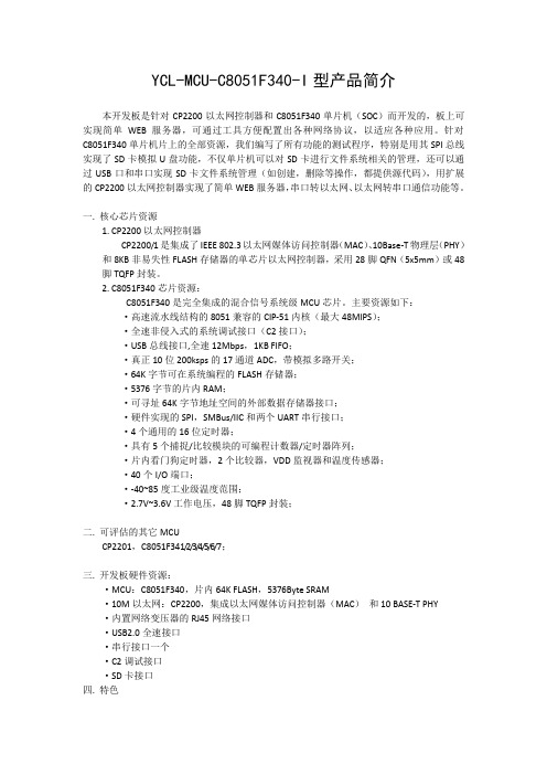
YCL-MCU-C8051F340-I型产品简介本开发板是针对CP2200以太网控制器和C8051F340单片机(SOC)而开发的,板上可实现简单WEB服务器,可通过工具方便配置出各种网络协议,以适应各种应用。
针对C8051F340单片机片上的全部资源,我们编写了所有功能的测试程序,特别是用其SPI总线实现了SD卡模拟U盘功能,不仅单片机可以对SD卡进行文件系统相关的管理,还可以通过USB口和串口实现SD卡文件系统管理(如创建,删除等操作,都提供源代码),用扩展的CP2200以太网控制器实现了简单WEB服务器,串口转以太网、以太网转串口通信功能等。
一. 核心芯片资源1. CP2200以太网控制器CP2200/1是集成了IEEE 802.3以太网媒体访问控制器(MAC)、10Base-T物理层(PHY)和8KB非易失性FLASH存储器的单芯片以太网控制器,采用28脚QFN(5x5mm)或48脚TQFP封装。
2. C8051F340芯片资源:C8051F340是完全集成的混合信号系统级MCU芯片。
主要资源如下:·高速流水线结构的8051兼容的CIP-51内核(最大48MIPS);·全速非侵入式的系统调试接口(C2接口);·USB总线接口,全速12Mbps,1KB FIFO;·真正10位200ksps的17通道ADC,带模拟多路开关;·64K字节可在系统编程的FLASH存储器;·5376字节的片内RAM;·可寻址64K字节地址空间的外部数据存储器接口;·硬件实现的SPI,SMBus/IIC和两个UART串行接口;·4个通用的16位定时器;·具有5个捕捉/比较模块的可编程计数器/定时器阵列;·片内看门狗定时器,2个比较器,VDD监视器和温度传感器;·40个I/O端口;·-40~85度工业级温度范围;·2.7V~3.6V工作电压,48脚TQFP封装;二. 可评估的其它MCUCP2201,C8051F341/2/3/4/5/6/7;三. 开发板硬件资源:·MCU:C8051F340,片内64K FLASH,5376Byte SRAM·10M以太网:CP2200,集成以太网媒体访问控制器(MAC)和10 BASE-T PHY·内置网络变压器的RJ45网络接口·USB2.0全速接口·串行接口一个·C2调试接口·SD卡接口四. 特色1. 支持通过USB口下载应用软件(更新固件),并提供全套源代码;2. 提供ARP,IP,ICMP,TCP协议的源代码,ARP中实现了缓存的学习、更新、老化、轮转替换。
(word完整版)1 C8051F单片机讲义
1 C8051F340单片机的并行接口一、综述GPIO,通用输入输出接口,是单片机与外部世界交换信息一种最简单的、最便洁、速度较快的一种接口方式,是其它接口方式的基础。
一个单片机的GPIO的数量,反映了这款单片机与外部世界交换信息的能力的大小。
有些单片机的GPIO只有几个,有些可达数十甚至数百个。
C8051F340单片机的GPIO,共有P0、P1、P2、P3、P4五组并行口,每组8个引脚,共占用40个引脚,分别称P0.0、P0。
1、P0。
2、P0。
3、P0.4、P0。
5、P0.6、P0。
7、P1.0……….P4.6、P4.7。
每一个引脚都可以做为输入口,也可以做为输出口。
如果做为输入口,有两种输入模式,分别是数字输入和模拟输入两种模式,如果做为输出口,也有两种输出模式,分别叫推挽输出、漏开输出。
C8051F340单片机,除了以上40个GPIO外,还有电源、调试、复位等8个引脚,合起来共同48个引脚.C8051F340单片机,是48脚的TQFP-48封装,表面贴的,与AT89S51/52、STC89C51/52比,管脚多,但占用的面积要小许多。
二、工作模式数字输入模式,是用来输入开关、按键等具有两个状态的量,只有0V、3。
3V两种合理的输入电压。
当然,稍有点误差,不会引起错误的读入结果。
模拟输入模式,是用来输入诸如表示电压、温度、压力等连续变化的量.输入电压的范围须在0~3。
3V之间,超出这个范围,可能引起芯片永久损坏.这部分内容将在以后的有关章节中介绍。
输出模式,也有两种,分别叫推挽输出、漏开输出。
推挽输出,是用两个MOS管,组成推挽电路,可以输出一个明确的电平.漏开输出,只用一个MOS管的漏极做输出,如果我们在漏极上用一个电阻,接上我们所需的电压,可以实现电压的灵活输出。
三、模式配置3.1 交叉开关如果使用C8051F340单片机的并行口,必须对寄存器XBR1的第六位置“1”,寄存器XBR1,叫交叉开关寄存器1,该寄存器的第六位,称XBARE,为交叉开关使能位。
基于C8051F340的Flash读写设计

西南科技大学专业方向设计报告西南科技大学信息工程学院制方向设计任务书方向设计学生日志方向设计评语表基于C8051F340的FLASH读写设计摘要:在电子技术研究和应用中,单片机始终是一个核心部件,单片机的应用也越来越广泛。
C8051F单片机是Silicon Labs 公司研发的一系列增强型51 单片机,广泛用于工业及民用电子、消费电子。
它继承了经典的传统51 的所有精华并在此基础上有重大发展。
W25X80FLASH存储器具有“PCB板占用空间少”、“引脚数量少”、“功耗低“等特点。
与普通串行FLASH相比,使用更灵活、性能更出色。
本设计要求使用C语言完成编程设计,并实现FLASH数据回读,且要求通过串口调试助手显示。
设计通过编程分步完成功能,最终达到设计要求。
详细设计步骤如下:系统时钟配置、端口配置、SPI通讯的初始化、初始化UART波特率、FLASH存储的初始化FLASH的擦除、FLASH写、从FLASH中读一个数组的数据。
完成程序设计后经过调试,实验结果表明该设计能够实现FLASH的读写并通过串口助手成功显示。
关键词:C8051F340;SPI;UART;FLASHAbstract: In the electronic technology research and application, single chip microcontroller is always a core components, the application of single chip microcontroller is also more and more widely. C8051F single chip microcontroller is a series of enhanced 51 single chip microcontroller which is researched by Silicon Labs company, it used widely in industry and civil electronics, consumer electronics. It inherits all essence from the classic tradition of 51 single chip microcontroller and has great development on this basis. The distinguishing feature of W25X80FLASH memory is "PCB board takes up less space", "pin the quantity is less", and "low power consumption" etc. Compared with ordinary serial FLASH, it uses more neatly and has more outstanding performance. This design needs C language, achieve the Flash data back to read, and display through the serial debugging assistant. Design is completed through the programming step by step, and finally reach the design requirements. The detailed design procedure is as follows: System clock configuration, port configuration, SPI communication initialization, initialization UART baud rate, Flash memory initialization, wipe out the FLASH, write on the Flash, read an array of data from the Flash. Complete the program design and put it through a test, the experimental results show that this design can realize FLASH literacy and show successful through the CommAssistant.Key W ords: C8051F340; SPI; UART; FLASH一、设计目的和意义FLASH存储器又称闪存,应为其具有快速读写,可编程擦除等性能在电子领域中被广泛使用。
C8051F340DK使用手册v0.9
C8051F340DK单片机开发板使用手册版本:V0.9C8051F网络完成日期:2009-3-23目录第一章.C8051F340DK开发板功能简介・・・・・・・・・・・・3第二章.C8051F340DK硬件接口详细说明・・・・・・・・・・・5第三章.C8051F340DK软件例程详细说明・・・・・・・・・・・8第四章.开发工具及开发软件KeilC安装配置・・・・・・・・・10 第五章.C8051F340DK常见问题・・・・・・・・・・・・・・・15 附录A:特别声明・・・・・・・・・・・・・・・・・・・・・15附录B:版本修定・・・・・・・・・・・・・・・・・・・・・15第一章.C8051F340DK开发板功能简介1.概述C8051F340DK是为技术研发人员和单片机爱好者开发的一款单片机开发板。
本开发板采用美国Silabs公司的C8051F340作为核心控制器,在搭配该公司的CP2200以太网控制芯片可完成工业以太网产品开发。
我们针对C8051F340单片机片上的全部资源,编写了所有功能的测试程序,对该单片机的性能做了全面的测试评估,使用方便。
使用该开发板能使开发者迅速掌握CP2200以太网控制器和C8051F340单片机的软硬件设计,大大缩短了产品开发周期。
2. C8051F340单片机主要特性(1)高速流水线结构的8051兼容的CIP-51内核,最高48MIPS执行速度;(2)全速非侵入式的系统调试接口(片内,C2接口);(3)真正10位200ksps的多通道单端/差分ADC,带模拟多路器;(4)高精度可编程的12MHz内部震荡器;(5)64KB字节可在系统编程的FLASH存储器;(6)4352(4096+256)字节的片内RAM;(7)USB 2.0通信接口,支持全速12Mbps通信和低速1.5Mbps通信(8)硬件实现的SPI,SMBus/IIC和2个UART串行接口;(9)4个通用的16位定时器;(10)具有5个捕捉/比较模块的可编程计数器/定时器阵列;(11)片内上电复位,看门狗定时器,2个电压比较器,VDD监视器和温度传感器;(12)40个I/O端口;(13)-40~85度工业级温度范围;(14)2.7V~3.6V工作电压,TQFP48封装;3.板上资源(1)MCU为美国Silabs公司C8051F340,64KB FLASH、(4096+256)B RAM、最高48MIPS执行速度;(2)外扩32KB SRAM(选用IS62LV256,速度70ns),外扩64KB串行FLASH (选用AT25F512,,也可以选用更大的FLASH);(3)2路10位AD输入,AIN1到AIN2输入信号量程0~+24.4V;(4)2路标准RS232通讯接口;(5)IIC接口的EEPROM AT24C02(可选更大容量的EEPROM);(6)IIC接口的RTC时钟,选用PCF8563, 带停电保护功能;(7)4*1 轻触键盘,蜂鸣器,LED指示;(8)JTAG(C2)调试接口;(9)两个LCD接口,支持多种厂家LCD,最高支持320×240;(10)USB从机通信;(11)10M以太网通讯接口,选用CP2200以太网通讯专用控制芯片;(12)外接P0/P1/P2/P3/P4 5个8位IO接口;(13)外扩总线接口;(14)C8051F340上的所有资源对用户开放;(15)USB供电;4.开发板软件例程(1)Delay: 软件延时程序,利用软件进行延时操作;(2)Key IO: 键盘读取及 IO信号输出控制程序;(3)EEPROM: IIC接口EEPROM(AT24C02A, 容量256字节)读写程序;(4)RTC: IIC接口实时时钟(PCF8563)读写程序;(5)RS232: 2路RS232串行数据通信程序;(6)ADC: 2路10 位AD采集示例程序;(7)LCD:1602字符型LCD显示驱动软件;(8)Timer: Timer0、Timer2、Timer3计时程序;(9)FLASH:外扩SPI串行Flash(AT25F512)擦除读写软件;(10)USB: USB通信示例程序;(11)WEB: TCP/IP协议栈及其应用通信程序;5.开发板配置:(1) C8051F340DK开发板1块;(2) 交叉串口线1条;(3) 交叉网线1条;(4) USB(电源)线1条;(5) 资料光盘1张;光盘内容:1) C8051F340DK使用手册;2)C8051F340DK原理图(PDF文件);3)实验程序源码(C语言);4)C8051F340DK主要元器件资料;5)KEIL C51 V8.02开发软件(2K代码限制);6)其它相关资料;6.开发板图片:第二章.C8051F340DK硬件接口说明1. ML-F020DK+硬件地址分配表接口或器件标识分配的地址说明IS62LV256 U6 0x0000-0x7FFF 外部扩展RAM地址CP2200 U9 0x8000-0x80FF 以太网芯片地址LCD1接口 JP10 0x9000-0x900F LCD1操作地址,接1602字符型液晶LCD2接口 JP11 0x8800-0x8803 LCD2操作地址, 支持T6963和SED1335控制芯片外扩总线 JP1 0xB800-0xBFFF 外部设备地址2.开发板接口列表标号功能说明连接对象JP1 外部总线扩展接口用户自定义JP2/3/4/5 C8051F340外接引脚用户自定义JP6 模拟信号输入接口(输入量程0~24.4V)外部设备(电压信号)JP7 RS232-2通信接口 RS232通信设备JP8 RS232-1通信接口 RS232通信设备JP10 液晶显示(LCD1)的接口接1602字符型液晶JP11 液晶显示(LCD2)的接口接以T6963和SED1335为控制芯片的各种型号液晶JP12 USB从机接口(也是电源接口)接PC机等USB主机设备外部USB供电,+5V JP13 JTAG接口,调试下载程序 C8051网络EC3仿真器JP14 10M以太网接口以太网设备3.JP1 总线扩展接口1 3 5 7 9 11 13 15 17 19 21 23 25A0 A2 A4 A6 A8 A10 nWR D0 D2 D4 D6 +3.3V+5V2 4 6 8 10 12 14 16 18 20 22 24 26A1 A3 A5 A7 A9 nRD nEX_CS D1 D3 D5 D7 GND GND说明:(1)地址总线(A0-A10)、数据总线(D0-D7)和控制总线(nRD 、nWR、nEX_CS)电平为3.3V;(2)地址范围:0xB800-0xBFFF;4. JP2、JP3、JP4、JP5为C8051F340单片机所有管脚引出接口,可由客户自由使用,但要注意在板子的原有电路的影响。
单片机开发板设计
引言概述:单片机开发板是用于学习和开发嵌入式系统的重要工具。
本文将进一步深入探讨单片机开发板设计的相关内容,包括选择合适的单片机型号、电路设计、外设接口设计、调试与测试、以及最后的PCB设计和制造。
通过本文的阐述,读者将了解到单片机开发板设计的基本原理和步骤,并能够在实际项目中应用这些知识。
正文内容:一、选择合适的单片机型号1.根据应用需求选择单片机型号,考虑处理器性能、存储容量、功耗等因素。
2.了解单片机供应商的技术支持和开发工具,以便后续开发和调试。
3.考虑扩展性和可编程性,选择具备足够IO口和外部总线接口的单片机。
二、电路设计1.确定系统的电源需求,并设计稳定可靠的电源电路。
2.设计复位电路,保证单片机正确启动和初始化。
3.制定时钟源电路的设计,保证单片机正常工作的时钟信号。
4.设计复杂外设电路,如LCD显示器、键盘等。
5.考虑电路抗干扰性,采取相应的措施来减少电磁干扰和噪声。
三、外设接口设计1.根据需求添加适当的外设接口,如UART、SPI、I2C、PWM 等。
2.考虑外设接口的连接方式和电路保护措施。
3.设计通信接口电路,如USB、以太网等。
4.添加扩展接口,用于外部模块的连接和扩展。
5.采用标准化接口和协议,确保兼容性和可替换性。
四、调试与测试1.搭建调试环境,包括硬件调试工具和软件开发工具。
2.编写测试代码,进行单片机和外设的功能验证。
3.使用示波器和逻辑分析仪等工具进行信号调试和波形分析。
4.添加调试接口,如JTAG、SWD等,方便后续调试和故障排查。
5.进行系统整体测试和性能优化,确保系统的稳定性和可靠性。
五、PCB设计和制造1.进行原理图设计,根据电路布局和电源需求绘制电路图。
2.完成PCB布局设计,考虑进行分层布线和信号的最佳走线。
3.进行信号完整性分析,考虑电磁干扰和信号串扰等问题。
4.自动PCB制造文件,包括Gerber文件和钻孔文件等。
5.选择合适的PCB厂商进行制造,注意质量控制和交付时间。
基于C8051F340单片机的移动机器人避障系统设计

第20卷第12期长春大学学报Vol.20No.12 2010年12月JOURNAL OF CHANGCHUN UNIVERSITY Dec.2010基于C8051F340单片机的移动机器人避障系统设计赵银银(北华大学工程训练中心,吉林吉林132021)摘要:介绍了一种基于C8051F340单片机的移动机器人超声波测距避障系统,阐述了系统结构、工作原理、设计方法,实验结果表明该系统具有硬件结构简单、高精度、微型化等特点。
关键词:移动机器人;超声传感器;C8051F340单片机中图分类号:TP24文献标志码:A文章编号:1009-3907(2010)12-0021-03移动机器人研究的一个基本问题是安全避障,实现安全避障的前提是准确获取避障信息,准确的避障信息为移动机器人的避障[1]处理提供了可靠的周边环境信息。
对于测距和障碍探测,采用最多的是红外线和超声波传感器。
超声波测距由于其成本低廉,是一种常见的测距方法,但由于超声波传感器具有探测波束角过大、方向性差、等缺点,而采用多传感器又会占用控制器很多资源,且传感器间存在交叉干扰,往往不能对障碍物进行准确定位。
本文介绍一种以C8051F340单片机为核心的高精度、微型化的多传感器测距系统,实现移动机器人的安全避障。
1超声波测距原理超声测距从原理上可分为共振式、脉冲反射式两种。
由于共振法的应用要求复杂,这里使用脉冲反射式。
测距的基本原理[2]是发送(超声)压力波包,并测量该波包发射和回到接收器所占用的时间,即L=CT/ 2,其中L为目标距超声波传感器的距离,C为超声速度,T为发射到接收的时间间隔。
由于声速C与温度有关,为了提高测量精度,应通过温度补偿的方法对声速加以校正。
如表1为声速与温度关系表。
表1声速与温度关系表温度ħ-30-20-100102030100声速m/s3133193253233383443493862系统硬件设计本系统采用5组超声传波传感器,分别于机器人的左方、偏左方、前方、偏右方、右方各安装一组超声波传感器,相互间隔45度角,用于探测各自方向上障碍物的信息。
基于C8051F系列单片机的低功耗设计毕业设计(论文)
基于C8051F系列单片机的低功耗设计摘要着重介绍C805lF系列单片机功耗的计算方法及系统低功耗设计的策略.内容包括有关的内部和外部振荡器、CPU的电源管理模式、系统的时钟频率.工作电压对系统功耗的影响.以及如何合理地配置它们来降低功耗。
最后,给出有关数据采集系统的设计实例。
关建词C8051F单片机低功耗电源管理引言在控制终端系统设计中,当系统要求整体功耗偏低时,C8051F系列单片机是一个最佳的选择。
它们拥有灵活的时钟硬件,使系统能够方便地在高效运作模式与低功耗模式问进行转换,智能的电源管理模式能够在正常工作及待机状态自由切换,从而降低整个系统的能量损耗;当工作频率低于10kHz时,时钟丢失检测器(MCD)能够引发系统产生复位,确保系统工作的安全可靠。
1 C8051F各部分组件的功耗当一个系统对功耗要求严格时,可以在硬件电路建立前首先粗略计算一下整个系统所需的功耗。
由于C8051F系列单片机为数模混合SOC系统,能够实现整个设计的大部分功能,因此整个设计系统的功耗将主要集中在C805IF系列单片机的能量消耗上。
整个单片机系统的功耗应该由4部分组成:振荡器功耗、数字设备功耗、模拟外设功耗及I/O端口功耗。
振荡器功耗包括内部振荡器的功耗以及外部振荡器功耗。
数字设备能量消耗主要由CPU的工作模式、工作电压及系统时钟频率决定。
温度与数字外围设备对数字设备的功耗影响很小。
模拟外围设备功耗主要包含ADC、电压基准VREF、温度传感器、偏压发生器及内部振荡器。
比较器也有少量的能量损耗。
1.1 振荡器功耗分析外部振荡器具有很高的可配置性,为系统设计者提供了多种选择。
时基信号可以从外部CMOS电平时钟源、晶振或陶瓷谐振器、RC组合电路或外部电容获得,每一种方法都有各自的优势。
由于振荡器可以灵巧地在各种方式中转换,因此可以通过改变振荡器来降低功耗。
对外部振荡器来说,外部CMOS时钟、电容和RC网络都能够提供较低的振荡频率。
C8051F31 X 开发板用户指南说明书
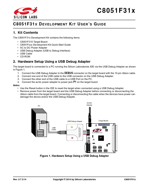
Rev. 0.7 2/14Copyright © 2014 by Silicon LaboratoriesC8051F31xX EVELOPMENT IT SER S UIDE1. Kit ContentsThe C8051F31x Development Kit contains the following items:•C8051F310 Target Board•C8051Fxxx Development Kit Quick-Start Guide •AC to DC Power Adapter•USB Debug Adapter (USB to Debug Interface)•USB Cable •CD-ROM2. Hardware Setup Using a USB Debug AdapterThe target board is connected to a PC running the Silicon Laboratories IDE via the USB Debug Adapter as shown in Figure 1.1.Connect the USB Debug Adapter to the DEBUG connector on the target board with the 10-pin ribbon cable.2.Connect one end of the USB cable to the USB connector on the USB Debug Adapter.3.Connect the other end of the USB cable to a USB Port on the PC.4.Connect the ac/dc power adapter to power jack P1 on the target board.Notes:•Use the Reset button in the IDE to reset the target when connected using a USB Debug Adapter.•Remove power from the target board and the USB Debug Adapter before connecting or disconnecting the ribbon cable from the target board. Connecting or disconnecting the cable when the devices have power can damage the device and/or the USB Debug Adapter.Figure 1.Hardware Setup Using a USB Debug AdapterPWRP1.6C8051F31x3. Software SetupSimplicity Studio greatly reduces development time and complexity with Silicon Labs EFM32 and 8051 MCU products by providing a high-powered IDE, tools for hardware configuration, and links to helpful resources, all in one place.Once Simplicity Studio is installed, the application itself can be used to install additional software and documentation components to aid in the development and evaluation process.Figure2.Simplicity StudioThe following Simplicity Studio components are required for the C8051F310 Development Kit:⏹ 8051 Products Part Support ⏹ Simplicity Developer PlatformDownload and install Simplicity Studio from /8bit-software or /simplicity-studio .Once installed, run Simplicity Studio by selecting Start →Silicon Labs →Simplicity Studio →Simplicity Studio from the start menu or clicking the Simplicity Studio shortcut on the desktop. Follow the instructions to install the software and click Simplicity IDE to launch the IDE.The first time the project creation wizard runs, the Setup Environment wizard will guide the user through the process of configuring the build tools and SDK selection.In the Part Selection step of the wizard, select from the list of installed parts only the parts to use during development. Choosing parts and families in this step affects the displayed or filtered parts in the later device selection menus. Choose the C8051F31x family by checking the C8051F31x check box. Modify the part selection at any time by accessing the Part Management dialog from the Window →Preferences →Simplicity Studio →Part Management menu item.Simplicity Studio can detect if certain toolchains are not activated. If the Licensing Helper is displayed after completing the Setup Environment wizard, follow the instructions to activate the toolchain.C8051F31x3.1. Running BlinkyEach project has its own source files, target configuration, SDK configuration, and build configurations such as the Debug and Release build configurations. The IDE can be used to manage multiple projects in a collection called a workspace. Workspace settings are applied globally to all projects within the workspace. This can include settings such as key bindings, window preferences, and code style and formatting options. Project actions, such as build and debug are context sensitive. For example, the user must select a project in the Project Explorer view in order to build that project.To create a project based on the Blinky example:1. Click the Simplicity IDE tile from the Simplicity Studio home screen.2. Click the Create new project link from the welcome screen or go to File →New →Silicon Labs MCU Project .3. In the Kit drop-down, select C8051F310 Development Kit , in the Part drop-down, select C8051F310, and in the SDK drop-down, select the desired SDK. Click Next .4. Select Example and click Next .5. Under C8051F310 Development Kit in the Blinky folder, select F31x Blinky and click Finish .6. Click on the project in the Project Explorer and click Build , the hammer icon in the top bar. Alternatively, go to Project →Build Project .7. Click Debug to download the project to the hardware and start a debug session.8. Press the Resumebutton to start the code running. The LED should blink.9. Press the Suspend button to stop the code.10. Press the Reset the devicebutton to reset the target MCU.11. Press the Disconnectbutton to return to the development perspective.3.2. Simplicity Studio HelpSimplicity Studio includes detailed help information and device documentation within the tool. The help containsdescriptions for each dialog window. To view the documentation for a dialog, click the question mark icon in the window:This will open a pane specific to the dialog with additional details.The documentation within the tool can also be viewed by going to Help →Help Contents or Help →Search .C8051F31x3.3. Legacy 8-bit IDENote:Using the Simplicity Studio tools with the C8051F310 Development Kit is recommended. See section 3. "SoftwareSetup‚" on page 2 for more information.Download the 8-bit software from the website (/8bit-software ) or use the provided installer on the CD-ROM to install the software tools for the C8051F31x devices. After installation, examples can be found in ...\Examples\C8051F31x in the installation directory. At a minimum, the C8051F310 DK requires:⏹ Silicon Labs IDE —Software enabling initial evaluation, development, and debugging.⏹ Configuration Wizard 2—Initialization code generation software for the C8051F31x devices.⏹ Keil C51 Tools —Keil 8051 Compiler/Assembler/Linker toolchain.Other software available includes:⏹ Keil µVision Driver —Driver for the Keil µVision IDE that enables development and debugging onC8051Fxxx MCUs.⏹ Flash Programming Utilities and MCU Production Programmer —Programming utilities for the production line. More information on the available programming options can be found on the website:/products/mcu/Pages/ProgrammingOptions.aspx .⏹ ToolStick Development Tools —Software and examples for the ToolStick development platform. More information on this platform can be found at /toolstick .The development kit includes the latest version of the C51 Keil 8051 toolset. This toolset is initially limited to a code size of 2kB and programs start at code address 0x0800. After registration, the code size limit is removed entirely and programs will start at code address 0x0000.To register the Keil toolset:1. Find the Product Serial Number printed on the CD-ROM. If you no longer have this serial number, register on the Silicon Labs website (/8bit-software ) to obtain the serial number.2. Open the Keil µVision4 IDE from the installation directory with administrative privileges.3. Select FileLicense Management to open the License Management window.Figure 3.Keil µVision4 IDE License Management Window4. Click on the Get LIC via Internet... button to open the Obtaining a License IDE Code (LIC) window.5. Press OK to open a browser window to the Keil website. If the window doesn’t open, navigate to /license/install.htm .6. Enter the Silicon Labs Product Serial Number printed on the CD-ROM, along with any additional requiredC8051F31xinformation.7. Once the form is complete, click the Submit button. An email will be sent to the provided email addresswith the license activation code.8. Copy the License ID Code (LIC) from the email.9. Paste the LIC into the New License ID Code (LIC) text box at the bottom of the License Managementwindow in µVision4.10. Press the Add LIC button. The window should now list the PK51 Prof. Developers Kit for Silabs as alicensed product.11. Click the Close button.C8051F31x4. Target BoardThe C8051F31x Development Kit includes a target board with a C8051F310 device pre-installed for evaluation and preliminary software development. Numerous input/output (I/O) connections are provided to facilitate prototyping using the target board. Refer to Figure4 for the locations of the various I/O connectors.P1Power connector (accepts input from 7 to 15 VDC unregulated power adapter)J134-pin Expansion I/O connectorJ3Port I/O Configuration connectorJ4DEBUG connector for Debug Adapter interfaceJ5DB-9 connector for UART0 RS232 interfaceJ6Analog I/O terminal blockJ7Low pass filter connectorJ8USB Debug Adapter target board power connectorJ9, J10External crystal enable connectorsFigure4.C8051F310 Target BoardC8051F31x4.1. System Clock SourcesThe C8051F310 device installed on the target board features a calibrated programmable internal oscillator which is enabled as the system clock source on reset. After reset, the internal oscillator operates at a frequency of 3.0625MHz (±2%) by default but may be configured by software to operate at other frequencies. Therefore, in many applications an external oscillator is not required. However, if you wish to operate the C8051F310 device at a fre-quency not available with the internal oscillator, an external crystal may be used. Refer to the C8051F31x data sheet for more information on configuring the system clock source.The target board is designed to facilitate the installation of an external crystal. Remove shorting blocks at headers J9 and J10 and install the crystal at the pads marked Y1. Install a 10M resistor at R9 and install capacitors at C14 and C15 using values appropriate for the crystal you select. Refer to the C8051F31x data sheet for more infor-mation on the use of external oscillators.4.2. Switches and LEDsTwo switches are provided on the target board. Switch SW1 is connected to the RESET pin of the C8051F310. Pressing SW1 puts the device into its hardware-reset state. Switch SW2 is connected to the C8051F310’s general purpose I/O (GPIO) pin through headers. Pressing SW2 generates a logic low signal on the port pin. Remove the shorting block from the header to disconnect SW2 from the port pins. The port pin signal is also routed to a pin on the J1 I/O connector. See Table1 for the port pins and headers corresponding to each switch.Two LEDs are also provided on the target board. The red LED labeled PWR is used to indicate a power connection to the target board. The green LED labeled with a port pin name is connected to the C8051F310’s GPIO pin through headers. Remove the shorting block from the header to disconnect the LED from the port pin. The port pin signal is also routed to a pin on the J1 I/O connector. See Table1 for the port pins and headers corresponding to each LED.Table 1. Target Board I/O DescriptionsDescription I/O HeaderSW1Reset noneSW2P0.7J3[3-4]Green LED P3.3J3[1-2]Red LED PWR noneC8051F31x4.3. Expansion I/O Connector (J1)The 34-pin Expansion I/O connector J1 provides access to all signal pins of the C8051F310 device. Pins for +3V, digital ground and the output of an on-board low-pass filter are also available. A small through-hole prototyping area is also provided. All I/O signals routed to connector J1 are also routed to through-hole connection points between J1 and the prototyping area (see Figure4 on page6). Each connection point is labeled indicating the signal available at the connection point. See Table2 for a list of pin descriptions for J1.Table 2. J1 Pin DescriptionsPin #Description Pin #Description Pin #Description1+3VD(+3.3VDC)13P1.225P2.62PWM Output14P1.326P2.73P0.015P1.427P3.04P0.116P1.528P3.15P0.217P1.629P3.26P0.318P1.730P3.37P0.419P2.031P3.48P0.520P2.132/RST (Reset)9P0.621P2.233GND (Ground)10P0.722P2.334GND (Ground)11P1.023P2.412P1.124P2.54.4. Target Board DEBUG Interface (J4)The DEBUG connector (J4) provides access to the DEBUG (C2) pins of the C8051F310. It is used to connect the Serial Adapter or the USB Debug Adapter to the target board for in-circuit debugging and Flash programming. Table3 shows the DEBUG pin definitions.Table 3. DEBUG Connector Pin DescriptionsPin #Description1+3VD(+3.3VDC)2, 3, 9GND (Ground)4C2D5/RST(Reset)6P3.07C2CK8Not Connected10USB PowerC8051F31x4.5. Serial Interface (J5)A RS232 transceiver circuit and DB-9 (J5) connector are provided on the target board to facilitate serial connec-tions to UART0 of the C8051F310. The TX, RX, RTS and CTS signals of UART0 may be connected to the DB-9 connector and transceiver by installing shorting blocks on header J3.J3[5–6]- Install shorting block to connect UART0 TX (P0.4) to transceiver.J3[7–8]- Install shorting block to connect UART0 RX (P0.5) to transceiver.J3[9–10]- Install shorting block to connect UART0 RTS (P3.1) to transceiver.J3[11–12]- Install shorting block to connect UART0 CTS (P3.2) to transceiver.4.6. Analog I/O (J6)Several of the C8051F310 target device’s port pins are connected to the J6 terminal block. Refer to Table4 for the J6 terminal block connections. Install a shorting block on J7[2-3] to connect the AIN2.4 input to the P2.4 pin of the target device.Table 4. J6 Terminal Block Pin DescriptionsPin #Description1P2.5 / AIN2.52AIN2.43GND (Ground)4P0.0 / Vref (Voltage Reference)4.7. USB Debug Adapter Target Board Power Connector (J8)The USB Debug Adapter includes a connection to provide power to the target board. This connection is routed from J4[10] to J8[1]. Place a shorting block at header J8[2–3] to power the board directly from an ac/dc power adapter. Place a shorting block at header J8[1–2] to power the board from the USB Debug Adapter. Please note that the second option is not supported with either the EC1 or EC2 Serial Adapters.4.8. Low-Pass Filter (J7)The C8051F310 target board features a low-pass filter that may be connected to port pin P2.4. Install a shorting block on J7[1–2] to connect the P2.4 pin of the target device to the low-pass filter input. The output of the low-pass filter is routed to the PWM signal at J1[2]. The C8051F310 may be programmed to generate a PWM (Pulse-Width Modulated) waveform which is then input to the low-pass filter to implement a user-controlled PWM digital-to-ana-log converter. Refer to Applications Note “AN107: Implementing 16-Bit PWM Using the PCA” in the “documenta-tion” directory on the CD-ROM for a discussion on generating a programmable dc voltage level with a PWM waveform and low-pass filter.C8051F31xC8051F31x D OCUMENT C HANGE L ISTRevision 0.4 to Revision 0.5⏹ Section 1, added USB Debug Adapter and USB Cable.⏹ Section 2, changed name from "Hardware Setup" to "Hardware Setup using an EC2 Serial Adapter".⏹ Section 2, added 2 Notes bullets.⏹ Section 2, removed Note from bottom of page.⏹ Added Section 3, "Hardware Setup using a USB Debug Adapter".⏹ Section 5.4.2, changed step 2 to include new instructions.⏹ Section 7, J4, changed "Serial Adapter" to "Debug Adapter".⏹ Target Board DEBUG Interface Section, added USB Debug Adapter.⏹ DEBUG Connector Pin Descriptions Table, changed pin 4 to C2D.⏹ Changed "jumper" to "header".⏹ EC2 Serial Adapter section, added EC2 to the section title, table title and figure title.⏹ EC2 Serial Adapter section, changed "JTAG" to "DEBUG".⏹ Added "USB Debug Adapter" section.⏹ Section 7, J8, changed "Serial Adapter" to "USB Debug Adapter".⏹ DEBUG Connector Pin Descriptions Table, changed pin 10 to USB Power.⏹ USB Debug Adapter Target Board Power Connector (J8) Section, changed "Serial" to "USB Debug". Revision 0.5 to Revision 0.6⏹ Removed EC2 Serial Adapter from Kit Contents.⏹ Removed Section 2. Hardware Setup using an EC2 Serial Adapter. See RS232 Serial Adapter (EC2)User's Guide.⏹ Removed Section 8. EC2 Serial Adapter. See RS232 Serial Adapter (EC2) User's Guide.⏹ Removed Section 9. USB Debug Adapter. See USB Debug Adapter User's Guide.Revision 0.6 to Revision 0.7⏹ Updated 3. "Software Setup‚" on page 2.DisclaimerSilicon Laboratories intends to provide customers with the latest, accurate, and in-depth documentation of all peripherals and modules available for system and software implementers using or intending to use the Silicon Laboratories products. Characterization data, available modules and peripherals, memory sizes and memory addresses refer to each specific device, and "Typical" parameters provided can and do vary in different applications. Application examples described herein are for illustrative purposes only. Silicon Laboratories reserves the right to make changes without further notice and limitation to product information, specifications, and descriptions herein, and does not give warranties as to the accuracy or completeness of the included information. Silicon Laboratories shall have no liability for the consequences of use of the information supplied herein. This document does not imply or express copyright licenses granted hereunder to design or fabricate any integrated circuits. The products must not be used within any Life Support System without the specific written consent of Silicon Laboratories. A "Life Support System" is any product or system intended to support or sustain life and/or health, which, if it fails, can be reasonably expected to result in significant personal injury or death. Silicon Laboratories products are generally not intended for military applications. Silicon Laboratories products shall under no circumstances be used in weapons of mass destruction including (but not limited to) nuclear, biological or chemical weapons, or missiles capable of delivering such weapons.Trademark InformationSilicon Laboratories Inc., Silicon Laboratories, Silicon Labs, SiLabs and the Silicon Labs logo, CMEMS®, EFM, EFM32, EFR, Energy Micro, Energy Micro logo and combinations thereof, "the world’s most energy friendly microcontrollers", Ember®, EZLink®, EZMac®, EZRadio®, EZRadioPRO®, DSPLL®, ISOmodem ®, Precision32®, ProSLIC®, SiPHY®, USBXpress® and others are trademarks or registered trademarks of Silicon Laboratories Inc. ARM, CORTEX, Cortex-M3 and THUMB are trademarks or registered trademarks of ARM Holdings. Keil is a registered trademark of ARM Limited. All other products or brand names mentioned herein are trademarks of their respective holders. Silicon Laboratories Inc.400 West Cesar ChavezAustin, TX 78701USAIoT Portfolio/IoT SW/HW /simplicity Quality /quality Support and Community 。
C8051F单片机实验系统设计

C8051F单片机实验系统设计摘要:为满足单片机学习中对实践技能的要求,提高单片机开发系统的稳定性和可扩展性,降低系统功耗,设计了一种基于FPGA的C8051F单片机开发板。
利用FPGA实现键盘扫描、液晶驱动、地址译码以及其他外设接口,大幅度简化外围电路结构。
系统可在高低频时钟间切换以减小功耗,并增加了音频处理模块,实现基本的音频信号的存储和回放。
实验结果表明,该电路板相比普通的单片机开发板系统功耗减小50%左右,拥有最高达25 MIPS的处理速度,单片机可以直接驱动多达20多个LS TTL门电路,FPGA的引入使得外扩其他电路更为方便和灵活,具有良好的扩展性。
关键词:单片机;FPGA;外围电路;电路板目前高校单片机教学中大多是以MCS51单片机为首选机型进行讲解,所开发的教学实验系统也多是基于MCS51系列单片机开发设计的。
然而,随着单片机的应用进入SoC时代,其不足和缺陷也显而易见:片上资源不够丰富,功耗较大,处理速度很有限,电路庞大且复杂,可靠性和可维护性较差,难以满足高水平的设计要求。
为了进一步简化电路结构,提出一种C8051F单片机实验系统设计方案,该方案采用FPGA实现单片机各种外设接口。
FPGA作为一种可编程逻辑器件凭借其优越的可扩展性能受到设计者的青睐,逐渐成为分立元件的替代者。
通过对FPGA编程,实现任何数字元件的逻辑功能,设计者可以通过原理图输入或硬件描述语言,方便地设计一个数字系统,这使得单片机外围电路的设计简单、灵活、可靠。
本系统是为单片机实践教学而开发的,因此要求单片机的功能齐全,满足教学中各种实验的要求。
一般的实验板的功能有:模拟数字信号转换实验、通信接口实验、存储器实验、各种显示实验,人机交互实验等等。
除此之外,还要考虑由于是非商业性质的开发,对一些功能的精度要求不是很高,在选择最理想价格的同时,选择尽可能多而全的片上资源,留待后期开发扩充。
基于以上考虑,该平台使用SoC系统级的C8051F020单片机作为核心控制器,CycloneⅡEP2C8型FPGA 实现外设接口,加上LCD、键盘、UART串口等人机交互的模块。
在KEIL4环境下开发C8051F系列的单片机
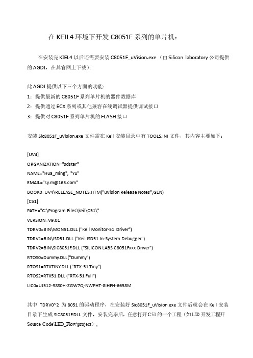
在KEIL4环境下开发C8051F系列的单片机:在安装完KIEL4以后还需要安装C8051F_uVision.exe(由Silicon laboratory公司提供的AGDI,在其官网上下载);此AGDI提供以下三个方面的功能:1:提供最新的C8051F系列单片机的器件数据库2:提供通过ECX系列或其他兼容在线调试器提供调试接口3:提供对C8051F系列单片机的FLASH接口安装Sic8051F_uVision.exe文件需在Keil安装目录中有TOOLS.INI文件,其内容主要如下:[UV4]ORGANIZATION="sdstar"NAME="Hua_ming", "Yu"EMAIL="sy.m@"BOOK0=UV4\RELEASE_NOTES.HTM("uVision Release Notes",GEN)[C51]PATH="C:\Program Files\keil\C51\"VERSION=V9.01TDRV0=BIN\MON51.DLL ("Keil Monitor-51 Driver")TDRV1=BIN\ISD51.DLL ("Keil ISD51 In-System Debugger")TDRV2=BIN\SIC8051F.DLL ("SILICON LABS C8051Fxxx Driver")RTOS0=Dummy.DLL("Dummy")RTOS1=RTXTINY.DLL ("RTX-51 Tiny")RTOS2=RTX51.DLL ("RTX-51 Full")LIC0=UJ512-98S0H-ZGW7Q-NWPHT-8IHFH-6658M其中TDRV0~2 为8051的驱动程序,在安装好Sic8051F_uVision.exe文件后就会在Keil安装目录下生成SIC8051F.DLL文件,安装完毕后,任意打开C51的一个工程(如LED开发工程开Source Code\LED_Flow\project),先进行一系列的设置。
C8051单片机实验指导书

51单片机实验开发板设计

东 北 石 油 大 学课 程 设 计2012年 7 月 8日 课 程 单片机课程设计 题 目 51单片机实验开发板设计 院 系 电气信息工程学院测控系专业班级测控09学生姓名 学生学号指导教师东北石油大学课程设计任务书课程单片机课程设计题目51单片机实验开发板设计专业测控技术与仪器姓名学号一、任务设计一款基于PROTEUS7.2仿真软件实现的51单片机实验开发板。
二、设计要求[1] 该实验开发板力求单片机IO口分配合理,实验板硬件资源丰富。
[2] 外围电路设计合理,程序例程正确。
[3] 基本电路包括:单片机最小系统、8位流水灯电路、LED显示电路、蜂鸣器电路、键盘电路、1602及12864液晶显示电路。
[4] 提交设计报告、电路图及程序源码。
三、参考资料[1] 潘永雄.新编单片机原理与应用[M].西安电子科技大学出版社,2003.[2] 丁元杰.单片微机原理与应用[M].机械工业出版社,2006.[3] 朱定华.单片微机原理及接口技术实验[M].北方交通大学出版社,2002.[4] 付家才.单片机控制工程实践技术[M].化学工业出版社,2004.[5] 杨丽凤,王艳秋,张军.单片机原理与接口技术[M].清华大学、北方交通大学出版社,2004.完成期限2012.6.29 至2012.7.8指导教师专业负责人曹广华2012年6月29 日目录第1章绪论 (2)1.1 单片机现状与发展 (2)1.2 单片机的性能特点 (2)1.3 本设计任务 (3)第2 章总体方案论证与设计 (4)2.1 电源 (4)2.2 显示功能方案 (4)2.3 电位指示选择 (4)2.4 总体硬件组成框图 (4)第3章系统硬件设计 (6)3.1 单片机最小系统 (6)3.2 键盘模块设计 (7)3.3 LED显示模块设计 (7)3.4 流水灯显示模块设计 (8)3.5 发声模块设计 (9)3.6 串口通信模块设计 (9)第4章系统的软件设计 (10)4.1 LED模块的程序设计 (10)4.2 键盘模块的软件设计 (11)第5章系统调试与测试结果分析 (12)5.1 使用的仪器仪表 (12)5.2 系统调试 (12)5.3 测试结果 (13)结论 (14)参考文献 (15)附录1 程序 (16)第1章绪论由于单片机技术在各个领域正得到越来越广泛的应用,许多集成电路生产厂家相继推出了各种类型的单片机,在单片机家族的众多成员中,MCS.51系列单片机以其优越的性能、成熟的技术及高可靠性和高性能价格比,迅速占领了市场,成为国内单片机应用领域中的主流。
C8051F340单片机对智能测量系统的控制设计
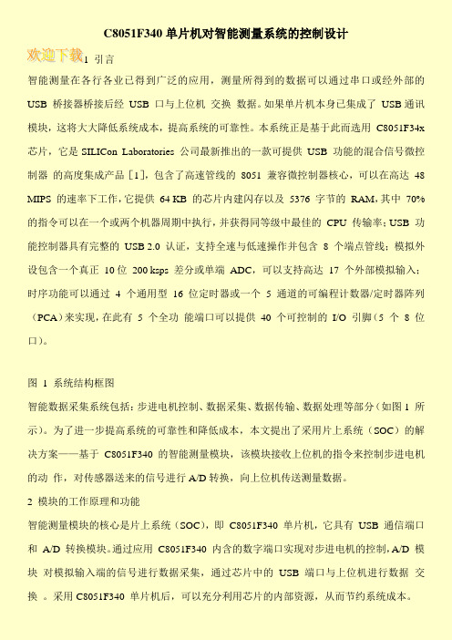
C8051F340单片机对智能测量系统的控制设计1 引言智能测量在各行各业已得到广泛的应用,测量所得到的数据可以通过串口或经外部的USB 桥接器桥接后经USB 口与上位机交换数据。
如果单片机本身已集成了USB通讯模块,这将大大降低系统成本,提高系统的可靠性。
本系统正是基于此而选用C8051F34x 芯片,它是SILICon Laboratories 公司最新推出的一款可提供USB 功能的混合信号微控制器的高度集成产品[1],包含了高速管线的8051 兼容微控制器核心,可以在高达48 MIPS 的速率下工作,它提供64 KB 的芯片内建闪存以及5376 字节的RAM,其中70%的指令可以在一个或两个机器周期中执行,并获得同等级中最佳的CPU 传输率;USB 功能控制器具有完整的USB 2.0 认证,支持全速与低速操作并包含8 个端点管线;模拟外设包含一个真正10位200 ksps 差分或单端ADC,可以支持高达17 个外部模拟输入;时序功能可以通过 4 个通用型16 位定时器或一个 5 通道的可编程计数器/定时器阵列(PCA)来实现,在此有5 个全功能端口可以提供40 个可控制的I/O 引脚(5 个8 位口)。
图1 系统结构框图智能数据采集系统包括:步进电机控制、数据采集、数据传输、数据处理等部分(如图1 所示)。
为了进一步提高系统的可靠性和降低成本,本文提出了采用片上系统(SOC)的解决方案——基于C8051F340 的智能测量模块,该模块接收上位机的指令来控制步进电机的动作,对传感器送来的信号进行A/D转换,向上位机传送测量数据。
2 模块的工作原理和功能智能测量模块的核心是片上系统(SOC),即C8051F340 单片机,它具有USB 通信端口和A/D 转换模块。
通过应用C8051F340 内含的数字端口实现对步进电机的控制,A/D 模块对模拟输入端的信号进行数据采集,通过芯片中的USB 端口与上位机进行数据交换。