电子科大2011数电期末考试题A卷-参考解答
电子科技大学期末数字电子技术考试题a卷-参考答案
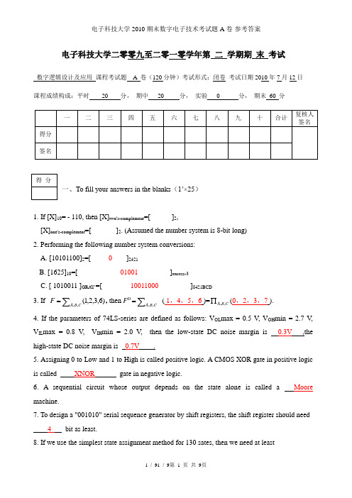
电子科技大学二零零九至二零一零学年第 二 学期期 末 考试数字逻辑设计及应用 课程考试题 A 卷(120分钟)考试形式:闭卷 考试日期2010年7月12日课程成绩构成:平时 20 分, 期中 20 分, 实验 0 分, 期末 60 分一、To fill your answers in the blanks (1’×25)1. If [X]10= - 110, then [X]two's-complement =[ ]2,[X]one's-complement =[ ]2. (Assumed the number system is 8-bit long) 2. Performing the following number system conversions: A. [10101100]2=[ 0 ]2421B. [1625]10=[01001 ]excess-3C. [ 1010011 ]GRAY =[10011000 ]8421BCD3. If ∑=C B A F ,,)6,3,2,1(, then F D ∑=C B A ,,( 1,4,5,6 )=C B A ,,∏(0,2,3,7 ).4. If the parameters of 74LS-series are defined as follows: V OL max = 0.5 V , V OH min = 2.7 V , V IL max = 0.8 V , V IH min = 2.0 V , then the low-state DC noise margin is 0.3V ,the high-state DC noise margin is 0.7V .5. Assigning 0 to Low and 1 to High is called positive logic. A CMOS XOR gate in positive logic is called XNOR gate in negative logic.6. A sequential circuit whose output depends on the state alone is called a Moore machine.7. To design a "001010" serial sequence generator by shift registers, the shift register should need 4 bit as least.8. If we use the simplest state assignment method for 130 sates, then we need at least8state variables.9. One state transition equation is Q*=JQ'+K'Q. If we use D flip-flop to complete the equation, the D input terminal of D flip-flop should be have the function D= JQ'+K'Q.10.Which state in Fig. 1 is ambiguous D11.A CMOS circuit is shown as Fig. 2, its logic function z= A’B’+ABFig. 1 Fig. 212.If number [A]two's-complement =01101010 and [B]one's-complement =1001, calculate [A-B]two's-complement and indicate whether or not overflow occurs.(Assumed the number system is 8-bit long)[A-B]two's-complement = 01110000, overflow no13. If a RAM’s capacity is 16K words × 8 bits, the address inputs should be 14bits; We need 8chips of 8K ⨯8 bits RAM to form a 16 K ⨯ 32 bits ROM..14. Which is the XOR gate of the following circuit A .15.There are 2n-n invalid states in an n-bit ring counter state diagram.16.An unused CMOS NOR input should be tied to logic Low level or 0 .17.The function of a DAC is translating the Digital inputs to the same value of analogoutputs.二、Complete the following truth table of taking a vote by A,B,C, when more than two of A,B,C approve a resolution, the resolution is passed; at the same time, the resolution can’t go through if A don’t agree.For A,B,C, assume 1 is indicated approval, 0 is indicated opposition. For the F,A B C F三、The circuit to the below realizes a combinational function F of four variables. Fill in the Karnaugh map of the logic function F realized by the multiplexer-based circuit. (6’)四、(A) Minimize the logic function expressionF = A·B + AC’ +B’·C+BC’+B’D+BD’+ADE(H+G) (5’)F = A·B + AC’ +B’·C+BC’+B’D+BD’ = A·(B ’C )’ +B’·C+BC’+B’D+BD’= A +B’·C+BC’+B’D+BD’+C ’D (或= A +B’·C+BC’+B’D+BD’+CD ’)= A +B’·C+BD’+C ’D (或= A + BC’+B’D +CD ’)(B) To find the minimum sum of product for F and use NAND-NAND gates to realize it (6’)),,,(Z Y X W F Π(1,3,4,6,9,11,12,14)------3分 F= X ’Z ’+XZ -----2分 =( X ’Z ’+XZ)’’=(( X ’Z ’)’(XZ)’)’ ------1分五、Realize the logic function using one chip of 74LS139 and two NAND gates.(8’)∑=)6,2(),,(C B A F ∑=)3,2,0(),,(E D C GF(A,B,C)=C’∑(1,3) ---- 3分 G(C,D,E)=C’∑(0,2,3) ----3分-六、Design a self-correcting modulo-6 counter with D flip-flops. Write out the excitation equations and output equation. Q2Q1Q0 denote the present states, Q2*Q1*Q0* denote the next states, Z denote the output. The state transition/output table is as following.(10’)Q2Q1Q0Q2*Q1*Q0*Z000 100 0100 110 0110 111 0111 011 0011 001 0001 000 1激励方程式:D2=Q0’(2分,错-2分)D1=Q2 (2分,错-2分)D0=Q1 (2分,错-2分)修改自启动:D2=Q0 +Q2Q1’(1分,错-1分)D1=Q2+Q1Q0’(1分,错-1分)D0=Q1+Q2Q0 (1分,错-1分)输出方程式:Z=Q1’Q0 (1分,错-1分)得分七、Construct a minimal state/output table for a moore sequential machine, that will detect the input sequences: x=101. If x=101 is detected, then Z=1.The input sequences DO NOT overlap one another. The states are denoted with S0~S3.(10’)For example:X:0 1 0 1 0 0 1 0 1 0 1 1 0 1 1 0 0 0 1 1 ……Z:0 0 0 1 0 0 0 0 1 0 0 0 0 1 0 0 0 0 0 0 ……state/output table八、Please write out the state/output table and the transition/output table and theexcitation/output table of this state machine.(states Q2 Q1=00~11, use the state name A~D )(10’)Transition/output table State/output table Excitation/output table(4分) (3分) (3分)评分标准:转移/输出表正确,得4分;每错一处扣0.5分,扣完4分为止;由转移/输出表得到状态/输出表正确,得3分;每错一处扣0.5分,扣完3分为止;激励/输出表正确,得3分;每错一处扣0.5分,扣完3分为止。
2010-2011数字电子技术A卷及答案

2011~2012学年度第二学期《数字电子技术基础》试卷(A 卷)适用年级专业:2010级电子信息工程、自动化 考 试 形 式:( )开卷、(√)闭卷二级学院: 行政班级: 学 号:教 学 班: 任课教师: 姓 名:注:学生在答题前,请将密封线外各项内容准确填写,填写不清者,将不计成绩。
一、填空题(本大题共10小题,每空格1分,共10分)请在每小题的空格中填上正确答案。
错填、不填均无分。
1.对于十进制数83,它对应的十六进制数表示是。
2.逻辑代数的基本逻辑运算有 、或、非3种。
3.将变量的全部最小项分别用一个小方块表示,并使具有逻辑相邻性的最小项在几何位置上也相邻地排列在一起而得到的图形称为 。
4.现有一个存储容量为256k ×4位的RAM 存储器,则该存储器RAM 的地址线有 根。
5.图1所示为某计数器的时序图,由此可判定该计数器是 进制计数器。
FAB CPQ 0Q 1Q 2图1 图26.某一门电路的工作波形如图2所示,其中A 、B 是输入端,F 是输出端。
则F 的逻辑表达式为 。
7. 可编程阵列逻辑PAL 是一种与阵列可编程、或阵列 的可编程逻辑器件。
8.将模拟信号转化为数字信号,需要采用A/D 转换器。
实现A/D 转换一般要经过采样、保持、量化和 等4个过程。
9.如果用ROM 实现将8位二进制数转换成十进制数(用BCD 码表示)的转换电路,其所需容量为。
10.图3所示的门电路为集电极开路的TTL 电路,则可写出输出信号的表达式Y = 。
A +0.3VB+3.6VY图3二、选择题(本大题共10小题,每小题2分,共20分)在每小题列出的四个备选项中只有一个是符合题目要求的,请将其代码填写在题后的括号内。
错选、多选或未选均无分。
11.十进制数87所对应的十六进制数和8421BCD 码分别为 。
【 】A .87H ,(10000111)8421BCDB .57H ,(10000111)8421BCDC .A7H ,(10100111)8421BCD D .57H ,(01010111)8421BCD12.设某函数的表达式为)(E D C B A F+=,则F= 。
数字电路2011期末考试题-参考解答

电子科技大学2010 -2011学年第二学期期末考试 A 卷课程名称:_数字逻辑设计及应用__ 考试形式:闭卷考试日期:20 11 年7 月7 日考试时长:_120___分钟课程成绩构成:平时30 %,期中30 %,实验0 %,期末40 %本试卷试题由__六___部分构成,共__6___页。
I. Fill your answers in the blanks(2’ X 10=20’)1. A parity circuit with N inputs need N-1XOR gate s. If the number of “1” in an N logic variables set, such as A、B、C、…W, is even number, then__________A B C W⊕⊕⊕⋅⋅⋅⋅⊕=0 .2. A circuit with 4 flip-flops can store 4bit binary numbers, that is, include 16 states at most.3. A modulo-20 counter circuit needs 5 D filp-flops at least. A modulo-288 counter circuit needs 3 4-bit counters of 74x163 at least.4. A 8-bit ring counter has 8 normal states. If we want to realize the same number normal states, we need a 4bit twisted-ring counter.5. If the input is 10000000 of an 8 bit DAC, the corresponding output is 5v. Then an input is 00000001 to the DAC, the corresponding output is 5/128 (0.0391) V; if an input is 10001000, the corresponding DAC output is 5.3125V.II. Please select the only one correct answer in the following questions.(2’ X 5=10)B ) chips of 4K ⨯4 bits RAM to form a 16 K ⨯ 8 bits RAM.A) 2 B) 8 C) 4 D) 162. To design a "01101100" serial sequence generator by shift registers, we need a( A)-bit shift register as least.A) 5 B) 4 C) 3 D) 63. For the following latches or flip-flops, ( B) can be used to form shift register.A) S-R latch B) master-slave flip-flop C) S-R latch with enable D) S’-R’ latch4. Which of the following statements is correct? ( C )A) The outputs of a Moore machine depend on inputs as well as the states.B) The outputs of a Mealy machine depend only on the states.C) The outputs of a Mealy machine depend on inputs as well as the states. D) A), B), C) are wrong.5. There is a state/output table of a sequential machine as the table 1, what the input sequences isdetected? ( D )A) 11110 B) 11010 C) 10010 D) 10110Table 1III.Analyze the sequential-circuit as shown in figure 1. [15’]1. Write out the excitation equations, transitionequations and output equation. [5’]2. Assume the initial state is Q 2Q 1=00, complete thetiming diagram for Q 2 ,Q 1 and Z.( Don ’t need consider propagation delay of each component)[10’]Figure-1解答:激励方程: D 1=Q 1⊕Q 2,D 2= Q /1+ Q /2转移方程:Q 1 *= D 1=Q 1⊕Q 2,Q 2 *=D 2= Q /1+ Q /2 输出方程:Z= Q 1•Q 2IV. Design a Mealy sequential detector with one input x and one output z. If and only if xdescribe the state meaning and finish the state/output table. [15] Example : x :0 1 0 1 1 1 1 0 0 1 1 0 0 1 1 1 1 1 z :0 0 0 0 0 0 1 0 0 1 0 0 0 1 0 0 1 1XState meaningS 0 1 Initial A A,0 B,0 Received 1 B C,0 D,0 Received 10 C E,0 B,0 Received 11 D C,0 F,0 Received 100 E A,0 B,1 Received 111 F C,0F,1S*,ZV. Analyze the circuit as shown below, which contains a 74x163 4-bit binary counter, a 74x138[15’] ’ output F. [5’]2. Write out the sequence of states for the 74x161 in the circuit. [7’]3. Describe the modulus(模) of the circuit. [3’]解答:F=D2=Y6/=(QDQCQBQA /)/ 状态序列:0,1,2,3,4,5,6,7,8,9,10,11,12,13,14,0,1,2,… M=15VI.the state transition sequence is 0→2→4→1→3→0→…with the binary code. 1. Fill out the transition/output table. [8’]2. Write out the excitation equations and output equation. [4’]3. List the complete transition/output table, and check the self-correct. [3’] transition/output table : 74X161的功能表输入 当前状态 下一状态 输出CLR_L LD_L ENT ENP QD QC QB QA QD* QC* QB* QA* RCO 0 X X X X X X X 0 0 0 0 1 0 X X X X X X D C B A 1 1 0 X X X X X QD QC QB QA 1 1 X 0 X X X X QD QC QB QA 1 1 1 1 0 0 0 0 0 0 0 1 1 1 1 1 0 0 0 1 0 0 1 0 1 1 1 1 0 0 1 0 0 0 1 1 1 1 1 1 0 0 1 1 0 1 0 0complete transition/output table:输出方程:Z=Q1Q0检查自启动:当Q2Q1Q0=101,可得下一状态为001;当Q2Q1Q0=110,可得下一状态为101;当Q2Q1Q0=111,可得下一状态为001。
2011年数字集成电路设计期末考试试卷_中国科技大学
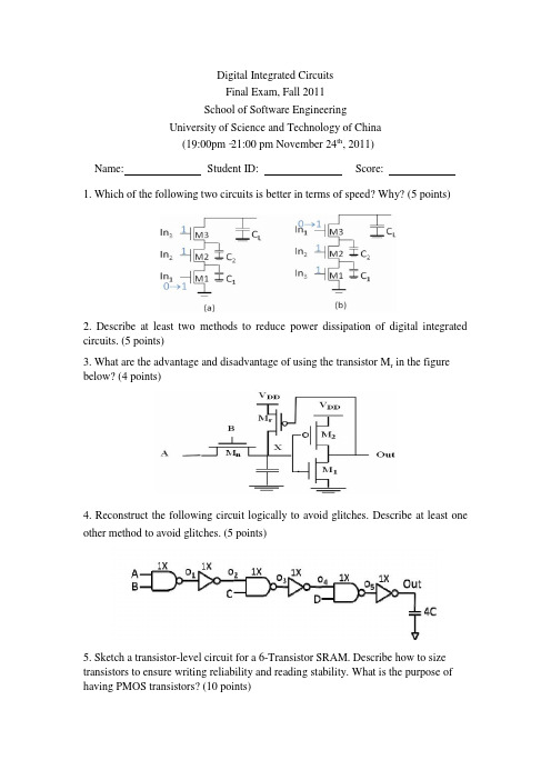
Digital Integrated CircuitsFinal Exam, Fall 2011School of Software EngineeringUniversity of Science and Technology of China(19:00pm–21:00 pm November24th, 2011)Name:Student ID:Score:1. Which of the following two circuits is better in terms of speed? Why?(5 points)2. Describe at least two methods to reduce power dissipation of digital integrated circuits. (5 points)3. What are the advantage and disadvantage of using the transistor M r in the figure below? (4 points)4.Reconstruct the following circuit logically to avoid glitches.Describe at least one other method to avoid glitches. (5 points)5.Sketch a transistor-level circuit for a 6-Transistor SRAM. Describe how to size transistors to ensure writing reliability and reading stability.What is the purpose of having PMOS transistors? (10 points)6.Consider a 24-bit, 6 stage carry-bypass adder with the following delays: t setup=4, t carry=1, t sum=4, t bypass=2.b) Consider the setup delay and carry propagation of the2nd, 3rd, and 4th stages.It is not on the critical path and can be made slower without affecting performance. If each stage is allowed to handle a different number of bits,how many bits would you assign to each of the first four stages to minimize the delay from inputs to the carry outputfor the first16 bits of the adder?(6 points)c)Given the condition that the number of bits in the last two stages is 8, how many bits would you assign to each of the last two stages to minimize the delay of the adder?(4 points)7. Assume the registers in the following figure are edge triggered with t clk-q, max= 4ns, t clk-q, min = 2ns, t setup = 1ns, and t hold= 1ns:CLK(a) What is the maximum operating frequency of this system if there is no skew and jitter? (8 points)(b) What is the maximum random clock skew that this system can tolerate? (6 points)8.Throughout this problem assume that the drain capacitance in the following figure,C D = 0.a) Assuming P(A=0)= P(B=0) = P(C=0) = P(D=0)=0.5, what are the activity factors (i.e.,α0→1) at each of the nodes n0– n3?(6 points)b) Assuming the circuit operates with a supply voltage V DD and a clock frequency f, what is the total dynamic power consumed by this circuit as a function of Cin, C1, C2, and C L (as labeled above)? Note that you should include the power dissipated by driving the A, B, C, and D inputs.(7 points)c)Using the method of logical effort, calculate the delay from A to n2 ((in units of t inv) as a function of Cin, C1, C2, and CL.(5 points)9. Sketch a transistor-level circuit for a master-slave positive edge-triggered register which consists of transmission gates. Express t setup and t hold in terms of t pd_inv(the delay of an inverter) and t pd_tx (the delay of a transmission gate). (7 points)10.What is the logic function performed by this circuit? What is the purpose of having the transistor M1? (4 points)11. Assume that the threshold voltage of NMOS transistors V TN = 0.4V. Calculate the voltage of nodes A and B respectively? (4 points)12.Consider the figure below. During the precharge phase, the output node is precharged to V DD. Assume that all inputs are set to zeros during precharge, and that the capacitance C a is discharged。
第一学期《数字电子技术》课程期末考试试卷A和答案数字电路与逻辑设计

北京信息科技大学2008~2009学年第一学期《数字电子技术》课程期末考试试卷A课程所在学院:自动化学院适用专业班级:测控0601-03考试形式:闭卷注意:所有答案写在答题纸上,写在试卷上无效。
一、填空题(本题满分20分,共含10道小题,每小题2分)1∙(7AC1)16=( )2=( 1=( )]0。
2.具有推挽式输出级的TT1电路(是/否)可以将输出端并联使用,普通的CMOS门(是/否)可以将输出端并联使用。
(输入端的状态均为不定)3.相同编号的最小项和最大项存在的关系为o4.(+1oo"的原码为,反码为,补码为o5.若A是逻辑变量,则A㊉I=。
二、逻辑函数式的化筒(12分)1 .利用公式法化简为最简与或式:F=AB∖A f CD+(AD+3'C')')(4+B)2 .利用卡诺图法将逻辑函数化简为最简与或式:y(A,B,G=>z(OJ2,4),给定约束条件为m3+rτ‰t+mβ+rr‰j=O下面电路图中,写出输出信号是什么状态(高电平、低电平或高阻态),已知乂为74系四、试用一片8选1数据选择器74HC151产生逻辑函数:Y=AB r CD÷48(C÷r>)+ABXCΦZ))÷ABC r 要求给出设计的全过程,并画出逻辑电路图。
(12分)s ,A2A4YO O O OO O O1O∣O O1O D1O O11O1O OO1O1/人O11O2O11151X X X高阻五、TT1主从JK触发器的输入波形如图所示,画出输出端Q的波形(12分)CP六、分析如图时序逻辑电路的逻辑功能,写出电路的驱动方程、状态方程和输出方程,画出电路的状态转换图,说明电路的功能以及能否自启动。
(14分)CP七、 试用一片4位同步二进制计数器741S163接成十进制计数器(允许附加必要的门电路,采用清零法),并作简要说明。
741S163的引脚图如下所示。
期末考试数字电子技术试题及答案(DOC)
数字电子技术基础试题(一)一、填空题 : (每空1分,共10分)1. (30.25) 10 = ( ) 2 = ( ) 16 。
2 . 逻辑函数L = + A+ B+ C +D = 。
3 . 三态门输出的三种状态分别为:、和。
4 . 主从型JK触发器的特性方程= 。
5 . 用4个触发器可以存储位二进制数。
6 . 存储容量为4K×8位的RAM存储器,其地址线为条、数据线为条。
二、选择题: (选择一个正确的答案填入括号内,每题3分,共30分 )1.设图1中所有触发器的初始状态皆为0,找出图中触发器在时钟信号作用下,输出电压波形恒为0的是:()图。
图 12.下列几种TTL电路中,输出端可实现线与功能的电路是()。
A、或非门B、与非门C、异或门D、OC门3.对CMOS与非门电路,其多余输入端正确的处理方法是()。
A、通过大电阻接地(>1.5KΩ)B、悬空C、通过小电阻接地(<1KΩ)D、通过电阻接V CC4.图2所示电路为由555定时器构成的()。
A、施密特触发器B、多谐振荡器C、单稳态触发器D、T触发器5.请判断以下哪个电路不是时序逻辑电路()。
图2A、计数器B、寄存器C、译码器D、触发器6.下列几种A/D转换器中,转换速度最快的是()。
图2A、并行A/D转换器B、计数型A/D转换器C、逐次渐进型A/D转换器D、双积分A/D转换器7.某电路的输入波形 u I 和输出波形 u O 如图 3所示,则该电路为()。
图3A、施密特触发器B、反相器C、单稳态触发器D、JK触发器8.要将方波脉冲的周期扩展10倍,可采用()。
A、10级施密特触发器B、10位二进制计数器C、十进制计数器D、10位D/A转换器9、已知逻辑函数与其相等的函数为()。
A、B、C、D、10、一个数据选择器的地址输入端有3个时,最多可以有()个数据信号输出。
A、4B、6C、8D、16三、逻辑函数化简(每题5分,共10分)1、用代数法化简为最简与或式Y= A +2、用卡诺图法化简为最简或与式Y= + C +A D,约束条件:A C + A CD+AB=0四、分析下列电路。
电子科大数字电路,期末试题101102半期考试试卷-答案
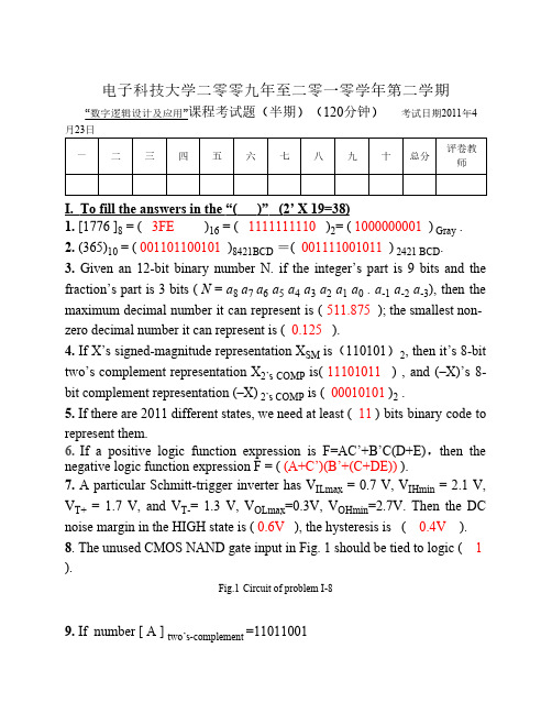
电子科技大学二零零九年至二零一零学年第二学期“数字逻辑设计及应用”课程考试题(半期)(120分钟)考试日期2011年4月23日一二三四五六七八九十总分评卷教师I. To fill the answers in the “( )” (2’ X 19=38)1. [1776 ]8 = ( 3FE )16 = ( 1111111110 )2= ( 1000000001 ) Gray .2. (365)10 = ( 001101100101 )8421BCD=( 001111001011 ) 2421 BCD.3.Given an 12-bit binary number N. if the integer’s part is 9 bits and the fraction’s part is 3 bits ( N = a8 a7 a6 a5 a4 a3 a2 a1 a0 . a-1 a-2 a-3), then the maximum decimal number it can represent is ( 511.875 ); the smallest non-zero decimal number it can represent is ( 0.125 ).4. If X’s signed-magnitude representation X SM is(110101)2, then it’s 8-bit two’s complement representation X2’s COMP is( 11101011 ) , and (–X)’s 8-bit complement representation (–X) 2’s COMP is ( 00010101 )2 .5. If there are 2011 different states, we need at least ( 11 ) bits binary code to represent them.6.If a positive logic function expression is F=AC’+B’C(D+E),then the negative logic function expression F = ( (A+C’)(B’+(C+DE)) ).7. A particular Schmitt-trigger inverter has V ILmax = 0.7 V, V IHmin = 2.1 V, V T+= 1.7 V, and V T-= 1.3 V, V OLmax=0.3V, V OHmin=2.7V. Then the DC noise margin in the HIGH state is ( 0.6V ), the hysteresis is ( 0.4V ). 8.The unused CMOS NAND gate input in Fig. 1 should be tied to logic ( 1 ).Fig.1Circuit of problem I-89. If number [ A ] two’s-complement =11011001and [ B] two’s-complement=10011101 , calculate[-A-B ]two’s-complement, [-A+B ]two’s-complement and indicate whether or not overflow occurs.[-A-B ] two’s-complement=[ 10001010 ], overflow: [ yes ][-A+B ] two’s-complement=[ 11000100 ], overflow: [ no ].10.The following logic diagram Fig.2 implements a function of 3-variable with a 74138. The logic function can be expressed as F (A,B,C) = ∑A,B,C ( 0,1,2 ).Fig.2 Circuit of problem I-10II. There is only one correct answer in the following questions.(3’ X 9 = 27)1. Which of the following Boolean equations is NOT correct? ( B )A) A+0=A B) A1 = AC) D)2. Suppose A2’s COMP =(1011),B2’s COMP =(1010),C2’s COMP =(0010). In the following equations, the most unlikely to produce overflow is( C )。
数字电子技术试题库及答案期末考试秘籍

数字电子技术期末试题库一、选择题:A组:1.如果采用偶校验方式,以下接收端收到的校验码中,〔 A 〕是不正确的A、00100B、10100C、11011D、111102、某一逻辑函数真值表确定后,下面描述该函数功能的方法中,具有唯一性的是〔B〕A、逻辑函数的最简及或式B、逻辑函数的最小项之和C、逻辑函数的最简或及式D、逻辑函数的最大项之和3、在以下逻辑电路中,不是组合逻辑电路的是〔D〕A、译码器B、编码器C、全加器D、存放器4、以下触发器中没有约束条件的是〔D〕A、根本RS触发器B、主从RS触发器C、同步RS触发器D、边沿D触发器5、555定时器不可以组成D。
A.多谐振荡器B.单稳态触发器C.施密特触发器D.J K触发器6、编码器〔A〕优先编码功能,因而〔C〕多个输入端同时为1。
A、有B、无C、允许D、不允许7、〔D〕触发器可以构成移位存放器。
A、根本RS触发器B、主从RS触发器C、同步RS触发器D、边沿D触发器8、速度最快的A/D转换器是〔A〕电路A、并行比拟型B、串行比拟型C、并-串行比拟型D、逐次比拟型9、某触发器的状态转换图如下图,该触发器应是( C )A. J-K触发器B. R-S触发器C. D触发器D. T触发器10.〔电子专业作〕对于VHDL以下几种说法错误的选项是〔A 〕A VHDL程序中是区分大小写的。
B 一个完整的VHDL程序总是由库说明局部、实体和构造体等三局部构成C VHDL程序中的实体局部是对元件和外部电路之间的接口进展的描述,可以看成是定义元件的引脚D 构造体是描述元件内部的构造和逻辑功能B组:1、微型计算机和数字电子设备中最常采用的数制是--------------------------------〔 A 〕2、十进制数6在8421BCD码中表示为-------------------------------------------------〔 B 〕A.0101B.0110C. 0111D. 10003、在图1所示电路中,使__AY 的电路是---------------------------------------------〔 A 〕A. ○1B. ○2C. ○3D. ○44、接通电源电压就能输出矩形脉冲的电路是------------------------------------------〔 D 〕A. 单稳态触发器B. 施密特触发器C. D触发器D. 多谐振荡器5、多谐振荡器有-------------------------------------------------------------------------------〔 C 〕A. 两个稳态B. 一个稳态C. 没有稳态D. 不能确定6、输入A、B和输出Y的波形如以下图所示,则对应的逻辑门电路是-------〔 D 〕A. 及门B. 及非门C. 或非门D. 异或门7、以下电路中属于时序逻辑电路的是------------------------------------------------------〔 B 〕A. 编码器B. 计数器C. 译码器D. 数据选择器8、在某些情况下,使组合逻辑电路产生了竞争及冒险,这是由于信号的---------〔 A 〕A. 延迟B. 超前C. 突变D. 放大9、以下哪种触发器可以方便地将所加数据存入触发器,适用于数据存储类型的时序电路--------------------------------------------------------------------------------〔 C 〕A. RS触发器B. JK触发器C. D触发器D. T触发器10、电路和波形如以下图,正确输出的波形是-----------------------------------------------〔 A 〕A. ○1B. ○2C. ○3D. ○4C组:1.十进制数25用8421BCD码表示为 A 。
数字电子技术期末考试题及答案(经典)
xxx~xxx学年第x学期《数字电子技术》期末复习题第一部分题目一、判断题(每题2分,共30分。
描述正确的在题号前的括号中打“√”,错误的打“×”)【】1、二进制有0 ~ 9十个数码,进位关系为逢十进一。
【】2、(325)8 >(225)10【】3、十进制数整数转换为二进制数的方法是采用“除2取余法”。
【】4、在二进制与十六进制的转换中,有下列关系:(100111010001)2=(9D1)16【】5、8421 BCD码是唯一能表示十进制数的编码。
【】6、十进制数85的8421 BCD码是101101。
【】7、格雷码为无权码,8421 BCD为有权码。
【】8、数字电路中用“1”和“0”分别表示两种状态,二者无大小之分。
【】9、逻辑变量的取值,1比0大。
【】10、在逻辑代数中,逻辑变量和函数均只有0和1两个取值,且不表示数量的大小。
【】11、逻辑运算1+1=1【】12、逻辑运算A+1+0=A【】13、因为逻辑表达式A+B+AB=A+B成立,所以AB=0成立。
【】14、在时间和幅度上均不连续的信号是数字信号,所以语音信号是数字信号。
【】15、逻辑函数的运算次序为:先算括号内,后算括号外;先求与,再求或,最后求非。
【】16、AB A C BC AB A C++=+【】17、逻辑函数表达式的化简结果是唯一的。
【】18、逻辑真值表、逻辑表达式、逻辑图均是逻辑关系的描述方法。
【】19、n个变量组成的最小项总数是2n个。
【】20、逻辑函数的化简方法主要有代数化简法和卡诺图化简法。
【】21、逻辑函数化简过程中的无关项一律按取值为0处理。
【】22、数字电路中晶体管工作在开关状态,即不是工作在饱和区,就是工作在截止区。
【】23、TTL或非门的多余输入端可以接高电平。
【】24、某一门电路有三个输入端A、B、C,当输入A、B、C不全为“1”时,输出Y为“0”,输入A、B、C全为高电平“1”时,输出Y为“1”,此门电路是或门电路。
数电期末试卷及答案共4套

大学信息院数字电子技术根底期终考试试题〔110分钟〕(第一套)一、填空题:〔每空1分,共15分〕1.逻辑函数Y AB C=+的两种标准形式分别为〔〕、〔〕。
2.将2004个“1〞异或起来得到的结果是〔〕。
3.半导体存储器的构造主要包含三个局部,分别是〔〕、〔〕、〔〕。
4.8位转换器当输入数字量10000000为5v。
假设只有最低位为高电平,那么输出电压为〔〕v;当输入为10001000,那么输出电压为〔〕v。
5.就逐次逼近型与双积分型两种转换器而言,〔〕的抗干扰能力强,〔〕的转换速度快。
6.由555定时器构成的三种电路中,〔〕与〔〕是脉冲的整形电路。
7.及相比,器件有可编程的输出构造,它是通过对〔〕进展编程设定其〔〕的工作模式来实现的,而且由于采用了〔〕的工艺构造,可以重复编程,使它的通用性很好,使用更为方便灵活。
二、根据要求作题:〔共15分〕1.将逻辑函数写成“及或非〞表达式,并用“集电极开路及非门〞来实现。
2.图1、2中电路均由门电路构成,写出P、Q 的表达式,并画出对应A、B、C的P、Q波形。
三、分析图3所示电路:〔10分〕1)试写出8选1数据选择器的输出函数式;2)画出A2、A1、A0从000~111连续变化时,Y的波形图;3)说明电路的逻辑功能。
四、设计“一位十进制数〞的四舍五入电路〔采用8421码〕。
要求只设定一个输出,并画出用最少“及非门〞实现的逻辑电路图。
〔15分〕五、电路及、A的波形如图4(a) (b)所示,设触发器的初态均为“0〞,试画出输出端B与C的波形。
〔8分〕BC六、用T触发器与异或门构成的某种电路如图5(a)所示,在示波器上观察到波形如图5(b)所示。
试问该电路是如何连接的?请在原图上画出正确的连接图,并标明T的取值。
〔6分〕七、图6所示是16*4位与同步十六进制加法计数器74161组成的脉冲分频电路。
中的数据见表1所示。
试画出在信号连续作用下的D3、D2、D1、D0输出的电压波形,并说明它们与信号频率之比。
数字电子技术_期末考试试题(5套)
期末考试试题课程名称 《数字电子技术》 适用专业自动化、测控 考试时间 ( 120 )分钟一、 填空题(22分每空2分)1、=⊕0A , =⊕1A 。
2、JK 触发器的特性方程为: 。
3、单稳态触发器中,两个状态一个为 态,另一个为 态.多谐振荡器两个状态都为 态, 施密特触发器两个状态都为 态.4、组合逻辑电路的输出仅仅只与该时刻的 有关, 而与 无关。
5、某数/模转换器的输入为8位二进制数字信号(D 7~D 0),输出为0~25.5V 的模拟电压。
若数字信号的最低位是“1”其余各位是“0”,则输出的模拟电压为 。
6、一个四选一数据选择器,其地址输入端有 个。
二、 化简题(15分 每小题5分)用卡诺图化简逻辑函数,必须在卡诺图上画出卡诺圈1) Y (A,B,C,D )=∑m (0,1,2,3,4,5,6,7,13,15)2)∑∑+=)11,10,9,3,2,1()15,14,13,0(),,,(d m D C B A L 利用代数法化简逻辑函数,必须写出化简过程3)__________________________________________________)(),,(B A B A ABC B A C B A F +++=三、 画图题(10分 每题5分)据输入波形画输出波形或状态端波形(触发器的初始状态为0). 1、2、四、 分析题(17分)1、分析下图,并写出输出逻辑关系表达式,要有分析过程(6分)2、电路如图所示,分析该电路,画出完全的时序图,并说明电路的逻辑功能,要有分析过程(11分)五、设计题(28分)1、用红、黄、绿三个指示灯表示三台设备的工作情况:绿灯亮表示全部正常;红灯亮表示有一台不正常;黄灯亮表示两台不正常;红、黄灯全亮表示三台都不正常。
列出控制电路真值表,要求用74LS138和适当的与非门实现此电路(20分)2、中规模同步四位二进制计数器74LS161的功能表见附表所示;请用反馈预置回零法设计一个六进制加法计数器。
电子科技大学数字逻辑电路期末考试题

………密………封………线………以………内………答………题………无………效……电子科技大学二零零七年至二零零八学年第一学期期末一、填空题 (每题1.5分,共15分)1、已知74LS 系列的V OL max = 0.5 V , V OH min = 2.7 V , V IL max = 0.8 V, V IH min = 2.0 V , 则直流噪声容限是( )。
2、若EPROM 的容量为512K 字×8位,则地址码应取( )位。
3、b n⨯2 EPROM 可视为存储一个( )输入( )输出的真值表。
4、CMOS 门电路中,NMOS 的串联可实现( )操作,NMOS 的并联可实现( )操作。
5、已知带符号二进制反码为 ( 001101) 2 , 问 对应的8-bit 的补码为 ( ) 2.6、DAC 的功能是将输入的( )成正比地转换成( )输出。
7、CMOS 或非门的未用输入端应连接到( )电平上。
二、判断题 (每题1分,共5分)1、 ( )仅由与非门构成的电路是组合逻辑电路。
2、 ( )若)7,3,1(,,C B A F ∏=,则)7,3,1(,,'C B A F ∑= 3、 ( )具有n 个输入、m 个输出、p 个触发器的状态机有pn +2个状态。
4、 ( )1个“1”与1000个“0”的同或(异或非)运算,结果为“1”。
5、 ( )若AC AB ≠,则C B ≠。
三、(1)将F 1函数进行卡诺图化简,并以或非/或非结构予以实现。
(5分)∑∑+=),(),,,,,(98d 13127654m F 1………密………封………线………以………内………答………题………无………效……(2)将F 2函数进行卡诺图化简,并以与非/与非结构予以实现。
(5分)),,,,,,,(14121196431M F 2∏=四、现有下列真值表,其中A2、A1、A0是电路的输入, D1和D0是电路的输出。
电子科技大学数字电路期末考试样题

图1一、填空题1.五个变量构成的所有最小项之和等于 ( )。
2.已知某数的二进制原码表示为 ( 110110) 2 , 则其对应的8-bit 补码表示为 ( )2。
3.已知∑=C B A F,,)3,0(,则∑='C B A F ,,( )。
4.要使D 触发器按'*Q Q =工作,则D 触发器的输入D=( )。
5.用移位寄存器产生1101010序列,至少需要( )位的移位寄存器。
二、单项选择题:1. 若要将一异或门当作反相器(非门)使用,则输入端A 、B 端的连接方式是( )。
A. A 或B 中有一个接“0”B. A 或B 中有一个接“1”C. A 和B 并联使用D. 不能实现 2.组合电路的竞争冒险是由于( )引起的。
A. 电路不是最简B. 电路有多个输出C. 电路中使用不同的门电路D. 电路中存在延时3.某一逻辑函数真值表确定后,下面描述该函数逻辑功能的表达式中,具有唯一性的是( )。
A .该逻辑函数的最简与或式B .该逻辑函数的积之和标准型C .该逻辑函数的最简或与式D .该逻辑函数的和之积式4.若最简状态转换表中,状态数为n ,则所需状态变量数K 为 ( )的整数.A .n K 2log =B .n K 2log <C . n K 2log ≥D . n K 2log ≤5.某计数器的状态转换图如图1所示,其该计数器的模为( )。
A . 八 B. 五 C. 四 D. 三 三、 组合电路分析:1.求逻辑函数Z Y X Y X Z X F ⋅'⋅+⋅+⋅'= 的最简积之和表达式。
2.已知逻辑函数∑=Z Y X F,,)7,5,1(, 请写出该函数的标准和(最小项之和)表达式:3.找出逻辑表达式X W Y W F ⋅+'⋅'=对应的电路的所有静态冒险。
四、组合电路设计:1、试用一片三输入八输出译码器74X138和适当的与非门实现函数:画出电路连接图。
数字电子技术期末复习题库及答案(1).doc
第1单元能力训练检测题一、填空题1、由二值变量所构成的因果关系称为逻辑关系。
能够反映和处理逻辑关系的数学工具称为逻辑代数。
2、在正逻辑的约定下,“1”表示高电平,“0”表示低电平。
3、数字电路中,输入信号和输出信号之间的关系是逻辑关系,所以数字电路也称为逻辑电路。
在逻辑关系中,最基本的关系是与逻辑、或逻辑和非逻辑。
4、用来表示各种计数制数码个数的数称为基数 ,同一数码在不同数位所代表的权不同。
十进制计数各位的基数是10, 位权是10的幂。
5、 8421 BCD码和 2421 码是有权码;余3 码和格雷码是无权码。
6、进位计数制是表示数值大小的各种方法的统称。
一般都是按照进位方式来实现计数的,简称为数制。
任意进制数转换为十进制数时,均采用按位权展开求和的方法。
7、十进制整数转换成二进制时采用除2取余法;十进制小数转换成二进制时采用乘2取整法。
8、十进制数转换为八进制和十六进制时,应先转换成二进制,然后再根据转换的二进数,按照三个数码一组转换成八进制;按四个数码一组转换成十六进制。
9、逻辑代数的基本定律有交换律、结合律、分配律、反演律和非非律。
10、最简与或表达式是指在表达式中与项中的变量最少,且或项也最少。
13、卡诺图是将代表最小项的小方格按相邻原则排列而构成的方块图。
卡诺图的画图规则:任意两个几何位置相邻的最小项之间,只允许一位变量的取值不同。
14、在化简的过程中,约束项可以根据需要看作 1 或 0 。
二、判断正误题1、奇偶校验码是最基本的检错码,用来使用PCM方法传送讯号时避免出错。
(对)2、异或函数与同或函数在逻辑上互为反函数。
(对)3、8421BCD码、2421BCD码和余3码都属于有权码。
(错)4、二进制计数中各位的基是2,不同数位的权是2的幂。
(对)3、每个最小项都是各变量相“与”构成的,即n个变量的最小项含有n个因子。
(对)4、因为逻辑表达式A+B+AB=A+B成立,所以AB=0成立。
电子科技大学模电试卷A卷(2011-12)答案

………密………封………线………以………内………答………题………无………效……电子科技大学2011-2012学年第一学期期末考试A 卷课程名称:模拟电路和脉冲电路基础考试形式:闭卷考试日期:2012年1月11日考试时长:120分钟课程成绩构成:平时20 %,期中20 %,实验0 %,期末60 %本试卷试题由三部分构成,共5 页。
一、简答题(共30分,共6题,每题5分)1、简述常用的电压放大器与功率放大器的不同点?1)任务不同:电压放大—不失真地提高输入信号的幅度,以驱动后面的功率放大级,通常工作在小信号状态。
(2分)功率放大—信号不失真或轻度失真的条件下提高输出功率,通常工作在大信号状态。
(2分)2)分析方法不同:电压放大—采用微变等效电路法和图解法;功率放大—图解法。
(1分)2、简述引入负反馈改善波形失真的原因?失真的反馈信号(1分),使净输入产生相反的失真(2分),从而弥补了放大电路本身的非线性失真。
(2分)3、什么叫脉冲电路?简述脉冲电路构成和常见脉冲电路?脉冲电路是用来产生和处理脉冲信号的电路。
(1分)脉冲电路可以用分立晶体管、场效应管作为开关和RC或RL电路构成,也可以由集成门电路或集成运算放大器和RC充、放电电路构成。
(2分)常用的有脉冲波形的产生、变换、整形等电路,如双稳态触发器、单稳态触发器、自激多谐振荡器、射极耦合双稳态触发器(施密特电路)及锯齿波电路。
(2分)………密………封………线………以………内………答………题………无………效……4、一般地,CE 、CC 和CB 晶体管基本放大电路的带宽哪个最小?哪个最大?一般地,基本的BJT 共射放大器的带宽最小(2分),共集放大器的带宽最大(3分)。
5、简述乙类互补对称电路交越失真产生的原因,如何进行克服?当输入信号vi 在0~V BE 之间变化时,不足以克服死区电压,三极管不工作。
因此在正、负半周交替过零处会出现一些非线性失真,这个失真称为交越失真。
- 1、下载文档前请自行甄别文档内容的完整性,平台不提供额外的编辑、内容补充、找答案等附加服务。
- 2、"仅部分预览"的文档,不可在线预览部分如存在完整性等问题,可反馈申请退款(可完整预览的文档不适用该条件!)。
- 3、如文档侵犯您的权益,请联系客服反馈,我们会尽快为您处理(人工客服工作时间:9:00-18:30)。
………密………封………线………以………内………答………题………无………效……
电子科技大学2010 -2011学年第二学期期末考试 A 卷
课程名称:_数字逻辑设计及应用__ 考试形式:闭卷考试日期:20 11 年7 月7 日考试时长:_120___分钟
课程成绩构成:平时30 %,期中30 %,实验0 %,期末40 %
本试卷试题由__六___部分构成,共__6___页。
I. Fill your answers in the blanks (3’ X 10=30’)
1. A parity circuit with N inputs need N-1XOR gate s. If the number of “1” in an N logic variables set, such as A、B、C、…W, is even number, then__________
A B C W
⊕⊕⊕⋅⋅⋅⋅⊕=0 .
2. A circuit with 4 flip-flops can store 4bit binary numbers, that is, include 16 states at most.
3. A modulo-20 counter circuit needs 5 D filp-flops at least. A modulo-288 counter circuit needs 3 4-bit counters of 74x163 at least.
4. A 8-bit ring counter has 8 normal states. If we want to realize the same number normal states, we need
a 4bit twisted-ring counter.
5. If the input is 10000000 of an 8 bit DAC, the corresponding output is 5v. Then an input is 00000001 to the DAC, the corresponding output is 5/128 (0.0391) V; if an input is 10001000, the corresponding DAC output is 5.3125V.
………密………封………线………以………内………答………题………无………效……
II. Please select the only one correct answer in the following questions.(2’ X 5=10)
1. We need ( B ) chips of 4K ⨯4 bits RAM to form a 16 K ⨯ 8 bits RAM.
A) 2 B) 8 C) 4 D) 16
2. To design a "01101100" serial sequence generator by shift registers, we need a
( A )-bit shift register as least.
A) 5 B) 4 C) 3 D) 6
3. For the following latches or flip-flops, ( B ) can be used to form shift register.
A) S-R latch B) master-slave flip-flop C) S-R latch with enable D) S ’-R ’ latch 4. Which of the following statements is correct? ( C )
A) The outputs of a Moore machine depend on inputs as well as the states. B) The outputs of a Mealy machine depend only on the states.
C) The outputs of a Mealy machine depend on inputs as well as the states. D) A), B), C) are wrong.
5. There is a state/output table of a sequential machine as the table 1, what the input sequences is detected?
( D )
A) 11110 B) 11010 C) 10010 D) 10110
Table 1
………密………封………线………以………内………答………题………无………效……
III.
Analyze the sequential-circuit as shown in figure 1. [15’]
1. Write out the excitation equations, transition equations and output equation. [5’]
2. Assume the initial state is Q 2Q 1=00, complete the timing diagram for Q 2 ,Q 1 and Z.( Don ’t need consider
propagation delay of each component) [10’]
Figure-1
解答:
激励方程: D 1=Q 1⊕Q 2,D 2= Q /1+ Q /2 转移方程:Q 1 *= D 1=Q 1⊕Q 2,Q 2 *=D 2= Q /1+ Q /2 输出方程:Z= Q 1•Q 2
………密………封………线………以………内………答………题………无………效……
IV.Design a Mealy sequential detector with one input x and one output z. If and only if x continues to be 1111 or 1001, the output z is 1. Otherwise, the output z is 0. The overlap is permitted. Please describe the state meaning and finish the state/output table. [15]
Example:x:0 1 0 1 1 1 1 0 0 1 1 0 0 1 1 1 1 1
z:0 0 0 0 0 0 1 0 0 1 0 0 0 1 0 0 1 1
X
State meaning S 0 1
Initial A A,0 B,0
Received 1 B C,0 D,0
Received 10 C E,0 B,0
Received 11 D C,0 F,0
Received 100 E A,0 B,1
Received 111 F C,0 F,1
S*,Z
………密………封………线………以………内………答………题………无………效……
V . Analyze the circuit as shown below, which contains a 74x163 4-bit binary counter, a 74x138
decoder and a 74x153 4-input,1-bit multiplexer. When control input MN=10 for 74x153 multiplexer, [15’] 1. Write out the logic expression of 74x153’ output F. [5’]
2. Write out the sequence of states for the 74x161 in the circuit. [7’]
3. Describe the modulus(模) of the circuit. [3’]
解答:
F=D2=Y6/=(QDQCQBQA /)/
状态序列:0,1,2,3,4,5,6,7,8,9,10,11,12,13,14,0,1,2,… M=15
………密………封………线………以………内………答………题………无………效……
VI. Design a minimal-cost modulo-5 synchronous counter with D flip-flops and necessary gates,
the state transition sequence is 0→2→4→1→3→0→…with the binary code. [15’] 1. Fill out the transition/output table. [8’]
2. Write out the excitation equations and output equation. [4’]
3. List the complete transition/output table, and check the self-correct. [3’] transition/output table : complete transition/output table:
激励方程:D2=Q1⋅Q0’ D1= Q2’⋅Q1’ D0= Q2+Q1’⋅Q0 输出方程:Z=Q1Q0
检查自启动:当Q2Q1Q0=101,可得下一状态为001;当Q2Q1Q0=110,可得下一状态为101;当Q2Q1Q0=111,可得下一状态为001。
电路能够自启动。