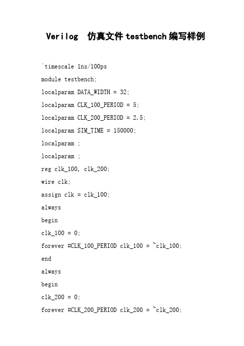
Verilog仿真文件testbench编写样例
verilogtestbench写法

verilogtestbench写法Verilog测试平台(testbench)技术(⼀) 收藏对设计进⾏功能仿真和时序仿真时,需要给待测模块提供激励输⼊。
对于由Verilog语⾔描述的设计模块,最好的⽅法⾃然同样是⽤Verilog语⾔对待测模块施加激励和检测模块的输出响应。
实际应⽤中,Verilog测试平台(testben ch)就是⽤来提供上述功能的。
Verilog测试平台是⼀个例化的待测(MUT)Verilog 模块,给它施加激励并观测其输出。
由于测试平台是⽤Verilog语⾔描述的,因此可以应⽤到不同的仿真环境中。
待测模块和与之对应的测试平台组成⼀个仿真模型,应⽤这个模型可以在不同的测试环境中⽤相同的激励对待测模块进⾏调试。
下⾯就对不同电路类型分别介绍verilog测试平台的语⾔结构。
⼀、测试平台1.组合电路测试设计组合电路的测试平台时,待测模块及其功能决定了激烈的选择与测试次数。
对于⼀个已有的待测模块,测试平台中需要声明与待测模块输⼊输出端⼝对应的变量。
与输⼊端⼝相连接的变量定义为reg,与输出端⼝相连接的变量定义为wire,例化时将测试平台中声明的变量与待测模块的输⼊输出端⼝相关联。
使⽤initial语句控制程序运⾏,initial语句是⼀种过程结构,在initial块中可使⽤延迟控制语句来控制initial块中的程序流动。
这⾥对⼀个简单的算术逻辑单元(ALU)为例进⾏测试,下⾯是该单元Verilog 描述。
/***************************************************************** ********///多动能ALU的Verilog代码'timescale 1ns/100psmodule alu_4bit(a,b,f,oe,y,p,ov,a_gt_b,a_eg_b,a_lt_b);input [3:0] a,b;input [1:0] f;input oe;input [3:0] y;output p,ov,a_gt_b,a_eg_b,a_lt_b; reg [4:0] im_y;always @(a or b or f)beginov=1'b0;im_y=0;case(f)2'b00:beginim_y=a+b;if(im_y>5'b01111)ov=1'b1;end2'b01:beginim_y=a-b;if(im_y>5'b01111)ov=1'b1;end2'b10:im_y[3:0]=a&b;2'b11:im_y[3:0]=a^b;default:im_y[3:0]=4'b0000;endcaseendalways @(a or b)beginif(a>b){a_gt_b,a_ge_b,a_lt_b}=3'b100;else if(a{a_gt_b,a_ge_b,a_lt_b}=3'b001;else{a_gt_b,a_ge_b,a_lt_b}=3'b010;endassign p=^im_y[3:0];assign y=oe?im_y[3:0]:4'bz;endmodule/***************************************************************** ********/模块alu_4bit是四功能的算术逻辑单元,输⼊包括数据信号a、b和功能信号f,输出包括数据信号y和ALU⽣成的奇偶校验信号p、溢出信号ov及⽐较信号。
Verilog仿真文件testbench编写样例
Verilog 仿真文件testbench编写样例`timescale 1ns/100psmodule testbench;localparam DATA_WIDTH = 32;localparam CLK_100_PERIOD = 5;localparam CLK_200_PERIOD = 2.5;localparam SIM_TIME = 150000;localparam ;localparam ;reg clk_100, clk_200;wire clk;assign clk = clk_100;alwaysbeginclk_100 = 0;forever #CLK_100_PERIOD clk_100 = ~clk_100;endalwaysbeginclk_200 = 0;forever #CLK_200_PERIOD clk_200 = ~clk_200;endreg rstn;integer fp_testin;integer fp_matlab_out;integer fp_sim_out;integer fp_outdiff;reg signed [DATA_WIDTH/2-1:0] matlab_in_re, matlab_in_im;reg signed [DATA_WIDTH/2-1:0] matlab_out_re, matlab_out_im;reg signed [DATA_WIDTH/2-1:0] matlab_diff_re, matlab_diff_im;reg signed [DATA_WIDTH/2-1:0] matlab_diff_re2, matlab_diff_im2;reg signed [DATA_WIDTH/2-1:0] max_diff_re, max_diff_im;initial beginmax_diff_re = 0;max_diff_im = 0;rstn = 0;#500rstn = 1;#SIM_TIMEsim_finish();$stop();endtask sim_finish;beginif(fp_testin!=0)$fclose(fp_testin);if(fp_matlab_out!=0)$fclose(fp_matlab_out);if(fp_sim_out)$fclose(fp_sim_out);if(fp_outdiff!=0)$fclose(fp_outdiff);endendtaskinitialbeginfp_testin = 0;fp_testin=$fopen("txt_file/input_data.txt"," r");if(fp_testin==0)begin$display("input_data.txt open failed!"); sim_finish();$stop();endelse begin$fscanf(fp_testin,"%d, %d\n",matlab_in_re,matlab_in_im); endfp_matlab_out = 0;fp_matlab_out =$fopen("txt_file/matlab_out.txt"," r");if(fp_matlab_out==0)begin$display("fp_matlab_out.txt openfailed!");sim_finish();$stop();endelse begin$fscanf(fp_matlab_out,"%d, %d\n",matlab _out_re,matlab_out_im);endfp_sim_out = 0;fp_sim_out =$fopen("txt_file/modelsim_out.txt",&quo t;w");if(fp_sim_out == 0)begin$display("modelsim_out_re.txt openfailed!");sim_finish();$stop();endfp_outdiff = 0;fp_outdiff =$fopen("text_file/outdiff.txt","w& quot;);if(fp_outdiff==0)begin$display("outdiff.txt open failed!"); sim_finish();$stop();endendalways @(posedge clk)beginif(stest_wvalid && stest_wready) //ready to changebeginif(~$feof(fp_testin))$fscanf(fp_testin,"%d, %d\n",matlab_in_re,matlab_in_im); endelsebeginmatlab_in_re <= matlab_in_re;matlab_in_im <= matlab_in_im;endendalways @(posedge clk_100)beginif(mfc_wready && mfc_wvalid)beginmatlab_diff_re <= mfc_wdata_re - matlab_out_re; matlab_diff_im <= mfc_wdata_im - matlab_out_im; matlab_diff_re2 <= matlab_out_re - mfc_wdata_re ; matlab_diff_im2 <= matlab_out_im - mfc_wdata_im ; if(max_diff_re < matlab_diff_re)beginmax_diff_re <= matlab_diff_re;$display("max_diff_re:%dmax_diff_im:%d\n",max_diff_re,max_diff_im); endelse if(max_diff_re < matlab_diff_re2)beginmax_diff_re <= matlab_diff_re2;$display("max_diff_re:%dmax_diff_im:%d\n",max_diff_re,max_diff_im); endif(max_diff_im < matlab_diff_im)beginmax_diff_im <= matlab_diff_im;$display("max_diff_re:%dmax_diff_im:%d\n",max_diff_re,max_diff_im); endelse if(max_diff_im < matlab_diff_im2)beginmax_diff_im <= matlab_diff_im2;$display("max_diff_re:%dmax_diff_im:%d\n",max_diff_re,max_diff_im); end$fscanf(fp_matlab_out,"%d, %d\n",matlab _out_re,matlab_out_im);$fwrite(fp_sim_out, "%d, %d\n",mfc_wdata_re,mfc_wdata_im);$fwrite(fp_outdiff,"%d, %d\n",matlab_diff_re,matlab_diff_i m);endendendmodule。
编写高效率的testbench
编写高效率的testbench简介:由于设计的规模越来越大也越来越复杂,数字设计的验证已经成为一个日益困难和繁琐的任务。
验证工程师们依靠一些验证工具和方法来应付这个挑战。
对于几百万门的大型设计,工程师们一般使用一套形式验证(formal verification)工具。
然而对于一些小型的设计,设计工程师常常发现用带有testbench的HDL仿真器就可以很好地进行验证。
Testbench已经成为一个验证高级语言(HLL --High-Level Language) 设计的标准方法。
通常testbench完成如下的任务:1.实例化需要测试的设计(DUT);2.通过对DUT模型加载测试向量来仿真设计;3.将输出结果到终端或波形窗口中加以视觉检视;4.另外,将实际结果和预期结果进行比较。
通常testbench用工业标准的VHDL或Verilog硬件描述语言来编写。
Testbench调用功能设计,然后进行仿真。
复杂的testbench完成一些附加的功能—例如它们包含一些逻辑来选择产生合适的设计激励或比较实际结果和预期结果。
后续的章节描述了一个仔细构建的testbench的结构,并且提供了一个自动比较实际结果与预期结果的进行自我检查的testbench例子。
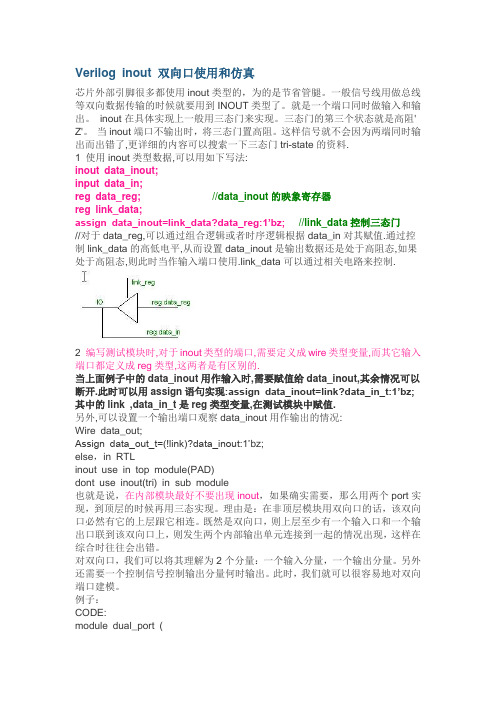
图1给出了一个如上所描述步骤的标准HDL验证流程。
由于testbench使用VHDL或Verilog来描述,testbench的验证过程可以根据不同的平台或不同的软件工具实现。
由于VHDL或Verilog是公开的通用标准,使用VHDL或Verilog编写的testbench以后也可以毫无困难地重用(reuse)。
图1使用Testbench的HDL验证流程构建TestbenchTestbench用VHDL或Verilog来编写。
由于testbench只用来进行仿真,它们没有那些适用于综合的RTL语言子集的语法约束限制,而是所有的行为结构都可以使用。
因而testbench可以编写的更为通用,使得它们可以更容易维护。
组合-时序逻辑电路Verilog-Testbench代码_带仿真代码和波形_

1组合逻辑电路--基本门电路1.1基本门电路1.1.1结构化描述方式代码如下View Code1 module logics2 (3 input iA,4 input iB,5 output oAnd,6 output oOr,7 output oNot8 );910 and and_inst(oAnd,iA,iB);11 or or_inst(oOr,iA,iB);12 not not_inst(oNot,iA);1314 endmodule最底层的是门级原语and or not RTL级视图testbench如下View Code1 `timescale 1 ns/ 1 ns2 module logics_tb();34 reg ia;5 reg ib;67 wire oAnd;8 wire oOr;9 wire oNot;1011 initial12 begin13 ia=0;14 #40 ia=1;15 #40 ia=0;16 #40 ia=1;17 #40 ia=0;18 end1920 initial21 begin22 ib=0;23 #40 ib=0;24 #40 ib=1;25 #40 ib=1;26 #40 ib=0;27 end2829 logics logics_inst30 (31 .iA(ia),32 .iB(ib),33 .oAnd(oAnd),34 .oOr(oOr),35 .oNot(oNot)36 );3738 endmoduleRTL级仿真图形如下GATE级仿真图如下可见RTL级仿真是理想的,GATE级仿真考虑了延迟和信号开始的不确定。
1.1.2采用流描述方法代码如下View Code1 module logics2 (3 input iA,4 input iB,5 output oAnd,6 output oOr,7 output oNot8 );910 assign oAnd=iA&iB;11 assign oOr=iA|iB;12 assign oNot=~iA;1314 endmoduleRTL级视图,仿真图形同上。
Verilog-testbench的写法

数字集成电路设计入门--从HDL到版图于敦山北大微电子学系第十五章Verilog Test Bench使用简介学习内容:•用一个复杂的test bench复习设计的组织与仿真•建立test bench通常使用的编码风格及方法设计组织虚线表示编译时检测输入文件是否存在及可读并允许生成输出文件。
test bench 组织stimulus要验证的设计简单的test bench•简单的test bench 向要验证的设计提供向量,人工验证输出。
•复杂的test bench 是自检测的,其结果自动验证。
复杂的test bench激励验证结果要验证的设计并行块•fork…join块在测试文件中很常用。
他们的并行特性使用户可以说明绝对时间,并且可以并行的执行复杂的过程结构,如循环或任务。
module inline_ tb;reg [7: 0] data_ bus;// instance of DUTinitial forkdata_bus = 8'b00;Time | data_ bus0 | 8’b0000_0000 10 | 8’b0100_0101 30 | 8’b0100_0110 40 | 8’b0100_0111 45 | 8’b1000_1110#10 data_bus = 8'h45;#20 repeat (10) #10 data_bus = data_bus + 1;#25 repeat (5) #20 data_bus = data_bus<< 1;#140 data_bus = 8'h0f;joinendmodule上面的两个repeat循环从不同时间开始,并行执行。
象这样的特殊的激励集在单个的begin…end块中将很难实现。
50 | 8’b1000_1111 60 | 8’b1001_0000 65 | 8’b0010_0000 70 | 8’b0010_0001 80 | 8’b0010_0010 85 | 8’b0100_0100 90 | 8’b0100_0101 100 | 8’b0100_0110 105 | 8’b1000_1100 110 | 8’b1000_1101 120 | 8’b1000_1110 125 | 8’b0001_1100 140 | 8’b0000_1111包含文件•包含文件用于读入代码的重复部分或公共数据。
Verilog中inout类型的数据的使用和testbench仿真写法
Verilog inout 双向口使用和仿真芯片外部引脚很多都使用inout类型的,为的是节省管腿。
一般信号线用做总线等双向数据传输的时候就要用到INOUT类型了。
就是一个端口同时做输入和输出。
inout在具体实现上一般用三态门来实现。
三态门的第三个状态就是高阻' Z'。
当inout端口不输出时,将三态门置高阻。
这样信号就不会因为两端同时输出而出错了,更详细的内容可以搜索一下三态门tri-state的资料.1 使用inout类型数据,可以用如下写法:inout data_inout;input data_in;reg data_reg;//data_inout的映象寄存器reg link_data;assign data_inout=link_data?data_reg:1’bz;//link_data控制三态门//对于data_reg,可以通过组合逻辑或者时序逻辑根据data_in对其赋值.通过控制link_data的高低电平,从而设置data_inout是输出数据还是处于高阻态,如果处于高阻态,则此时当作输入端口使用.link_data可以通过相关电路来控制.2 编写测试模块时,对于inout类型的端口,需要定义成wire类型变量,而其它输入端口都定义成reg类型,这两者是有区别的.当上面例子中的data_inout用作输入时,需要赋值给data_inout,其余情况可以断开.此时可以用assign语句实现:assign data_inout=link?data_in_t:1’bz;其中的link ,data_in_t是reg类型变量,在测试模块中赋值.另外,可以设置一个输出端口观察data_inout用作输出的情况:Wire data_out;Assign data_out_t=(!link)?data_inout:1’bz;else,in RTLinout use in top module(PAD)dont use inout(tri) in sub module也就是说,在内部模块最好不要出现inout,如果确实需要,那么用两个port实现,到顶层的时候再用三态实现。
Testbench写法总结
outer_port_tb_wire,inner_port_tb_wire);
end
else
begin
$display("\n **** time=%t ****",$time);
$display("ERROR! out_en=%d",out_en_tb);
$display("ERROR! outer_port_tb_wire != inner_port_tb_wire" );
$display("ERROR! outer_port_tb_wire=%d, inner_port_tb_wire=%d",
outer_port_tb_wire,inner_port_tb_wire);
end
end
endmodule
验证该双向端口的testbench结构如图2所示。
这是一个self-checking testbench,可以自动检查仿真结果是否正确,并在Modelsim控制台上打印出提示信息。图中Monitor完成信号采样、结果自动比较的功能。
testbench的工作过程为
1)out_en=1时,双向端口处于输出状态,testbench给inner_port_tb_reg信号赋值,然后读取outer_port_tb_wire的值,如果两者一致,双向端口工作正常。
module tb();
reg[7:0] inner_port_tb_reg;
wire[7:0] inner_port_tb_wire;
reg[7:0] outer_port_tb_reg;
wire[7:0] outer_port_tb_wire;
(verilog和vhdl)Testbench编程指南
(verilog和vhdl)Testbench编程指南TestBench编程指南如今数字设计的规模变得越来越庞大,设计的复杂程度也越来越高,这就使得设计的验证变得越来越困难,而且费时费力。
为了应对这种挑战,验证工程师依靠各种验证工具和方法。
对于大型设计,如几百万门的设计,通常采用一整套正式的验证工具。
然而,对于小一些的设计,设计工程师发现往往采用带TestBench的HDL仿真工具是最好的途径。
TestBench已经变成验证高级语言设计的一种标准的方法。
通常,TestBench执行以下任务:z例化设计,使其可测试(DUT-design under test);z通过将测试向量应用到模型来仿真例化后的可测试的设计;z将结果输出到终端,或者输出波形窗口;z将真实的结果和期望的结果进行比较;一般,TestBench采用工业标准的VHDL或者Verilog硬件描述语言来编写。
TestBench调用功能设计,然后仿真。
复杂的测试文件执行附加功能――例如,他们包含逻辑以决定合适的设计激励或者比较真实的结果和期望的结果。
以下章节将讨论一个组织良好的测试文件的组成,以及例举了一个带有自检的测试文件(自动将真实的结果和预期的结果进行比较)。
下图是一个标准的HDL验证的流程。
自从测试文件可以用VHDL或者Verilog编写以来,测试验证流程就可以在平台和供应商的工具交叉进行。
同时,由于VHDL和Verilog都是标准的公用的语言,所以用VHDL或者是Verilog描述的验证可以很简单的被再使用。
图1. HDL验证流程测试文件构成:测试文件可以采用VHDL或者Verilog语言编写。
由于测试文件只是用来仿真的,他们就不被用于综合的RTL语言子集的语法所约束。
相反,所有行为结构都可以被使用。
这样,测试文件可以被写的更通用,更易于维护。
所有的测试文件都包含以下基本内容,如表1。
如上所属,测试文件经常同时包含附加功能,如结果的可视化显示和内建错误检测。
Testbench文件编写纪要(Verilog)

Testbench⽂件编写纪要(Verilog)之前在使⽤Verilog做FPGA项⽬中、以及其他⼀些不同的场合下,零散的写过⼀些练⼿性质的testbench⽂件,开始⼏次写的时候,每次都会因为⼀些基本的东西没记住、写的很不熟练,后⾯写的时候稍微熟练了⼀点、但是整体编写下来⽐较零碎不成体系,所以在这⾥简要记录⼀下⼀般情况下、针对⼩型的verilog模块进⾏测试时所需要使⽤到的testbench⽂件的编写要点。
本⽂主要参考了在⽹上找到的Lattice公司的“A Verilog HDL Test Bench Primer”⼿册中的有关内容。
谢谢!模块实例化、reg&wire声明、initial和always块的使⽤需要测试的模块(Verilog-module)被称为DUT(Design Under Test),在testbench中需要对⼀个或者多个DUT进⾏实例化。
Testbench中的顶层module不需要定义输⼊和输出。
Testbench中连接到DUT instance的输⼊的为reg类型、连接到DUT instance的输出的为wire类型。
对于DUT的inout类型变量,在testbench中需要分别使⽤reg、wire类型的变量进⾏调⽤。
例如,对于下⾯这样⼀个待测试module:module bidir_infer (DATA, READ_WRITE);input READ_WRITE ;inout [1:0] DATA ;reg [1:0] LATCH_OUT ;always @ (READ_WRITE or DATA) beginif (READ_WRITE == 1)LATCH_OUT <= DATA;endassign DATA = (READ_WRITE == 1) ? 2'bZ : LATCH_OUT;endmodule为其设计的testbench⽂件可以是:module test_bidir_ver;reg read_writet;reg [1:0] data_in;wire [1:0] datat, data_out;bidir_infer uut (datat, read_writet);assign datat = (read_writet == 1) ? data_in : 2'bZ;assign data_out = (read_writet == 0) ? datat : 2'bZ;initial beginread_writet = 1;data_in = 11;#50 read_writet = 0;endendmodule和普通的Verilog模块中⼀样、使⽤assign对wire类型的变量进⾏赋值。
4.2.Verilog Testbench与仿真

Verilog Testbench与仿真Verilog Testbench与仿真为通过软件验证Verilog语言设计实例的逻辑功能,需要编写Testbench,也称为测试模块,并通过仿真软件ModelSim进行仿真。
1.Testbench功能产生模拟激励(波形);将产生的激励加入到被测试模块;将输出响应与期望进行比较。
2. Testbench结构Module test_bench信号或变量定义声明initial、always产生激励信号例化待测试模块监控和比较输出响应endmodule组合逻辑的仿真//待测模块2选1数据选择器module mux21 (a,b,s,y);input a,b;input s;output y;assign y =(s==0)?a :b;endmodule//测试模块(testbench )`timescale 1ns / 1ps module mux21_tp;reg a,b,s;wire y;mux21 u0(.a(a),.b(b),.s(s),.y(y));initial begina=0;b=0;s=0;#5 s=1;#5 a=1;s=0;#5 s=1;#5 a=0;b=1;s=0;#5 s=1;#5 a=1;b=1;s=0;#5 s=1;end initial$monitor ($time,,,"a=%b b=%b s=%b y=%b",a,b,s,y);endmoduleTestbench待测模块wire y reg a,b,soutput y wire a,b,s//测试模块(test bench )`timescale 1ns / 1ps module mux21_tp;reg a,b,s;wire y;mux21 u0(.a(a),.b(b),.s(s),.y(y));initial begina=0;b=0;s=0;组合逻辑的仿真(1)Verilog HDL 仿真编译指令“`”开头,编译指定某种操作` timescale [时间的基准单位]/[时间的精度]`timescale 10ns / 1ns 缺省:`timescale 1ns / 1ns时间单位符号有s 、ms 、ns 、ps 和fs ,分别表示为秒、10-3s 、10-6s 、10-9s 、10-12s 、10-15s 。
verilog testbench例子

Verilog Testbench例子Verilog是一种硬件描述语言,用于描述数字系统。
在Verilog中,testbench是用于验证设计的一部分。
它是一个独立的模块,用于提供输入信号并验证设计的输出信号。
在本文中,我们将介绍一个Verilog testbench的例子,以帮助读者更好地理解Verilog设计和验证的流程。
1. 确定测试目标在编写Verilog testbench之前,首先需要确定测试的目标。
这包括对设计的功能和性能的需求,并确定测试中需要关注的重点。
测试目标的确定将有助于后续测试用例的编写和验证结果的分析。
2. 编写testbench框架testbench通常包括以下几个部分:- 时钟信号生成器:用于生成时钟信号,驱动设计的时序逻辑。
- 信号生成器:用于生成各种输入信号,模拟实际工作状态下的输入情况。
- 仿真模型:绑定被测设计的接口,将输入信号传递给设计,并验证设计的输出信号是否符合预期。
下面是一个简单的testbench框架的例子:```verilog`timescale 1ns / 1nsmodule tb_example;// Define signalsreg clk;reg rst;reg [7:0] data_in;wire [7:0] data_out;// Instantiate design under test (DUT) example_dut dut(.clk(clk),.rst(rst),.data_in(data_in),.data_out(data_out));// Clock generatoralways#5 clk = ~clk;// Stimulus generatorinitial beginrst = 1;#10 rst = 0;#20 data_in = 8'hFF;#20 data_in = 8'h00;// Add more stimulus hereend// Check outputsalways (posedge clk) begin// Add output check hereendendmodule```3. 编写测试用例编写测试用例是testbench编写的关键步骤之一。
VerilogHDL及其Testbench编写方法
Verilog HDL及其Testbench总结(欢迎批评指正:jackhuan@)1 Verilog HDL的基本观点1) 观点1:module内每个基本模块之间是并行运行的。
2) 观点2:每个模块相当于一个连续赋值的过程。
3) 观点3:方程和任务是共享代码的最基本方式。
4) 观点4:同语言可用于生成模拟激励和指定测试的验证约束条件。
5) 观点5:库的概念相当于Visual C++中的DLL概念。
6) 观点6:文件与文件之间的关系可以使用C++中的*.h和*.cpp之关系理解。
2 设计建模的三种方式1) 行为描述方式。
过程化结构,每个结构之间是并行的。
2) 数据流方式。
连续赋值语句方式,每个赋值语句之间是并行的,且赋值语句和结构之间是并行的。
3) 结构化方式。
门和模块实例化语句。
3 两者数据类型1) 线网数据类型wire:表示构件间的物理连线;2) 寄存器数据类型reg:表示抽象的数据存储元件。
4 几个概念1) 模块(module)。
模块是Verilog HDL的基本描述耽误,用于描述某个设计的功能或结构及其与其它模块通信的外部端口。
一个设计的结构可以使用开关级原语、门级原语和用户定义的原语方式描述;数据流行为使用使用连续赋值语句进行描述;时序行为使用过程结构描述。
模块的声明部分和语句可以散布在模块中的任何地方,但变量、寄存器、线网和参数说明必须在使用前出现。
2) 只有寄存器类型数据(reg/integer)能够在initial和always语句中被赋值。
3) 阻塞性和非阻塞性赋值。
理解这两个概念在学习verilog HDL中非常重要。
决定了时序的正确与否。
阻塞性赋值的概念是在该条赋值语句执行完成后再执行后面的语句,也就是说在执行该语句时,后面的语句是挂起的。
而非阻塞性赋值的结果在何时执行是不知道的,但是可以预见在某个时间步内该语句一定能够执行完成,从这个意义上来看,非阻塞性赋值的语句类似于并行语句,稍有处理不当,会引发多驱动源问题。
verilog仿真文件例程
verilog仿真文件例程Verilog是一种硬件描述语言,用于描述数字电路和系统的行为,结构和功能。
仿真文件是使用Verilog语言编写的,用于验证和验证你的电路设计是否按预期工作的模拟文件。
下面是一个简单的Verilog仿真文件例程,以帮助您更好地理解如何编写和使用仿真文件:`module my_design_testbench;// 定义仿真时钟信号reg clk;// 定义要测试的信号reg input_signal;wire output_signal;// 被测试设计的实例化my_design dut (.clk(clk),.input(input_signal),.output(output_signal));// 定义仿真时钟行为always beginclk = 0;#5; // 延迟5个仿真时间单位clk = 1;#5; // 延迟5个仿真时间单位end// 定义输入信号行为always begininput_signal = 0;#10; // 延迟10个仿真时间单位input_signal = 1;#10; // 延迟10个仿真时间单位end// 定义仿真结束条件initial begin#50; // 延迟50个仿真时间单位后结束仿真$finish; // 结束仿真endendmodule`上面的例程展示了一个简单的测试台,在其中实例化了一个名为"my_design"的设计。
这个设计有一个时钟输入信号(clk),一个输入信号(input_signal),一个输出信号(output_signal)。
仿真时钟信号通过一个`always`块来控制,并在每次上升沿延迟一个固定的时间单位。
输入信号通过另一个`always`块控制,并在每个循环中切换两个不同的输入值。
仿真结束条件由`initial`块定义,其中仿真将在延迟50个时间单位后终止。
通过运行仿真文件,你可以观察到设计在给定的输入下产生的输出信号,并验证设计是否按照预期工作。
verilog testbench例子 -回复

verilog testbench例子-回复什么是Verilog Testbench?Verilog Testbench是用于验证Verilog硬件描述语言编写的电路的有效性和正确性的一种方法。
在电路设计过程中,测试电路的正确性是非常重要的。
Testbench是一种用于模拟和验证电路行为的程序。
Testbench通常是在Verilog代码中编写的,它通过给定输入值并比较实际输出与预期输出来验证电路是否按预期工作。
Testbench不仅仅是用来验证硬件设计的正确性,还可以用于优化和改善设计。
通过模拟和分析不同的输入组合,我们可以找到性能瓶颈、冲突和潜在的错误,并进行相应的修复和优化。
因此,Testbench是电路设计过程中非常关键的一部分。
Verilog Testbench的基本元素一个基本的Verilog Testbench由几个关键部分组成:建模模块、初始块、输入向量生成、仿真和输出比较。
1. 建模模块(Design Module):建模模块是指要验证的电路的实际硬件描述模块。
在Testbench中,我们需要实例化建模模块,以便可以对其进行仿真和验证。
2. 初始块(Initial Block):初始块是Testbench中的一个重要部分,它负责定义输入信号和仿真的时钟信号。
在初始块中,我们可以定义输入端口的初始值,以及仿真过程中每个时钟周期的时间间隔。
3. 输入向量生成(Input Vector Generation):输入向量生成是一个用于生成不同输入向量的过程,以验证电路在不同输入条件下的行为。
这些输入向量可以是任意值或特定模式,以测试电路的不同功能和边界条件。
4. 仿真(Simulation):仿真是Testbench的核心部分,它通过将输入信号应用到建模模块并监视输出信号来模拟电路的行为。
利用仿真,我们可以观察电路的实际运行情况,从而验证电路的正确性和性能。
5. 输出比较(Output Comparison):输出比较是将仿真获得的实际输出与预期输出进行比较的过程。
Verilog Test Bench仿真
14.5 延时模型
14.5.2 延时说明块
14.6 其他仿真语句
14.6.1 fork-join块语句
14.6 其他仿真语句
14.6.1 fork-join块语句
14.6 其他仿真语句
14.6.2 wait语句
14.6 其他仿真语句
14.6.3 force、release语句
14.6 其他仿真语句
14.4.1 系统任务和系统函数 6. 文件操作
14.4 Verilog系统任务和系统函数
14.4.2 预编译语句 1. `define 宏定义
2. translate_on与translate_off
14.5 延时模型
14.5.1 # 延时和门延时
14.5 延时模型
14.5.1 # 延时和门延时
Байду номын сангаас第14章
Verilog Test Bench仿真
14.1 Verilog行为仿真流程
14.1 Verilog行为仿真流程
14.2 Verilog 测试基准实例
14.2 Verilog 测试基准实例
14.3 Verilog Test Bench测试流程
1. 安装ModelSim 2. 为Test Bench仿真设置参数
14.4.1 系统任务和系统函数 1. $display
14.4 Verilog系统任务和系统函数
14.4.1 系统任务和系统函数 2. $write
3. $strobe和$monitor
14.4 Verilog系统任务和系统函数
14.4.1 系统任务和系统函数 3. $strobe和$monitor
14.3 Verilog Test Bench测试流程
Verilog-HDL-如何编写TESTBENCH
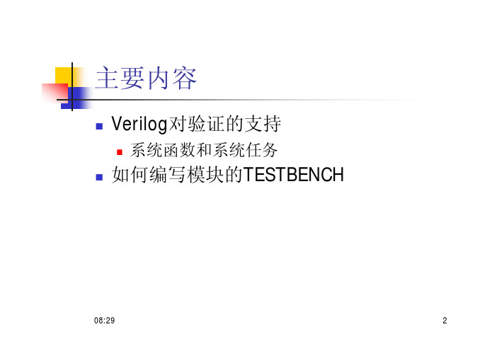
08:292主要内容Verilog 对验证的支持系统函数和系统任务如何编写模块的TESTBENCH08:293系统任务和系统函数是Verilog中预先定义好的,用于调试和编译预处理的任务或函数。
以$开头,用于控制和检测仿真模拟过程主要有:(1)用于获取仿真时间的系统函数(2)支持文本输出(检测信号、显示信号)的系统任务(3)用于文件输入、输出操作的系统任务(4)用于暂停和退出仿真的系统任务(5)用于产生随机数的系统任务08:294获取当前仿真时间的系统函数$time,$realtime,$stime:返回当前仿真时间。
$time返回一个64位的整数时间值,$realtime返回的结果是实数时间值,是更为精确的仿真时间 $stime返回一个32位整数时间值。
(对大于232的时间,返回模232的值。
使用它可以节省显示及打印空间。
)这些函数的返回值使用调用模块中`timescale 定义的模块仿真时间尺度为单位08:295例..\..\verilog_example\Dec2x4.v..\..\verilog_example\Dec_Test.v # At time 0, input is 0,0,0, output is,xxxx # At time 4, input is 0,0,0, output is,1111# At time 10, input is 0,0,1, output is,1111# At time 13, input is 0,0,1, output is,0111# At time 20, input is 1,0,1, output is,0111# At time 23, input is 1,0,1, output is,0101# At time 26, input is 1,0,1, output is,1101# At time 30, input is 1,1,1, output is,1101# At time 33, input is 1,1,1, output is,1100# At time 36, input is 1,1,1, output is,1110# At time 40, input is 0,1,1, output is,1110# At time 44, input is 0,1,1, output is,1011# At time 50, input is 0,0,1, output is,1011# At time 54, input is 0,0,1, output is,011108:296Verilog 支持的文本输出的系统任务显示任务:用于仿真模拟期间显示信息。
verilog testbench例子 -回复
verilog testbench例子-回复"Verilog Testbench Example: A Step-by-Step Guide"Introduction:In this article, we will discuss a Verilog testbench example along with a step-by-step guide. Verilog is a hardware description language (HDL) used for designing and simulating digital circuits. Testbenches play a crucial role in verifying the correctness of these designs and ensuring they meet the desired specifications. To illustrate this process, we will implement a simple 4-bit binary adder circuit and create a testbench to verify its functionality.Step 1: Designing the 4-bit Binary Adder Circuit:The first step in this process is to design the 4-bit binary adder circuit. This circuit will take two 4-bit inputs (A and B) and generate a 4-bit output (Sum). Additionally, it will have a carry output (C_out) to indicate if there is a carry generated during the addition. We will use structural modeling to create the circuit by instantiating four full-adder modules.Step 2: Implementing the Full-Adder Module:The next step is to implement the full-adder module. This module takes three inputs: A, B, and C_in, representing the bits to be added and the carry-in bit, respectively. It generates two outputs: Sum and C_out, representing the sum bit and the carry-out bit, respectively. This module can be implemented using logical gates such as XOR, AND, and OR gates.Step 3: Creating the Verilog Testbench:Once the circuit is designed and the full-adder module is implemented, we can create the Verilog testbench. The testbench is responsible for providing stimulus to the design under test (DUT) and verifying the expected outputs. It should include test vectors, monitor the DUT outputs, and compare them with the expected values.Step 4: Setting Up the Testbench:In the testbench, we need to instantiate the DUT module (the 4-bit binary adder circuit) and connect it to the inputs and outputs of thetestbench. We can also set up a clock signal that will drive the simulation. Additionally, we should define variables to store the expected output values and initialize them.Step 5: Providing Test Vectors:To test the functionality of the binary adder, we need to provide appropriate test vectors to the DUT. These test vectors represent different input combinations and their expected output values. For our example, we can create a range of test vectors that cover possible input combinations, including cases with carry propagation.Step 6: Driving the Simulation:Once the test vectors are defined, we can start the Verilog simulation. We need to drive the inputs of the DUT using the defined test vectors and provide a clock signal to synchronize the simulation. As the simulation runs, the DUT will produce outputs based on the inputs provided.Step 7: Monitoring and Assertion:During the simulation, the testbench should monitor the outputs of the DUT and compare them with the expected values stored in the variables. If any discrepancies are found, the testbench should raise an assertion and halt the simulation. This allows us to detect and debug any errors in the design.Step 8: Displaying Simulation Results:After the simulation is complete, we can display the results of the testbench. This includes information about the total simulation time, the number of test vectors executed, and the success or failure of each test vector. Additionally, we can display any error messages and debug information to guide us in identifying and fixing any issues.Conclusion:In this article, we have explored a Verilog testbench example for a 4-bit binary adder circuit. We discussed the step-by-step process of designing the circuit, implementing the full-adder module, andcreating a testbench to verify the functionality. By following this guide, you can gain a better understanding of how to create testbenches for verifying your Verilog designs. Remember to provide appropriate test vectors, monitor the DUT outputs, and assert against the expected values to ensure the correctness of your circuit.。
verilog波形仿真实例
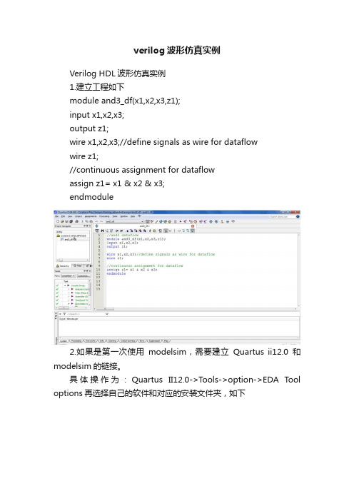
verilog波形仿真实例Verilog HDL波形仿真实例1.建立工程如下module and3_df(x1,x2,x3,z1);input x1,x2,x3;output z1;wire x1,x2,x3;//define signals as wire for dataflowwire z1;//continuous assignment for dataflowassign z1= x1 & x2 & x3;endmodule2.如果是第一次使用modelsim,需要建立Quartus ii12.0和modelsim的链接。
具体操作为:Quartus II12.0->Tools->option->EDA Tool options再选择自己的软件和对应的安装文件夹,如下3.建立测试文件(testbench)可以自己写,也可以用quartus II 自己生成(生成的只是模版,功能需要自己添加),注:testbench的输出为要测试文件的输入,即测试文件是为要测试文件产生信号用的,因此testbench的input为reg变量,输出为wire变量,具体操纵如下Processing->start->strat test bench T emplate writer然后会出现建立成功的提示,的simulation\modelsim\下面)。
4.添加信号功能如下。
`timescale 1 ns/ 1 psmodule and3_df_vlg_tst();// constants// general purpose registers//========================reg x1;//inputs are reg for test benchreg x2;reg x3;// wireswire z1;//outputs are wire for test bench//============================// assign statements (if any)and3_df i1 (// port map - connection between master ports and signals/registers .x1(x1),.x2(x2),.x3(x3),.z1(z1));initialbegin :APPlicable// code that executes only once// insert code here --> begin//===================================== ========reg [3:0] invect; //test invectfor(invect =0;invect<8;invect=invect+1)begin{x1,x2,x3} = invect [3:0];#10 $display ("x1 x2 x3 = %b ,z1 = %b",{x1,x2,x3},z1);end//===================================== =========// --> endendendmodule6.复制测试文件模块名(供下步添加test bench name用)添加测试文件。
- 1、下载文档前请自行甄别文档内容的完整性,平台不提供额外的编辑、内容补充、找答案等附加服务。
- 2、"仅部分预览"的文档,不可在线预览部分如存在完整性等问题,可反馈申请退款(可完整预览的文档不适用该条件!)。
- 3、如文档侵犯您的权益,请联系客服反馈,我们会尽快为您处理(人工客服工作时间:9:00-18:30)。
Verilog 仿真文件testbench编写样例
`timescale 1ns/100ps
module testbench;
localparam DATA_WIDTH = 32;
localparam CLK_100_PERIOD = 5;
localparam CLK_200_PERIOD = 2.5;
localparam SIM_TIME = 150000;
localparam ;
localparam ;
reg clk_100, clk_200;
wire clk;
assign clk = clk_100;
always
begin
clk_100 = 0;
forever #CLK_100_PERIOD clk_100 = ~clk_100;
end
always
begin
clk_200 = 0;
forever #CLK_200_PERIOD clk_200 = ~clk_200;
end
reg rstn;
integer fp_testin;
integer fp_matlab_out;
integer fp_sim_out;
integer fp_outdiff;
reg signed [DATA_WIDTH/2-1:0] matlab_in_re, matlab_in_im;
reg signed [DATA_WIDTH/2-1:0] matlab_out_re, matlab_out_im;
reg signed [DATA_WIDTH/2-1:0] matlab_diff_re, matlab_diff_im;
reg signed [DATA_WIDTH/2-1:0] matlab_diff_re2, matlab_diff_im2;
reg signed [DATA_WIDTH/2-1:0] max_diff_re, max_diff_im;
initial begin
max_diff_re = 0;
max_diff_im = 0;
rstn = 0;
#500
rstn = 1;
#SIM_TIME
sim_finish();
$stop();
end
task sim_finish;
begin
if(fp_testin!=0)
$fclose(fp_testin);
if(fp_matlab_out!=0)
$fclose(fp_matlab_out);
if(fp_sim_out)
$fclose(fp_sim_out);
if(fp_outdiff!=0)
$fclose(fp_outdiff);
end
endtask
initial
begin
fp_testin = 0;
fp_testin=
$fopen("txt_file/input_data.txt"," r");
if(fp_testin==0)
begin
$display("input_data.txt open failed!"); sim_finish();
$stop();
end
else begin
$fscanf(fp_testin,
"%d, %d\n",matlab_in_re,matlab_in_im); end
fp_matlab_out = 0;
fp_matlab_out =
$fopen("txt_file/matlab_out.txt"," r");
if(fp_matlab_out==0)
begin
$display("fp_matlab_out.txt open
failed!");
sim_finish();
$stop();
end
else begin
$fscanf(fp_matlab_out,"%d, %d\n",matlab _out_re,matlab_out_im);
end
fp_sim_out = 0;
fp_sim_out =
$fopen("txt_file/modelsim_out.txt",&quo t;w");
if(fp_sim_out == 0)
begin
$display("modelsim_out_re.txt open
failed!");
sim_finish();
$stop();
end
fp_outdiff = 0;
fp_outdiff =
$fopen("text_file/outdiff.txt","w& quot;);
if(fp_outdiff==0)
begin
$display("outdiff.txt open failed!"); sim_finish();
$stop();
end
end
always @(posedge clk)
begin
if(stest_wvalid && stest_wready) //ready to change
begin
if(~$feof(fp_testin))
$fscanf(fp_testin,
"%d, %d\n",matlab_in_re,matlab_in_im); end
else
begin
matlab_in_re <= matlab_in_re;
matlab_in_im <= matlab_in_im;
end
end
always @(posedge clk_100)
begin
if(mfc_wready && mfc_wvalid)
begin
matlab_diff_re <= mfc_wdata_re - matlab_out_re; matlab_diff_im <= mfc_wdata_im - matlab_out_im; matlab_diff_re2 <= matlab_out_re - mfc_wdata_re ; matlab_diff_im2 <= matlab_out_im - mfc_wdata_im ; if(max_diff_re < matlab_diff_re)
begin
max_diff_re <= matlab_diff_re;
$display("max_diff_re:%d
max_diff_im:%d\n",max_diff_re,max_diff_im); end
else if(max_diff_re < matlab_diff_re2)
begin
max_diff_re <= matlab_diff_re2;
$display("max_diff_re:%d
max_diff_im:%d\n",max_diff_re,max_diff_im); end
if(max_diff_im < matlab_diff_im)
begin
max_diff_im <= matlab_diff_im;
$display("max_diff_re:%d
max_diff_im:%d\n",max_diff_re,max_diff_im); end
else if(max_diff_im < matlab_diff_im2)
begin
max_diff_im <= matlab_diff_im2;
$display("max_diff_re:%d
max_diff_im:%d\n",max_diff_re,max_diff_im); end
$fscanf(fp_matlab_out,"%d, %d\n",matlab _out_re,matlab_out_im);
$fwrite(fp_sim_out, "%d, %d\n",
mfc_wdata_re,mfc_wdata_im);
$fwrite(fp_outdiff,
"%d, %d\n",matlab_diff_re,matlab_diff_i m);
end
end
endmodule。