OB3393SCPA规格书 Datasheet
MCZ33937AEK;MCZ33937AEKR2;MCZ33937EK;MCZ33937EKR2;中文规格书,Datasheet资料
Figure 3. 33937A Pin Connections Table 1. 33937A Pin Definitions A functional description of each pin can be found in the Functional Pin Description section beginning on page 20.
Freescale Semiconductor Advance Information
Document Number: MC33937 Rev. 8.0, 8/2012
Three Phase Field Effect Transistor Pre-driver
The 33937A is a field effect transistor (FET) pre-drivers designed for three phase motor control and similar applications. The integrated circuit (IC) uses SMARTMOS technology. The IC contains three high side FET pre-drivers and three low side FET pre-drivers. Three external bootstrap capacitors provide gate charge to the high side FETs. The IC interfaces to a MCU via six direct input control signals, an SPI port for device setup and asynchronous reset, enable and interrupt signals. Both 5.0 and 3.0 V logic level inputs are accepted and 5.0 V logic level outputs are provided. Features • Fully specified from 8.0 to 40 V covers 12 and 24 V automotive systems • Extended operating range from 6.0 to 58 V covers 12 and 42 V systems • Greater than 1.0 A gate drive capability with protection • Protection against reverse charge injection from CGD and CGS of external FETs • Includes a charge pump to support full FET drive at low battery voltages • Dead time is programmable via the SPI port • Simultaneous output capability enabled via safe SPI command
ob6683cgpa规格书

ob6683cgpa规格书英文回答:OB6683CGPA Specification.Introduction:The OB6683CGPA specification outlines the requirements and standards for the OB6683CGPA product. Thisspecification aims to provide a detailed description of the product's features, functionality, and performance expectations. In this response, I will discuss the key aspects of the OB6683CGPA specification and provide examples to illustrate its application.Product Features:The OB6683CGPA is a versatile and high-performance device that offers a range of features to meet the needs of users. It is equipped with advanced technology andinnovative design elements. Some of its notable features include:1. High-resolution display: The OB6683CGPA boasts a vibrant and sharp display, allowing users to enjoy crystal-clear visuals and an immersive viewing experience.2. Powerful processor: With a state-of-the-art processor, the OB6683CGPA delivers lightning-fast performance, enabling seamless multitasking and smooth operation of resource-intensive applications.3. Extensive storage capacity: The OB6683CGPA offers ample storage space, allowing users to store a large amount of data, including photos, videos, and documents, without worrying about running out of space.4. Advanced camera system: The OB6683CGPA is equipped with a high-quality camera system, enabling users to capture stunning photos and videos with exceptional clarity and detail.Performance Expectations:The OB6683CGPA is designed to deliver exceptional performance across various tasks and applications. Its powerful hardware and optimized software ensure smooth and efficient operation. Some performance expectations for the OB6683CGPA include:1. Fast and responsive user interface: The OB6683CGPA provides a seamless user experience with its quick and responsive interface. Users can navigate through menus, open applications, and perform tasks without any lag or delay.2. Smooth gaming experience: The OB6683CGPA is capable of handling graphically demanding games with ease. Users can enjoy a smooth and immersive gaming experience without experiencing any frame drops or stuttering.3. Efficient multitasking: The OB6683CGPA allows users to run multiple applications simultaneously without compromising performance. Users can switch between appsseamlessly and enjoy a seamless multitasking experience.4. Long battery life: The OB6683CGPA is equipped with a high-capacity battery that provides extended usage time. Users can enjoy using the device for extended periodswithout worrying about frequent recharging.中文回答:OB6683CGPA规格书。
OB3Z12A规格书

Product ListOB3Z12ADescriptionThe OB3Z12A is a LED lighting controller. It has hardware dimming mechanism supporting up to 3-channel dimming control. The control interfaces include Liner DC, VR, Key/Button, PWM duty and IR, various digital and analog diming control methods. The OB3Z12A equips with serial communication interfaces for inter-connection to host or remote controllers. The on-chip non-volatile memory contains the system preset parameters and configurations.Features●Operating V oltage: 4.5V ~ 5.5V●3-ch PWM dimming control output● 1 analog VR dimming control input● 1 analog DC-in dimming control input● 1 digital PWM duty dimming control input● 1 digital IR remote dimming control input●Serial interfaces: UART, I2C.●Package type: 8-SOP.Pin Configuration8-SOPPin DescriptionPin Symbol I/O Description1 RX/AN0 I VR, analog diming control input. Serial Receiver Input2 TX/AN1 I/O Liner analog diming control input. Serial Transmitter Output3 DIM3 O PWM dimming output ch-34 DIM2 O PWM dimming output ch-25 VSS I Power supply6 SDA/IR I/O I2C Data. IR input7 DIM1/SCL/Duty I/O I2C Clock. PWM dimming output ch-1. Duty dimming control input8 VDD I Power SupplyOperating ConditionsSymbol Description Min. Typ. Max. Unit. RemarksTA Operating temperature -40 25 85 ℃Ambient temperature under bias VDD Supply voltage 4.5 5.5 VDC CharacteristicsT A = -40℃ to 85℃, V dd= 5.0VSymbol Parameter Valid Min Max Units ConditionsVIL1Input Low-voltage DIMx,SDA,SCL,Tx,Rx-0.5 0.8 V Vdd=5VVIH1Input High-voltage DIMx,SDA,SCL,Tx,Rx2.0 V CC + 0.5 VVOL Output Low-voltage DIMx,SDA,SCL,Tx,Rx0.4 V IOL=4.9mAVOH1Output High-voltageusing Strong Pull-upDIMx,SDA,SCL,Tx,Rx90% V CC V IOH= -4.6mA2.4 V IOH= -14mAVOH2Output High-voltageusing Weak Pull-upDIMx,SDA,SCL,Tx,Rx2.4 V IOH= -250uAIIL Logic 0 Input Current DIMx,SDA,SCL,Tx,Rx-75 uA Vin= 0.45VITL Logical TransitionCurrentDIMx,SDA,SCL,Tx,Rx-650 uA Vin= 2.0VILI Input Leakage Current DIMx,SDA,SCL,Tx,Rx±10 uA 0.45V<Vin<VccICC Power Supply Current VDD 5 mA Vdd =5V 25 ℃。
OB3398 Datasheet_铱宝_150602
O
nB
On chip Over temperature Section T_otp T_otp_rec 135 120 ℃ ℃
Note:
1. Freq_Max indicates IC internal maximum clock frequency. In system application, the maximum operation frequency of 103KHz nominal occurs at maximum output power or the transition point from CV to CC.
tia
Ordering Information Part Number Description OB3398MP SOT23-5, Pb-free,T&R
ratings” may cause permanent damage to the device. These are stress ratings only, functional operation of the device at these or any other conditions beyond those indicated under “recommended operating conditions” is not implied. Exposure to absolute maximum-rated conditions for extended periods may affect device reliability.
V_clamping T_r T_f
Output clamp voltage Output rising time 1V~ 9V@ CL=500pF Output falling time 9V~1V@ CL=500pF Over temperature protection trigger point Over temperature protection recovery point
欧姆伯特电子 3R3型号电感说明书

Dimensions: [mm]Scale - 5:1Product Marking:Marking3R3 (Inductance Code)7440404203374404042033BC74404042033T e m p e r a t u r eT pT L74404042033Cautions and Warnings:The following conditions apply to all goods within the product series of WE-LQS of Würth Elektronik eiSos GmbH & Co. KG:General:•This electronic component is designed and manufactured for use in general electronic equipment.•Würth Elektronik must be asked for written approval (following the PPAP procedure) before incorporating the components into any equipment in fields such as military, aerospace, aviation, nuclear control, submarine, transportation (automotive control, train control, ship control), transportation signal, disaster prevention, medical, public information network etc. where higher safety and reliability are especially required and/or if there is the possibility of direct damage or human injury.•Electronic components that will be used in safety-critical or high-reliability applications, should be pre-evaluated by the customer. •The component is designed and manufactured to be used within the datasheet specified values. If the usage and operation conditions specified in the datasheet are not met, the wire insulation may be damaged or dissolved.•Do not drop or impact the components, the component may be damaged.•Würth Elektronik products are qualified according to international standards, which are listed in each product reliability report. Würth Elektronik does not warrant any customer qualified product characteristics beyond Würth Elektroniks’ specifications, for its validity and sustainability over time.•The responsibility for the applicability of the customer specific products and use in a particular customer design is always within the authority of the customer. All technical specifications for standard products also apply to customer specific products.Product specific:Soldering:•The solder profile must comply with the technical product specifications. All other profiles will void the warranty.•All other soldering methods are at the customers’ own risk.•Strong forces which may affect the coplanarity of the components’ electrical connection with the PCB (i.e. pins), can damage the part, resulting in avoid of the warranty.Cleaning and Washing:•Washing agents used during the production to clean the customer application might damage or change the characteristics of the wire insulation, marking or plating. Washing agents may have a negative effect on the long-term functionality of the product.•Using a brush during the cleaning process may break the wire due to its small diameter. Therefore, we do not recommend using a brush during the PCB cleaning process.Potting:•If the product is potted in the customer application, the potting material may shrink or expand during and after hardening. Shrinking could lead to an incomplete seal, allowing contaminants into the core. Expansion could damage the components. We recommend a manual inspection after potting to avoid these effects.Storage Conditions:• A storage of Würth Elektronik products for longer than 12 months is not recommended. Within other effects, the terminals may suffer degradation, resulting in bad solderability. Therefore, all products shall be used within the period of 12 months based on the day of shipment.•Do not expose the components to direct sunlight.•The storage conditions in the original packaging are defined according to DIN EN 61760-2.•The storage conditions stated in the original packaging apply to the storage time and not to the transportation time of the components. Packaging:•The packaging specifications apply only to purchase orders comprising whole packaging units. If the ordered quantity exceeds or is lower than the specified packaging unit, packaging in accordance with the packaging specifications cannot be ensured. Handling:•Violation of the technical product specifications such as exceeding the nominal rated current will void the warranty.•Applying currents with audio-frequency signals may result in audible noise due to the magnetostrictive material properties.•The temperature rise of the component must be taken into consideration. The operating temperature is comprised of ambient temperature and temperature rise of the component.The operating temperature of the component shall not exceed the maximum temperature specified.These cautions and warnings comply with the state of the scientific and technical knowledge and are believed to be accurate and reliable.However, no responsibility is assumed for inaccuracies or incompleteness.Würth Elektronik eiSos GmbH & Co. KGEMC & Inductive SolutionsMax-Eyth-Str. 174638 WaldenburgGermanyCHECKED REVISION DATE (YYYY-MM-DD)GENERAL TOLERANCE PROJECTIONMETHODChriB001.0072023-02-28DIN ISO 2768-1mDESCRIPTIONWE-LQS SMT Semi-ShieldedPower Inductor ORDER CODE74404042033SIZE/TYPE BUSINESS UNIT STATUS PAGEImportant NotesThe following conditions apply to all goods within the product range of Würth Elektronik eiSos GmbH & Co. KG:1. General Customer ResponsibilitySome goods within the product range of Würth Elektronik eiSos GmbH & Co. KG contain statements regarding general suitability for certain application areas. These statements about suitability are based on our knowledge and experience of typical requirements concerning the areas, serve as general guidance and cannot be estimated as binding statements about the suitability for a customer application. The responsibility for the applicability and use in a particular customer design is always solely within the authority of the customer. Due to this fact it is up to the customer to evaluate, where appropriate to investigate and decide whether the device with the specific product characteristics described in the product specification is valid and suitable for the respective customer application or not.2. Customer Responsibility related to Specific, in particular Safety-Relevant ApplicationsIt has to be clearly pointed out that the possibility of a malfunction of electronic components or failure before the end of the usual lifetime cannot be completely eliminated in the current state of the art, even if the products are operated within the range of the specifications.In certain customer applications requiring a very high level of safety and especially in customer applications in which the malfunction or failure of an electronic component could endanger human life or health it must be ensured by most advanced technological aid of suitable design of the customer application that no injury or damage is caused to third parties in the event of malfunction or failure of an electronic component. Therefore, customer is cautioned to verify that data sheets are current before placing orders. The current data sheets can be downloaded at .3. Best Care and AttentionAny product-specific notes, cautions and warnings must be strictly observed. Any disregard will result in the loss of warranty.4. Customer Support for Product SpecificationsSome products within the product range may contain substances which are subject to restrictions in certain jurisdictions in order to serve specific technical requirements. Necessary information is available on request. In this case the field sales engineer or the internal sales person in charge should be contacted who will be happy to support in this matter.5. Product R&DDue to constant product improvement product specifications may change from time to time. As a standard reporting procedure of the Product Change Notification (PCN) according to the JEDEC-Standard inform about minor and major changes. In case of further queries regarding the PCN, the field sales engineer or the internal sales person in charge should be contacted. The basic responsibility of the customer as per Section 1 and 2 remains unaffected.6. Product Life CycleDue to technical progress and economical evaluation we also reserve the right to discontinue production and delivery of products. As a standard reporting procedure of the Product Termination Notification (PTN) according to the JEDEC-Standard we will inform at an early stage about inevitable product discontinuance. According to this we cannot guarantee that all products within our product range will always be available. Therefore it needs to be verified with the field sales engineer or the internal sales person in charge about the current product availability expectancy before or when the product for application design-in disposal is considered. The approach named above does not apply in the case of individual agreements deviating from the foregoing for customer-specific products.7. Property RightsAll the rights for contractual products produced by Würth Elektronik eiSos GmbH & Co. KG on the basis of ideas, development contracts as well as models or templates that are subject to copyright, patent or commercial protection supplied to the customer will remain with Würth Elektronik eiSos GmbH & Co. KG. Würth Elektronik eiSos GmbH & Co. KG does not warrant or represent that any license, either expressed or implied, is granted under any patent right, copyright, mask work right, or other intellectual property right relating to any combination, application, or process in which Würth Elektronik eiSos GmbH & Co. KG components or services are used.8. General Terms and ConditionsUnless otherwise agreed in individual contracts, all orders are subject to the current version of the “General Terms and Conditions of Würth Elektronik eiSos Group”, last version available at .Würth Elektronik eiSos GmbH & Co. KGEMC & Inductive SolutionsMax-Eyth-Str. 174638 WaldenburgGermanyCHECKED REVISION DATE (YYYY-MM-DD)GENERAL TOLERANCE PROJECTIONMETHODChriB001.0072023-02-28DIN ISO 2768-1mDESCRIPTIONWE-LQS SMT Semi-ShieldedPower Inductor ORDER CODE74404042033SIZE/TYPE BUSINESS UNIT STATUS PAGE。
DC339-A -B低压差稳压器数据手册说明书

12REFERENCEDESIGNATOR QUANTITY PART NUMBER DESCRIPTION VENDOR TELEPHONE ADJ10Optional ResistorC110603ZG105ZAT1A1µF 10V Y5V Chip Capacitor AVX(843) 946-0362 C210402ZG104ZAT1A0.1µF 10V Y5V Chip Capacitor AVX(843) 946-0362 C31LMK325BJ106MN10µF 10V X7R Chip Capacitor Taiyo-Yuden(408) 573-4150 E1 to E442308-2Pad Turret Mill-Max(516) 922-6000 JP10Optional JumperJP216351-12G1Connector, SMT2X6, 0.39" Gap Comm-Con(626) 301-4200 Shunts for2CTAIJ1MM-G Shunts for 0.39" Gap Comm-Con(626) 301-4200 JP1 and JP2R11CR05-2613FM261k 1/16W 1% Chip Resistor AAC(800) 508-1521 R21CR05-3653FM365k 1/16W 1% Chip Resistor AAC(800) 508-1521 R31CR05-4223FM422k 1/16W 1% Chip Resistor AAC(800) 508-1521 R41CR05-7683FM768k 1/16W 1% Chip Resistor AAC(714) 255-9186 R51CR05-2493FM249k 1/16W 1% Chip Resistor AAC(714) 255-9186 U11LT1762EMS8 or8-Lead MSOP IC Version -A LTC(408) 432-1900 LT1962EMS88-Lead MSOP IC Version -BPARTS LISTOPERATIOUHOOK-UPSolid turret terminals are provided for easy connection to supplies and test equipment. Connect a 0V to 20V, 0.5A power supply across the IN and GND terminals and the load across the OUT and GND terminals. The SHDN pin can be disconnected from IN via JP1 to allow for separate shutdown control via a secondary control line. JP2 can be used to select any of a number of common fixed output voltages, or used in conjunction with ADJ1 to create a custom output voltage using the formula:ADJ1 = (V OUT – 1.22V)/4.93µAOUTPUT CAPACITOR SELECTIONThe output capacitor C3 is a 10µF X7R ceramic chip capacitor. Should a different output capacitor be desired, care must be exercised with the selection. Many ceramic capacitor dielectrics exhibit strong temperature and voltage characteristics that reduce their effective capaci-tance to as low as 10% to 20% of nominal over the full range. For further information, see Linear Technology Application Note 83, “Performance Verification of Low Noise, Low Dropout Regulators,” Appendix␣B, “Capaci-tor Selection Considerations,” reprinted below.CAPACITOR SELECTION CONSIDERATIONSBypass Capacitance and Low Noise Performance Adding a capacitor between the regulator’s V OUT and BYP pins lowers output noise. A good quality, low leakage capacitor is recommended. This capacitor bypasses the regulator’s reference, providing a low frequency noise pole. A 0.01µF capacitor lowers the output voltage noise to 20µV RMS. Using a bypass capacitor also improves transient response. With no bypassing and a 10µF output capacitor, a 10mA to 500mA load step settles within 1% of final value in under 100µs. With a 0.01µF bypass capacitor, the output settles within 1% for the same load step in under 10µs; total output deviation is inside 2.5%. Regulator start-up time is inversely proportional to bypass capacitor size, slowing to 15ms with a 0.01µF bypass capacitor and 10µF at the output.34567Information furnished by Linear Technology Corporation is believed to be accurate and reliable.However, no responsibility is assumed for its use. Linear Technology Corporation makes no represen-tation that the interconnection of its circuits as described herein will not infringe on existing patent rights.8dc339 LT/TP 0301 500 • PRINTED IN USA© LINEAR TECHNOLOGY CORPORA TION 2001Linear Technology Corporation1630 McCarthy Blvd., Milpitas, CA 95035-7417(408) 432-1900 q FAX: (408) 434-0507 q 。
OB3392 Datasheet
o
富
260 ℃
Absolute Maximum Ratings Parameter VDD Voltage GATE Voltage CS Input Voltage FB Input Voltage CMP Input Voltage Min/Max Operating Junction Temperature TJ Min/Max Storage Temperature Tstg Lead Temperature (Soldering, 10secs)
Value -0.3 to 35V -0.3 to 10V -0.3 to 7V -0.3 to 7V -0.3 to 7V
-55 to 150 ℃
Preliminary Datasheet OB_DOC_DS_339200
华
-40 to 150 ℃
OB3392
High PF, High Precision Offline LED Lighting Controller
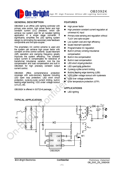
TYPICAL APPLICATION
O
n-
©On-Bright Electronics
Br ig
ht
co
nf
id
Confidential -1-
en t
LED lighting
APPLICATIONS
ia
lt
o
富
Preliminary Datasheet OB_DOC_DS_339200
华
OB3392
ELECTRICAL CHARACTERISTICS
(TA = 25℃, VDD=15V, if not otherwise noted) Symbol Parameter Supply Voltage (VDD) Section I start-up I op UVLO(OFF) UVLO(ON) VDD_OVP TLEB Vth_ocp Vout_ovp Start-up Current Operation Current VDD Under Voltage Lockout Exit VDD Under Voltage Lockout Enter VDD Over Voltage Protection LEB Time Over Current Threshold Output Over Voltage Protection 19 8 27 VDD=20V 1 1.3 21 9 30 3 2.0 23 uA mA Test Conditions Min Typ Max Unit
OB3Z12A规格书
Product ListOB3Z12ADescriptionThe OB3Z12A is a LED lighting controller. It has hardware dimming mechanism supporting up to 3-channel dimming control. The control interfaces include Liner DC, VR, Key/Button, PWM duty and IR, various digital and analog diming control methods. The OB3Z12A equips with serial communication interfaces for inter-connection to host or remote controllers. The on-chip non-volatile memory contains the system preset parameters and configurations.Features●Operating V oltage: 4.5V ~ 5.5V●3-ch PWM dimming control output● 1 analog VR dimming control input● 1 analog DC-in dimming control input● 1 digital PWM duty dimming control input● 1 digital IR remote dimming control input●Serial interfaces: UART, I2C.●Package type: 8-SOP.Pin Configuration8-SOPPin DescriptionPin Symbol I/O Description1 RX/AN0 I VR, analog diming control input. Serial Receiver Input2 TX/AN1 I/O Liner analog diming control input. Serial Transmitter Output3 DIM3 O PWM dimming output ch-34 DIM2 O PWM dimming output ch-25 VSS I Power supply6 SDA/IR I/O I2C Data. IR input7 DIM1/SCL/Duty I/O I2C Clock. PWM dimming output ch-1. Duty dimming control input8 VDD I Power SupplyOperating ConditionsSymbol Description Min. Typ. Max. Unit. RemarksTA Operating temperature -40 25 85 ℃Ambient temperature under bias VDD Supply voltage 4.5 5.5 VDC CharacteristicsT A = -40℃ to 85℃, V dd= 5.0VSymbol Parameter Valid Min Max Units ConditionsVIL1Input Low-voltage DIMx,SDA,SCL,Tx,Rx-0.5 0.8 V Vdd=5VVIH1Input High-voltage DIMx,SDA,SCL,Tx,Rx2.0 V CC + 0.5 VVOL Output Low-voltage DIMx,SDA,SCL,Tx,Rx0.4 V IOL=4.9mAVOH1Output High-voltageusing Strong Pull-upDIMx,SDA,SCL,Tx,Rx90% V CC V IOH= -4.6mA2.4 V IOH= -14mAVOH2Output High-voltageusing Weak Pull-upDIMx,SDA,SCL,Tx,Rx2.4 V IOH= -250uAIIL Logic 0 Input Current DIMx,SDA,SCL,Tx,Rx-75 uA Vin= 0.45VITL Logical TransitionCurrentDIMx,SDA,SCL,Tx,Rx-650 uA Vin= 2.0VILI Input Leakage Current DIMx,SDA,SCL,Tx,Rx±10 uA 0.45V<Vin<VccICC Power Supply Current VDD 5 mA Vdd =5V 25 ℃。
OB6663L Datasheet

FEATURES
■
■ ■ ■ ■ ■ ■ ■ ■ ■ ■ ■ ■ ■ ■
on
ht C
O
nBr
©On-Bright Electronics
ig
fid en tia
Integrated Transition Mode (TM) PFC Controller and Quasi-Resonant (QR) PWM Controller Built-in Dual Output PFC Control Multi-Mode Operation for QR Stage Separated AGND and PGND Provide Better Noise Immunity Analog Multiplier with Built-in THD Optimizer for PFC Stage Line Feed-forward Compensation for PFC Stage Enhanced Dynamic Response for PFC Stage Less than 200mW Standby Power Consumption Minimum QR Short Circuit Power Consumption Audio Noise Free Operation External Latch Triggering for Both Converters Minimum OFF time for Ringing Suppression Maximum ON Time Limit for QR Converter Built-in 4ms Soft Start for QR Converter Internal Leading Edge Blanking for Both Converters
CV3393BL-G-20_Specification_V1.0规格书
FORM-70-016-01LED TV CONTROL BOARD SPECIFICATIONMODEL : CV3393BL-G-20Approved by CultraviewApproved by CustomerAUTHOR : WP .WU Comments :CHECKED BY : CHECKED BY :APPROVED BY :APPROVED BY:DATE:2015.06.26DATE:Company’s seal:Please return us one original approved by you with your signatures. 客户承认签章后敬请寄回正本一份C UL T RA V I EWITEM1. CHANGE THE LIST OF UPGRADES (2)2. GENERAL DESCRIPTION (3)3. FEATURES (4)4. PRESET MODE FOR USB (5)5. ENVIRONMENTAL CONDITION (7)6. SUBSTITUTABLE PRIMARY MATERIALS (8)7. PICTURE (10)8. INTERFACE DEFINITION (11)9. CONFIGURATION (13)10. APPLICATION REQUIREMENT (14)11. EXCURSUS (15)1. CHANGE THE LIST OF UPGRADESVersion Description Page redactionChecked DateV1.0 First Release ALL WP .WUJun.26, 2015C UL T RA V I EW2. GENERAL DESCRIPTIONThis product is digital & analogue TV board, can receive the NTSC analogue television and the ATSC digital television. Apply to the North American ATSC high-definition TV market.TV supports ATSC (meet the performance requirements of A74), NTSC, ClearQAM (meet the performance requirements of ITU-J83).Supports USB 2.0 Multimedia Player;supports audio and video play; supportspicture browse.Supports USB update.Analogue and digital HD port input signal largest support 1080PThe largest support various TFT-LCD 1920x1080 resolutions module. HDMI 1.3/1.4 Compliant; HDCP 1.2 Compliant. Supports MHL; Supports ARC.3-D video decoding and Chroma separation3-D motion adaptive video de-interlacers with edge-oriented adaptive algorithmfor smooth low-angle edges 3-D video noise reductionSupports Closed Caption (analog CC 608/ analog CC 708/digital CC 608/ digitalCC 708),V-chip and SCTE.Supports BTSC/A2/EIA-J demodulationSupports digital audio format decoding:MPEG-1,MPEG2-2(Layer I/II),DolbyDigital(AC-3) Automatic 3:2 pull-down & 2:2 pull-down detection and recoveryMStar 5rd Generation Advanced Color Engine (MStarACE-5) automatic pictureenhancementReliable EMC and ESD handleC UL T RA V I EW3. FEATURESPANELType TFT-LCDResolution Max. 1920X1080 Interface Single/ Double LVDS ATVInput Impedance 75Ω Video System NTSCSound SystemM, J, 4.43.BTSC/A2DTVInput Impedance 75ΩBandwidth 6MHz Modulation ATSC:8VSB QAM:64QAM, 256QAM Video System MPEG 2 MP@HL Sound System MPEG 1/ layer 1/AC-3 PCSync H: 30-75KHz V: 56-75Hz Video Level 0.7Vp-p@75ohm MODE Max 1920X1080@60Hz AVColor system PAL/NTSC/SECAM Video Level 1Vp-p@75ohm Audio Level 500mV rmsYPbPrVideo LevelY:1Vp-p@75ohm,PbPr:0.7Vp-p@75ohm Audio Level 500mVrmsFormat480i, 480p, 576i, 576p, 720p, 1080i, 1080pHDMIVideo Level Standard TMDSFormat480i, 480p, 576i, 576p, 720p, 1080i, 1080pKeyboardPower/Menu/Source/ Up/ Down/ Left/ RightOSD Language English/ French/ Spanish Audio Amplifier 2 X3W @ 4ohm THD<10% Power input DC +12VStandby< 0.3W(Main Board Only)C UL T RA V I EW4. PRESET MODE FOR USBUSB FORMAT MODEMediaFile Exit. Codec RemarkVideoAudio .aviXvid,MPEG-2,MPEG-4,H.264,(Divx Need license) MP3 WMA AAC MP2 PCM(AC3 Need license) (DTS Need license) The Max Resolution And FrameRate:1080p@30fps Max Data Rate: 20 Mbps.mp4 MPEG-2,MPEG-4,H.264(Divx Need license) .mpgMPEG-1,MPEG-2 .mkv / .mov MPEG-1/2/4,H.264, (Divx Need license) .datMPEG-1MP2(AC3 Need license) (DTS Need license)The MaxResolution:352×288 Max Data Rate: 20 Mbps .vob MPEG-2The MaxResolution:720×576 Max Data Rate: 20 Mbps .rm/ .rmvbRV8,RV9, RV10COOKThe Max Resolution And FrameRate:1080p@30fpsMax Data Rate: 10 MbpsPHOTO .jpgProgressive JPEG Max Resolution: 1024×768 .jpegBaseline JPEGMax Resolution: 15360×8640 .bmg---- Max Resolution: 9600×6400 Pixel Depth:1/4/8/16/24/32 bpp.png Non-Interlaced Max Resolution: 9600×6400 InterlacedMax Resolution: 1200×800MUSIC.mp3--- MP3Sample Rate: 32K~48KHzBit Rate: 32K~320Kbps Channel: Mono/Stereo.wma --- WMA.m4a / .aac---AACSample Rate: 8K~48KHz Bit Rate: 24K~384KbpsC UL T RA V I EWChannel: Mono/StereoTEXT .txt ANSI/UNICODE GB/UTF8 File Size:Max 1MBNote :1)This product includes the following optional patented technologies : Dolby, DTS, DIVX, SRS , etc. If you need to use these patented, please provide the patent license to us, so that the product can meet your requirements . (此产品包括如下可选的专利技术:DOLBY 、DTS 、DIVX 、SRS 等,如您需要开通这些功能,请提前提供相关专利许可给到我司,以便产品能满足您的要求。
LM339_datasheet

2
LM339, LM239, LM2901, LM2901V, NCV2901, MC3302
ELECTRICAL CHARACTERISTICS (VCC = +5.0 Vdc, TA = +25°C, unless otherwise noted)
−
±5.0 ±50
−
±5.0 ±50
−
±3.0 ±100 nA
0
−
VCC
0
−
VCC
0
−
VCC
V
−1.5
−1.5
−1.5
Supply Current RL = ∞ (For All Comparators) RL = ∞, VCC = 30 Vdc
Voltage Gain RL ≥ 15 kW, VCC = 15 Vdc
LM339, LM239, LM2901, LM2901V, NCV2901, MC3302
Single Supply Quad Comparators
These comparators are designed for use in level detection, low−level sensing and memory applications in consumer, automotive, and industrial electronic applications.
14 Output 3 13 Output 4 12 GND ) 11 + Input 4 4 * 10 − Input 4 ) 9 + Input 3 3* 8 − Input 3
(Top View)
MAXIM MAX338 MAX339 数据手册

The MAX338/MAX339 are monolithic, CMOS analog multiplexers (muxes). The 8-channel MAX338 is designed to connect one of eight inputs to a common output by control of a 3-bit binary address. The dual, 4-channel MAX339 is designed to connect one of four inputs to a common output by control of a 2-bit binary address. Both devices can be used as either a mux or a demux. On-resistance is 400Ωmax, and the devices conduct current equally well in both directions.These muxes feature extremely low off leakages (less than 20pA at +25°C), and extremely low on-channel leakages (less than 50pA at +25°C). The new design offers guaranteed low charge injection (1.5pC typ) and electrostatic discharge (ESD) protection greater than 2000V, per method 3015.7. These improved muxes are pin-compatible upgrades for the industry-standard DG508A and DG509A. For similar Maxim devices with lower leakage and charge injection but higher on-resis-tance, see the MAX328 and MAX329.The MAX338/MAX339 operate from a single +4.5V to +30V supply or from dual supplies of ±4.5V to ±20V.All control inputs (whether address or enable) are TTL compatible (+0.8V to +2.4V) over the full specified tem-perature range and over the ±4.5V to ±18V supply range. These parts are fabricated with Maxim’s 44V sili-con-gate process.________________________ApplicationsData-Acquisition Systems Sample-and-Hold Circuits Test Equipment Heads-Up Displays Military RadiosCommunications Systems Guidance and Control SystemsPBX, PABX____________________________Features♦On-Resistance, <400Ωmax ♦Transition Time, <500ns ♦On-Resistance Match, <10Ω♦NO-Off Leakage Current, <20pA at +25°C ♦1.5pC Charge Injection♦Single-Supply Operation (+4.5V to +30V)Bipolar-Supply Operation (±4.5V to ±20V)♦Plug-In Upgrade for Industry-Standard DG508A/DG509A ♦Rail-to-Rail Signal Handling ♦TTL/CMOS-Logic Compatible♦ESD Protection >2000V, per Method 3015.7Ordering InformationMAX338/MAX3398-Channel/Dual 4-Channel,Low-Leakage, CMOS Analog Multiplexers________________________________________________________________Maxim Integrated Products 1_____________________Pin Configurations/Functional Diagrams/Truth Tables19-0272; Rev 3; 11/04Ordering Information continued at end of data sheet.*Contact factory for dice specifications.**Contact factory for availability.For pricing, delivery, and ordering information,please contact Maxim/Dallas Direct!at 1-888-629-4642, or visit Maxim’s website at .General DescriptionM A X 338/M A X 3398-Channel/Dual 4-Channel,Low-Leakage, CMOS Analog Multiplexers 2_______________________________________________________________________________________ABSOLUTE MAXIMUM RATINGSELECTRICAL CHARACTERISTICS—Dual Supplies(V+ = +15V, V- = -15V, GND = 0V, V AH = +2.4V, V AL = +0.8V, T A = T MIN to T MAX , unless otherwise noted.)Stresses beyond those listed under “Absolute Maximum Ratings” may cause permanent damage to the device. These are stress ratings only, and functional operation of the device at these or any other conditions beyond those indicated in the operational sections of the specifications is not implied. Exposure to absolute maximum rating conditions for extended periods may affect device reliability.Voltage Referenced to V-V+............................................................................-0.3V, 44V GND.........................................................................-0.3V, 25V Digital Inputs, NO, COM (Note 1)...........(V- - 2V) to (V+ + 2V) or30mA (whichever occurs first)Continuous Current (any terminal)......................................30mA Peak Current, NO or COM(pulsed at 1ms, 10% duty cycle max)..........................100mAContinuous Power Dissipation (TA = +70°C)Plastic DIP (derate 10.53mW/°C above +70°C)..........842mW Narrow SO (derate 8.70mW/°C above +70°C)............696mW 16-Pin TQFN (derate 21.3mW/°C above +70°C).......1702mW CERDIP (derate 10.00mW/°C above +70°C)...............800mW Operating Temperature RangesMAX33_C__........................................................0°C to +70°C MAX33_E__......................................................-40°C to +85°C MAX33_MJE ..................................................-55°C to +125°C Storage Temperature Range.............................-65°C to +150°C Lead Temperature (soldering, 10sec).............................+300°CNote 1:Signals on NO, COM, EN, A0, A1, or A2 exceeding V+ or V- are clamped by internal diodes. Limit forward current to maximum current ratings.MAX338/MAX3398-Channel/Dual 4-Channel,Low-Leakage, CMOS Analog Multiplexers_______________________________________________________________________________________3ELECTRICAL CHARACTERISTICS—Dual Supplies (continued)(V+ = +15V, V- = -15V, GND = 0V, V AH = +2.4V, V AL = +0.8V, T A = T MIN to T MAX , unless otherwise noted.)M A X 338/M A X 3398-Channel/Dual 4-Channel,Low-Leakage, CMOS Analog Multiplexers 4_______________________________________________________________________________________ELECTRICAL CHARACTERISTICS—Single Supply(V+ = +12V, V- = 0V, GND = 0V, V AH = +2.4V, V AL = +0.8V, T A = T MIN to T MAX , unless otherwise noted.)Note 2:The algebraic convention where the most negative value is a minimum and the most positive value a maximum is used inthis data sheet.Note 3:Guaranteed by design.Note 4:ΔR ON = R ON(MAX)- R ON(MIN).Note 5:Leakage parameters are 100% tested at the maximum rated hot temperature and guaranteed by correlation at +25°C.Note 6:Worst-case isolation is on channel 4 because of its proximity to the drain pin. Off isolation = 20log V COM /V NO , whereV COM = output and V NO = input to off switch.MAX338/MAX3398-Channel/Dual 4-Channel,Low-Leakage, CMOS Analog Multiplexers_______________________________________________________________________________________5600ON-RESISTANCE vs. V COM(DUAL SUPPLIES)500010*******-2020-1515-1010-55400V COM (V)R O N (Ω)ON-RESISTANCE vs. V COM OVER TEMPERATURE (DUAL SUPPLIES)100200300-1515-1010-550400V COM (V)R O N (Ω)12001400ON-RESISTANCE vs. V COM(SINGLE SUPPLY)100002004006001520105800V COM (V)R O N (Ω)600700ON-RESISTANCE vs. V COM OVER TEMPERATURE (SINGLE SUPPLY)500010020030015105400V COM (V)R O N (Ω)30CHARGE INJECTION vs. V COM200-30-20-100-1515-1010-55010V COM (V)Q j (p C )40100.0001-55125OFF LEAKAGE vs. TEMPERATURE1TEMPERATURE (°C)O F F L E A K A G E (n A )250.010.001-35-15650.1100100045851055100.0001-55125ON LEAKAGE vs. TEMPERATURE1TEMPERATURE (°C)O N L E A K A G E (n A )250.010.001-35-15650.11001000458510551000.001-55125SUPPLY CURRENT vs. TEMPERATURE10TEMPERATURE (°C)I +, I - (μA )250.10.01-35-156514585105510006001000900800700TRANSITION TIME vs.POWER SUPPLIES5000100200300OR 10V(SINGLE)OR 5V(SINGLE)400SUPPLY VOLTAGE (V)t T R A N S (n S )__________________________________________Typical Operating Characteristics(T A = +25°C, unless otherwise noted.)__________Applications InformationOperation withSupply Voltages Other than 15VUsing supply voltages less than ±15V will reduce the analog signal range. The MAX338/MAX339 switches operate with ±4.5V to ±20V bipolar supplies or with a +4.5V to +30V single supply. Connect V- to GND when operating with a single supply. Both device types can also operate with unbalanced supplies such as +24V and -5V. The Typical Operating Characteristics graphs show typical on-resistance with 20V, 15V, 10V, and 5V supplies. (Switching times increase by a factor of two or more for operation at 5V.)Overvoltage ProtectionProper power-supply sequencing is recommended for all CMOS devices. Do not exceed the absolute maxi-mum ratings, because stresses beyond the listed rat-ings may cause permanent damage to the devices.Always sequence V+ on first, then V-, followed by the logic inputs NO and COM. If power-supply sequencing is not possible, add two small signal diodes in series with supply pins for overvoltage protection (Figure 1).Adding diodes reduces the analog signal range to 1V below V+ and 1V above V-, but does not affect the devices’ low switch resistance and low leakage charac-teristics. Device operation is unchanged, and the differ-ence between V+ and V- should not exceed 44V.M A X 338/M A X 3398-Channel/Dual 4-Channel,Low-Leakage, CMOS Analog Multiplexers 6_____________________________________________________________________________________________________________________________________________________Pin DescriptionFigure 1. Overvoltage Protection Using External Blocking DiodesMAX338/MAX3398-Channel/Dual 4-Channel,Low-Leakage, CMOS Analog Multiplexers_______________________________________________________________________________________7______________________________________________Test Circuits/Timing DiagramsFigure 2. Transition TimeM A X 338/M A X 3398-Channel/Dual 4-Channel,Low-Leakage, CMOS Analog Multiplexers 8________________________________________________________________________________________________________________________Test Circuits/Timing Diagrams (continued)Figure 5. Charge InjectionMAX338/MAX3398-Channel/Dual 4-Channel,Low-Leakage, CMOS Analog Multiplexers_______________________________________________________________________________________9_________________________________Test Circuits/Timing Diagrams (continued)Figure 6. Off-Isolation Figure 7. CrosstalkFigure 8. NO/COM CapacitanceM A X 338/M A X 3398-Channel/Dual 4-Channel,Low-Leakage, CMOS Analog Multiplexers 10______________________________________________________________________________________________Pin Configurations/Functional Diagrams/Truth Tables (continued)A2A1A0EN ON SWITCH X 00001111X 00110011X 01010101011111111None 12345678MAX338LOGIC “0” V AL ≤ 0.8V, LOGIC “1” V AH ≥ 2.4VA1A0EN ON SWITCH X 0011X 010101111None 1234MAX339LOGIC “0” V AL ≤ 0.8V, LOGIC “1” V AH ≥ 2.4VMAX338/MAX3398-Channel/Dual 4-Channel,Low-Leakage, CMOS Analog Multiplexers______________________________________________________________________________________11Ordering Information (continued)*Contact factory for dice specifications.**Contact factory for availability.Pin Configurations/Functional Diagrams/Truth Tables (continued)M A X 338/M A X 3398-Channel/Dual 4-Channel,Low-Leakage, CMOS Analog Multiplexers 12________________________________________________________________________________________________________________________________________________Chip TopographiesV+NO3EN 0.114"(2.89mm)0.078"(1.98mm)COM NO8NO5NO6N07A0A1A2GNDNO2 NO1 V-N.C.NO4V+NO3AEN0.114"(2.89mm)0.078"(1.98mm)COMA COMB NO1B NO2B N04BA0A1N.C.GNDNO2A NO1A V-NO3BNO4ATRANSISTOR COUNT: 224SUBSTRATE IS INTERNALLY CONNECTED TO V+Note:On Thin QFN packages connect exposed pad to V+.TRANSISTOR COUNT: 224SUBSTRATE IS INTERNALLY CONNECTED TO V+MAX338MAX339N.C. = NO INTERNAL CONNECTIONMAX338/MAX3398-Channel/Dual 4-Channel,Low-Leakage, CMOS Analog MultiplexersMa xim ca nnot a ssume responsibility for use of a ny circuitry other tha n circuitry entirely embodied in a Ma xim product. No circuit pa tent licenses a re implied. Maxim reserves the right to change the circuitry and specifications without notice at any time.Maxim Integrated Products, 120 San Gabriel Drive, Sunnyvale, CA 94086 408-737-7600 ____________________13©2004 Maxim Integrated ProductsPrinted USAis a registered trademark of Maxim Integrated Products.Package Information(The package drawing(s) in this data sheet may not reflect the most current specifications. For the latest package outline information,go to /packages .)。
Datasheet OB3392K
nt ia
Confidential -3-
lt
Preliminary Datasheet OB_DOC_DS_3392K00
o
钜
豪 照
明
High PF, High Precision Offline LED Lighting Controller
OB3392K
BLOCK DIAGRAM
VDD
UVLO VDD OVP dem
Operation current VDD under voltage lockout exit VDD under voltage lockout enter VDD Over Voltage Protection LEB time Over Current Threshold
VDD=20V, no loading 24 8 32
Confidential -2-
lt
P:Pb free
o
Package Pb free
钜
豪 照
Preliminary Datasheet OB_DOC_DS_3392K00
明
High PF, High Precision Offline LED Lighting Controller
OB3392K
FEATURES
High power factor High precision constant current regulation at universal AC input Primary-side sensing and regulation without TL431 and opto-coupler Low system cost and high efficiency Quasi-resonant operation Programmable CC regulation Built-in primary winding inductance compensation Built-in line compensation Built-in load compensation LED short circuit protection LED open loop protection Cycle-by-cycle current limiting Built-in leading edge blanking (LEB) VDD under voltage lockout with hysteresis VDD over voltage protection Over temperature protection (OTP)
ST TS339 数据手册

Rev 2August 20051/9TS339Micropower Quad CMOS Voltage Comparators■Extremely low supply current: 9µa typ/comp.■Wide single supply range 2.7V to 16V or dual supplies (±1.35V to ±8V)■Extremely low input bias current: 1pA typ.■Extremely low input offset current: 1pA typ.■Input common-mode voltage range includes GND■High input impedance: 1012Ω typ ■Fast response time: 1.5µs typ. for 5mV overdrive■Pin-to-pin and functionally compatible with bipolar LM339DescriptionThe TS339 is a micropower CMOS quad voltage comparator with extremely low consumption of 9µA typ / comparator (20 times less than bipolar LM339). Similar performances are offered by the quad micropower comparator TS3704 with a push-pull CMOS output.Thus response times remain similar to the LM339.Order CodesPart Number TemperatureRange Package Packaging Marking TS339CN 0°C, +70°CDIP14T ubeTS339CN TS339CD/CDT SO-14T ube or T ape & ReelS339C TS339IN -40°C, +125°C DIP14T ubeTS339IN TS339ID/IDT SO-14T ube or T ape & ReelS339I TS339IPT TSSOP14(Thin Shrink Outline Package)Tape & Reel S339I TS339IYD/IYDTSO-14 (automotive grade level)T ube or T ape & ReelS339IYAbsolute Maximum Ratings TS3392/91 Absolute Maximum RatingsTable 1.Key parameters and their absolute maximum ratingsSymbol ParameterValue Unit V CC +Supply Voltage (1)1.All voltage values, except differential voltage, are with respect to network ground terminal.18V V id Differential Input Voltage (2)2.Differential voltages are the non-inverting input terminal with respect to the inverting input terminal.±18V V i Input Voltage (3)3.Excursions of input voltages may exceed the power supply level. As long as the common mode voltage[V icm =(V in + + V in -)/2] remains within the specified range, the comparator will provide a stable output state. However, the maximum current through the ESD diodes (IF) of the input stage must strictly be observed.18V V o Output Voltage 18V I o Output Current20mA I F Forward Current in ESD Protection Diodes on Inputs (4)4.Guaranteed by design.50mA p d Power Dissipation (5) DIP14SO14TSSOP145.Pd is calculated with T amb = +25°C, T j = +150°C andR thja = 80 °C/W for DIP14 package R thja = 150 °C/W for SO14 package R thja = 175°C/W for TSSOP14 package1500830710mW T stgStorage Temperature Range -65 to +150°C ESDHBM: Human Body Model (6)6.Human body model, 100pF discharged through a 1.5k Ω resistor into pin of device.50V MM: Machine Model (7)7.Machine model ESD, a 200pF cap is charged to the specified voltage, then discharged directly into the IC withno external series resistor (internal resistor < 5Ω), into pin to pin of device.40V CDM: Charged Device Model800VTS339Typical Application Schematics3/92 Typical Application Schematics4/93 Electrical CharacteristicsTable 2.V CC + = 3V, V CC - = 0V, T amb = 25°C (unless otherwise specified)SymbolParameterMin.Typ.Max.UnitV ioInput Offset Voltage (1)V ic = 1.5VT min . ≤ T amb ≤ T max.1.The specified offset voltage is the maximum value required to drive the output up to 2.5V or down to 0.3V.56.5mVI ioInput Offset Current (2)V ic = 1.5VT min . ≤ T amb ≤ T max.2.Maximum values including unavoidable inaccuracies of the industrial test.1300pAI ib Input Bias Current 2)V ic = 1.5VT min . ≤ T amb ≤ T max.1600pAV icmInput Common Mode Voltage Range T min . ≤ T amb ≤ T max00V CC +-1.2V CC + -1.5VCMR Common-mode Rejection Ratio V ic = V icm min.70dB SVRSupply Voltage Rejection Ratio V CC + = 3V to 5V70dBI OHHigh Level Output Current V id = +1V , V OH = 3V T min . ≤ T amb ≤ T max.2401000nAV OL Low Level Output Voltage V id = -1V , I OL = +6mA T min . ≤ T amb ≤ T max.400550800mVI CCSupply Current (each comparator)No load - Outputs low T min . ≤ T amb ≤ T max.92025µAt PLHResponse Time Low to HighV ic = 0V , f = 10kHz, T min . ≤ T amb ≤ T max C L = 50pF , Overdrive = 5mV TTL Input1.50.7µst PHLResponse Time High to LowV ic = 0V, f = 10kHz, R L = 5.1k Ω, C L = 50pF , Overdrive = 5mV TTL Input2.50.08µs5/9Table 3.V CC + = 5V, V CC - = 0V, T amb = 25°C (unless otherwise specified)SymbolParameterMin.Typ.Max.UnitV ioInput Offset Voltage (1)V ic = 2.5V , V cc + = 5V to 10V T min . ≤ T amb ≤ T max.1.The specified offset voltage is the maximum value required to drive the output up to 4.5V or down to 0.3V.1.456.5mVI ioInput Offset Current (2)V ic = 2.5VT min . ≤ T amb ≤ T max.2.Maximum values including unavoidable inaccuracies of the industrial test.1300pAI ibInput Bias Current 2)V ic = 2.5VT min . ≤ T amb ≤ T max.1600pAV icmInput Common Mode Voltage Range T min . ≤ T amb ≤ T max00V CC +-1.2V CC + -1.5VCMR Common-mode Rejection Ratio V ic = 0V75dB SVRSupply Voltage Rejection Ratio V CC + = +5V to +10V 85dBI OHHigh Level Output Voltage V id = 1V , V OH = +5V T min . ≤ T amb ≤ T max.27401000nAV OLLow Level Output Voltage V id = -1V , I OL = 6mA T min . ≤ T amb ≤ T max.260400650mVI CCSupply Current (each comparator)No load - Outputs low T min . ≤ T amb ≤ T max.102025µAt PLHResponse Time Low to HighV ic = 0V, f = 10kHz, R L = 5.1k Ω, C L = 15pF , Overdrive = 5mV Overdrive = 10mV Overdrive = 20mV Overdrive = 40mV TTL Input1.51.21.10.90.8µst PHLResponse Time High to LowV ic = 0V, f = 10kHz, R L = 5.1k Ω, C L = 15pF , Overdrive = 5mV Overdrive = 10mV Overdrive = 20mV Overdrive = 40mV TTL Input2.51.91.20.80.08µst fFall timef = 10kHz, C L = 50pF , R L = 5.1k Ω, Overdrive 50mV30ns4 Package Mechanical DataIn order to meet environmental requirements, ST offers these devices in ECOPACK® packages.These packages have a Lead-free second level interconnect. The category of second levelinterconnect is marked on the package and on the inner box label, in compliance with JEDEC Standard JESD97. The maximum ratings related to soldering conditions are also marked onthe inner box label. ECOPACK is an ST trademark. ECOPACK specifications are available at:.6/94.2 SO-14Package7/94.3 TSSOP14Package8/9TS339Revision History9/95 R evision HistoryDate RevisionChangesJan. 20031Initial release.Aug. 200521 - PP AP references inserted in the datasheet see T able : Order Codeson page 1.2 - ESD protection inserted in T able 1: Key parameters and their absolute maximum ratings on page 2.Information furnished is believed to be accurate and reliable. However, STMicroelectronics assumes no responsibility for the consequences of use of such information nor for any infringement of patents or other rights of third parties which may result from its use. No license is granted by implication or otherwise under any patent or patent rights of STMicroelectronics. Specifications mentioned in this publication are subject to change without notice. This publication supersedes and replaces all information previously supplied. STMicroelectronics products are not authorized for use as critical components in life support devices or systems without express written approval of STMicroelectronics.The ST logo is a registered trademark of STMicroelectronics.All other names are the property of their respective owners© 2005 STMicroelectronics - All rights reservedSTMicroelectronics group of companiesAustralia - Belgium - Brazil - Canada - China - Czech Republic - Finland - France - Germany - Hong Kong - India - Israel - Italy - Japan -Malaysia - Malta - Morocco - Singapore - Spain - Sweden - Switzerland - United Kingdom - United States of America。
2N339资料
2N3390 / 2N3391 / 2N3391A / 2N3392 / 2N3393
Discrete POWER & Signal Technologies
2N3390 2N3391 2N3391A 2N3392 2N3393
B
C
TO-92
E
NPN General Purpose Amplifier
Max
2N3390 / 3391/A / 3392 / 3393 625 5.0 83.3 200
Units
mW mW/°C °C/W °C/W
© 1997 Fairchild Semiconductor Corporation
3390-93, Rev B
元器件交易网
2N3390 / 2N3391 / 2N3391A / 2N3392 / 2N3393
Thermal Characteristics
Symbol
PD RθJC RθJA
TA = 25°C unless otherwise noted
Characteristic
Total Device Dissipation Derate above 25°C Thermal Resistance, Junction to Case Thermal Resistance, Junction to Ambient
NF
Noise Figure
*Pulse Test: Pulse Width ≤ 300 µs, Duty Cycle ≤ 2.0%
V(BR)CEO V(BR)CBO V(BR)EBO ICBO IEBO Collector-Emitter Breakdown Voltage* Collector-Base Breakdown Voltage Emitter-Base Breakdown Voltage Collector-Cutoff Current Emitter-Cutoff Current IC = 10 mA, IB = 0 IC = 10 µA, IE = 0 IE = 10 µA, IC = 0 VCB = 18 V, IE = 0 VEB = 5.0 V, IC = 0 25 25 5.0 100 100 V V V nA nA
lm339 数据手册

● Wide range VOC● MOS clock generator ORDERING INFORMATION● Hihg voltage logic gate ● MultivibratorsDESCRIPTIONThe LM339 consists of four independent precision voltage comparators, with an offset voltagespecification as low as 20㎷ max for each comparator, which were designed specifically to operate from a single power supply over a wide range of voltages.Operation from split power supplies is also possible and the low power supply current drain is independent of the magnitude of the power supply voltage.These comparators also have a unique characteristic in that the input common-mode voltage range includes ground, even though they are operated from a single power supply voltage.The LM339 series was designed to directly interface with TTL and CMOS.When operated from both plus and minus power supplies, the LM339 series will directly interface with MOS logic where their low power drain is a distinct advantage over standard comparators.HTCSOP 14LM339N DIP 14Device PackageLM339DABSOLUTE MAXIMUM RATINGSCHARACTERISTIC Supply VoltageDifferential Input Voltage Input VoltageOutput Short Circuit to GND Power Dissipation Operating Temperature Storage TemperatureElectrical characterisitics at specified free-air temperature, VCC =5V(unless otherwise noted)V IOV CC =5V to 30V Input Offset VoltageV IC =V ICR MIN, V O =1.4V I IOInput Offset Current I IBInput Bias Current V ICRCommon-Mode Input Voltage Range** A VDV CC =15V,Large-Signal Differential V O =1.4V to 11.4V, Voltage Amplification R L ≥15㏀ to V CC I OHV OH =5V, V ID =1V High-Level Output Current V OH =30V, V ID =1V V OLLow-Level Output Voltage I OLLow-Level Output Current I CCV CC =5V Supply CurrentV CC =30V* Full range (MIN to MAX), for LM339 is 0℃ to 70℃. All characteristics are measured with zero common-mode input voltage unless otherwise specified.** The voltage at either input or common-mode should not be allowed to go negative by more than 0.3V.The upper end of the common-mode voltage range is V CC -1.5V, but either or both inputs can go to 30V without damage.Switching characteristics, VCC =5V, T A =25℃RL Connected to 5V100-㎷ Input Step with 5-㎷ Through 5.1㏀,OverdriveC L =15㎊*(See Note 1)TTL-Level Input Step* C L includes probe and jig capacitance.Note 1 : The response time specified is the interval between the input step function and the instant when the output crosses 1.4V.V UNITMINPARAMETERTEST CONDITION*LM339V V I-65 to +150T STG TYP MAX ㎷Full Range 925℃25 V O =1.4V 25℃5Full Range 50㎁150 V O =1.4V25℃-25-250㎁Full Range -40025℃0toV CC -1.5Full Range0toV CC -2V25℃50200V/㎷㎁Full Range 1㎂25℃0.15025℃150Full Range 400㎷700V OL =1.5V, V ID =-1V 25℃6㎃I OL =4㎃, V ID =-1V RL=∞25℃0.8Full Range2㎃2.5PARAMETERTEST CONDITIONSLM339UNITMINTYP MAXResponse Time1.30.3㎲±18 or 36V CC UNIT VALUE SYMBOL ContinuousV -0.3 to +36℃V I(DIFF)570㎽T OPR ℃0~+70P D 36TYPICAL PERFORMANCE CHARACTERISTICSTYPICAL APPLICATIONS。
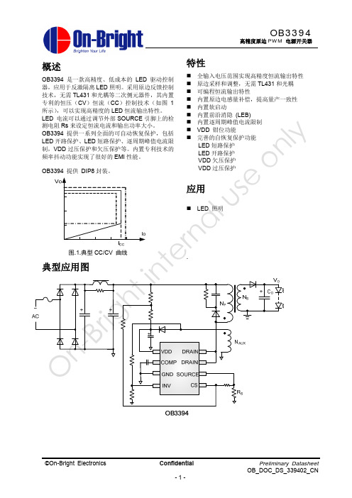
OB3394 Datasheet_CN_sz_110915
5
20 uA
I DD op
工作电流
ly UVLO(ON) n UVLO(OFF)
VDD_clamp
VDD 欠压保护(ON)阈值 VDD 欠压保护(OFF)阈值 VDD 钳位电压
o OVP
VDD 过压保护阈值
se Current Sense Input Section
u TLEB
前沿消隐时间
l Vth_oc
Min
Max
3.710
5.334
0.381
2.921
4.953
0.350
0.650
1.524 (BSC)
0.200
0.360
9.000
10.160
6.096
7.112
Dimensions In Inches
Min
Max
0.146
0.210
0.015
0.115
0.195
0.014
0.026
0.06 (BSC)
©On-Bright Electronics
Confidential -2-
Preliminary Datasheet OB_DOC_DS_339402_CN
标识信息
OB3394
高精度原边 PWM 电源开关器
al use only 引脚说明
rn Pin Num Pin Name I/O Description
6
SOURCE
5
CS
l use 定购信息 型号 On-Bright interna OB3394AP
描述 DIP8, Pb-free, Tube
VDD 电压 VDD 稳压管钳位电流 COMP 电压 CS 输入电压 INV 输入电压 最小/最大工作结温 TJ 最小/最大储藏温度 Tstg 管脚焊接温度(10secs)
Freescale 34933 双极桥驱动器说明说明书
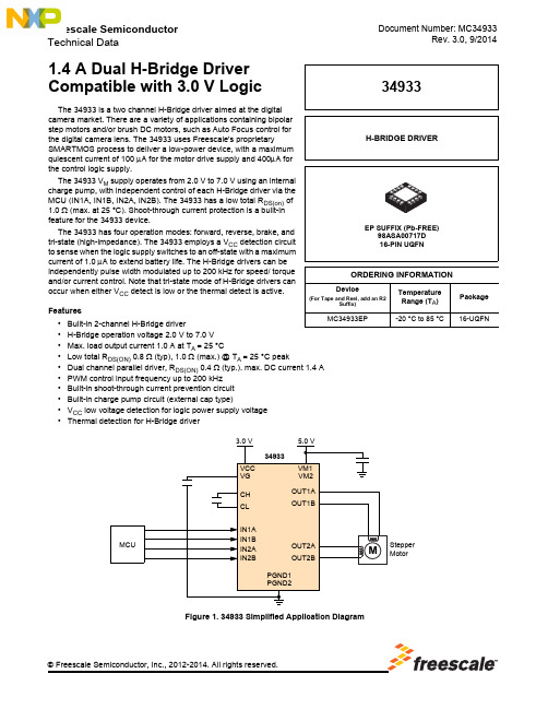
Document Number: MC34933Rev. 3.0, 9/2014Freescale Semiconductor Technical Data© Freescale Semiconductor, Inc., 2012-2014. All rights reserved.1.4 A Dual H-Bridge Driver Compatible with 3.0 V LogicThe 34933 is a two channel H-Bridge driver aimed at the digital camera market. There are a variety of applications containing bipolar step motors and/or brush DC motors, such as Auto Focus control for the digital camera lens. The 34933 uses Freescale's proprietarySMARTMOS process to deliver a low-power device, with a maximum quiescent current of 100 μA for the motor drive supply and 400μA for the control logic supply.The 34933 V M supply operates from 2.0 V to 7.0 V using an internal charge pump, with independent control of each H-Bridge driver via the MCU (IN1A, IN1B, IN2A, IN2B). The 34933 has a low total R DS(on) of 1.0 Ω (max. at 25 °C). Shoot-through current protection is a built-in feature for the 34933 device.The 34933 has four operation modes: forward, reverse, brake, and tri-state (high-impedance). The 34933 employs a V CC detection circuit to sense when the logic supply switches to an off-state with a maximum current of 1.0 μA to extend battery life. The H-Bridge drivers can be independently pulse width modulated up to 200 kHz for speed/ torque and/or current control. Note that tri-state mode of H-Bridge drivers can occur when either V CC detect is low or the thermal detect is active.Features •Built-in 2-channel H-Bridge driver•H-Bridge operation voltage 2.0 V to 7.0 V •Max. load output current 1.0 A at T A = 25 °C•Low total R DS(ON) 0.8 Ω (typ), 1.0 Ω (max.) @ T A = 25 °C peak•Dual channel parallel driver, R DS(ON) 0.4 Ω (typ.). max. DC current 1.4 A •PWM control input frequency up to 200 kHz •Built-in shoot-through current prevention circuit •Built-in charge pump circuit (external cap type)•V CC low voltage detection for logic power supply voltage •Thermal detection for H-Bridge driverFigure 1. 34933 Simplified Application Diagram34933ORDERING INFORMATIONDevice(For Tape and Reel, add an R2Suffix)Temperature Range (T A )Package MC34933EP-20 °C to 85 °C16-UQFNH-BRIDGE DRIVERAnalog Integrated Circuit Device Data34933INTERNAL BLOCK DIAGRAMINTERNAL BLOCK DIAGRAMFigure 2. 34933 Simplified Internal Block DiagramVCC DETECTIONTHERMAL DETECTIONCONTROL LOGICVGCH CLVCCIN1AIN1BIN2AIN2B* VM1 and VM2 are connected internally. Both VM1 and VM2 must be tied together on the PCB.PGND1 and PGND2 are connected internally. Both PGND1 and PGND2 must be tied together on the PCB.CHARGE PUMPVCCVM VG =VM+VCCVCCdetVCCtdetVCCVCCVCCdet tdetLEVEL SHIFTER PRE-DRIVERVCC VGVM1OUT1A OUT1BPGND1VM2OUT2A OUT2BPGND2Low-side DriverHigh-side DriverLow-side DriverHigh-side DriverAnalog Integrated Circuit Device Data 34933PIN CONNECTIONSPIN CONNECTIONSFigure 3. 34933 Pin ConnectionsTable 1. 34933 Pin DefinitionsPin NumberPin Name Pin FunctionFormal Name Definition1OUT1A Output H-Bridge Output 1A Output A of H-Bridge channel 1.2PGND1Power supply Power Ground 1Power supply grounds for the 34933 device. Refer to the application diagram for recommended layout.3PGND2Power supplyPower Ground 2Power supply grounds for the 34933 device. Refer to the application diagram for recommended layout.4OUT2A Output H-Bridge Output 2A Output A of H-Bridge channel 25OUT2B OutputH-Bridge Output 2BOutput B of H-Bridge channel 26VM2Power supply Motor Drive Power Supply 2Power supply pins for the 34933 motor drive circuitry. Refer to the application diagram for recommended layout.7IN2A Input Logic Input Control 2ALogic input control of OUT2A 8IN2B Input Logic Input Control 2B Logic input control of OUT2B 9IN1B Input Logic Input Control 1B Logic input control of OUT1B 10IN1A InputLogic Input Control 1ALogic input control of OUT1A11VCC Power supply Control Logic Power SupplyPower supply for the control logic circuitry.12VG Output Charge Pump OutputCapacitor Charge pump output pin connected to an external capacitor. The V G voltage is the sum of the V CC and V M power supplies.13CL Input/Output Charge Pump Capacitor 1Low-side charge pump capacitor connection 14CH Input/OutputCharge Pump Capacitor 2High-side charge pump capacitor connection15VM1Power supply Motor Drive Power Supply 1Power Supply pins for the 34933 motor drive circuitry. Refer to the application diagram for recommended layout.16OUT1BOutputH-Bridge Output 1BOutput B of H-Bridge channel 117(1)Exposed Pad Power supply EPThe exposed pad is connected to ground plane via the exposed pad solder pad. Note the primary purpose of the exposed pad for 34933 is thermal heat dissipation. Therefore, adequate thermal vias should be included in the PCB design.Notes1.Exposed pad is used as a heat sink. Connect it to the power ground through four thermal vias where the area is wide.U T 1BM 1HLI N 2I N 2V M O U T 2OUT2A PGND2PGND1OUT1AAnalog Integrated Circuit Device Data34933ELECTRICAL CHARACTERISTICS MAXIMUM RATINGSELECTRICAL CHARACTERISTICSMAXIMUM RATINGSTable 2. Maximum RatingsAll voltages are with respect to ground unless otherwise noted. Exceeding these ratings may cause a malfunction or permanent damage to the device.RatingsSymbolValueUnitELECTRICAL RATINGSControl Logic Power Supply Voltage VCC -0.5 to +6.0V Motor Drive Power SupplyVM -0.5 to +7.5V VCC Level Pin Voltage - IN1A, IN1B, IN2A, IN2BVpin1 -0.5 to +5.5V VM Level Pin Voltage - OUT1A, OUT1B, OUT2A, OUT2B, CL Vpin2 -0.5 to +7.5V VM+VCC Level Pin Voltage - CH, VGVpin3 -0.5 to +13.5V Motor Drive Maximum Load Current, T A = 85 °C I LOAD_DC_MD 0.7 A Motor Drive Maximum Load Current, T A = 25 °C I LOAD_DC_MD 1.0 A Motor Drive Maximum Peak Load Current (3)I LOAD_PEAK_MD1.4A Power Dissipation (4)P D 1.0W ESD Voltage (2)Human Body Model (HBM)Machine Model (MM)Charge Device Model (CDM)V ESD±4000±350±1000VTHERMAL RATINGSOperating Temperature Range T A -20 to +85 °C Operating Junction Temperature T J 150 °C Storage Temperature Range T STG-65 to +150°CTHERMAL RESISTANCEThermal Resistance, Junction to Case (5)R θJC 23︒C/W Peak Package Reflow Temperature During Reflow (6), (7)T PPRTNote 7°CNotes 2.ESD testing is performed in accordance with the Human Body Model (HBM) (C ZAP = 100 pF, R ZAP = 1500 Ω), the Machine Model (MM) (C ZAP = 200 pF, R ZAP = 0 Ω), and the Charge Device Model (CDM), Robotic (C ZAP = 4.0 pF).3.Peak time is for 10 ms pulse width at 200 ms intervals. T A = 25°C.4.R θJA = 50 °C/W, in case of 2s2p printed circuit board that defined on SEMI JEDEC JESD51- 3 and JESD51-6.5.Thermal resistance between the die and the case top surface as measured by the cold plate method (MIL SPEC-883 Method 1012.1).6.Pin soldering temperature limit is for 10 seconds maximum duration. Not designed for immersion soldering. Exceeding these limits may cause malfunction or permanent damage to the device.7.Freescale’s Package Reflow capability meets Pb-free requirements for JEDEC standard J-STD-020C. For Peak Package ReflowTemperature and Moisture Sensitivity Levels (MSL), go to , search by part number [e.g. remove prefixes/suffixes and enter the core ID to view all orderable parts. (i.e. MC33xxxD enter 33xxx), and review parametrics.Analog Integrated Circuit Device Data 34933ELECTRICAL CHARACTERISTICSSTATIC AND DYNAMIC ELECTRICAL CHARACTERISTICSSTATIC AND DYNAMIC ELECTRICAL CHARACTERISTICSTable 3. Static and Dynamic Electrical CharacteristicsCharacteristics noted under conditions, VM = 5.0 V, VCC = 3.0 V, unless otherwise noted. Typical values noted reflect the approximate parameter means at T A = 25 °C under nominal conditions, unless otherwise noted.CharacteristicSymbolMinTypMaxUnitPOWER SUPPLYMotor Drive Power Supply Voltage V M 2.0 5.0 7.0V Control Logic Power Supply VoltageV CC 2.73.05.5V Driver Quiescent Supply Current (IN1A, IN1B,IN2A, IN2B = L)No Signal InputI QM-72100uALogic Quiescent Supply Current (IN1A, IN1B, IN2A, IN2B = L)No Signal InputI QVCC-114400uAControl Logic Power Supply Operating Current (IN1A, IN2A = L, IN1B, IN2B = 200kHz)I VCC -350800uA Charge Pump Target VoltageVM = 2.0 V, VCC = 2.7 V, I LOAD = 0A VM = 5.0 V, VCC = 3.0 V, I LOAD = 0A VM = 7.0 V, VCC = 5.5 V, I LOAD = 0A V G4.27.612.04.457.812.34.78.012.5VCharge Pump Wake-up TimeCharge pump is enabled in V CC > V CCDET T VGON-130400usDriver Quiescent Supply Current at VCCDET = L V M = 5.0 V, V CC = 0 VI QM_VCD = L-- 1.0uACharge Pump Switching Frequency F QP -150-kHzH-BRIDGE DRIVERH-Bridge Driver High/Low-side Driver On-Resistance 1V CC = 2.7 V, I SINK = 100 mA, T A = 25 °CR ON1-0.40.45ΩH-Bridge Driver High/Low-side Driver On-Resistance 2 (8)V CC = 2.7 V, I SINK = 700 mA, T A = 25 °CR ON2-0.430.51ΩH-Bridge Driver High/Low-side Driver On-Resistance 3 (8)V CC = 2.7 V, I SINK = 700 mA, T A = 85 °CR ON3-0.510.62ΩH-Bridge Driver High/Low-side Driver On-Resistance 4V CC = 3.0 V, I SINK = 100 mA, T A = 25 °CR ON4-0.390.43ΩH-Bridge Driver High/Low-side Driver On-Resistance 5 (8)V CC = 3.0 V, I SINK = 700 mA, T A = 25 °CR ON5-0.410.48ΩH-Bridge Driver High/Low-side Driver On-Resistance 6 (8)V CC = 3.0 V, I SINK = 700 mA, T A = 85 °CR ON6-0.490.58ΩH-Bridge Driver Output Body Diode Forward Voltage I f = 100 mAV F-0.81.2VInput Pulse Frequency (INA/B)Duty of input signal = 50 %F IN--200kHzNotes8.Guaranteed by designAnalog Integrated Circuit Device Data34933ELECTRICAL CHARACTERISTICSSTATIC AND DYNAMIC ELECTRICAL CHARACTERISTICSH-BRIDGE DRIVER (CONTINUED)H-Bridge Output Propagation Delay Time for OUTA/B (H to L)R LOAD = (1.0 k Ω) between OUTA and OUTB (refer to Figure 4) (IN1A, IN2A = L, IN1B, IN2B = 200 kHz)t PDHL-0.10.5usH-Bridge Output Propagation Delay Time for OUTA/B (L to H)Rload = (1.0 k Ω) between OUTA and OUTB (refer to Figure 4) (IN1A, IN2A = L, IN1B, IN2B = 200 kHz)t PDLH-0.10.5us H-Bridge Output Pulse WidthR LOAD = 20 Ω between OUTA and OUTB, Input Pulse Width = 1.0 μs, 50% to 50%, t PW : 50% to 50% (refer to Figure 5)t PW0.7--usH-Bridge Output Propagation Delay Time (Hi-Z to H) (8)R LOAD = 100 k Ω to 1/2*VM, C LOAD = 0 pF, t PDZH 50% to 75%t PDZH--0.5usH-Bridge Output Propagation Delay- Time (H to Hi-Z) (8)R LOAD = 100 k Ω to 1/2*VM, C LOAD = 0 pF, t PDHZ 75% to 50%t PDHZ-- 2.0usCONTROL LOGICHigh Level Input Voltage (IN1A, IN1B, IN2A, IN2B)V CC = 2.7 V ~ 5.5 VV IHV CC x0.7--VLow Level Input Voltage (IN1A, IN1B, IN2A, IN2B)V CC = 2.7 V ~ 5.5 VV IL--V CC x0.3V High Level Input Current (IN1A, IN1B, IN2A, IN2B)V TERMAINAL1 = 3.0 VI IH9-20uALow Level Input Current (IN1A, IN1B, IN2A, IN2B)V CC = 2.7 V to 5.5 VI IL-1.0--uAInput Pulse Rise Time (IN1A, IN1B, IN2A, IN2B)V CC = 2.7 V to 5.5 Vt R-- 1.0usInput Pulse Fall Time (IN1A, IN1B, IN2A, IN2B)V CC = 2.7 V to 5.5 V t F-- 1.0usDETECTORVCC Detection Voltage (refer to Figure 6)V CCDET 2.0 2.2 2.4V VCC Detection hysteresis Voltage (refer to Figure 6)V CCDETHYS0.050.10.3V Thermal Detection Temperature (9)T DET 150170190°C Thermal Detection Hysteresis Temperature (9)T DETHYS102030°CNotes9.Guaranteed by designTable 3. Static and Dynamic Electrical CharacteristicsCharacteristics noted under conditions, VM = 5.0 V, VCC = 3.0 V, unless otherwise noted. Typical values noted reflect the approximate parameter means at T A = 25 °C under nominal conditions, unless otherwise noted.CharacteristicSymbolMinTypMaxUnitAnalog Integrated Circuit Device Data 34933ELECTRICAL CHARACTERISTICSTIMING DIAGRAMSTIMING DIAGRAMSFigure 4. t PDLH and t PDHL TimingFigure 5. t PW TimingFigure 6 and Figure 7 show the timing charts of input and output signalsTable 4. Truth TableINPUTOUTPUTVccdetTdetIN1A IN2AIN1B IN2B OUT1A OUT2A OUT1B OUT2B L X X X Z Z H L L L L L H L H L H L H L L H L H H L HH Z Z HHXXZZH - High L - LowZ - High-impedanceX - Don’t CareAnalog Integrated Circuit Device Data34933ELECTRICAL CHARACTERISTICS TIMING DIAGRAMSFigure 6. Timing Chart of Input and Output Signal (V CCDET case)Figure 7. Timing Chart of Input and Output Signal (t DET case)Analog Integrated Circuit Device Data 34933FUNCTIONAL DESCRIPTION FUNCTIONAL PIN DESCRIPTIONFUNCTIONAL DESCRIPTIONFUNCTIONAL PIN DESCRIPTIONLOGIC SUPPLY (VCC)The VCC pin carries the logic supply voltage and current into the logic sections of the IC. VCC has an under-voltage threshold. If the supply voltage drops below the under-voltage threshold, the output power stage switches to a tri-state condition. When the supply voltage returns to a level that is above the threshold, the power stage automatically resumes normal operation according to the established condition of the input pins.LOGIC INPUT CONTROL (IN1A, IN1B, IN2A, AND IN2B)These logic input pins control each H-Bridge output. IN1A logic HIGH = OUT1A HIGH. However, if all inputs are HIGH, the output bridges are both tri-stated (refer to Table 4, Truth Table).H-BRIDGE OUTPUT (OUT1A, OUT1B, OUT2A, AND OUT2B)These pins provide connection to the outputs of each of the internal H-Bridges (See Figure 2, 34933 Simplified Internal Block Diagram).MOTOR DRIVE POWER SUPPLY (VM1 AND VM2)The VM pins carry the main supply voltage and current into the power sections of the IC. This supply then becomes controlled and/or modulated by the IC as it delivers the power to the loads attached between the output pins. All VM pins must be connected together on the Printed Circuit Board (PCB).CHARGE PUMP (CL AND CH)These two pins, the CL and CH, connect to the external bucket capacitors required by the internal charge pump. The typical value for the bucket capacitors is 0.1 μF.POWER GROUND (PGND)Power ground pins must be tied together on the PCB and connected to the common ground plane.LOGIC GROUND (EXPOSED PAD)The Exposed Pad is connected to the PCB Ground plane through vias by soldering. Note the primary purpose of the Exposed pad for 34933 is thermal heat dissipation.Therefore, adequate thermal vias should be included in the PCB design. The exposed pad should be connected to the common ground plane.VOLTAGE DETECTION AND THERMAL LIMIT DETECTIONThe 34933 has the VCC Low Voltage Detection (Vccdet) and the Thermal Detection (T DET ). VCC Low Voltage Detec-tion is designed to shutdown of IC functions when VCC becomes lower than specified voltage. Thermal Detection operates when the IC temperature exceeds specified valueand stop H-Bridge operation. Table 5 shows block status of 34933 by each condition. VCC is the control logic power supply for 34933. The system begins to operate when V CC > V CCDET (Typ. 2.2 V).Table 5. Block StatusOperation modeVccdet Tdet Charge PumpH-Bridge Driver1L X Disable Disable 2H L Enable Enable 3HHEnableDisableH - High L - LowX - Don’t CareTYPICAL APPLICATIONTYPICAL APPLICATIONFigure 8 shows a typical application using the 34933. The internal charge pump of this device is powered from the V CC supply. Therefore, care must be taken to ensure V CC is a high enough value to provide sufficient gate-source voltage for the high-side MOSFETs when V M > V CC (e.g., V M = 5.0 V, V CC = 3.0 V), in order to ensure full enhancement of the high-side MOSFET channels.The 34933 can be configured in several applications. The figure below shows the 34933 in a typical Slave Node Application.*1 - It is recommend to use low resistance copper PCB traces betweenVM & VCC ground and the PGND1/PGND2 pins.Figure 8. Typical Application34933Analog Integrated Circuit Device DataAnalog Integrated Circuit Device Data 34933PCB LAYOUTPCB LAYOUTWhen designing a printed circuit board (PCB), connect sufficient capacitance between power supplies (VM & VCC) and ground pins to ensure proper filtering from transients. For all high-current paths, use wide copper traces and theshortest possible distances. Note that capacitors should be placed as close to the 34933 as possible to maximize the filtering capability of each capacitor.Additionally, care must be taken to avoid CEMF spikes induced when inductive currents accumulate at the VM supply. The typical method of snubbing inductive spikes includes connecting a Zener diode or capacitor at the supplypin (VM).Analog Integrated Circuit Device Data34933PACKAGINGPACKAGE DIMENSIONSPACKAGINGPACKAGE DIMENSIONSPackage dimensions are provided in package drawings. To find the most current package outline drawing, go to and perform a keyword search for the drawing’s document number.Table 6.PackageSuffix Package Outline Drawing Number16-PIN UQFNEP98ASA00717DAnalog Integrated Circuit Device Data 34933PACKAGINGPACKAGE DIMENSIONS.Analog Integrated Circuit Device Data34933PACKAGINGPACKAGE DIMENSIONSAnalog Integrated Circuit Device Data 34933PACKAGINGPACKAGE DIMENSIONSAnalog Integrated Circuit Device Data34933REVISION HISTORYREVISION HISTORYREVISIONDATE DESCRIPTION OF CHANGES 2.07/2010•Initial Release.12/2013•No technical changes •Revised back page•Updated document properties 3.09/2014•Changed 98A to 98ASA00717D •Update formatDocument Number: MC34933Rev. 3.09/2014Information in this document is provided solely to enable system and software implementers to use Freescale products. There are no express or implied copyright licenses granted hereunder to design or fabricate any integrated circuits based on the information in this document.Freescale reserves the right to make changes without further notice to any products herein. Freescale makes no warranty, representation, or guarantee regarding the suitability of its products for any particular purpose, nor does Freescale assume any liability arising out of the application or use of any product or circuit, and specifically disclaims any and all liability, including without limitation consequential or incidental damages. “Typical” parameters that may be provided in Freescale data sheets and/or specifications can and do vary in different applications, and actual performance may vary over time. All operating parameters, including “typicals,” must be validated for each customer application by customer’s technical experts. Freescale does not convey any license under its patent rights nor the rights of others. Freescale sells products pursuant to standard terms and conditions of sale, which can be found at the following address: /SalesTermsandConditions .Freescale and the Freescale logo are trademarks of Freescale Semiconductor, Inc., Reg. U.S. Pat. & Tm. Off. SMARTMOS is a trademark of Freescale Semiconductor, Inc. All other product or service names are the property of their respective owners.© 2014 Freescale Semiconductor, Inc.How to Reach Us:Home Page: Web Support:/support。
C339C_datasheet
TYP. ±2 ±5 25 200 0.8
0.2 16 0.1 1.3
MAX. ±5 ±50 250
2 V+–1.5
0.4
Unit mV nA nA V/mV mA V V mA nA µs
3
APPLICATION CIRCUIT EXAMPLE V+
4, 6, 8, 10
VIN
–
3
5, 7, 9, 11 +
Date Published February 1997 N Printed in Japan
©
1997
µPC339
ABSOLUTE MAXIMUM RATINGS (TA = 25 °C)
Parameter
Voltage between V+ and V–
Note 1
Differential Input Voltage
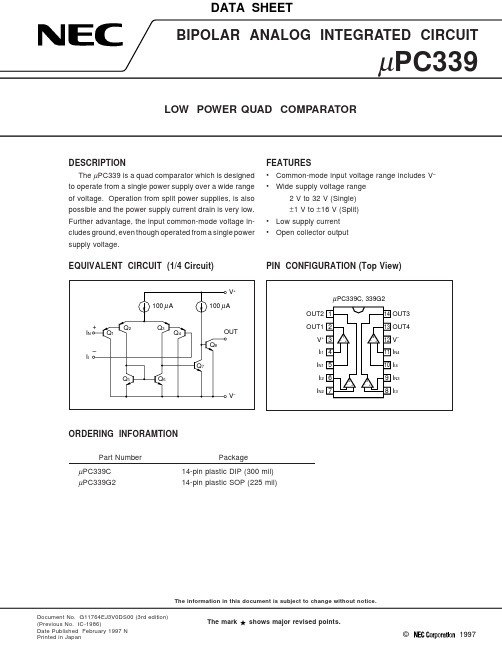
FEATURES • Common-mode input voltage range includes V– • Wide supply voltage range
2 V to 32 V (Single) ±1 V to ±16 V (Split) • Low supply current • Open collector output
0.1
1
10
100
பைடு நூலகம்
IO SINK - Output Sink Current - mA
5
VIN - Input Voltage - mV VO - Output Voltage - V VIN - Input Voltage - mV VO - Output Voltage - V
- 1、下载文档前请自行甄别文档内容的完整性,平台不提供额外的编辑、内容补充、找答案等附加服务。
- 2、"仅部分预览"的文档,不可在线预览部分如存在完整性等问题,可反馈申请退款(可完整预览的文档不适用该条件!)。
- 3、如文档侵犯您的权益,请联系客服反馈,我们会尽快为您处理(人工客服工作时间:9:00-18:30)。
保证声明 昂宝电子有限公司依从其标准保单书承诺,出售时所有硬件产品性能参数均符合产品的相应使用规格书。产
恒
OB3393S 提供一系列全面的可自动恢复保护,包 括 LED 开路保护、LED 短路保护、逐周期峰值电流
深 限制,VDD 过压保护、欠压保护和锁存的过温保护
等。
to OB3393S 提供 SOP-8 封装。
内置前沿消隐 (LEB) 完善的自恢复保护功能
LED 短路保护 LED 开路保护 VDD 欠压保护
8-Pin Plastic SOP
OB3393S
高精度原边反馈 LED 控制器
恒
ht Confidential to 深 Symbol ig A
A1
r A2
b
Bc -D
E
nE1 e
OL
Dimensions In Millimeters
Min
Max
1.350
1.750
0.050
0.250
1.250
1.650
I/O 描述 I 电流采样端
无连接,必须悬空
P 电源供电端 I 内部高压功率管源极 I 内部高压功率管漏极 P 无连接,必须悬空并且不要放置焊盘 P地
©On-Bright Electronics
Confidential 3
Preliminary Datasheet OB_DOC_DS_3393S00_CN
启动电流 工作电流 VDD 欠压保护(OFF)阈值 VDD 欠压保护(ON)阈值 VDD 钳位阈值
前沿消隐时间 恒流 OCP 阈值
Td_oc
芯片传输延迟
n Toff_max
最大 OFF 时间
e Toff_min
最小 OFF 时间
fid Ton_max
最大 ON 时间
源极驱动
n Rdson_l
源极驱动开关管导通阻抗
制技术,无需 TL431 和光耦等二次侧元器件;极低 高效率、低系统成本
的工作电流,无需辅助绕组供电和检测,芯片采用 可调节设定恒流输出特性
专利的恒流控制方式,实现高精度的 LED 恒流输出 特性。LED 电流可以通过调节外部 CS 引脚上的检 测电阻 Rs 来设定。
内置原边电感量补偿 内置线电压补偿 CC 内置逐周期峰值电流限制
0.310
0.510
0.100
0.250
4.700
5.150
3.800
4.000
5.800
6.200
1.270 (BSC)
0.400
1.270
Dimensions In Inches
Min
Max
0.053
0.069
0.002
0.010
0.049
0.065
0.012
0.020
0.004
0.010
0.185
OB3393S
高精度原边反馈 LED 控制器
概述
特性
OB3393S 是一款高精度、低成本的 LED 驱动控制 输入电压全范围实现高精度恒流输出特性
器,应用于反激隔离 LED 照明。
原边采样和调整,无需 TL431 和光耦
OB3393S 内部集成 650V 功率管,采用原边反馈控 极低的工作电流,无需辅助绕组供电和检测
Preliminary Datasheet OB_DOC_DS_3393S00_CN
OB3393S
高精度原边反馈 LED 控制器
基本信息
引脚排布 SOP-8 引脚图如下.
额定封装散热 封装 SOP-8
RθJA (℃/W) 150
.
CS
1
8 GND
应用极限参数 参数
规格
NC
2
7 GND
VDD 电压 DRAIN 电压
过温保护
l APPLICATIONS tia LED 照明
en 典型应用图
nfid ~
+
On-Bright Co AC
+
CS GND NC GND VDD Drain SW Drain
OB3393S
VLED
+ CO
NP
NS
©On-Bright Electronics
Confidential -1-
ZZZ:Lot Code
l C: SOP8 tia P:Pb-free Package
S:Character Code
n s: Internal Code(Optional)
fide 引脚说明
引脚号 1
n 2 o 3
4
C 5,6 t 7 On-Brigh 8
引脚说明 CS
NC
VDD SW DRAIN NC GND
Packing
Blank:Tube A: Tape/Reel
©On-Bright Electronics
Confidential -2-
Preliminary Datasheet OB_DOC_DS_3393S00_CN
标识信息
OB3393S
高精度原边反馈 LED 控制器
恒
深 Y: Year Code to WW: Week Code (01-52)
以确保客户产品及应用的风险降到最低。
to 医疗领域 l 昂宝电子有限公司的产品不可用于维持、延续人类生命等医疗设备,并对其产品被用于医疗领域所造成的任
何损害或索赔不承担任何法律责任。
tia 军用领域
昂宝电子有限公司的产品不可用于军用领域,并对其产品被用于军用领域所造成的任何损害或索赔不承担任
On-Bright Confiden 何法律责任。
CS 输入电压
-0.3 to 7V
SW 输入电压
-0.3 to 9V
最小/最大工作结温 TJ 最小/最大储藏温度 Tstg 管脚焊接温度(10secs)
-40 to 150 ℃ -55 to 150 ℃ 260 ℃
备注: 芯片的实际应用条件超出规定的“应用极限值”将会
对芯片造成永久性损伤。以上应用极限值标志了芯片可承
受应力等级,但并不建议芯片在此极限条件或超出“推荐工
作条件”下工作。芯片长时间处于最大额定工作条件,会影
响芯片的可靠性。
n OB3393S
X
X
X
On-Bright Confide High Precision Offline LED Power Switch
Package C:SOP8
Package Pb free P:Pb-free
恒 品的测试和其它质量管理技术可对此担保。除了某些政府要求的项目,没有必要对每个产品的所有参数进行
测试。 昂宝电子有限公司对产品应用方面的设计协助或客户产品的设计不具任何义务。客户产品中使用昂宝电子的
深 产品、性能规格书和使用说明书,客户应对自己的产品及应用负责。客户应提供适当的设计和操作保护措施,
o OTP Section
C OTP
过温保护温度
t Power MOSFET Section
BVdss
功率管漏极-源极击穿电压
On-Brigh Rds,on
功率管导通阻抗
VDD=UVLO(OFF)-1 VDD=7.5V
1mA
120 150 uA
160 320 uA
7
V
6
V
8
V
0.3
485 500
From OCP comparator to base drive
©On-Bright Electronics
Confidential -6-
Preliminary Datasheet OB_DOC_DS_3393S00_CN
恒 -0.3 to 18V
-0.3 to 650V
VDD 3
6 Drain
深 SW
4
5 Drain
to 定购信息
l 型号
描述
tia OB3393SCP
OB3393SCPA
8 Pin SOP, Pb free in Tube 8 Pin SOP, Pb free in T&R
备注: 如无特殊说明,器件提供的是无铅封装。
0.203
0.150
0.157
0.228
0.244
0.050 (BSC)
0.016
0.050
θ
0º
8º
0º
8º
©On-Bright Electronics
Confidential -5-
Preliminary Datasheet OB_DOC_DS_3393S00_CN
OB3393S
高精度原边反馈 LED 控制器
100
600
4.5 5
50
us 515 mV
ns
us 5.5 us
us
Static, Id=1A
1.3
ohm
150
℃
650
V
18
ohm
©On-Bright Electronics
Confidential -4-
Preliminary Datasheet OB_DOC_DS_3393S00_CN
封装结构信息
OB3393S
高精度原边反馈 LED 控制器
电气参数
(如无特殊说明,环境温度 TA = 25℃, VDD=7.5V)
符号
描述
测试条件
最 小 值
典 值