LinearLTC压电能量收集电源方案
linearltc压电能量收集电源方案
Lin earLTC3588-1 压电能量收集电源方案关键字:电源管理,能量收集器,DC/DC转换器Lin ear公司的LTC3588-1是压电能量收集电源,集成了低噪音全波整流和高效降压转换器,组成完整的能量收集解决方案,最适合高输出阻抗的能量源如压电传感器•输入电压2.7V-20V,输出电流高达100mA可选输出电压1.8V,2.5V,3.3V 和 3.6V,可用于压电能量收集,电-机械能量收集,无线HVAC专感器,轮胎压里传感器遥控光幵关,毫微瓦降压稳压器.本文介绍LTC3588-1主要特性,方框图以及多种应用电路图,包括100mA压电能量收集电源电路图,最小尺寸的1.8V低压输入压电能量收集电源电路图,电场能量和热电能量收集器电路图等•LTC3588-1:PiezoelectricE nergyHarvesti ngPowerSupplyTheLTC.3588-1i ntegratesalow-lossfull- wavebridgerectifierwithahighefficie ncybuckc on vertertoformacompletee nergy harvesti ngsoluti ono ptimizedforhighoutputimpeda ncee nergysourcessuchaspiez oelectrictra nsducers.A nultralowquiesce ntcurre ntun dervoltagelockout(UVLO) modewithawidehysteresiswi ndowallowschargetoaccumulate onanin putcapacitoru n tilthebuckc on verterca nefficie ntlytra nsferaportio no fthestoredchargetothe output.I nregulatio n,theLTC3588-1en tersasleepstate in whichboth in puta ndoutputquiesce ntcurre ntsare mini mal.T hebuckc on vertertur nsonan doffas neededtoma intain regulati on.Fouroutputvoltages,1.8V,2.5V,3.3Va nd3.6V,arepi nselectablewithupto100m Aofcontinu ousoutputcurre nt;however,theoutputcapacitormaybesizedtoservice ahigheroutputcurre ntburst.A nin putprotectivesh un tsetat20Ve nablesgreatere n ergystorageforagive namoun tofi nputcapacita nee.LTC3588-1主要特性:—NoLoad) 950nAln putQuiesce ntCurre nt(Outputi nRegulatio n450nAI nputQuiesce ntCurre nti nUVLO2.7Vto20VI nputOperati ngRa ngeIn tegratedLow-LossFull-WaveBridgeRectifierUptolOOmAofOutputCurre nt SelectableOutputVoltagesof1.8V,2.5V,3.3V,3.6VHighEfficie ncyl ntegratedHystereticBuckDC/DCIn putProtectiveShu nt —Upto25mAPull-Do wn atVIN> 20V WideI nputU ndervoltageLockout(UVLO)Ra ngeAvailablei n10-LeadMSEa nd3mmx3mmDFNPackagesLTC3588-1 应用:PiezoelectricE nergyHarvesti ngElectro-Mecha nicalE nergyHarvesti ngWirelessHVACSe nsors MobileAssetTracki ngTirePressureSe nsors BatteryReplaceme ntforl ndustrialSe nsors RemoteLightSwitchesStan dal on eNa nopowerBuckRegulator著一m函1.LTC3588匕8斎函」sm ApieicE一鱼S-rrl n E a yHaw邕?壬『OCT函 2.L T C3588—l 00m A te [>^K *t >[>M函i图3.LTC3588-13.3V 压电能量收集电源电路图:给带无线发送器的微处理器和 50mA 瞬态负载供电.P 旧电 SYSTEMS T220-.M*^3X_IDI —图4.最小尺寸的1.8V 低压输入压电能量收集电源电路图'h {OPTIONAL}VlH PGCXJDV||Q LTCK3B-1CAPsw D3 VoufDO1O|1FprePGOOOLTC3588-1$w^bur、蟻bl 1帕&0PIEZO STS T230-A4-M3XTtzu=1=T1-q —刖M|lF &vPflPZ? KWCW*|hUC358B-1.B . ¥IIE ■aiiiDI&3GND—■ JU -10UHI J-111FT2Li 卯—r- ?5V I -------1±图5.采用单个压电晶体和自动加电次序的双电源电路图iMU 比4优罚TWIflUHVOUTipF 6V—r^Ev1O0^亠*髦"F "T BYr1OyF25V I ----------------47|f图6.带备份电池的压电能量收集器电路图图7.AC 火线供电的3.6V 降压稳压器,大输出电容支持重负载PANELS ARE PLACED G bFROM T x4' FLUQRfSCFFJT LiflHT FIXTURESGOPPtR 用MEL(情綁刊IDANGER! HIGH VOLTAGE'COPPER PA 忡EL(12* x 24f \—F*GOODPGOQD9V ' BAntHVP1E2O SVSTEMS T2SOW-503XP21p 竝VlHPGOODITG33A8-1CAP SWV|W2Van00P22GHDPGOODPZ2PGOODlTCJ5B8-tswV,-,-vgyr□ lDO RND5p7?v-iPGOODLTO5^0-1GAP5W%V QUTBlI (X JHJ —*1O^F "T" SV图8.电场能量收集器电路图St _L5VT0 f6V•…SOUR PANfL rao5M4X&FrrIPF■VvVT BATTERYII%PiJOODLTG3W1GAP SWy IV3V CVT0001GNDiPG3OD5* 2.7V 蚀FX5V NESS SUPER W^ACITOR_ £5HSR-ODa30O^M2fl7图9.5-16V太阳能供电的2.5V电源,其超大电容增加输出能量存储和备份电池IPG-1 THERMALI GEMERATORMi 61-1,0-127-1.27I (TELLUflEX)—5,4VH工工工[---------1P22%卩GOODUC3506-1CAP畑V OUTDO01GUO跡47pF2.5V图10.热电能量收集器电路图。
Linear LTC4000高压电池充电解决方案
Linear LTC4000高压电池充电解决方案Linear公司的LTC4000是高压高性能电池充电控制器,输入和输出电压宽达3V到60V,输入和充电电流精度在±1%,可编程浮电压精度±0.25%,可选择的定时器和终止充电电流,采用NTC热电阻的温度补偿充电,自动再充电,不良电池检测和用于深度放电电池的C/10涓流充电以及状态指示输出.主要用在大功率电池充电系统,高性能手持仪表,笔记本/亚笔记本电脑等.本文介绍了LTC4000主要特性,方框图, 用于三个LiFePO4电池的48-10.8V/10A降压充电器电路图以及用于单个和多个锂离子电池充电器电路图.The LTC®4000 is a high voltage, high performance controller that converts many externally compensated DC/DC power supplies into full-featured battery chargers. Features of the LTC4000’s battery charger include: accurate (±0.25%) programmable float voltage, selectable timer or current termination, temperature qualified charging using an NTC thermistor, automatic recharge, C/10 trickle charge for deeply discharged cells, bad battery detection and status indicator outputs. The battery charger also includes precision current sensing that allows lower sense voltages for high current applications.The LTC4000 supports intelligent PowerPath control. An external PFET provides low loss reverse current protection.Another external PFET provides low loss charging or discharging of the battery. This second PFET also facilitates an instant-on feature that provides immediate downstream system power even when connected to a heavily discharged or short faulted battery.The LTC4000 is available in a low profile 28-lead 4mmx5mm QFN and SSOP packages.LTC4000主要特性:Complete High Performance Battery Charger When Paired with a DC/DC ConverterWide Input and Output Voltage Range: 3V to 60VInput Ideal Diode for Low Loss Reverse Blocking and Load SharingOutput Ideal Diode for Low Loss PowerPath™ and Load Sharing with the BatteryInstant-On Operation with Heavily Discharged BatteryProgrammable Input and Charge Current:±1% Accuracy±0.25% Accurate Programmable Float VoltageProgrammable C/X or Timer Based Charge TerminationNTC Input for Temperature Qualified Charging28-Lead 4mm 5mm QFN or SSOP PackagesLTC4000应用:High Power Battery Charger SystemsHigh Performance Portable InstrumentsIndustrial Battery Equipped DevicesNotebook/Subnotebook Computers图1.LTC4000方框图图2.LTC4000用于三个LiFePO4电池的48-10.8V/10A降压充电器电路图(1)图3.用于LTC4000的Kelvin检测线的配置框图图 4.LTC4000用于三个LiFePO4电池的48-10.8V/10A降压充电器电路图(2)图5.LTC4000用于五个锂离子电池的6-12V/5A降压充电器电路图图6.LTC4000用于单个锂离子电池的18V-72VIN输入的4.2V/5A绝缘反激充电器电路图详情请见:/docs/Datasheet/4000p.pdf。
压电能量管理芯片的整流电路和欠压锁定电路
压电能量管理芯片的整流电路和欠压锁定电路引言:尽管能量管理的概念广为人知已有多年,但在某种实际环境中实现这样一个系统却十分麻烦、复杂和昂贵。
然而,采用了能量管理方法的市场实例包括交通运输基础设施、无线医疗设备、轮胎压力检测,而迄今为止最大的市场便是楼宇自动化。
就楼宇自动化而言,诸如占有传感器、温度自动调节器和光开关等系统能够免除通常所需的电源或控制线路,取而代之是一个机械或能量收集系统。
同样,运用能量管理技术的无线网络能够将建筑物内任何数目的传感器连接起来,以在无人值守情况下通过切断非紧要区域的供电来降低采暖、通风和空调以及照明成本。
此外,能量管理电子线路的成本常常低于电源线路的运行成本,因此,选用管理电能技术显然能够带来经济上的收益。
1.压电管理芯片的工作原理压电能量管理芯片,顾名思义,它负责管理能量。
主要功能:负责给手机各部分分配电压、做电平转换、AD/DA转换等。
下面我们主要以NOKIA 6120C为例子来看一下管理器的内部一种结构。
AVILMA和BETTY搭配结构用到的芯片:AVILMA_1.05C 这个芯片比较个性,网上根本找不到她的datasheet,应该是NOKIA向那个厂商定制的芯片。
但是它的个性之处不在于定制,而是功能。
她集成了两路音频功放(从图上可以看到,应该分别对应的手机听筒和外放),SIM卡的读取,电源按键的控制,MIC 的放大和数字采样,当然还有与主控CPU的通信功能很杂。
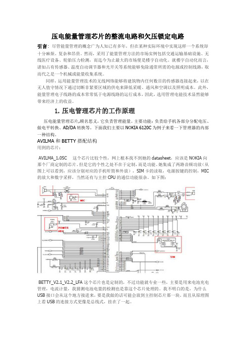
如下图:BETTY_V2.1_V2.2_LFA 这个芯片也是定制的,不过功能就专业一些,主要是用来电池充电管理,电流计量,我猜测电池电量的检测也是靠这个芯片处理的。
我不明白的是,为什么USB接口会从这个地方接进来,要是我做的话可能会放到主控制芯片那一块。
而且从原理图上看USB的连接方式更像是总线式,挂在了一起。
2.整流电路的原理和结构整流电路(rectifying circuit)把交流电能转换为直流电能的电路。
LinearLTC3588~1压电能量收集电源方案
Lin ear LTC3588-1压电能量收集电源方案关键字:电源管理,能量收集器,DC/DC转换器Linear公司的LTC3588-1是压电能量收集电源,集成了低噪音全波整流和高效降压转换器,组成完整的能量收集解决方案,最适合高输岀阻抗的能量源如压电传感器•输入电压2.7V-20V,输岀电流高达100mA,可选输出电压1.8V, 2.5V, 3.3V和3.6V,可用于压电能量收集,电-机械能量收集无线HVAC传感器,轮胎压里传感器,遥控光开关,毫微瓦降压稳压器.本文介绍LTC3588-1主要特性,方框图以及多种应用电路图,包括100mA压电能量收集电源电路图,最小尺寸的1.8V低压输入压电能量收集电源电路图,电场能量和热电能量收集器电路图等.LTC3588-1: Piezoelectric Energy Harvesting Power SupplyThe LTC.3588-1 integrates a low-loss full-wave bridge rectifier with a high efficiency buck converter to form a complete energy harvesting solution optimized for high output impedance energy sources such as piezoelectric transducers. An ultralow quiescent current undervoltage lockout (UVLO) mode with a wide hysteresis window allows charge to accumulate on an input capacitor until the buck converter can effi ciently transfer a portion of the stored charge to the output. In regulation, the LTC3588-1 enters a sleep state in which both input and output quiescent currents are minimal. The buck converter turns on and off as needed to maintain regulation.Four output voltages, 1.8V, 2.5V, 3.3V and 3.6V, are pin selectable with up to 100mA of continuous output current; however, the output capacitor may be sized to service a higher output current burst. An input protective shunt set at 20V enables greater energy storage for a given amount of input capacitance.LTC3588-1主要特性:950nA Input Quiescent Current (Output in Regulation - No Load)450nA Input Quiescent Current in UVLO2.7V to 20V Input Operating RangeIntegrated Low-Loss Full-Wave Bridge RectifierUp to 100mA of Output CurrentSelectable Output Voltages of 1.8V, 2.5V, 3.3V, 3.6VHigh Efficiency Integrated Hysteretic Buck DC/DCInput Protective Shunt - Up to 25mA Pull- Down at VIN > 20V Wide Input Undervoltage Lockout (UVLO) RangeAvailable in 10-Lead MSE and 3mm x3mm DFN Packages LTC3588-1 应用:Piezoelectric Energy HarvestingElectro-Mechanical Energy HarvestingWireless HVAC SensorsMobile Asset TrackingTire Pressure SensorsBattery Replacement for Industrial SensorsRemote Light SwitchesStandalone Nanopower Buck Regulator6恤10, 血IIHErUIAl FUILE 31 01 M)L} "T —6V图2.LTC3588-1 100mA 压电能量收集电源电路图图1.LTC3588-1方框图 100mA Piezoelectric Energy Harvesting Power Su 叩ly ACVAWCEO CERAMETPICS PFC-WU BUCK :CCNrROLCSIORAGE25Y rIQpH---- -------------------- 畑 TI 丄< 砒 _H 刖nMi■ ] OUTPUT - ~ VOLTAGESELECTPGOOi?PGOODGWFRFJGR0ALD&APREFERENCE PZ1 PZ2v,Nsw n«&se -i如CAPPGOOO VlPiz00. Q1GRID工图 3.LTC3588-1 3.3V 压电能量收集电源电路图:给带无线发送器的微处理器和50mA 瞬态负载供电.图5.采用单个压电晶体和自动加电次序的双电源电路图PZ1VinmPGOODCAPLTG35W-1 鬧畑hiv tMHU ID9GMDCO^EENhMICROPROCESSORL.・ OpF I --------------------- ' 丄斗卉4 uS图4.最小尺寸的1.8V 低压输入压电能量收集电源电路图眺JO £*STLUSPZ2PZI PGODDDO10pF25V pdOO 序一1—MF "Rev rLTCJsea-iCAP SW图8.电场能量收集器电路图图6•带备份电池的压电能量收集器电路图图7.AC 火线供电的3.6V 降压稳压器,大输出电容支持重负载円㈣:”DANGER HIGH VOLTAGE 1150k信 DkI------------- z\l20VAC创用 1 5Qk 15CH<-T-弭9VBAHEHVPILZO SVSTEMS T22O-W-5WXtR05H40C&?7^rtFPANELS ARE PLACED G bFROM ?' x4' FLUORfSCEM LIGHT FiZTUFtESCCPPfR PAF1ELCOPPER 朋毗LP22V|kjPGOODITC358 &>1CftpSW V|H2VtMJT口DOGHCIF'A QOCP71 P7? V.|PGOODLTC3&B0-13Wv12 VOUTtnGMDPGOOD±±GU二询s图10.热电能量收集器电路图图9.5-16V 太阳能供电的2.5V 电源,其超大电容增加输出能量存储和备份电池10012I Pfi-1 THERMAL |鉅碰RATOR fflie 1-1,0-127-157I llfLLJflEKi丁阳 •ipf ■仙mi -w>5V TO 16VSOLAR PAN5LSVRAnERY[R06H4X5FTRM : HE255 S' PER TAPACiTOR TAW :RF1-'00300-^237—^— i OpfPGO QDP12WinPG&ODLTC358 时CAPBVJ恤0001 GND—團 - |'"4.7|jF 工PZ1PZ2 wPG-OTDLTG35S8-1CAPSW 畑VOUT :DOD1GNDPGOOO。
基于压电能量收集技术的充电器设计
基于压电能量收集技术的充电器设计摘要:为了解决利用压电能量收集技术收集到电能的存储问题,提出了一种充电器的设计方案。
利用压电能量收集器和LTC3588—1电源管理芯片为核心的电压变换电路以及LTC4071充电控制芯片为核心的充电控制电路,将收集到的电能变换后存储到锂电池。
实验结果表明,设计的充电器能够输出4.1V的稳定直流电压来为锂电池充电,实现了将压电能收器收集的电能存储到锂电池,具有应用前景。
引言近年来,能量的收集日益引起人们的关注。
能量收集是近年来在能源危机中发展出来的一个新兴名词,和传统的发电机产生电能的方式不同,能量收集是希望将环境中所未能利用的能源将其转换成人们可以使用的电能然后存储,以达到能源回收再利用的目的。
由于压电材料具有响应速度快,成本低,结构简单等优点,基于压电材料的能量收集技术已经成为了一种很有发展前途的能量收集方式,压电材料通过压电效应可以将周围的振动能量转换成电能。
由于压电能量收集器产生的电能电压大、电流小、功率小,而且是交流电压。
因此不能直接供给电子器件使用,需要先将收集的电能进行变换,然后存储后才能向外供电。
鉴于压电能量收集的电能存储问题,本文提出了一种基于压电能量收集技术的充电器的设计方案。
利用压电能量收集器和LTC3588-1电源管理芯片为核心的电压变换电路以及LTC4071充电控制芯片为核心的充电控制电路,将收集到的能量存储到锂电池。
研究了压电能量收集器在谐振状态下,充电器给锂电池充电的时间以及验证充电器充电电路的可行性。
1 压电能量收集器结构及工作原理压电能量收集器利用压电效应,可以将机械振动能量转换为电能。
悬臂梁式能量收集器结构是最常见的振动能量收集器结构,如图1所示为一典型的压电双晶悬臂梁式的压电能量收集器的结构,中间是金属层,在金属层的上下表面都贴有压电陶瓷作为压电层。
整个能量收集器形成一悬臂梁结构,一端为固定端固定于基座中,另一端为自由端,自由端上附有一个质量块。
振动能量收集电源设计
摘要:利用源集成芯片LTC3588-2,设计出适用振动能量收集的高集成度电源电路。
根据压电材料能量收集器特性,建立了以理想电流源为基础的电路模型,用于电路仿真。
通过调节收集器自身的振动频率,以及使用具备微弱泄漏电流特点的电容,使振动能量到电能的转换效率最大化。
测试结果表明,该电源可以断续输出5 V的稳定电压,为低功耗、短工作时间的设备供电。
0 引言近些年,无线传感器网络发展迅速,被广泛应用在环境、安全、过程控制和健康监视等领域,改善了资源的利用效率,实现了自然环境和工程控制的智能化,提高了公共领域的安保水平,深刻影响着人类社会的方方面面。
但是,大量的无线传感器节点也带来了一些亟待解决的问题,特别是对能源的需求。
而且,在许多应用领域,为了降低成本,无线传感器节点被设计为低成本、低维护周期的设备,这就对传感器校准、恶劣环境下的封装设计、特别是电源供电提出了更大的挑战。
随着科技的发展,虽然电池技术性能已经得到很大改进,但是依然无法跟上无线传感器对能源需求的增长速度。
基于这个原因,从外部环境获取能量给无线传感器供电成为当前的研究热点。
正在开发的各种新型环境能源主要包括太阳能、热能、振动能和射频能。
振动能量作为自然环境中普遍存在的一种机械能,受外界条件限制较少,收集利用便捷,是无线传感器网络替代能源的理想选择[1]。
1 振动能量收集原理振动能量收集器通常采用压电材料实现振动能到电能的转换。
将振动能量收集器以悬梁臂的结构固定在振动源上,当产生机械振动时,压电晶体发生形变,在回路中产生电流,随着振动方向的变化,电流的方向也跟着改变。
因此,可以建立以理想电流源为基础的电路模型,如图1所示。
它包含一个正弦电流源i(t)、一个内部电容Cp和一个内部电阻Rp。
其中,i(t)=Ipsin(2πft),Ip的大小由振幅决定,f表示振动频率,Cp和Rp是与振动频率没有关系的常量,而且Rp 的阻值总是非常大。
过去的研究表明,压电材料的输出电压(电流)取决于材料的几何尺寸、压电特性、机械振动强度和输出阻抗[2]。
基于LTC3588-1的压电能量收集装置实现及分析
电能满 足 目标 电子装置 的耗 电量 , 因此 压 电振动 能发 电机 多
用 在 低 功 率 的环 境 参 数 传 感 器 、 R F 讯 号发 射 器 上 。 若 要 驱 动 功 率 稍 大 的装 置 ,  ̄ I L E D显 示 设 备 、 手机通讯器材等 , 则 需设 置 阵 列式或多层式 的发电单元 。 有 了适 当 的振 动 源 、 机 械 能 传 递 良好 的 机 构 设 计 、 力 电 耦
2 应用实例 分析
2 . 1 应 用 机 会
压 电振动能发 电机 的能量传递 途径起于环 境 中的振动机 械能, 故可利用的振动源为其必要 的前提。振动源可来 自规律
性高且 持续进 行 的机 械运 作 , 如: 行驶 车辆 的动轴 轴承 ; 人体 自然活 动时 产生 的律动 , 比如步行 、 脉搏 ; 冲 击性 力产生 的振
注: d 3 。 为横 向压 电应 变常数 ; s 为 弹 性 顺 度 ; / 。 为 相 对 介 电 常
数 . p为 密度 ; 为 耦 合 系数 。
在 工业生产 中, 根 据其不 同的参数性质 , 二者被 使用在 了 不 同的方面 。P Z T 一 4 有较高 的相对介 电常数和耦合 系数 , 比较 小 的介质损 耗,这些性 能说 明它在 超声元件和 高 电压 发生 元 件 上有 良好 的应用 。虽然P Z T - 5 A在介 电常数和耦 合系数方面 有 相似 的性能 , 但 其介质 损耗 太大 , 品质低 , 使 得其 只 能用于
一 设 计 与 分 析 ◆ s h e j i Y u F e n x
基于L T C 3 5 8 8 — 1 的压 电能量 收集装置实现及分析
王 赞 陈 喜辉 程 功 邹文隆 焦 天 予
压电能量采集电源方案以优化低压能源
压电能量采集电源方案以优化低压能源压电能量采集电源方案以优化低压能源 凌力尔特公司(Linear Technology CorporaTIon) 推出完整的能量采集解决方案LTC3588-1,以优化低压能源(包括压电传感器)。
LTC3588-1 集成一个低损耗、全波桥式整流器和一个高效率降压型转换器,以通过压电传感器收集环境中的振动能量,然后将这种能量转换成良好调节的输出,以为应用微控制器、传感器、数据转换器和无线传输组件供电。
LTC3588-1 在 2.7V 至20V 的输入电压范围内工作,非常适用于多种压电传感器以及其它高输出阻抗能源。
其高效率降压型DC/DC 转换器提供高达100mA 的连续输出电流或甚至更高的脉冲负载。
其输出可以设定为 4 个固定电压之一(1.8V、2.5V、3.3V 或 3.6V),以为无线发送器或传感器供电。
输出处于稳定状态时(无负载时) 静态电流仅为950nA,从而最大限度地提高了总体效率。
LTC3588-1 为直接与压电或可供替代的AC 电源连接、对电压波形整流以及在一个外部存储电容器中存储所采集的能量而设计,同时通过一个内部并联稳压器消耗任何过多的功率。
具宽迟滞窗口的超低静态电流(450nA) 欠压闭锁(ULVO) 模式使电荷能够在存储电容器上积累,直至降压型转换器可以高效率地将一部分存储的电荷传送给输出为止。
在无负载休眠状态时,LTC3588-1 调节输出电压,仅消耗950nA 静态电流,同时连续给存储电容器充电。
LTC3588-1 需要最少的外部组件,采用3mm x 3mm DFN 或耐热增强型MSOP-10 封装,为种类繁多的能量采集应用提供一个占板面积紧凑的解决方案。
LTC3588EDD-1 采用3mm x 3mm DFN 封装,LTC3588EMSE-1 采用耐热增强型MSOP-10 封装。
以1,000 片为单位批量购买,每片价格为2.95 美元。
LINEAR LTC3101 说明书
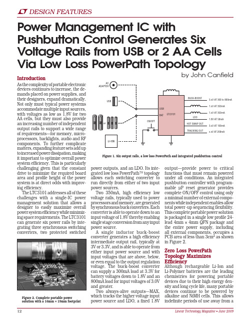
power outputs, and an LDO. Its inte-grated low loss PowerPath™ topology allows each switching converter to run directly from either of two input power sources.Two 350mA, high efficiency low voltage rails, typically used to power processors and memory, are generated by synchronous buck converters. Each converter is able to operate down to an input voltage of 1.8V thereby enabling single stage conversion from any input power source.A single inductor buck-boost converter generates a high efficiency intermediate output rail, typically at 3V or 3.3V, and is able to operate from either input power source and with input voltages that are above, below, or even equal to the output regulation voltage. The buck-boost converter can supply a 300mA load at 3.3V for battery voltages down to 1.8V and an 800mA load for input voltages of 3.0V and greater.Two always-alive outputs—MAX, which tracks the higher voltage input power source and LDO, a fixed 1.8VIntroductionAs the complexity of portable electronic devices continues to increase, the de-mands placed on power supplies, and their designers, expand dramatically. Not only must typical power systems accommodate multiple input sources, with voltages as low as 1.8V for two AA cells, but they must also provide an increasing number of independent output rails to support a wide range of requirements—for memory, micro-processors, backlights, audio and RF components. To further complicate matters, expanding feature sets add up to increased power dissipation, making it important to optimize overall power system efficiency. This is particularly challenging given that the constant drive to minimize the required board area and profile height of the power system is at direct odds with improv-ing efficiency.The LTC3101 addresses all of these challenges with a single-IC power management solution that allows a designer to easily maximize overall power system efficiency while minimiz-ing space requirements. The LTC3101 can generate six power rails by inte-grating three synchronous switching converters, two protected switchedPower Management IC withPushbutton Control Generates Six Voltage Rails from USB or 2 AA Cells Via Low Loss PowerPath Topologyby John Canfieldoutput—provide power to critical functions that must remain powered under all conditions. An integrated pushbutton controller with program-mable µP reset generator provides complete ON/OFF control using only a minimal number of external compo-nents while independent enables allow total power-up sequencing flexibility. This complete portable power solution is packaged in a single low profile 24-lead 4mm × 4mm QFN package and the entire power supply, including all external components, occupies a PCB area of less than 3cm 2 as shown in Figure 2.Zero Loss PowerPath Topology Maximizes EfficiencyAlthough rechargeable Li-Ion and Li-Polymer batteries are the leading chemistries for powering portable devices due to their high energy den-sity and long cycle life, many portable devices continue to be powered by alkaline and NiMH cells. This allowsindefinite periods of use away from a3.xV AT 300 to 800mA 1.xV AT 350mA 1.xV AT 350mA1.8V AT 50mA 3.xV AT 100mA x.xV AT 200mAFigure 1. Six output rails, a low loss PowerPath and integrated pushbutton controlFigure 2. Complete portable powersolution with a 16mm × 19mm footprintcharging socket—which is particularly important for devices intended for use in remote locales such as handheld personal navigation devices or portable medical devices. Voice recorders, digi-tal still cameras and ultra-small video recorders are additional examples of devices that benefit from the ability to operate from a pair of commonly avail-able batteries, rather than requiring the lengthy recharging cycle needed for an internal Li-Ion battery.Even in portable devices where the primary power source is restricted to AA or AAA form factor cells, there still exist a wide variety of compat-ible chemistries including alkaline, rechargeable alkaline, NiMH and single-use lithium. As a result, theAA/AAA powered device must accom-modate a wide range of input voltages, from 1.8V for two series alkaline cells near end of life, to approximately 3.7V for a pair of fresh non-rechargeable lithium cells. With its wide 1.8V to 5.5V input voltage range, the LTC3101 can easily support all of these bat-tery chemistries. In addition, the LTC3101 is able to operate from a single standard Li-Ion/Polymer cell in cases where recharging is performed independently.Although rechargeable cells are usually charged outside these types of devices, the power supply must accommodate a secondary tethered power source such as USB or a regu-lated wall adapter. Consequently, the power supply must include a means to generate every power rail from either of two input sources, and the ubiquitous 3.3V rail must be generated from input power sources that can be higher or lower voltage.In many devices, the capability to handle dual power sources is provided by using discrete power MOSFETs to switch regulator inputs between the two input power sources or by utilizing two regulators for generation of each rail (for example, a buck converter that generates a 3.3V rail from the USB input in conjunction with a boost converter that generates the 3.3V rail from the battery input).Both of these approaches suffer from significant drawbacks. The par-allel converter approach increasessystem cost and size given that onlyone converter is ever active at any giventime and often suffers from glitchesand disruptions to the output railsduring the transition between thetwo input power sources. Similarly,the discrete power switch techniquereduces efficiency due to the additionof extra series elements in the powerpath, increases component count,and can also lead to disruptions inthe output rails unless the supplycrossover is carefully controlled.The LTC3101 avoids these prob-lems by using a low loss PowerPathtopology as shown in Figure 4, whereeach converter is able to operate di-rectly from either input power source.In this architecture, each switchingconverter utilizes an additional powerswitch, which is connected to thealternate power input. As a result,each converter is able to run withmaximum efficiency from either inputpower source so no efficiency penaltyis incurred in supporting dual inputpower sources.The total solution area is minimizedby the fact that the same inductor isused in either case. In addition, theautomatic transition between thetwo input power sources is seam-less—there is no interruption to anyof the output rails. Figure 5 shows thetransient response of the buck-boostconverter as the input power sourcetransitions from battery power to USBpower in response to a live cable pluginto a USB port.Integrated Buck-BoostProvides High Efficiency3V/3.3V Rail fromAny Power SourceIn many portable devices an intermedi-ate supply rail, typically regulated to3.3V, is required to power an RF stageor audio amplifiers. Often this rail isgenerated from the two series AA cellsusing a boost converter. However, thehigher cell voltage of single-use lithiumIN ≥ 1.8VIN ≥ 3V1.8V AT 50mAV OUT21.8V350mAV OUT11.5V350mAFigure 3. Typical applicationV OUTUSBBAT BUCK-BOOSTV OUTFigure 4. The low loss PowerPath architectureMAX and Hot Swap Outputs Power Additional Regulators and Flash Memory CardsPortable electronic devices often re-quire additional miscellaneous power supplies, such as current regulated drivers for LED backlighting and LDOs for low power rails. Typically these secondary supplies must be functional whenever either input power source is present, so they also require power path control to switch between the two input power sources.External supplies can take ad-vantage of the LTC3101’s PowerPath control circuit via the MAX output, which continuously tracks the higher voltage input power source. Additional regulators can be directly connected to this output, thus freeing the de-signer from the need to implement an additional switched power path. The MAX output is able to support a 200mA load and is current limited to protect against overload conditions and short circuits.Many portable electronic devices provide flash memory card inter-faces for use as bulk storage memory. Typical flash memory cards such as Compact Flash (CF) and Secure Digi-tal (SD) formats require a regulated 3.3V supply that is typically capable of providing tens of milliamps. How-ever, many flash memory cards have a significant amount of supply bypass capacitance installed on the card and when hot plugged into a live 3.3V rail, the inrush current required to charge these supply bypass capacitors on the memory card can momentarily drag down the host’s supply, caus-ing disruption to other ICs powered by that rail.batteries such as the Energizer e 2 brand can cause problems when the battery voltage is significantly higher than the output voltage. Depending on the boost converter utilized, this can result in low efficiency operation or even loss of regulation on the 3.3V rail.To avoid this problem, the LTC3101 generates the 3.3V rail utilizing a buck-boost converter, which accepts any input voltage in the range 1.8V to 5.5V without sacrificing efficiency. In fact, when operating with a fresh pair of single-use lithium batteries at 3.7V, the LTC3101 buck-boost efficiency is greater than 94% at 150mA load cur-rent. In addition, the same buck-boost converter is able to operate directly from the USB input, so generation of the 3.3V rail requires only a single inductor.Reverse Blocking LDO Enables Data Retention During Battery SwapsMany portable electronic devices con-tain critical circuitry such as real time clocks, which must remain powered under all conditions. The MAX and LDO outputs of the LTC3101 are alive as long as either input power source is present, regardless of the state of the pushbutton interface or enable inputs. It is also possible to connect a large capacitor directly to the LDO output to serve as a charge reservoir for powering critical functions during times, such as battery swaps, when both input power sources are tempo-rarily removed. In its reverse blocking state, the maximum reverse current through the LDO is limited to under 1µA in order to preserve charge in the reservoir capacitor.The LTC3101’s dedicated 100mA hot swap output (powered from the buck-boost converter rail) does not have this problem. The independent current limit of the hot swap switch allows flash memory cards to be hot plugged without disruption to the primary 3.3V rail. In addition, the hot swap output is fully short circuit protected to safeguard against ac-cidental shorts at the memory card interface port.Low Quiescent Current Minimizes Battery DrainMost portable electronic devices spend significant, if not the majority, of their time in sleep or standby modes. In fact, even when an appliance is off, there is often circuitry that must remain pow-ered, including real time clocks and volatile memory storing configuration settings. The always-alive 1.8V LDO and tracking MAX outputs remain powered whenever either input power source is present allowing them to be utilized for supplying such critical functions. In order to minimize battery discharge during this time, the total quiescent current draw of the LTC3101 with both the MAX and LDO outputs active is reduced to 15µA.Many portable electronic devices also support a standby mode in which several of the system’s voltage rails must be kept in regulation. Typically, in standby the microprocessor and memory remain powered and the processor is placed in a low current sleep mode enabling the device to re-turn to an active operating state with minimal delay.In order to minimize battery drain in such modes of operation, all three switching converters in the LTC3101 feature Burst Mode operation, which can be enabled via a dedicated pin. With Burst Mode operation enabled, the buck converters automatically transition from PWM to Burst Mode operation at sufficiently light load (typically 10mA) while the buck-boost converter uses Burst Mode operation at all load currents. In Burst Mode operation with all six output rails maintained in regulation the total quiescent current draw of the LTC3101OUTPUT VOL TAGE 200mV/DIVINDUCTOR CURRENT 200mA/DIV V USB 2V/DIV100µs/DIVFigure 5. Buck-boost output voltage transient on USB hot plugis reduced to only 38µA. In addition, to ensure low supply rail noise, the Burst Mode operation output voltage ripple is typically less than 1% of the regulation voltage of each output rail. All three switching converters can be forced into fixed frequency PWM mode operation to ensure low noise opera-tion while critical system functions are underway.Flexible Power-Up Sequencing OptionsThe LTC3101 provides a variety of sequencing options. Most systems that incorporate multiple power supply rails require that they come into regulation in a certain sequence with specific timing. This is because individual ICs and modules that are powered from multiple rails need particular sequencing to minimize start-up current and ensure predict-able power-up behavior.Common examples include micro-processors and FPGAs, which often require that the peripheral supply powering the I/O buffers is made available only after the lower voltage core is in regulation. In addition, at the board level, many systems bring up the supplies for peripheral devices only after the processor is powered up to avoid erratic behavior from peripher-als lacking processor oversight.Each switching converter in the LTC3101 has an internal power-good comparator, which is used internally to sense when that rail is in regula-tion. The default power-up sequence enables the individual outputs in the following order: buck converter 1, buck converter 2, buck-boost converter, and finally the hot swap output. Each converter is enabled once the preced-ing converter in the sequence reachesregulation (typically 94% of the target output voltage). The default power-up sequence using all converter channels is shown in Figure 6.If the dedicated enable pin for any switching converter is held low during the pushbutton triggered initiation, that converter is simply skipped in the default power-up sequence, but that channel can still be enabled at a later time. This functionality allows the LTC3101 to implement any arbitrary power-up sequence using few if any external components.For example, in some systems the 3.3V buck-boost rail must come up first, followed by both buck rails in unison. This can be accomplished by driving the buck enables from the hot swap output, HSO, as shown in Figure 7. The bucks do not power up in the normal sequence since their enables are low to start. Once the buck-boost reaches regulation, the hot swap output is enabled, which in turn enables the two buck converters. Since the hot swap output is not powered until the buck-boost is in regulation, this configuration ensures that the buck converters do not become active until after the buck-boost is in regula-tion, as shown by the waveforms in Figure 8.If an additional delay is required before the bucks are enabled, thiscan be accomplished by adding a simple RC filter with the desired time constant between the hot swap output and the buck enables. Notice however, that if the hot swap output is forced to ground, the buck converters will be disabled. If there is a potential for the hot swap output to fall below the enable threshold (typically 0.7V) dur-ing normal operation, then the buck enables can instead be driven through an RC delay from the buck-boost volt-age directly rather than from the hot swap output.ConclusionThe LTC3101 is perfectly suited for the needs of the next generation of extended functionality compact por-table electronic devices.The job of the power system designer is simplified by its compact solution footprint and ability to generate six commonly required output voltage rails automatically from two indepen-dent wide input voltage range power sources. The LTC3101’s low quiescent current and a high efficiency, low loss PowerPath architecture maximize battery life. A wide range of output voltages, programmable duration µP reset generator, and independent enables offer flexibility and easy cus-tomization. LFigure 7. Sequencing the buck enables using the hot swap output rail500µs/DIVV OUT BUCK 1(1V/DIV)V OUT BUCK 2(1V/DIV)V OUT BUCK-BOOST(2V/DIV)HOT SWAP (2V/DIV)Figure 8. Power-up sequencing, buck-boost followed by the buck outputs500µs/DIVV OUT BUCK 1(1V/DIV)V OUT BUCK 2(1V/DIV)V OUT BUCK-BOOST(2V/DIV)HOT SWAP (2V/DIV)Figure 6. Default power-up sequencing。
基于压电能量收集技术的自供电电源设计

基于压电能量收集技术的自供电电源设计陈志敏;荣训;曹广忠【摘要】针对环境和工业检测领域小型无线传感器网络节点的供电问题,提出了一种基于压电能量收集技术的自供电电源设计方案.利用压电能量收集器将机械振动能转换为电能,基于LTC3588-1电源管理芯片搭建电压变换及能量存储电路,获得可供传感器工作的直流电源.实验结果表明,设计的基于压电能量收集技术的自供电电源可为低功耗无线传感器网络节点提供电能,具有应用前景.【期刊名称】《电子设计工程》【年(卷),期】2016(024)010【总页数】3页(P105-107)【关键词】压电能量收集技术;无线传感器网络节点;能量收集电路;自供电【作者】陈志敏;荣训;曹广忠【作者单位】深圳大学机电与控制工程学院深圳电磁控制重点实验室,广东深圳518060;深圳大学机电与控制工程学院深圳电磁控制重点实验室,广东深圳518060;深圳大学机电与控制工程学院深圳电磁控制重点实验室,广东深圳518060【正文语种】中文【中图分类】TN712.5微机电系统和低能耗嵌入式系统的飞速发展,使得无线传感器网络技术应运而生。
无线传感器网络节点是无线传感器网络的基本功能单元,通常是带有传感器和无线收发器的微机系统,可用于测量环境中的多种参量,包括温度、压力、湿度、日射率以及复杂的图像、音频和视频等。
目前,无线传感器网络应用集中在环境和工业检测领域,间隔数秒或数小时的检测结果反映了某一过程或现象的时间变化规律。
传感器的节点分布众多,无线传感器网络中的节点一般用电池供电,可使用的电量非常有限,并且对于有成千上万节点的无线传感器网络来说,更换电池非常困难,甚至是不可能的。
因此,为无线传感器网络节点的寻找替代化学电池的自供电电源可以有效解决这些问题。
通常,这些节点具有以下特征[1]:1)具有较低占空比。
2)休眠状态时具有较低功率(10~300 μW)。
3)工作状态(轮询、发送、接收)具有较高功率,一般在500 μW到600 μW之间,如果包括无线收发单元在内,最终的功率通常在2 mW到3 mW之间。
LTC1760的双电池充电系统设计
LTC1760充电电路设计智能电池系统管理电路实现直流输入与智能电池组输入之间、两个智能电池组之间的电源路径选择,智能电池组的充电管理以及与主机系统之间的通信交互功能。
选用Linear Technology公司的双智能电池管理器芯片LTC1760作为智能电池系统管理电路的核心。
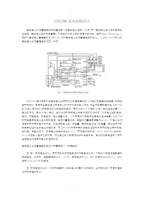
以LTC1760为核心的智能电池系统管理电路如图3所示。
LTC1760是为使用双路智能电池应用而设计的高度集成的3级电池充电器和选择器,采用降压开关拓扑,具有符合智能电池标准定义的多种功能和输入限流、安全限制等新增功能。
LTC1760的SMBus接口可以跟踪电池的内部电压和电流,同时允许一个外接的SMBus主机监控任意一个电池的状态。
通过SMBus接口,主机系统可获知电池供电系统的工作状态,例如电池组的电压、电流、充电电压、充电电流、电池告警状态,以及使用的外接电源还是电池组供电等。
LTC1760的充电精度由电池组内部的电压、电流测量值决定,典型的测量精度误差为±0.2%。
双电池系统通常采用顺序放电方式放电,即先消耗电池组1的电量,再消耗电池组2的电量,通过这种方式来简单地延长总的电池放电时间。
而LTC1760采用专有的供电路径架构支持两路电池同时充电或放电。
典型状态下,可使电池供电时间延长10%,而充电时间可减少50%。
LTC1760能够在10 μs内在输入电源之间切换,防止电池或外部电源迁移时供电中断。
电池的热敏电阻可以用于监控电池的温度和电池的连接状态智能电池系统管理电路在设计中需确定5个关键参数:①输入限流电阻RCL。
用于限制系统充电电流和负载电流之和,不超过外接电源适配器的额定电流。
系统中,适配器选择24 V、150 W,额定电流为6 A,RCL的电流ILIM=5.7 A,RCL 选择0.018 Ω/1 W的电阻。
②限流电阻RILIM。
设定充电器可以供给电池的最大允许电流,任何超过这个限度的值都会被限定值所取代。
- 1、下载文档前请自行甄别文档内容的完整性,平台不提供额外的编辑、内容补充、找答案等附加服务。
- 2、"仅部分预览"的文档,不可在线预览部分如存在完整性等问题,可反馈申请退款(可完整预览的文档不适用该条件!)。
- 3、如文档侵犯您的权益,请联系客服反馈,我们会尽快为您处理(人工客服工作时间:9:00-18:30)。
Linear LTC3588-1压电能量收集电源方案
关键字:电源管理,能量收集器,DC/DC转换器Linear 公司的LTC3588-1是压电能量收集电源,集成了低噪音全波整流和高效降压转换器,组成完整的能量收集解决方案,最适合高输出阻抗的能量源如压电传感器.输入电压2.7V-20V,输出电流高达100mA,可选输出电压1.8V, 2.5V, 3.3V和3.6V,可用于压电能量收集,电-机械能量收集,无线HVAC传感器,轮胎压里传感器,遥控光开关,毫微瓦降压稳压器.本文介绍LTC3588-1主要特性,方框图以及多种应用电路图,包括
100mA压电能量收集电源电路图, 最小尺寸的1.8V低压输入压电能量收集电源电路图, 电场能量和热电能量收集器电路图等.
LTC3588-1: Piezoelectric Energy Harvesting Power Supply
The LTC.3588-1 integrates a low-loss full-wave bridge rectifier with a high efficiency buck converter to form a complete energy harvesting solution optimized for high output impedance energy sources such as piezoelectric transducers. An ultralow quiescent current
undervoltage lockout (UVLO) mode with a wide hysteresis window allows charge to accumulate on an input capacitor until the buck converter can effi ciently transfer a portion of the stored charge to the output. In regulation, the LTC3588-1 enters a sleep state in which both input and output quiescent currents are minimal. The buck converter turns on and off as needed to maintain regulation.
Four output voltages, 1.8V, 2.5V, 3.3V and 3.6V, are pin selectable with up to 100mA of continuous output current; however, the output capacitor may be sized to service a higher output current burst. An input protective shunt set at 20V enables greater energy storage for a given amount of input capacitance.
LTC3588-1主要特性:
950nA Input Quiescent Current (Output in Regulation – No Load)
450nA Input Quiescent Current in UVLO
2.7V to 20V Input Operating Range
Integrated Low-Loss Full-Wave Bridge Rectifier
Up to 100mA of Output Current
Selectable Output Voltages of 1.8V, 2.5V, 3.3V, 3.6V High Efficiency Integrated Hysteretic Buck DC/DC
Input Protective Shunt – Up to 25mA Pull-Down at VIN ≥ 20V
Wide Input Undervoltage Lockout (UVLO) Range
Available in 10-Lead MSE and 3mm x3mm DFN Packages
LTC3588-1应用:
Piezoelectric Energy Harvesting
Electro-Mechanical Energy Harvesting Wireless HVAC Sensors
Mobile Asset Tracking
Tire Pressure Sensors
Battery Replacement for Industrial Sensors Remote Light Switches
Standalone Nanopower Buck Regulator
图1.LTC3588-1方框图
图2.LTC3588-1 100mA压电能量收集电源电路图
图3.LTC3588-1 3.3V压电能量收集电源电路图:给带无线发送器的微处理器和50mA瞬态负载供电.
图4.最小尺寸的1.8V低压输入压电能量收集电源电路图
图5.采用单个压电晶体和自动加电次序的双电源电路图
图6.带备份电池的压电能量收集器电路图
图7.AC火线供电的3.6V降压稳压器,大输出电容支持重负载
图8.电场能量收集器电路图
图9.5-16V太阳能供电的2.5V电源,其超大电容增加输出能量存储和备份电池
图10.热电能量收集器电路图。
