Bourns 3296W P-1-203多圈电位器
可调电位器型号

最小阻抗
22Ω
最大阻抗
47K
阻值误差
±5%/±10%
额定功率(W)
5
旋转角度
300°
旋转寿命(无负载)
10000周
封装直径(mm)
45
形状
圆形
转数
1
密封型
接线端
接线片焊接
输出特性-线性
X
线性度
±5%~±10%
最小阻抗
22Ω
最大阻抗
47K
阻值误差
±5%/±10%
额定功率(W)
3
旋转角度
300°
旋转寿命(无负载)
10000周
轴
金属
电阻材料
碳膜
接线端
接线片焊接
输出特性-线性
X
线性度
±5%~±10%
最小阻抗
22Ω
最大阻抗
47K
阻值误差
±5%/±10%
额定功率(W)
5
旋转角度
270°
旋转寿命(无负载)
10000周
封装直径(mm)
45
形状
圆形
转数
1
密封型
IP40
轴
金属
电阻材料
线绕
接线端
接线片焊接
输出特性-线性
ALPS马达驱动型电位器RK168系列选型手册

金属轴 绝缘轴 旋钮操作型 中空轴
总阻值种类
总阻值 (kΩ)
电阻规律
电阻规律
操作部的种类
10
20
15A
L1 12
˃
ø6 4.5
C1
50
3B
L1 20 25 30
工作最大 电流值
旋转时 100mA 末端空转时 150mA (4.5V DC)
100
Unit:mm
轴承和支架固定标准尺寸
7
Unit:mm
旋转电位器 滑动电位器
金属轴
产品一览
电阻体数 安装方向
操作部 操作部长度 总阻值
形状
(L1)(mm)
(kΩ)
电阻规律
马达 配线端子
最小订货单位 (pcs.) 日本 出口
产品编号
图号
2联
3B
有
RK16812MG099 1
Horizontal type
平轴
25
100
200
200
4联
15A
无
RK16814MGA0K 2
适用于相互偏差
(2 联以上的音量用)
-40dB to 0dB 3dB max.
-
-70dB to -60dBɹ3dB max. -60dB to 0dBɹ2dB max
-100dB to 0dB 2dB max.
-60dB to -40dBɹ5dB max. -40dB to 0dBɹ3dB max.
轴的形状
齿轴, 平轴, 槽轴
平轴
槽轴, 平轴
槽轴
平轴
端子形状
插入式, 引线
插入式
附属开关
-
按开开关
PRO16-III抄控器功能及使用说明书

PRO16-III抄控器功能及使用说明青岛东软载波科技股份有限公司1.用途及使用范围PRO16-III型抄控器和掌上电脑或计算机、载波表一起构成了EASTSOFT®远程集中抄表系统(AMR)的主动发送设备,实现载波通信功能,利用低压电力线为通信介质与终端设备(载波电能表)建立可靠的数据连接,并以半双工的通信方式对终端设备进行抄控操作。
主要应用在集抄系统的现场安装、生产调试等环节。
2.功能及特点PRO16-III型抄控器采用东软公司自主研制开发的低压电力线载波通信发送芯片PLCi38-III,数据链路层采用高级数据链路控制协议,应用层兼容DL/T645—2007规约。
PRO16-III型抄控器和掌上电脑或计算机配合使用能完成以下功能:●设置参数:通过电力线设置和修改载波电表参数。
●抄读参数:具有指定抄读一只电表数据:表号、初始电量、初始密码等●监控单表:可以对单表进行实时监控其主要特点是:数据传输可靠,抗干扰能力强,外形小巧便于携带,是实现场维护不可缺少的必要设备。
3.工作原理及结构3.1.结构图3.2.工作原理抄控器通过RS232串行口或USB口接收主站(手持设备或计算机)的抄控命令,经载波芯片PLCi38-III扩频调制、发射馈网电路选频放大后,传送到低压电力线上;电力线终端设备(载波电能表)收到命令后向抄控器返回应答,通过RS232串行口或USB 实现通信。
4.规格和主要的技术参数5.抄控器通讯说明5.1.掌机软件版本1.支持规约类型:DL/T645-1997通讯协议、DL/T645-2007通讯协议;2.软件下载方式:登陆东软网站/选择‘技术支持’,在‘掌机软件’栏里有各版本程序的下载链接;3.具体抄读电表类型与版本的对应关系如下:5.2. 连接PC 机通讯5.2.1.通讯连接示意图注意:A/B 接线图1 基本测试使用图2 测试通讯效果5.2.2. 通讯软件说明1. 支持规约类型:DL/T645-1997通讯协议、DL/T645-2007通讯协议;2. 软件下载方式:登陆东软网站/选择‘技术支持’,在‘软件及文档下载’调试软件栏里有“DL/T645 - 1997协议调试器(V2.13)”和“DL/T645 - 2007协议调试器”的下载;3. 以下以DL/T645 - 1997协议调试器(V2.13)软件为例说明使用方法 a) 运行参数设定软件运行后首先显示如下参数界面:可以指定串口参数,如左图所示;切换到电表参数页面中可以设定电表的通讯密码等参数,电表参数中的“电表密码”项目即07-645规约中的02级密码,电表参数中的“低级密码”项目即07-645规约中的04级密码b)电表数据项单项操作在如下主界面中,录入表号以后,可以选择操作的控制码,如读数据、写数据、广播校时、冻结命令、电表清零等如果选择的是读数据和写数据,需要填写数据标识内容,也可以点击数据标识来进行数据项选择,弹出如下界面,从中可以选择需要操作的数据项目选择完毕,即可点击发送按钮来执行电表操作,在消息栏目中可以看到软件与电表的交互报文,在状态栏中可以看到返回报文的数据体内容,下图所示的是抄读电表“800000000001”的“00010000当前正向有功总电量”数据,返回的数据内容是00008463,参照规约解析是84.63kWh注意事项:✧通讯速率:9600bps,数据位:8位,停止位:1位,校验方式:偶校验;✧如果需要对电表进行设置,需要输入8位电表密码(6位密码加2位权限);✧如果采用采集器方式对电表通讯,根据需要选中“通过采集器进行抄读”,并正确输入采集器地址;✧如有需要需要选中“命令帧前使用前导符”按钮,同时前导符输入:FC,次数为:1;以上设置完成后,打开串口,退回到主界面,输入表号,然后选择通讯类型以及数据标识,进行通讯即可;详细的通讯收发报文将会在窗体空白出显示;关于该软件详细的说明,参见软件包中的用户手册。
MAX25600 高压电压高明亮 LED(HB LED)槽桩控制器评估套件说明书

MAX25600EVKIT#Evaluates: MAX25600 MAX25600 Evaluation KitGeneral DescriptionThe MAX25600 evaluation kit (EV kit) provides a proven design to evaluate the MAX25600 automotive high-volt-age, high-brightness LED (HB LED) buck boost controller. The EV kit operates from 8V to 48V DC supply voltage. The EV kit is configured to deliver up to 1.5A to one string of one to fifteen LEDs. The total voltage of the string can vary from 3V to 60V. The anode of the LED string should go to LED+ terminal and the cathode to the LED- terminal. Benefits and Features●8V to 48V Input Voltage Range●Demonstrates Analog Dimming Control, DigitalDimming Control●Demonstrates Input Current Limit●Demonstrates LED Current Monitoring function●Demonstrates LED Short and Open Protection●Proven PCB Layout●Fully Assembled and TestedOrdering Information appears at end of data sheet.Quick StartRequired Equipment●MAX25600 EV kit●12V, 5A DC power supply● A series-connected LED string rated at least 1.5A●Oscilloscope with a current probeProcedureThe EV kit is fully assembled and tested. Follow the steps below to verify board operation:Caution: Do not turn on the power supply until all connections are made.1) Verify that all jumpers are in their default positions,as shown in Table 1.2) Connect the positive terminal of the 12V supply tothe VINP1 board PCB pad and the negative terminal to the GND1_board PCB pad.3) Connect the LED string across the LED+ and LED-PCB pads on the EV kit. The Anode of the LEDstring should go to the LED+ PCB pad and Cathode of the LED string to LED- PCB pad.4) Clip the current probe on the wire connected to theLED string.5) Turn on the DC power supply.6) Verify that the LEDs turn on.7) Verify that the oscilloscope displays approximately1.5A.Click here for production status of specific part numbers.PRELIMINARYEvaluates: MAX25600MAX25600 Evaluation Kit Detailed DescriptionThe MAX25600 evaluation kit (EV kit) provides a proven design to evaluate the MAX25600 automotive high-volt-age, high-brightness LED (HB LED) buck boost controller. The EV kit operates from 8V to 48V DC supply voltage. The EV kit is configured to deliver up to 1.5A to one string of LEDs. The total voltage of the string can vary from 3V to 60V. The anode of the LED string should go to LED+ terminal and the cathode to the LED- terminal.Analog Dimming Control (ICTRL)When J2 is closed, the LED current is set by resistive divider from VCC. The equation to set the LED current isICTRLLED V 200mVI 5R9−=×In the case of the EV kit, ILED is set to 1.5A. Use a screw driver on the potentiometer R21 to adjust the LED current.PWM DimmingThe EV kit demonstrates the PWM dimming feature of the MAX25600 using either an external PWM signal, or a DC voltage at the PWMDIM pin.External PWM dimming:Keep J4 open and remove the 0.1uF C55 capacitor (installed by default). Connect an external PWM signal to the PWMDIM test point. Vary the duty cycle to increase or decrease the intensity of the HB LED string. The PWMDIM input of the device has a 2V (max) rising thresh-old and a 0.4V (min) falling threshold and is compatible with 3.3V and 5V logic-level signals.Analog-to-PWM dimming:Keep J4 open and keep the 0.1uF C55 (installed by default). The PWM dimming duty cycle is set by the volt-age at PWMDIM between 0.2V (0% duty) and 3.2V (100% duty). Drive the PWMDIM test point with an external DC source. PWMDIM voltages above 3.2V set the dimming duty cycle to 100%.Table 1. MAX25600 EV Kit Jumper DescriptionsJUMPE R SHUNT POSITIONDESCRIPTIONJ1Closed Short the PMOS PWM dimming switch.Open*PWM Dimming done with the PMOS switchJ2Closed Uses the resistive divider from VCC and the potentiometer R21 to set the LED current.Open Apply an external dc voltage between 0.2V to 1.2V for setting LED current.J3OpenConnect an external power supply for the IN pin of the IC using the IN_IC PAD.1-2*Connects the IN input of the IC to the VIN power supply connected on VINP1 PAD.2-3The IN and VCC inputs of the IC are shorted and should be driven with an external 5V supply.J4OpenApply an external PWM clock source for PWM dimming or apply an external dc source between 0.2V to 3.2V for analog PWM dimming.1-2*PWMDIM pin pulled to VCC for 100% duty.2-3PWMDIM pin pulled to GND to turn OFF.PRELIMINARYEvaluates: MAX25600MAX25600 Evaluation Kit Current Monitor OutputThe EV kit also demonstrates the current-monitor out-put feature of the buck boost controller. The MAX25600 includes a current monitor on the IOUTV pin. The IOUTV voltage is an analog voltage indication of the LED current when DIM is high. The voltage on the IOUTV pin is given by the following equation:V IOUTV = I LED x R CS_LED x 5 + 0.2VInput-Current LimitThe MAX25600 features circuitry that limits the input cur-rent during line dropouts. Refer to the IC datasheet for details on setting the input current limit.External VCC inputThe EV kit demonstrates operation of the buck boost con-troller with an external VCC input. In this case, the internal LDO is not used. Move the shunt to pins 2-3 on J3 (the IN and VCC pins of the buck controller are shorted together). Apply an external power supply between 4.6V and 5.5V on the IN_IC PCB pad to allow switching of the device.FaultsOpen and Short LEDs:The IC detects the open and short fault conditions of the LEDs and the fault pin is pulled low. The fault pin also goes low when there is an overtemperature condition. The fault pin is an open-drain output and is active low.#Denotes RoHS compliant.PART TYPE MAX25600EVKIT#EV KitOrdering InformationPRELIMINARYEvaluates: MAX25600 MAX25600 Evaluation KitMAX25600 EV Kit Bill of MaterialsITEM QTY REF DES MFG PART #MANUFACTURER VALUE DESCRIPTION19AGND, ICTRL, IN_IC, LED+,LED-, PGND, PGND1,PWMDIM, VINP19020 BUSS WEICO WIRE MAXIMPAD EVK KIT PARTS; MAXIM PAD; WIRE; NATURAL;SOLID; WEICO WIRE; SOFT DRAWN BUS TYPE-S; 20AWG26C1, C4, C20, C22,C24, C55885012206071;CGJ3E2X7R1E104K080AA;C1608X7R1E104K080AA;C0603C104K3RAC;GRM188R71E104KA01;C1608X7R1E104KWURTH ELECTRONICS INC;TDK;TDK;KEMET0.1UFCAPACITOR; SMT; 0603; CERAMIC; 0.1uF; 25V;10%; X7R; -55degC to + 125degC; +/-15% from -55degC to+125degC39C2, C3, C6, C7, C9,C10, C12, C13, C15CGA6M3X7S2A475K200AE;CGA6M3X7S2A475K200ABTDK;TDK 4.7UF CAPACITOR; SMT (1210); CERAMIC CHIP; 4.7UF;100V; TOL=10%; TG=-55 DEGC TO +125 DEGC; TC=X7S; AUTO41C5CGA3E3X7S2A104K080AB TDK0.1UF CAPACITOR; SMT (0603); CERAMIC CHIP; 0.1UF;100V; TOL=10%; TG=-55 DEGC TO +125 DEGC; TC=X7S53C8, C14, C21CC0603KRX7R0BB104;GRM188R72A104KA35;GCJ188R72A104KA01;HMK107B7104KA;06031C104KAT2AYAGEO;MURATA;MURATA;TAIYO YUDEN;AVX0.1UF CAPACITOR; SMT (0603); CERAMIC CHIP; 0.1UF;100V; TOL=10%; TG=-55 DEGC TO +125 DEGC; TC=X7R61C11EEV-FK2A680Q PANASONIC68UF CAPACITOR; SMT (CASE_H13); ALUMINUM-ELECTROLYTIC; 68UF; 100V; TOL=20%; MODEL=EEV SERIES71C17C0603C471K1RAC; 06031C471KAT2A KEMET;AVX470PF CAPACITOR; SMT; 0603; CERAMIC; 470pF; 100V;10%; X7R; -55degC to + 125degC; +/-15% from -55degC to +125degC81C18C0603X5R160-105KNP;EMK107BJ105KA;C1608X5R1C105K080AA;GRM188R61C105K;0603YD105KAT2A;CL10A105KO8NNNVENKEL LTD.;TAIYO YUDEN;TDK;MURATA;AVX;SAMSUNGELECTRO-MECHANICS1UFCAPACITOR; SMT; 0603; CERAMIC; 1uF; 16V;10%; X5R; -55degC to + 85degC; 0 +/-15% degC E 20-0001u-63 FOR NEW DESIGN91C19C1608C0G1E103J080AA TDK0.01UF CAPACITOR; SMT (0603); CERAMIC CHIP;0.01UF; 25V; TOL=5%; MODEL=; TG=-55 DEGC TO +125 DEGC; TC=C0G101C23C1608X5R1E225K;TMK107ABJ225KA;TMK107BJ225KA;GRM188R61E225KA12TDK;TAIYO YUDEN;TAIYO YUDEN;MURATA2.2UF CAPACITOR; SMT (0603); CERAMIC CHIP; 2.2UF;25V; TOL=10%; MODEL=; TG=-55 DEGC TO +85 DEGC; TC=X5R111C25C0603H102J1GAC KEMET1000PF CAPACITOR; SMT (0603); CERAMIC CHIP; 1000PF;100V; TOL=5%; MODEL=HT SERIES; TG=-55 DEGC TO +200 DEGC; TC=C0G121C51CGA3E2X8R1E104K080AE TDK0.1UF CAP; SMT (0603); 0.1UF; 10%; 25V; X8R;CERAMIC CHIP134D1, D2, D5, D61N4148W-7-F DIODES INCORPORATED1N4148W-7-F DIODE; SWT; SMT (SOD-123); PIV=100V; IF=0.3A;-65 DEGC TO +150 DEGC142D7, D8BAT46WJ NXP BAT46WJ,115DIODE; SCH; SMT (SOD-323F); PIV=100V; IF=0.25A151FB1HF70ACB322513TDK52INDUCTOR; SMT (1210); FERRITE-BEAD; 52;TOL=+/-25%; 0.4A; -40 DEGC TO +125 DEGC163FLTB, IOUTV, VCC5007KEYSTONE N/A TEST POINT; PIN DIA=0.125IN; TOTAL LENGTH=0.35IN; BOARD HOLE=0.063IN; WHITE; PHOSPHOR BRONZE WIRE SILVER PLATE FINISH;172J1, J2PCC02SAAN SULLINS PCC02SAAN CONNECTOR; MALE; THROUGH HOLE;BREAKAWAY; STRAIGHT THROUGH; 2PINS; -65 DEGC TO +125 DEGC182J3, J4PCC03SAAN SULLINS PCC03SAAN CONNECTOR; MALE; THROUGH HOLE;BREAKAWAY; STRAIGHT THROUGH; 3PINS; -65 DEGC TO +125 DEGC191L1MSS1278-103ML COILCRAFT10UH INDUCTOR; SMT; FERRITE CORE; 10UH; TOL=+/-20%; 5.7A 201L2MSS1278T-472ML COILCRAFT 4.7UH INDUCTOR; SMT; FERRITE BOBBIN CORE;4.7UH; TOL=+/-0.2; 6.2A; -40 DEGC TO +125 DEGC212Q1, Q3SQJA84EP-T1_GE3VISHAY SILICONIX SQJA84EP-T1_GE3TRAN; AUTOMOTIVE N-CHANNEL MOSFET ;NCH; SO-8L; PD-(55W); I-(46A); V-(80V)221Q2BUK9Y72-80E NEXPERIA BUK9Y72-80E TRAN; N-CH LOGIC LEVEL MOSFET ; NCH;LFPAK; PD-(45W); I-(15A); V-(80V)231Q4BUK9Y25-80E NEXPERIA BUK9Y25-80E TRAN; N-CH LOGIC LEVEL MOSFET ; NCH;LFPAK; PD-(95W); I-(37A); V-(80V)241Q5SI7415DN-T1-GE3VISHAY SILICONIX SI7415DN-T1-GE3TRAN; P-CHANNEL 60-V (D-S) MOSFET; PCH;POWERPAK1212-8; PD-(3.8W); I-(-5.7A); V-(-60V)2510R1, R3, R4, R6-R8,R13, R25, R27, R28CRCW06030000Z0VISHAY DALE0RESISTOR; 0603; 0 OHM; 0%; JUMPER; 0.1W; THICK FILM 262R2, R12CRCW06035R62FK VISHAY DALE 5.62RESISTOR; 0603; 5.62 OHM; 1%; 100PPM; 0.10W; THICK FILM 275R5, R11, R17, R19, R20301-10K-RC XICON10K RESISTOR, 0603, 10K OHM, 5%, 200PPM, 1/16W, THICK FILM 281R9CSR1206FTR130STACKPOLE ELECTRONICS INC0.13RESISTOR; 1206; 0.13 OHM; 1%; 100PPM; 0.5W; THICK FILM 291R10ERJ-3EKF5113PANASONIC511K RESISTOR; 0603; 511K OHM; 1%; 100PPM; 0.1W; THICK FILM 301R16CRCW060354K9FK VISHAY DALE54.9K RES; SMT (0603); 54.9K; 1%; +/-100PPM/DEGC; 0.1W311R18288-0603-49.9K-RC XICON49.9K RESISTOR, 0603, 49.9K OHM, 0.1%, 10PPM, 1/16W, THIN FILM321R213296W-1-103LF BOURNS10K RESISTOR; THROUGH-HOLE-RADIAL LEAD;3296 SERIES; 10K OHM; 10%; 100PPM; 0.5W; SQUARE TRIMMING POTENTIOMETER; 25 TURNS; MOLDER CERAMIC OVER METAL FILM331R22CRCW0603560RFK VISHAY DALE560RESISTOR, 0603, 560 OHM, 1%, 100PPM, 0.10W, THICK FILM341R23RG1608P-101-B;ERA-3YEB101V SUSUMU CO LTD.;PANASONIC100RESISTOR; 0603; 100 OHM; 0.1%; 25PPM; 0.1W; THICK FILM351R24RCS060312R0FK VISHAY DALE12RESISTOR; 0603; 12 OHM; 1%; 100PPM; 0.25W; THICK FILM361R26CRCW060349R9FK VISHAY DALE49.9RESISTOR; 0603; 49.9 OHM; 1%; 100PPM; 0.10W; THICK FILM371R55CRCW08051R00FK VISHAY DALE1RESISTOR; 0805; 1 OHM; 1%; 100PPM; 0.125W; THICK FILM382RN1, RN2ERJ-8BWFR024PANASONIC0.024RES; SMT (1206); 0.024; 1%; +/-150PPM/DEGC; 1W392RS1, RS2TLM2BER012F TE CONNECTIVITY0.012RES; SMT (1206); 0.012; 1%; +/-100PPM/DEGC;0.5W;NOTE:PURCHASE DIRECT FROM THE MANUFACTURER401TP17007KEYSTONE7007CONNECTOR; PANELMOUNT; BINDING POST;STRAIGHT THROUGH; 1PIN; BLACK411TP107006KEYSTONE7006CONNECTOR; PANELMOUNT; BINDING POST;STRAIGHT THROUGH; 1PIN; RED421U1MAX25600MAXIM MAX25600EVKIT PART-IC; MAX25600; QFN28-EP; PACKAGE OUTLINEDRAWING: 21-100130; PACKAGE CODE: T2855+5C431PCB MAX25600MAXIM PCB PCB:MAX25600PRELIMINARYEvaluates: MAX25600 MAX25600 Evaluation KitPRELIMINARYEvaluates: MAX25600MAX25600 Evaluation Kit MAX25600 EV Kit Component Placement Guide—Top SilkscreenMAX25600 EV Kit PCB Layout—Top ViewPRELIMINARYEvaluates: MAX25600MAX25600 Evaluation Kit MAX25600 EV Kit PCB Layout—Internal2MAX25600 EV Kit PCB Layout—Internal3PRELIMINARYEvaluates: MAX25600MAX25600 Evaluation Kit MAX25600 EV Kit PCB Layout—Bottom ViewMAX25600 EV Kit Component Placement Guide—Bottom SilkscreenPRELIMINARYEvaluates: MAX25600 MAX25600 Evaluation KitREVISION NUMBER REVISIONDATEDESCRIPTIONPAGESCHANGED05/19Initial release—Revision HistoryFor pricing, delivery, and ordering information, please visit Maxim Integrated’s online storefront at https:///en/storefront/storefront.html.PRELIMINARYMAX25600EVKIT#。
BOURNS 3680 Family - Precision Potentiometer 说明书
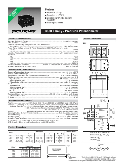
*RoHS Directive 2002/95/EC Jan 27 2003 including AnnexSpecifications are subject to change without notice.Customers should verify actual device performance in their specific applications.Electrical Characteristics 1Standard Resistance Range .............................................................................10 ohms to 1 megohm Total Resistance Tolerance...........................................................................................................±3 %Dielectric Withstanding Voltage (MIL-STD-202, Method 301)Sea Level..........................................................................................................1,000 VAC minimum Power Rating (Voltage Limited By Power Dissipation or 500 VAC, Whichever is Less)+25 °C ...................................................................................................................................2 watts +85 °C......................................................................................................................................0 watt Insulation Resistance (500 VDC)..................................................................1,000 megohms minimum Resolution3681..........................................................................................................................................10 %3682............................................................................................................................................1 %3683.........................................................................................................................................0.1 %3684.......................................................................................................................................0.01 %3685.....................................................................................................................................0.001 %Absolute Minimum Resistance...............................3 ohms or 0.2 % maximum (whichever is greater)Accuracy (Dial Reading to Output Ratio)....................................................................±1.0 % full scaleEnvironmental Characteristics1Operating Temperature Range ...................................................................................-25 °C to +85 °C Storage Temperature Range.......................................................................................-25 °C to +85 °C Temperature Coefficient Over Storage Temperature Range...........................±100 ppm/°C maximum Vibration.........................................................................................................................................10 G Wiper Bounce...........................................................................................0.1 millisecond maximum Total Resistance Shift..............................................................................................±1 % maximum Voltage Ratio Shift................................................................................................±0.2 % maximum Shock.............................................................................................................................................50 G Wiper Bounce...........................................................................................0.1 millisecond maximum Total Resistance Shift..............................................................................................±1 % maximum Voltage Ratio Shift................................................................................................±0.2 % maximum Load Life...............................................................................................................1,000 hours, 2 watts Total Resistance Shift..............................................................................................±2 % maximum Rotational Life.........................................................................75,000 button operations each decade Total Resistance Shift..............................................................................................±2 % maximum IP Rating........................................................................................................................................IP 40Mechanical Characteristics 1Weight....................................3681 (9 gm); 3682 (16 gm); 3683 (23 gm); 3684 (30 gm); 3685 (37 gm)T erminals.....2.79 mm (0.11 in.) wide x .41 mm (.016 in.) thick, tinned solder lugs for 3 #20 AWG wires Soldering Condition........................Recommended hand soldering using Sn95/Ag5 no clean solder,0.025 ” wire diameter. Maximum temperature 399 °C (750 °F) for 3 seconds.No wash process to be used with no clean flux.Marking...............................Manufacturer’s name and part number, resistance value and date code.Ganging (Multiple Section Potentiometers)...............................................Up to 5 decades maximum Readout Marking........................................................................................................10 positions, 0-9Actuating Force...................................................................................19 to 29 oz. on detent decades Actuating Force Variation..............................................................................................4 oz. maximum1At room ambient: +25 °C nominal and 50 % relative humidity nominal, except as noted.NOTE: Terminals 1 & 3 are reversed from illustration for models 3682 and 3684.3680INCR.Product DimensionsDimensionsWeight (Approx.)Model a b c d e –.381 (–.015)oz.gms.368116.51 (.650)14.99 (.590)—9.91 (.39) 4.19 (.165).3369.5368226.67 (1.05)25.15 (.99)10.67 (.42)11.94 (.47)8.38 (.330).57616.5368337.08 (1.46)35.31 (1.39)18.54 (.73)11.94 (.47) 4.19 (.165).82423.5368447.50 (1.87)45.47 (1.79)30.73 (1.21)11.94 (.47)8.38 (.330) 1.07230.5368557.66 (2.270)55.63 (2.190)39.12 (1.540)11.94 (.47)4.19 (.165)1.32037.5DimensionsModel f –.010 (–.254)g –.010 (–.254)368121.08 (.830)15.75 (.620)368221.08 (.830)25.91 (1.020)368321.08 (.830)36.07 (1.420)368421.08 (.830)46.23 (1.820)368521.08 (.830)56.39 (2.220)*Ro H S C O M P L I A N T V E R S I O N S A V A I L A B L ESpecifications are subject to change without notice.Customers should verify actual device performance in their specific applications.Recommended Part NumbersBOLDFACE LISTINGS ARE IN STOCK AND READILY AVAILABLE THROUGH DISTRIBUTION.FOR OTHER OPTIONS CONSULT FACTORY.RoHS IDENTIFIER:L =COMPLIANTBLANK =NON-COMPLIANTREV. 08/06。
电位器3296W规格书.PDF

型號:
Model No.:
3296W-1-500
Ⅰ電器性能
ELECTRICAL CHARACTERISTICS
1.1總阻值
Nominal Resistance
50Ω
1.2阻值誤差
Resistance Tolerance
□±10%
1.3線性
Resistance Taper
直線(B)
Linear (B)
3.1機械強度
Mechanical Strength
電阻體受最小1Kg.壓力不會破裂。
Bakelite Base not to be broken down under a force of1Kg.
Ⅳ氣候特性
CLIMATI CCHARA CTERISTICS
4.1使用溫度
Operating Temp.
品名/Commodity:BURANSPotentiometer
型號/Model No:3296W-50R
3296电位器 功率

3296电位器功率一、引言电位器是一种常用的电阻器件,用于调节电路中的电压或电流。
而3296电位器是一种多圈电位器,其主要特点是具有高精度、高可靠性和较大的额定功率。
本文将介绍3296电位器的基本原理、结构特点以及应用领域。
二、3296电位器的基本原理3296电位器是一种可调电阻器,通过旋转电位器上的旋钮,可以改变电路中的电阻值,从而调节电路的电压或电流。
其基本原理是通过调节电位器上的滑动触点位置,改变电位器两端的电阻长度,从而改变电位器的整体电阻值。
电位器的工作原理主要依靠电阻片和滑动触点的接触方式来实现电阻调节。
3296电位器通常由一个导电材料制成的电阻片和一个与电阻片相贴紧并可以沿电阻片轴向滑动的滑动触点组成。
当滑动触点在电阻片上滑动时,触点与电阻片之间的接触长度就会改变,从而改变整个电位器的电阻值。
三、3296电位器的结构特点1. 外观特点3296电位器外观小巧,通常为圆柱形状,直径约为9.5mm,高度约为10mm。
其外壳材质通常为塑料或金属,具有良好的绝缘性能和机械强度。
2. 电路布局3296电位器的电路布局相对简单,通常由三个引脚组成:中间引脚连接电位器滑动触点,两侧引脚分别连接电阻片两端。
在电路中使用时,根据需要将电路连接到相应的引脚上即可。
3. 额定功率3296电位器的额定功率为0.5W,可以承受较大的功率负荷,因此在一些功率较大的电路中使用较为常见。
4. 高精度3296电位器具有较高的精度,通常为±10%或±20%。
这意味着电位器的实际电阻值与标称电阻值之间的误差在允许范围内,可以满足大多数电路的要求。
四、3296电位器的应用领域由于3296电位器具有高精度和较大的额定功率,因此在许多电子设备中都有广泛的应用。
1. 音频设备3296电位器可以用于调节音频设备中的音量大小,如音响、收音机等。
通过调节电位器的阻值,可以改变信号的幅度,从而控制音量的大小。
2. 显示设备3296电位器可以用于调节显示设备中的对比度、亮度等参数。
MAX3795EVKIT 用户手册说明书
__________________________________________Maxim Integrated Products1 For pricing, delivery, and ordering information, please contact Maxim/Dallas Direct! at 1-888-629-4642, or visit Maxim’s website at .Evaluat es: MAX3795MAX3795 Evaluat ion K it_______________General Desc ript ion The MAX3795 evaluation kit (EV kit) is an assembled demonstration board that provides complete optical and electrical evaluation of the MAX3795 VCSEL driver.The output of the EV kit is interfaced to an SMA connector that can be connected to a 50W terminated oscilloscope. A site for a common cathode VCSEL is provided to allow optical testing._________________________Feat uresFully Assembled and TestedSingle +3.3V Power Supply Operation_______________Ordering Inform at ion PART TEMP RANGE IC-PACKAGE MAX3795EVKIT-40°C to +85°C 24 Thin QFN______________________________________________________________ Com ponent List DESIGNATION QTY DESCRIPTIONC1, C2, C4-C9,C11-C13, C15-C17140.01m F 10% ceramiccapacitor (0402)C310.047m F 10% ceramic capacitor (0402)C101OPENC14110m F ceramic capacitor (0805)C18110m F 10% tantalum capacitor, case BC19, C202OPEN*D11VCSEL laser and photodiode*D21LED, red T1 packageJ1-J77SMA connectors, tab contact, Johnson 142-0701-851JU1-JU7, JU10,JU12-JU13112-pin header, 0.1in centers JU1413-pin header, 0.1in centers None12ShuntsL1-L33Ferrite Bead, Murata BLM18HD102SN1 (0603)L411.2m H inductor (1008LS) Coilcraft 1008CS-122XKBCQ1, Q22NPN transistor (SOT23)Zetex FMMT491A*These components are not supplied but can bepopulated if the user wants to test a VCSEL.DESIGNATION QTY DESCRIPTIONR1, R15250k W variable resistorBourns 3296WR2110k W variable resistorBourns 3296WR14120k W variable resistorBourns 3296WR161500k W variable resistorBourns 3296WR31402W 1% resistor (0402)R41 2.49k W 1% resistor (0402)R5, R122499W 1% resistor (0402R6, R13, R28310.0k W 1% resistor (0402)R7, R102OPEN*R81 4.75k W 1% resistor (0402)R9, R11249.9W 1% resistor (0402)R26110W 1% resistor (0402)R271 1.0k W 1% resistor (0402)R341 1.0k W 1% resistor (0402)R35115k W 1% resistor (0402)R361 1.69k W 1% resistor (0402)R51, R53, R56-574806W 1% resistor (0402)TP1-TP3, TP5TP6-9, TP11-12,TP13-15, TP20-2115Test PointU11MAX3795ETG (24 QFN)U21MAX495 (8 SO)19-0031; Rev 0, 11/04MAX3795 Evaluat ion K it2_________________________________________________________________________________________E v a l u a t e s : M A X 3795__________________Com ponent Suppliers Note: Please indicate that you are using the MAX3795 when contacting these component suppliers.________________________Quic k St artElec t ric al Eval uat i onIn the electrical configuration, an automatic power control (APC) test circuit is included to emulate a semiconductor laser with a monitor photodiode.Monitor diode current is provided by transistor Q1,which is controlled by an operational amplifier (U2).The APC test circuit, consisting of U2 and Q1, applies the simulated monitor diode current to the MD pin of the MAX3795. To ensure proper operation in theelectrical configuration, set up the evaluation board as follows:1) Place shunts on JU4, JU5, JU6, JU7, JU10,JU13 and JU14 (Refer to Table 1 for details).2) Remove shunts JU1 and JU2 (Refer to table 1for detail).3) To enable the outputs, connect TX_DISABLEto GND by placing a shunt on JU3.Note: When performing the followingresistance checks auto ranging DMMS may forward bias the on-chip ESD protection and cause inaccurate measurements. To avoid this manually set the DMM to a high range.4) Adjust R15, the R BIASSET potentiometer, for2.5k W resistance between TP14 (BIASSET)and ground.5) Adjust R1, the R PWRSET potentiometer, for10k W resistance between TP2 (REF) and TP12 (MD).6) Remove JU12 or Adjust R14, the R PEAKSETpotentiometer, for 20k W resistance between TP15 (PEAKSET) and ground, to disable peaking.7) Adjust R16, the R TC potentiometer, for 0Wresistance between TP7 (TC1) and TP8(TC2), to disable temperature compensation.8) Adjust R2, the R MODSET potentiometer, for10k W resistance between TP9 (MODSET)and ground.9) Apply a differential input signal (250mV P-P to2400mV P-P ) between SMA connectors J5 and J7 (IN+ and IN-).10) Attach a high-speed oscilloscope with a 50Winput to the SMA connector J6 (OUT).11) Connect a +3.3V supply between TP20 (V CC )and TP21 (GND). Set the current limit to about 200mA. Adjust the power supply until the voltage between TP11 and ground is +3.3V.12) Adjust R1 (R PWRSET ) until desired laser biascurrent is achieved.W=9.49V I 5JU BIAS 13) The MD and BIAS currents can be monitoredat TP1 (V PWRMON ) and TP3 (V BIASMON ) using the equations below:PWRSETPWRMON MD R 2V I *=W*=402V 9I BIASMONBIAS Note: If the voltage at TP1 exceeds V PMTH (typical 0.8V) or TP3 exceeds V BMTH (typical 0.8V), the FAULT signal will be asserted and latched.14) Adjust R2 until the desired laser modulationcurrent is achieved.W=50)V (Amplitude Signal I MOD 15) If peaking is desired, Install JU12. Adjust R14(R PEAKSET ) until the desired amount of peaking is achieved.Opt ic al Evaluat ionFor optical evaluation of the MAX3795, configure the evaluation kit as follows:1) Place shunts on JU2, JU6, JU7, JU13 andJU14 (Refer to Table 1 for details).2) Remove components L2 and C9. Remove theshunts from JU1, JU4 and JU5.SUPPLIERPHONE FAX AVX 803-946-0690803-626-3123Coilcraft 847-639-6400847-639-1469Murata 814-237-1431814-238-0490Zetex516-543-7100516-864-7630MAX3795 Evaluat ion K it___________________________________________Maxim Integrated Products 3Evaluat es: MAX37953) Install a 0W resistor at R7 to connect theanode of the VCSEL to the output.4) To enable the outputs, connect TX_DISABLEto GND by placing a shunt on JU3.5) Connect a common cathode VCSEL asshown in figure 1. Keep leads short to reduce reflection.Note: When performing the followingresistance checks auto ranging DMMS mayforward bias the on-chip ESD protection andcause inaccurate measurements. To avoidthis manually set the DMM to a high range. 6) Adjust R15, the R BIASSET potentiometer, for2.5k W resistance between TP14 (BIASSET)and ground.7) Adjust R1, the R PWRSET potentiometer, for10k W resistance between TP2 (REF) andTP12 (MD).8) Open JU12 or adjust R14, the R PEAKSETpotentiometer, for 20k W resistance betweenTP10 (PEAKSET) and ground, to disablepeaking.9) Adjust R16, the R TC potentiometer, for 0Wresistance between TP7 (TC1) and TP8(TC2), to disable temperature compensation.10) Adjust R2, the R MODSET potentiometer, for10k W resistance between TP9 (MODSET)and ground.11) Apply a differential input signal (250mV P-P to2400mV P-P) between SMA connectors J5 and J7 (IN+ and IN-).12) Attach the VCSEL fiber connector to anoptical/electrical converter.13) Connect a +3.3V supply between TP20 (V CC)and TP21 (GND). Set the current limit to200mA. Adjust the power supply until thevoltage between TP11 and ground is +3.3V.14) Adjust R1 (R PWRSET) until desired averageoptical power is achieved.15) The MD and BIAS currents can be monitoredat TP1 (V PWRMON) and TP3 (V BIASMON) usingthe equations below:PWRSETPWRMONMDR2VI*=W*=402V9I BIASMONBIASNote: If the voltage at TP1 exceeds V PMTH(typical 0.8V) or TP3 exceeds V BMTH (typical0.8V), the FAULT signal will be asserted andlatched.16) Adjust R2 (R MODSET) until the desired opticalamplitude is achieved. Optical amplitude canbe observed on an oscilloscope connected to an optical/electrical converter. VCSELovershoot and ringing may be improved byappropriate selection of R10 and C10.16) The falling edge of the optical waveform mayimprove with peaking. Install JU12 and adjust R14 (R PEAKSET) until the desired amount ofpeaking is achieved.MAX3795 Evaluat ion K it4_________________________________________________________________________________________E v a l u a t e s : M A X 3795Table 1. Adjustment and Control Descriptions (see Quick Start)COMPONENT NAME FUNCTIONJU1COMPEnables/disables the APC circuit. Remove shunt to enable APC circuit.JU2PHOTODIODE Installing a shunt will connect the photodiode of the VCSEL to the MD ed when a VCSEL is installed.JU3TX_DISABLE Enables/disables the output currents. Install a shunt to enable output currents.JU4IPD Determines the gain of the photodiode emulator. When JU4 is open the gain is 0.02 A/A. When JU4 is shunted the gain is 0.12 A/A.JU5APC_OPEN Installing a shunt connects the electrical output of the part to the emulation circuit.JU6FAULT Installing a shunt enables the external fault indicator circuit.JU7SQUELCH Installing a shunt enables the squelch function.JU10VCCEXT Installing a shunt provides power to the emulation and fault indicator circuits.D2Fault Indicator LED is illuminated when a fault condition has occurred (Refer to the Detailed Description section of the MAX3740 data sheet).R1R PWRSET Adjusts transmit optical power to be maintained by the APC loop.R2R MODSET Adjusts the laser modulation current.R14R PEAKSET Adjusts the peaking for the falling edge of the VCSEL.R15R BIASSET In closed-loop configuration it adjusts the maximum bias current available to the APC. In open-loop configuration it adjusts the bias level of the output.R16R TCAdjusts the temperature compensation of the modulation current.MAX3795 Evaluat ion K it___________________________________________Maxim Integrated Products 5Evaluat es: MAX3795Figure 1. MAX3795 EV Kit SchematicMAX3795 Evaluat ion K itMaxim cannot assume responsibility for use of any circuitry other than circuitry entirely embodied in a Maxim product. No circuit patent licenses are implied. Maxim reserves the right to change the circuitry and specifications without notice at any time.Maxim Integrated Products, 120 San Gabriel Drive, Sunnyvale, CA 94086 408-737-7600___________________62004 Maxim Integrated Products Printed USA is a registered trademark of Maxim Integrated ProductsE v a l u a t e s : M A X 3795Figure 2. MAX3795 EV Kit PC Component PlacementGuide—Component Side Figure 3. MAX3795 EV Kit PC Board Layout—Component Side Figure 4. MAX3795 EV Kit PC Board Layout—Ground PlaneFigure 5. MAX3795 EV Kit PC Board Layout—Power PlaneFigure 6. MAX3795 EV Kit PC Board Layout—Solder Side。
3296w电位器过段时间变化的问题
3296w电位器是一种常见的电子元件,具有调节电阻值的功能。
然而,在使用一段时间后,一些用户发现电位器的电阻值会变化,导致电路性能下降。
本文将从深度和广度的角度对这一问题进行全面评估,并提供解决方案。
一、电位器的基本原理电位器是一种用于调节电阻值的被动元件,通常由固定电阻体和可移动接触器组成。
通过旋转可移动接触器,可以改变电路中的电阻值,从而调节电路的性能。
3296w电位器是一种常用的多圈电位器,具有较高的分辨率和稳定性。
二、电位器变化的原因1. 机械磨损:长时间的旋转和摩擦会导致电位器内部的机械零件磨损,使得接触不良,进而影响电阻值的稳定性。
2. 环境因素:温度、湿度等环境因素的变化会对电位器的材料和内部结构产生影响,从而导致电阻值的漂移。
3. 电流作用:大电流经过电位器时,会产生热量并影响电位器内部结构,进而引起电阻值的变化。
三、解决方案1. 选择高质量的电位器,例如采用金属膜电位器代替碳膜电位器,以提高耐磨损性和稳定性。
2. 定期清洁和润滑电位器的机械部件,以减少磨损和摩擦。
3. 控制环境因素,避免电位器长时间处于高温、潮湿等恶劣环境中。
4. 在设计电路时,合理规划电位器的使用范围和额定功率,避免大电流对电位器的影响。
个人观点电位器变化是一个常见但也比较棘手的问题,影响电路性能和稳定性。
为了解决这一问题,除了选用高质量的电位器和控制环境因素外,我认为在电路设计和使用过程中,合理规划和使用电位器也非常重要。
只有全面考虑各种因素,才能更好地解决电位器变化的问题。
总结回顾通过对电位器的基本原理和变化原因进行分析,我们可以看到电位器变化是一个综合影响因素的问题。
要解决这一问题,需要从多个方面综合考虑,并采取相应的措施。
在实际应用中,我们应该重视电位器的选择和使用,以确保电路性能和稳定性。
希望本文的内容对读者有所启发,能够更好地理解和解决电位器变化的问题。
一、电位器的基本原理电位器是一种被动元件,可用于调节电阻值。
泽尔顿PDG52M1200D3WN电源防御型塑料外壳电路保护器说明书

Eaton PDG52M1200D3WNEaton Power Defense molded case circuit breaker, Globally Rated, Frame 5, Two Pole, 1200A, 65kA/480V, PXR20D LSIG w/ Modbus RTU, ZSI and Relays, No TerminalsEaton Power Defense molded case circuit breakerPDG52M1200D3WN 786679225912139.7 mm 406.4 mm 209.5 mm 21.32 kg Eaton Selling Policy 25-000, one (1) year from the date of installation of theProduct or eighteen (18) months from thedate of shipment of the Product,whichever occurs first.RoHS Compliant IEC 60947-2UL 489CSACCC MarkedProduct NameCatalog Number UPCProduct Length/Depth Product Height Product Width Product Weight WarrantyCompliancesCertifications1200 AComplete breaker 5Two-polePD5 Global Class A PXR 20D LSIGModbus RTU600 Vac600 VNo Terminals65 kAIC at 480 Vac 50 kAIC Icu/ 30 kAIC Ics/ 105 kAIC Icm @480V Brazil (IEC) 100 kAIC Icu/ 100 kAIC Ics/ 220 kAIC Icm @240V (IEC) 65 kAIC @480/277V (UL)70 kAIC Icu/ 53 kAIC Ics/ 154 kAIC Icm @380-415V (IEC) 15 kAIC Icu/ 7.5 kAIC Ics/ 31.5 kAIC Icm @690V (IEC)30 kAIC Icu/ 25 kAIC Ics/ 63 kAIC Icm @525V South Africa (IEC)100 kAIC @240V (UL) 35 kAIC @600/347V (UL)50 kAIC Icu/ 40 kAIC Ics/ 105 kAIC Icm @440V (IEC)Eaton Power Defense MCCB PDG52M1200D3WN 3D drawing Consulting application guide - molded case circuit breakersAmperage Rating Circuit breaker frame type Frame Number of poles Circuit breaker type Class Trip Type Communication Voltage rating Voltage rating - max Terminals Interrupt rating Interrupt rating range3D CAD drawing packageApplication notesPower Xpert Protection Manager x64BrochuresStrandAble terminals product aidPower Defense molded case circuit breaker selection posterPower Defense brochurePower Defense technical selling bookletCatalogsPower Defense molded case circuit breakers - Frame 5 product aid Power Xpert Release trip units for Power Defense molded case circuit breakersMolded case circuit breakers catalogCertification reportsPDG5 UL authorizationPDG5 CB reportPDG5 CCC certificationEU Declaration of Conformity - Power Defense molded case circuit breakersPDG5 CSA CertificationPower Defense Declaration concerning California’s Proposition 65PDG6 CSA certificationPDG6 CCC certificateInstallation instructionsPower Defense Frame 5 walking beam installation instructions -IL012290ENPower Defense Frame 5 key interlock installation instructions -IL012294ENPower Defense Frame 5 vertical padlockable handle lock hasp installation instructions - IL012283ENPower Defense Frame 5 aux, alarm, shunt trip and uvr instructions(IL012201EN).pdfPower Defense Frame 5 breaker status module installation instructions – IL012307ENPower Defense Frame 4_5_6 high performance flex shaft handle mech assembly instructions - IL012296ENPower Defense Frame 4_5 flex shaft handle mech assembly instructions - IL012284ENPower Defense Frame 2/3/4/5/6 voltage neutral sensor module wiring instructions – IL012316ENInstallation videosPower Defense Frame 5 Aux, Alarm, ST and UVR Animated Instructions.rh1Power Defense Frame 5 Trip Unit Upgrade Relays Board, Animated Instructions.rhPower Defense Frame 5 Trip Unit Replacement Animated Instructions Power Defense Frame 5 UVR Trip How-To VideoPower Defense Frame 5 Shunt Trip, Aux and Alarm Trip How-To Video Power Defense Frame 5 Trip Unit Upgrade Wire Harnesses, Animated Instructions.rhMultimediaPower Defense Frame 5 Trip Unit How-To VideoPower Defense BreakersEaton Power Defense for superior arc flash safetyPower Defense Frame 3 Variable Depth Rotary Handle Mechanism Installation How-To VideoPower Defense molded case circuit breakersPower Defense Frame 2 Variable Depth Rotary Handle Mechanism Installation How-To VideoPower Defense Frame 6 Trip Unit How-To VideoSpecifications and datasheetsEaton Specification Sheet - PDG52M1200D3WNTime/current curvesPower Defense time current curve Frame 5 - PD5White papersMaking a better machineIntelligent power starts with accurate, actionable dataImplementation of arc flash mitigating solutions at industrial manufacturing facilitiesMolded case and low-voltage power circuit breaker healthSingle and double break MCCB performance revisitedIntelligent circuit protection yields space savingsMolded case and low-voltage breaker healthSafer by design: arc energy reduction techniquesEaton Corporation plc Eaton House30 Pembroke Road Dublin 4, Ireland © 2023 Eaton. All Rights Reserved. Eaton is a registered trademark.All other trademarks areproperty of their respectiveowners./socialmedia。
3296电位器封装

4.7 3- 1
7
0.5±0.03
5
2.3
1
2.5 5
5
0.3
3362
0.6
调节槽 2.8长 0.6宽 0.9深
3- 1
2.5
2.3 调节槽 0.5 宽 0.6 深 0.5±0.03
10
3- 1
2.5 5
调节槽 2.3 0.5宽 0.6深
10
定货方式 HOW TO ORDER
3 2 9 6 w - 1 0 k
6±2
10
5
3296Y
2.4 1.6
9.5 1.1 0.4
4.8 1.4 5 3- 1
6±2
0.5±0.03 2.5 1.1 4.8 1.4
5
3296Z
1.1
9.5 1.6 0.4
6±2
5
3362R
1.1
5.6 5.5 4.7
2.5
7 5
0.5±0.03 0.2
2.5
3.5
3362P
6.6 5.5 4.7 0.6
外形尺寸 OUTLINE DRAWING & SIZE
3296W
1.1 0.4
1.6
9.5
4.8 1.4 3- 1 5 2.4
3296
调节槽 2.3 0.5宽 0.6深 0.5±0.03
5
1.1
3296X
9.5 1.5 0.4
6±2
10
4.8 1.4 2.3 调节槽 0.5 宽 0.6 深 0.5±0.03 3- 1 5
1 0Ω ̄ 2 MΩ ±1 0% ≤3 % R o r 3Ω R 1≥1 GΩ
600Vd.c 2 5±2圈c i r c l e
ALPS 16型电位器

4 12.5 55
4.5 ø6
ø3
R2 R1
M7ʷ0.75 2
C1
12 15
3
1
Shaft shown in full CCW position
Mounting surface
6-ø1.2 holes
12.1
15
5
8
7.5 1.5 0.3
5
3.8
Mounting
surface
0.7 ø6 ø3
4 12.5
367
电阻规律sP.368, 470 附加零部件sP.379
16型金属轴型电位器
关于推荐产品以外的订货
若订购产品一览里没有记载的产品,请参阅下例进行指定。 订货时的记入举例
RK1 6 3 1 1 1 0 F 2 0 C0 B1 0 3 P
产品型号 记号 111 121 12A
操作部形状 记号 F S K
100kЊʽR
100dB min.
绝缘电阻
100MΩ min, 500V DC
耐电压
500V AC for 1minute
机 旋转止挡强度(N·m)
械 性
轴推拉强度
能
耐振性能
0.9N·m
100MΩ min. 250V DC
100MΩ min. 500V DC
300V AC for 1minute
500V AC for 1minute
RK1631110TNP 2
配线
齿形
15
Horizontal
接线
type
平轴
20
2联
音质用
2联 音量用
齿形
15
配线
20
欧瑞(惠丰)E1000变频器说明书
5 种辅助频率。可灵活实现辅助频率微调、频率合成
选配件 内置 RFI 滤波器、内置制动单元、MODBUS 通讯、带电位器本地控制面板、远控面板
条形 码
图 1-1 产品铭牌
E1000 系列变频器外观结构为塑壳,采用壁挂式安装结构。塑料外壳采用优质材料模 压而成,体积小巧,造型美观且强度高、韧性好。
以 E1000-0007S2 为例,产品外形及结构部件如图所示。
控制盒 通风栅 控制端子 功率端子
安装孔 散热器
1
产品简介
1.3 产品命名规则
E1000 - 0007 S2 F1 K B P R
操作面板类型 不带电位器本地控制面板
带电位器本地控制面板
标识 空 F1
现场总线类型 无通讯功能 带 MODBUS 通讯功能
标识 S2 T3
输入电压等级 单相 220V 三相 380V
适配电机功率
对应关系
标识
0004
电机功率(kw) 0.4
0007 0.75
0015 1.5
…… ……
产品系列代号
2
产品简介
点动频率范围:下限频率~上限频率;点动加减速时间:
0.1~3000.0 秒
通过自动循环或控制端子实现最多 15 段速运行
可方便实现过程闭环控制系统
电位器或外部模拟信号(0~5V,0~10V,0~20mA);键 盘(端子)▲/▼键、外部控制逻辑及自循环设定。
无源触点控制、键盘控制、通讯控制 三种通道:操作面板给定、控制端子给定、串行通讯口给 定。 主频率源:数字给定、模拟电压给定、模拟电流给定、串 行口给定等。
三相 0~380V;三相 0~220V
0.00~650.0Hz
3296W参数
3296W部分参数顶部调整3296W 系列Bourns 3296 系列方形电阻微调电位计具有细长主体外形,采用密封设计,可耐受浸泡式板冲洗。
它还具有的较大的螺旋槽,更易于调整。
模制主体,带有内置支架。
温度范围:55 °C 至+125 °C### 特点多转/金属陶瓷/工业/密封5 种端子类型Chevron 密封设计提供带装和卷装额定功率| 0.5W | 工作温度| -55 至150°C---|---|---|---电压最大值| 300 V | 末端电阻| 2Ω 最大值有效移距(标称)| 标准25 转| 触点电阻变化| 1% 或1Ω(以较大值为准)电阻容差| ±10% | 线性或者对数| 线性温度系数| ±100ppm/°C | 引线间距| 2.54mm工作扭矩| 35 mNm | 引脚| 0.51 x 0.03mm旋转寿命| 200 个周期| 尺寸| 10 x 9.52 x 4.83mm功率| 0.5W | 工作温度| -55 → +125°C---|---|---|---有效移距(标称)| 25 转| 触点电阻变化(最大值)| 1% 或1Ω(以较大值为准)电阻容差| ±10% | 尺寸(垂直类型W Y 和X)| 10 x 9.52 x 4.83mm电压最大值| 300 V | 尺寸(水平类型P)| 4.83 x 9.52 x 10.03mm温度系数| 0 to +250ppm/°C (<100Ω), ±100ppm/°C (>100Ω) | 引线间距| 2.54mm末端电阻| 2 Ω | 引脚| 0.51 ± 0.03 mm工作扭矩| 35 mNm | 线性或者对数| 线性旋转寿命| 200 个周期| |。
alps阿尔卑斯摇杆电位器电阻值

alps阿尔卑斯摇杆电位器电阻值摘要:一、阿尔卑斯摇杆电位器简介二、阿尔卑斯摇杆电位器阻值参数三、阿尔卑斯摇杆电位器的应用领域四、如何选择和更换阿尔卑斯摇杆电位器五、阿尔卑斯摇杆电位器的维护与注意事项正文:一、阿尔卑斯摇杆电位器简介阿尔卑斯摇杆电位器,作为一种常见的电子元器件,广泛应用于各种家用电器、工业设备中。
例如收音机的音量调节、电路板中的电位器用来调节电压和电流参数等。
它以其小巧的体积、精确的阻值调节能力以及稳定的性能,赢得了市场的认可。
二、阿尔卑斯摇杆电位器阻值参数阿尔卑斯摇杆电位器的阻值表示方法一般有两种:一种是数码法,另一种是直标法。
数码法表示电阻的最大阻值,例如B103代表最大阻值为10K的可调电位器,B502表示最大阻值为5K的可调电位器。
直标法则是将电阻的阻值、功率和材料等直接标注在电位器体上。
三、阿尔卑斯摇杆电位器的应用领域阿尔卑斯摇杆电位器在我国日常生活和生产中应用广泛。
如工业电器设备中的变频器,可以利用电位器实现对电机的调速;电子式时间继电器的延时调整旋钮也是采用电位器。
此外,还有一些家用电器,如收音机、音响设备等,都离不开电位器的身影。
四、如何选择和更换阿尔卑斯摇杆电位器在选择和更换阿尔卑斯摇杆电位器时,应注意以下几点:1.选用与损坏电位器阻值相近的电位器,以保证控制效果。
2.考虑电位器的封装形式,以免安装遇到困难。
3.区分直线式、指数式和对数式电位器,以满足不同应用场景的需求。
4.精密电阻损坏后只能用精密电阻替换,不能用普通可变电阻替换,以免影响调节精度。
五、阿尔卑斯摇杆电位器的维护与注意事项1.避免在高温、潮湿环境中使用电位器,以免影响其性能。
2.定期检查电位器的连接线和接触点,确保良好的连接。
3.避免长时间连续调节电位器,以免损坏触点。
4.遇到问题时,及时咨询专业人士,切勿自行拆解维修。
总之,阿尔卑斯摇杆电位器作为电子设备中的重要组成部分,在选购、使用和维护过程中,都需要注重其性能和实用性。
S-Line 电位器 RIO 16DI, 4Rel 数据手册说明书
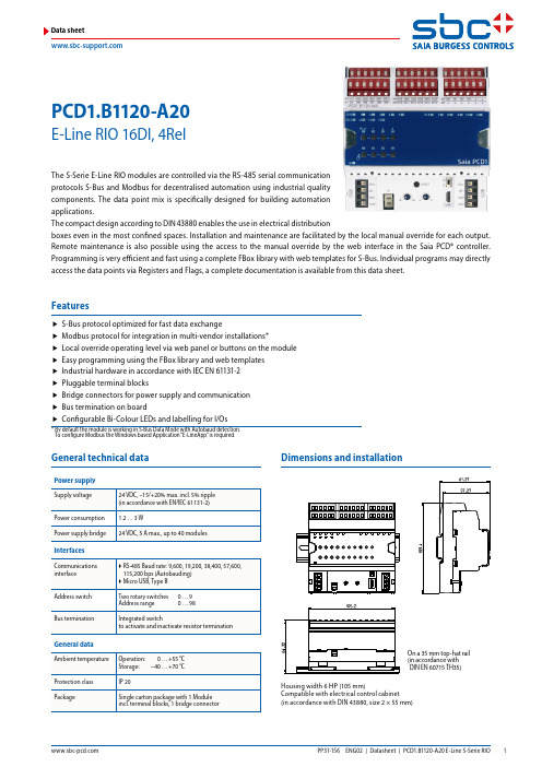
PCD1.B1120-A20E-Line RIO 16DI, 4RelData sheetDimensions and installationf S-Bus protocol optimized for fast data exchangef Modbus protocol for integration in multi-vendor installations*f Local override operating level via web panel or buttons on the module f Easy programming using the FBox library and web templates f Industrial hardware in accordance with IEC EN 61131-2 f Pluggable terminal blocksf Bridge connectors for power supply and communication f Bus termination on boardf Configurable Bi-Colour LEDs and labelling for I/Os* B y default the module is working in S-Bus Data Mode with Autobaud detection. To configure Modbus the Windows based Application “E-LineApp” is required.FeaturesOn a 35 mm top-hat rail ( i n accordance with DIN EN 60715 TH35)General technical dataPower supplyThe S-Serie E-Line RIO modules are controlled via the RS-485 serial communication protocols S-Bus and Modbus for decentralised automation using industrial quality components. The data point mix is specifically designed for building automation applications.The compact design according to DIN 43880 enables the use in electrical distributionboxes even in the most confined spaces. Installation and maintenance are facilitated by the local manual override for each output. Remote maintenance is also possible using the access to the manual override by the web interface in the Saia PCD® controller. Programming is very efficient and fast using a complete FBox library with web templates for S-Bus. Individual programs may directly access the data points via Registers and Flags, a complete documentation is available from this data sheet.Housing width 6 HP (105 mm)Compatible with electrical control cabinet (in accordance with DIN 43880, size 2 × 55mm)/DA+DB-GND+24VOpenClose For easy installation the power supply and communicationbus is available together at one connector. The push-in springterminals enable wiring as well support the connector bridge.Push-in spring terminals enable wiring with rigid or flexible wireswith a diameter up to 1.5 mm². A max. of 1 mm² is permitted withcable end sleeves.Terminal technologyConnection conceptOFF No PowerGreen Communication OKGreen blink Auto bauding in progressOrange No communicationRed ErrorRed/Green alternate B ooter mode(e.g. during Firmware download)Red blink Internal fatal errorStatus LEDThe module provides an active bus termination. It is switchedoff by factory default. To enable the termination, the switchneed to be in the “Close” position.Bus terminationThe USB interface provides access to the communicationprotocol configuration. Firmware updates can also be downloaded via Saia PG5® Firmware Download tool.Service interfaceReset buttonPushed over 20 seconds: The button needs to be pushed forminimum 20 seconds and released during the first minute afterpower up. All user settings are reset to factory default values.Pushed at power up: Power off the device and press thebutton. Power on and release the button before 5 seconds havepassed. The device stays in boot mode for further actions likefirmware download etc.X4 X8PCD1.B5000-A20LI 0RL 0Input/output configurationDigital inputsRelaysAssignment overviewGND +24V/DA+DB–GND +24V/DA+DB–Connection diagramsDigital inputs24 VDCRelay outputRelay changeoverSource operationPower supply and bus terminationOFF No Power Green Communication OK Green blink Auto bauding in progress Orange No communication Red Error Red/Green alternate B ooter mode(e.g. during Firmware download)Red blink Internal fatal errorStatus LEDLED SignalisationThe Output indication LED can be configured in colour and blink code separately for output state Low and High. LED colour f Off f Red f Green*f Orange (red + green)LED blink code f No blink*f Slow blinking (0.5 flashes per second) f Fast blinking (2 flashes per second)*Factory defaultDigital outputThe Manual override LED is Off in automatic mode and orange in case of manual override is active. LED colour f Off (automatic)f Orange manual mode active LED blink codef No blink (local manual override)f Blinking 1 flash per second (remote manual override)Manual modef Data exchange for I/O via optimised S-Busf Configurable save state for bus interruption or timeoutf Direct generation of the symbolsf Reading and writing of the status of the manual override statusf Direct compatibility with web macrosThe modules are addressed and programmed with Saia PG5® Fupla FBoxes. Web templates are available for theoperation and visualisation of the manual override function.Further information, including which FBoxes are supported,Getting Started, etc., can be found on our support page.FuplaCommunication FBoxProgrammingBy using the local override function, commissioning can takeplace independently of the master station.In addition, the manual operation can also be controlledremotely using a touch panel. If the bus line is cut off, themodule keeps the manually set values. Traditional manualoperation in the control cabinet door via potentiometers andswitches can therefore be completely replaced by this solution. E-Line libraryWeb templates are available for the operation and visualisationof the manual override function.Web templatesfrom the E-Line library. Mixed mode operation is not recommended.E-Line RIOs support the device setup by a windows application program connected via USB. The installer is available for down-load from the SBC support page: E-Line RIO IO Modules.The Baudrate can be defined as automatic detection(default) or set to a specific value. The drop down choice willbe available when the check box “Automatic” is unchecked.TN delay and TS delay shall be left at their default values of 2.Create a new device configurationOpen an existing device configurationSave the current settings as device configurationUpload configuration from the deviceDownload settings to the deviceThe serial communication protocol can be defined either asS-Bus or Modbus. By default the modules are delivered fromfactory with S-Bus.S-Bus settingsThe station number can be set by the rotary switches at thedevice in the range of 0 … 98. If the rotary switches are set toposition 99 the station number can be defined by the deviceconfiguration in a range of 0 … 253.Modbus settingsThe Baudrate is set by default to 115 k. It can be defined aschoice of the list.For best interoperability the Parity Mode and number ofStop Bits can also be set.S-Bus communication is based on Saia PCD® S-Bus Data Mode. Only the set-up of a unique S-Bus address within the communi-cation line is required to establish a communication between Saia PCD® controllers and E-Line RIO modules. The address can be set by the rotary switches at the front of the module. The baud rate will be learned from the network by factory default. In addition a Windows based application is available for manual parameter setup. Configuration parameters as well as manual override state and value are saved non-volatile. A delay of about one second between a manual state change and none volatile saving has to be taken into consideration.Device address f 0 … 98 Address is taken from the rotary switchesf 99Address is taken from the device configuration. The address is settable with the E-Line configuration software.Start-up procedure f Reboot: All outputs are cleared (Off state) f < 1 sec.Output in manual operation are set according to the state before power down.f Outputs in automatic modeIs no telegram received after reboot within the “safe state power-on timeout” the module enters into the safe state mode and sets the outputs according to their configured values.On reception of a valid command telegram the outputs are controlled by the communication. When no communication update followed within the “safe state com. timeout” the module enters into safe state and sets the outputs according to their configured values.Usage of the E-Line module specific FBoxesThe usage of the E-Line module specific FBoxes from the E-Line S-Bus Fupla library allows an easy and efficient commissioning of the E-Line RIO.The FBox allow to define and configure all possible functionalities of the E-Line RIO like manual override permission, usage of safe state mode, behaviour and colour of the LED’s and so on.In the background, the FBox does use the fast ‘E-Line S-Bus’ protocol for a high speed communication between the master and the RIO.The following chapter describes the media and parameter mapping to Registers and Flags for individual programming. For efficient PCD programming the E-Line RIO FBox family and templates are suitable for most applications. Only individual pro-gramming (e.g. Instruction List) require standard S-Bus communication.Digital inputsNormal operation: The outputs are set according the flag set by the communication.Manual operation: The output are set according to the manual command, the communication flags are ignored. Safe State: In case of a broken communication, a safe state value can be applied, see table Safe State Configuration. Register format for manual override via S-Bus (Reg. 90 … 93): Bit 0 Current output value Bit 30 1: output is driven in manual override by S-Bus Bit 31 1: output is driven in manual override by local push buttons Register format for local manual override (Reg. 94 … 97): Bit 0 Current output value Bit 311: output is driven in manual override by local push buttonsRelay outputs** W riting to these registers has no effect. Used only if hardware permission is set in the configurationDirect access to the RIO media with standard S-Bus send and receive telegramsThe LEDs can be configured individually depending on the I/O state in colour and blink code.LED ConfigurationRegister format:Bit 0 ... 7 I/O state Low LED colour Bit 8 ... 15 I/O state Low LED blink code Bit 16 ... 23 I/O state High LED colour Bit 24 (31)I/O state High LED blink codeLED colour 0: Off1: Red2: G reen 3: Orange (red + green)LED blink code 0: No blink 1: Slow blinking (0.5 flashes per second) 2: Fast blinking (2 flashes per second)Factory default:Low: off, High: LED colour 2 (green), no blinkDigital inputsConfiguration for safe state and manual overrideManual operation mode:f Disabled (0)f Local operation only (4, Bit 2 set)f Local operation enabled, remote limited (6, Bit 1 and 2 set), defaultf Local and remote operation enabled (12, Bit 2 and 3 set)f Remote operation only, local operation disabled (8, Bit 3 set)The safe state enable flag and the safe state value are combined in the following way: Setting the enable flag to 0 keep the output value unchanged in case of safe state occurrence.Setting the enable flag to 1 writes the safe state value in case of safe state occurrence.Device Information*** The four registers contain the ASCII characters of the product type.E.g. for PCD1.A2000-A20:0605: 50434431H 0606: 2E413230H 0607: 30302D41H 0608: 32300000HModbus fulfils the requirements for standard communication protocols. It is based on Modbus RTU. The Windows based configu-ration software is required to enable and set up the Modbus communication parameters. The device address can be set up with the rotary switches at the front of the module. Configuration parameters as well as manual override state and value are saved non-volatile. A delay of about one second between a manual state change and non-volatile saving has to be taken into consideration. Device addressf0 … 98 Address is taken from the rotary switchesf99 Address is taken from the device configuration. The address is settable with the E-Line configuration soft-ware.Start-up proceduref Reboot: All outputs are cleared (Off state)f<1 sec. Output in manual operation are set according to the state before power down.f Outputs in automatic modeIs no telegram received after reboot within the “safe state power-on timeout” the module enters as will intothe safe state mode and sets the outputs according to their configured values.On reception of a valid command telegram the outputs are controlled by the communication. When no com-munication update followed within the “safe state com. timeout” the module enters into safe state and setsthe outputs according to their configured values.The following chapter describes the media and parameter mapping to Registers and Flags (=Coils).Supported Modbus services:f Function code 1 (read outputs)f Function code 3 (read registers)f Function code 15 (write multiple outputs)f Function code 16 (write multiple registers)The CRC has to be calculated over all telegram bytes starting with address field up to the last data byte. The CRC has to be attached to the data. Please find an example at the appendix of this document. For more details, please refer the publicly available Modbus documentation .Normal operation: The outputs are set according the flag set by the communication.Manual operation: The output are set according to the manual command, the communication flags are ignored.Safe State: In case of a broken communication, a safe state value can be applied, see table Safe State Configuration.Register format for manual override via Modbus (Reg. 180 … 187):Bit 0 Current output value Enable Reg. Bit 14 1: output is driven in manual override by Modbus Enable Reg. Bit 15 1: output is driven in manual override by local push buttons Register format for local manual override (Reg. 188 … 195):Value Reg. Bit 0 Current output value Enable Reg. Bit 15 1: output is driven in manual override by local push buttonsRelay outputs Digital outputs** Writing to these registers has no effect. Used only if hardware permission is set in the configurationDigital inputsLED ConfigurationOutput L, Bit 0 … 7 I/O state Low LED colourOutput L, Bit 8 … 15 I/O state Low LED blink codeOutput H, Bit 0 … 7 I/O state High LED colourOutput H, Bit 8 … 15 I/O state High LED blink codeLED colour 0: Off1: Red2: Green3: Orange (red + green)LED blink code 0: No blink1: Slow blinking (0.5 flashes per second)2: Fast blinking (2 flashes per second)Factory default: L ow: off,High: LED colour 2 (green), no blinkThe LEDs can be configured individually depending on the I/O state in colour and blink code.Configuration for safe state and manual overrideManual operation mode:f Disabled (0)f Local operation only (4, Bit 2 set)f Local operation enabled, remote limited (6, Bit 1 and 2 set), defaultf Local and remote operation enabled (12, Bit 2 and 3 set)f Remote operation only, local operation disabled (8, Bit 3 set)The safe state enable flag and the safe state value are combined in the following way: Setting the enable flag to 0 keep the output value unchanged in case of safe state occurrence.Setting the enable flag to 1 writes the safe state value in case of safe state occurrence.Device Information1210…1217: 5043H | 4431H | 2E41H | 3230H | 3030H | 2D41H | 3230H | 0000HCRC Generation ExampleThe function takes two arguments: unsigned char *puchMsg; A pointer to the message buffer containing binary data to be used for unsigned short High-Order Byte TableLow-Order Byte Table(Source: /docs/PI_MBUS_300.pdf , the following content of this page is copied from the referenced document. In case of any questions, please check out the original source)generating the CRC unsigned short usDataLen; The quantity of bytes in the message buffer. The function returns the CRC as a type unsigned short.CRC Generation FunctionCRC16(puchMsg, usDataLen) ; unsigned char *puchMsg ; /* message to calculate CRC upon */ unsigned short usDataLen ; /* quantity of bytes in message */ { unsigned char uchCRCHi = 0xFF ; /* high byte of CRC initialized */ unsigned char uchCRCLo = 0xFF ; /* low byte of CRC initialized */ unsigned uIndex ; /* will index into CRC lookup table */ while (usDataLen--) /* pass through message buffer */ { uIndex = uchCRCHi ^ *puchMsgg++; /* calculate the CRC */ uchCRCHi = uchCRCLo ^ auchCRCHi[uIndex]; uchCRCLo = auchCRCLo[uIndex]; } return (uchCRCHi << 8 | uchCRCLo); }/* Table of CRC values for high-order byte */ static unsigned char auchCRCHi[] = {0x00, 0xC1, 0x81, 0x40, 0x01, 0xC0, 0x80, 0x41, 0x01, 0xC0, 0x80, 0x41, 0x00, 0xC1, 0x81, 0x40, 0x01, 0xC0, 0x80, 0x41, 0x00, 0xC1, 0x81, 0x40, 0x00, 0xC1, 0x81, 0x40, 0x01, 0xC0, 0x80, 0x41, 0x01, 0xC0, 0x80, 0x41, 0x00, 0xC1, 0x81, 0x40, 0x00, 0xC1, 0x81, 0x40, 0x01, 0xC0, 0x80, 0x41, 0x00, 0xC1, 0x81, 0x40, 0x01, 0xC0, 0x80, 0x41, 0x01, 0xC0, 0x80, 0x41, 0x00, 0xC1, 0x81, 0x40, 0x01, 0xC0, 0x80, 0x41, 0x00, 0xC1, 0x81, 0x40, 0x00, 0xC1, 0x81, 0x40, 0x01, 0xC0, 0x80, 0x41, 0x00, 0xC1, 0x81, 0x40, 0x01, 0xC0, 0x80, 0x41, 0x01, 0xC0, 0x80, 0x41, 0x00, 0xC1, 0x81, 0x40, 0x00, 0xC1, 0x81, 0x40, 0x01, 0xC0, 0x80, 0x41, 0x01, 0xC0, 0x80, 0x41, 0x00, 0xC1, 0x81, 0x40, 0x01, 0xC0, 0x80, 0x41, 0x00, 0xC1, 0x81, 0x40, 0x00, 0xC1, 0x81, 0x40, 0x01, 0xC0, 0x80, 0x41, 0x01, 0xC0, 0x80, 0x41, 0x00, 0xC1, 0x81, 0x40, 0x00, 0xC1, 0x81, 0x40, 0x01, 0xC0, 0x80, 0x41, 0x00, 0xC1, 0x81, 0x40, 0x01, 0xC0, 0x80, 0x41, 0x01, 0xC0, 0x80, 0x41, 0x00, 0xC1, 0x81, 0x40, 0x00, 0xC1, 0x81, 0x40, 0x01, 0xC0, 0x80, 0x41, 0x01, 0xC0, 0x80, 0x41, 0x00, 0xC1, 0x81, 0x40, 0x01, 0xC0, 0x80, 0x41, 0x00, 0xC1, 0x81, 0x40, 0x00, 0xC1, 0x81, 0x40, 0x01, 0xC0, 0x80, 0x41, 0x00, 0xC1, 0x81, 0x40, 0x01, 0xC0, 0x80, 0x41, 0x01, 0xC0, 0x80, 0x41, 0x00, 0xC1, 0x81, 0x40, 0x01, 0xC0, 0x80, 0x41, 0x00, 0xC1, 0x81, 0x40, 0x00, 0xC1, 0x81, 0x40, 0x01, 0xC0, 0x80, 0x41, 0x01, 0xC0, 0x80, 0x41, 0x00, 0xC1, 0x81, 0x40, 0x00, 0xC1, 0x81, 0x40, 0x01, 0xC0, 0x80, 0x41, 0x00, 0xC1, 0x81, 0x40, 0x01, 0xC0, 0x80, 0x41, 0x01, 0xC0, 0x80, 0x41, 0x00, 0xC1, 0x81, 0x40 }; /* Table of CRC values for low-order byte */ static char auchCRCLo[] = {0x00, 0xC0, 0xC1, 0x01, 0xC3, 0x03, 0x02, 0xC2, 0xC6, 0x06, 0x07, 0xC7, 0x05, 0xC5, 0xC4, 0x04, 0xCC , 0x0C , 0x0D , 0xCD , 0x0F , 0xCF , 0xCE , 0x0E , 0x0A , 0xCA , 0xCB , 0x0B , 0xC9, 0x09, 0x08, 0xC8, 0xD8, 0x18, 0x19, 0xD9, 0x1B , 0xDB , 0xDA , 0x1A , 0x1E , 0xDE , 0xDF , 0x1F , 0xDD , 0x1D , 0x1C , 0xDC , 0x14, 0xD4, 0xD5, 0x15, 0xD7, 0x17, 0x16, 0xD6, 0xD2, 0x12, 0x13, 0xD3, 0x11, 0xD1, 0xD0, 0x10, 0xF0, 0x30, 0x31, 0xF1, 0x33, 0xF3, 0xF2, 0x32, 0x36, 0xF6, 0xF7, 0x37, 0xF5, 0x35, 0x34, 0xF4, 0x3C , 0xFC , 0xFD , 0x3D , 0xFF , 0x3F , 0x3E , 0xFE , 0xFA , 0x3A , 0x3B , 0xFB , 0x39, 0xF9, 0xF8, 0x38, 0x28, 0xE8, 0xE9, 0x29, 0xEB , 0x2B , 0x2A , 0xEA , 0xEE , 0x2E , 0x2F , 0xEF , 0x2D , 0xED , 0xEC , 0x2C , 0xE4, 0x24, 0x25, 0xE5, 0x27, 0xE7, 0xE6, 0x26, 0x22, 0xE2, 0xE3, 0x23, 0xE1, 0x21, 0x20, 0xE0, 0xA0, 0x60, 0x61, 0xA1, 0x63, 0xA3, 0xA2, 0x62, 0x66, 0xA6, 0xA7, 0x67, 0xA5, 0x65, 0x64, 0xA4, 0x6C , 0xAC , 0xAD , 0x6D , 0xAF , 0x6F , 0x6E , 0xAE , 0xAA , 0x6A , 0x6B , 0xAB , 0x69, 0xA9, 0xA8, 0x68, 0x78, 0xB8, 0xB9, 0x79, 0xBB , 0x7B , 0x7A , 0xBA , 0xBE , 0x7E , 0x7F , 0xBF , 0x7D , 0xBD , 0xBC , 0x7C , 0xB4, 0x74, 0x75, 0xB5, 0x77, 0xB7, 0xB6, 0x76, 0x72, 0xB2, 0xB3, 0x73, 0xB1, 0x71, 0x70, 0xB0, 0x50, 0x90, 0x91, 0x51, 0x93, 0x53, 0x52, 0x92, 0x96, 0x56, 0x57, 0x97, 0x55, 0x95, 0x94, 0x54, 0x9C , 0x5C , 0x5D , 0x9D , 0x5F , 0x9F , 0x9E , 0x5E , 0x5A , 0x9A , 0x9B , 0x5B , 0x99, 0x59, 0x58, 0x98, 0x88, 0x48, 0x49, 0x89, 0x4B , 0x8B , 0x8A , 0x4A , 0x4E , 0x8E , 0x8F , 0x4F , 0x8D , 0x4D , 0x4C , 0x8C , 0x44, 0x84, 0x85, 0x45, 0x87, 0x47, 0x46, 0x86, 0x82, 0x42, 0x43, 0x83, 0x41, 0x81, 0x80, 0x40 };Wiring example with fuses Relay changeoverPCD1.K0206-005PCD1.K0206-025PCD1.B1120-A20Saia-Burgess Controls AGBahnhofstrasse 18 | 3280 Murten, Switzerland T +41 26 580 30 00 | F +41 26 580 34 ********************|Order detailsTerminal set 32304321-003-S。
最新常用Proteus元件库

常用P r o t e u s元件库AND 与门ANTENNA 天线BATTERY 直流电源BELL 铃,钟BVC 同轴电缆接插件BRIDEG 1 整流桥(二极管) BRIDEG 2 整流桥(集成块) BUFFER 缓冲器BUZZER 蜂鸣器CAP 电容CAPACITOR 电容CAPACITOR POL 有极性电容CAPVAR 可调电容CIRCUIT BREAKER 熔断丝COAX 同轴电缆CON 插口CRYSTAL 晶体整荡器DB 并行插口DIODE 二极管DIODE SCHOTTKY 稳压二极管DIODE VARACTOR 变容二极管DPY_3-SEG 3段LEDDPY_7-SEG 7段LEDDPY_7-SEG_DP 7段LED(带小数点) ELECTRO 电解电容FUSE 熔断器INDUCTOR 电感INDUCTOR IRON 带铁芯电感INDUCTOR3 可调电感JFET N N沟道场效应管JFET P P沟道场效应管LAMP 灯泡LAMP NEDN 起辉器LED 发光二极管METER 仪表MICROPHONE 麦克风MOSFET MOS管MOTOR AC 交流电机MOTOR SERVO 伺服电机NAND 与非门仅供学习与交流,如有侵权请联系网站删除谢谢7NOR 或非门NOT 非门NPN NPN三极管NPN-PHOTO 感光三极管OPAMP 运放OR 或门PHOTO 感光二极管PNP 三极管NPN DAR NPN三极管PNP DAR PNP三极管POT 滑线变阻器PELAY-DPDT 双刀双掷继电器RES1.2 电阻RES3.4 可变电阻RESISTOR BRIDGE ? 桥式电阻RESPACK ? 电阻SCR 晶闸管PLUG ? 插头PLUG AC FEMALE 三相交流插头SOCKET ? 插座SOURCE CURRENT 电流源SOURCE VOLTAGE 电压源SPEAKER 扬声器SW ? 开关SW-DPDY ? 双刀双掷开关SW-SPST ? 单刀单掷开关SW-PB 按钮THERMISTOR 电热调节器TRANS1 变压器TRANS2 可调变压器TRIAC ? 三端双向可控硅TRIODE ? 三极真空管VARISTOR 变阻器ZENER ? 齐纳二极管DPY_7-SEG_DP 数码管SW-PB 开关元件名称中文名说明7407 驱动门1N914 二极管74Ls00 与非门74LS04 非门74LS08 与门74LS390 TTL 双十进制计数器仅供学习与交流,如有侵权请联系网站删除谢谢77SEG 4针BCD-LED 输出从0-9 对应于4根线的BCD码7SEG 3-8译码器电路BCD-7SEG转换电路AlterNATOR 交流发电机AMMETER-MILLI mA安培计AND 与门BATTERY 电池/电池组BUS 总线CAP 电容CAPACITOR 电容器CLOCK 时钟信号源CRYSTAL 晶振Compim 串口D-FLIPFLOP D触发器FUSE 保险丝GROUND 地LAMP 灯LED-RED 红色发光二极管LM016L 2行16列液晶可显示2行16列英文字符,有8位数据总线D0-D7,RS,R/W,EN三个控制端口(共14线),工作电压为5V。
3296电位器

200圈 △R≤±10%R,CRV≤3%R或5Ω
按IEC68-2-3,Ca,96h △R≤±10%R,△R1≥100MΩ
28±2圈 ≤35mN·m 阻值允许偏差(±10%不标注) 阻值代码,产品型号
标准包装
50只/管
640Vac 100mA >总机械行程的70%
环境特性
额定功率 温度范围 温度系数
碰撞 温度变化 循环5次
振动
气候顺序
0.5W@+70℃ ,OW@+100℃ -55℃—+100℃
±250ppm/℃,±100ppm/℃ 390m/s2,4000次,△R≤±5%R
-55℃,30min,+100℃,30min △R≤±5%R,△(Uab/Uac)≤±5%R
10—500Hz,0.75mm,6h 电气间断≤100