FIFO的verilog代码
【CPLD Verilog】CPLD实现同步FIFO
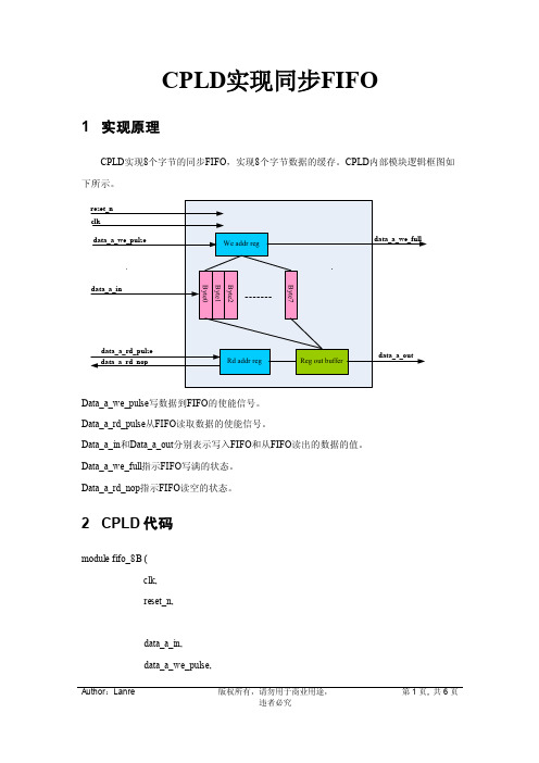
CPLD实现同步FIFO1 实现原理CPLD实现8个字节的同步FIFO,实现8个字节数据的缓存。
CPLD内部模块逻辑框图如下所示。
Data_a_we_pulse写数据到FIFO的使能信号。
Data_a_rd_pulse从FIFO读取数据的使能信号。
Data_a_in和Data_a_out分别表示写入FIFO和从FIFO读出的数据的值。
Data_a_we_full指示FIFO写满的状态。
Data_a_rd_nop指示FIFO读空的状态。
2 CPLD代码module fifo_8B (clk,reset_n,data_a_in,data_a_we_pulse,data_a_we_full,data_a_out,data_a_rd_pulse,data_a_rd_nop);input clk;input reset_n;input [7:0] data_a_in;input data_a_we_pulse;output data_a_we_full;output [7:0] data_a_out;input data_a_rd_pulse;output data_a_rd_nop;//////////////////////////FIFO 写入数据逻辑////////////////////////////reg [7:0] fifo_mem [7:0]; //FIFO空间,8个8bit的空间reg [2:0] fifo_we_addr; //FIFO写地址寄存器reg fifo_we_addr_reverse_pulse; //FIFO写地址翻转状态寄存器,用于指示写//地址是否从最大地址翻转回到最小地址always@(posedge clk or negedge reset_n)beginif(reset_n == 1'b0)beginfifo_we_addr <= 3'h0;fifo_we_addr_reverse_pulse <= 1'b0;endelse if((data_a_we_pulse == 1'b1)&&(fifo_we_addr != 3'h7)&&(data_a_we_full == 1'b0)) beginfifo_mem[fifo_we_addr] <= data_a_in; //对应写地址,写入相应的值fifo_we_addr <= fifo_we_addr+3'h1;endelse if((data_a_we_pulse == 1'b1)&&(fifo_we_addr == 3'h7)&&(data_a_we_full == 1'b0)) beginfifo_mem[fifo_we_addr] <= data_a_in;fifo_we_addr <= fifo_we_addr+3'h1;fifo_we_addr_reverse_pulse <= ~fifo_we_addr_reverse_pulse;endelse;end//////////////////////////FIFO 读出数据逻辑////////////////////////////reg [2:0] fifo_rd_addr; //FIFO读地址寄存器reg fifo_rd_addr_reverse_pulse; //FIFO读地址翻转状态寄存器,用于指示读//地址是否从最大地址翻转回到最小地址reg [7:0] data_a_out;always@(posedge clk or negedge reset_n)beginif(reset_n == 1'b0)beginfifo_rd_addr <= 3'h0;fifo_rd_addr_reverse_pulse <= 1'b0;endelse if((data_a_rd_pulse == 1'b1)&&(fifo_rd_addr != 3'h7)&&(data_a_rd_nop == 1'b0)) begindata_a_out <= fifo_mem[fifo_rd_addr]; //对应读地址,读出相应的值fifo_rd_addr <= fifo_rd_addr+3'h1;endelse if((data_a_rd_pulse == 1'b1)&&(fifo_rd_addr == 3'h7)&&(data_a_rd_nop == 1'b0)) begindata_a_out <= fifo_mem[fifo_rd_addr];fifo_rd_addr <= fifo_rd_addr+3'h1;fifo_rd_addr_reverse_pulse <= ~fifo_rd_addr_reverse_pulse;endelse;end//////////////////////////FIFO 满空逻辑////////////////////////////wire fifo_addr_reverse_flag;assign fifo_addr_reverse_flag = (fifo_we_addr_reverse_pulse^fifo_rd_addr_reverse_pulse == 1'b1) ? 1'b1 : 1'b0;reg data_a_we_full;reg data_a_rd_nop;always@(posedge clk or negedge reset_n)beginif(reset_n == 1'b0)begindata_a_we_full <= 1'b0;data_a_rd_nop <= 1'b1;endelse if((fifo_rd_addr == fifo_we_addr)&&(fifo_addr_reverse_flag ==1'b1))begindata_a_we_full <= 1'b1;data_a_rd_nop <= 1'b0;endelse if((fifo_rd_addr == fifo_we_addr)&&(fifo_addr_reverse_flag ==1'b0))begindata_a_we_full <= 1'b0;data_a_rd_nop <= 1'b1;endelsebegindata_a_we_full <= 1'b0;data_a_rd_nop <= 1'b0;endendendmodule3 仿真结果3.1 正常写入读取FIFO仿真如下红色圆框,红色圆框表示向FIFO写入3个字节数据,红色方框表示从FIFO读取出2个字节数据。
verilog同步和异步FIFO,可直接仿真和综合解读
EDA/SOPC课程设计报告题目:同异步FIFO模块的设计与验证姓名:xxx学号:120260320同组人:xxx指导教师:xxx成绩:目录目录 (II)第1章课程设计的要求 (1)1.1 课程设计的目的 (1)1.2 课程设计的条件 (1)1.3 课程设计的要求 (1)第2章课程设计的内容 (2)2.1 设计思路 (2)2.2 软件流程图 (2)2.3 HDL代码阐述 (2)2.4 ModelSim验证 (2)第3章课程设计的心得 (3)第1章课程设计的要求1.1 课程设计的目的●掌握FIFO设计的基本原理与方法●培养Verilog语言模块化设计的思想意识●完成一个FIFO的设计与验证●掌握较大工程的基本开发技能●培养综合运用Modelsim工具进行硬件开发的能力●培养数字系统设计的基本能力●加强对课堂Verilog语言学习的理解与升华1.2 课程设计的条件●设计条件ISE、Modelsim等开发软件的使用1.3 课程设计的要求●设计要求1 设计同步FIFO并验证(包括仿真验证、FPGA验证)●设计要求2 设计异步FIFO并验证(包括仿真验证、FPGA验证)●设计要求3 采用Design Compiler完成其逻辑综合,评估其面积和时序●设计要求4 完成综合后的SDF反标仿真第2章课程设计的内容2.1 设计思路FIFO(First Input First Output),即先进先出队列。
在计算机中,先入先出队列是一种传统的按序执行方法,先进入的指令先完成并引退,跟着才执行第二条指令(指令就是计算机在响应用户操作的程序代码,对用户而言是透明的)。
如下图所示,当CPU在某一时段来不及响应所有的指令时,指令就会被安排在FIFO队列中,比如0号指令先进入队列,接着是1号指令、2号指令……当CPU完成当前指令以后就会从队列中取出0号指令先行执行,此时1号指令就会接替0号指令的位置,同样,2号指令、3号指令……都会向前挪一个位置,这样解释大家清楚了吧?在设计之初,我们只对FIFO有一个模糊的了解,只知道它是一个先入先出的队列,但是对于它是如何组成和如何工作并不了解,于是我们设计的首要任务就是查阅资料,逐步完善我们对于同步FIFO和异步FIFO的了解。
verilogfifo读写详细讲解
verilogfifo读写详细讲解FIFO是一种先进先出的数据结构,其全称为First-In-First-Out。
在Verilog中,可以使用以下代码实现FIFO的读写操作。
首先,我们需要定义FIFO的模块。
如下所示:```verilogmodule fifo #(parameter DATA_WIDTH = 8) (input clk, // 时钟信号input reset, // 复位信号input read, // 读使能信号input write, // 写使能信号input [DATA_WIDTH-1:0] data_in, // 输入数据output reg [DATA_WIDTH-1:0] data_out, // 输出数据output reg empty, // FIFO为空信号output reg full // FIFO为满信号);```在FIFO的模块中,我们定义了以下信号:clk表示时钟信号,reset表示复位信号,read表示读使能信号,write表示写使能信号,data_in表示输入数据,data_out表示输出数据,empty表示FIFO为空信号,full表示FIFO为满信号。
在模块的内部,我们可以使用一个或多个寄存器来实现FIFO的功能。
在这里,我们使用两个寄存器data_reg和next_data_reg来存储数据,使用两个计数器empty_count和full_count来记录FIFO的空和满状态。
```verilogreg [DATA_WIDTH-1:0] data_reg; // 数据寄存器reg [DATA_WIDTH-1:0] next_data_reg; // 下一个数据寄存器reg [DATA_WIDTH-1:0] data_out_reg; // 输出数据寄存器reg empty_count; // 空计数器reg full_count; // 满计数器```接下来,我们定义FIFO的行为。
FIFO的verilog语言代码(含测试代码)
FIFO的verilog语言代码(含测试代码)FIFO存储器的设计(后面是测试程序的部分)module fifo (clk, rstp, din, writep, readp, dout, emptyp, fullp);input clk;input rstp; //复位信号input [15:0] din;input readp; //读信号input writep; //写信号output [15:0] dout;output emptyp; //空标志output fullp; //满标志parameter DEPTH = 2,MAX_COUNT = 2‘b11; //定义地址最大值reg emptyp;reg fullp;reg [15:0] dout;reg [(DEPTH-1):0] tail; //定义读指针reg [(DEPTH-1):0] head; //定义写指针// 定义计数器reg [(DEPTH-1):0] count;reg [15:0] fifomem[0:MAX_COUNT]; //定义fifomem存储器有4个16位的存储器// dout被赋给tail指向的值always @(posedge clk) beginif (rstp == 1) begindout <= 16‘h0000; //复位信号有效置0endelse begindout <= fifomem[tail]; //将fifomem中第tail个单元赋给dout endendalways @(posedge clk) beginif (rstp == 1'b0 && writep == 1'b1 && fullp == 1'b0) begin fifomem[head] <= din; //写入endendalways @(posedge clk) beginif (rstp == 1'b1) beginhead <= 2‘b00; //复位endelse beginif (writep == 1'b1 && fullp == 1'b0) beginhead <= head + 1;endendendalways @(posedge clk) beginif (rstp == 1'b1) begintail <= 2‘b00; //复位endelse beginif (readp == 1'b1 && emptyp == 1'b0) begintail <= tail + 1;endendendalways @(posedge clk) beginif (rstp == 1'b1) begincount <= 2'b00;endelse begincase ({readp, writep})2'b00: count <= count;2'b01:if (count != MAX_COUNT)count <= count + 1; //为写状态时计数器进行加法计数2'b10:if (count != 2'b00)count <= count - 1; //为读状态计数器进行减法计数2'b11:count <= count;endcaseendendalways @(count) beginif (count == 2'b00)emptyp <= 1‘b1; //count为0时emptyp赋为1 elseemptyp <= 1'b0;endalways @(count) beginif (count == MAX_COUNT)fullp <= 1‘b1; //计数到最大时fullp赋为1elsefullp <= 1'b0;endendmodule/************************************************************** *****************************/测试程序:module test_fifo;reg clk;reg rstp;reg [15:0] din;reg readp;reg writep;wire [15:0] dout;wire emptyp;wire fullp;reg [15:0] value;fifo U1 (.clk(clk),.rstp(rstp),.din(din),.readp(readp),.writep(writep),.dout(d out),.emptyp(emptyp),.fullp(fullp));task read_word;begin@(negedge clk);readp = 1;@(posedge clk) #5; readp = 0;endendtasktask write_word; input [15:0] value; begin@(negedge clk);din = value;writep = 1;@(posedge clk);#5;din = 16'hzzzz; writep = 0;endendtaskinitial beginclk = 0;forever begin#10 clk = 1;#10 clk = 0;endendinitial begin//test1;test2; //调用测试模块2task test1;begindin = 16'hzzzz;writep = 0;readp = 0;rstp = 1;#50 rstp = 0;#50;write_word (16'h1111);write_word (16'h2222);write_word (16‘h3333); //写入3个数据read_word;read_word; //读两个write_word (16‘h4444); //在写一个数据repeat (6) beginread_word;endwrite_word (16'h0001);write_word (16'h0002);write_word (16'h0003);write_word (16'h0004);write_word (16'h0005);write_word (16'h0006);write_word (16'h0007);write_word (16'h0008);repeat (6) beginread_word;endendtasktask test2;reg [15:0] writer_counter;beginwriter_counter = 16'h0001;din = 16'hzzzz;writep = 0;readp = 0;rstp = 1;#50 rstp = 0;#50;fork//写数据beginrepeat (500) begin@(negedge clk);if (fullp == 1'b0) beginwrite_word (writer_counter);#5;writer_counter = writer_counter + 1; end#50;endend//读数据forever begin@(negedge clk);if (emptyp == 1'b0) begin read_word;end#50;endendjoinendendtaskendmodule。
基于verilog HDL 硬件描语言的FIFO设计
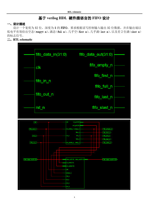
基于verilog HDL 硬件描语言的FIFO设计一、设计描述设计一个宽度为32位,深度为8的FIFO,要求根据读写控制输入输出32位数据,并在输出端以低电平有效给出空态(empyt_n),满态(full_n),几乎空(first_n),几乎满(last_n),以及差2位满(slast_n)的标志信号。
二、RTL schematic三、RTL源代码// -------------------------------------------------------------------------------------------------// File name: fifo_ctrl.v--------xjy// ------------------------------------------------------------------------------------------------//`timescale 1ns/1psmodule fifo_ctrl(clk,rst_n,wrt_strobe_n,rd_strobe_n,// clr_n,rd_ptr,wrt_ptr,full_n,empty_n,last_n,slast_n,first_n);input clk; // FIFO clock domaininput rst_n; // FIFO reset, active lowinput wrt_strobe_n; // fifo write strobe, active lowinput rd_strobe_n; // fifo read strobe, active low//input clr_n; // clear signal, active lowoutput [2:0] rd_ptr; // read pointer to regfileoutput [2:0] wrt_ptr; // write pointer to regfileoutput full_n; // fifo full indicator, active lowoutput empty_n; // fifo empty indicator, active low output last_n; // indicate one space in fifo, active low output slast_n; // indicate two space in fifo, active low output first_n; // indicate only one data in fifo, active low reg [2:0] rd_ptr;reg [2:0] wrt_ptr;wire full_n, empty_n, last_n, slast_n, first_n;reg [3:0] reg_count;///////////////////write pointer////////////////////////always @(posedge clk or negedge rst_n)beginif(!rst_n) wrt_ptr <= 3'b0;else if(wrt_ptr == 3'b111) wrt_ptr <=0;else if((!wrt_strobe_n)&&(full_n)&&(rd_strobe_n))beginwrt_ptr<=(wrt_ptr+1);// wr_mark<=1;endelse beginwrt_ptr<=wrt_ptr;//wr_mark<=0;endend///////////////////read pointer/////////////////////always @(posedge clk or negedge rst_n)beginif(!rst_n) rd_ptr <= 3'b0;else if(rd_ptr == 3'b111) rd_ptr <=0;else if((!rd_strobe_n)&&(empty_n)&&(wrt_strobe_n))beginrd_ptr<= (rd_ptr+1);//rd_mark<=1;endelse beginrd_ptr<=rd_ptr;//rd_mark<=0;endend//////////register counter:from 0(empty) to 8(full)////////always @(posedge clk or negedge rst_n)beginif(!rst_n) reg_count<=0;elsecasez({wrt_strobe_n,rd_strobe_n})2'b01: reg_count <= (full_n) ? (reg_count+1) : reg_count;//write---count+12'b10: reg_count <= (empty_n) ? (reg_count-1) : reg_count;//read---count-1default: reg_count <= reg_count;endcaseend//main blocks--------------------------------------------------assign empty_n=(reg_count==4'b0000)? 0:1;assign full_n=(reg_count==4'b1000)? 0:1;assign last_n=(reg_count==4'b0111)? 0:1;assign slast_n=(reg_count==4'b0110)? 0:1;assign first_n=(reg_count==4'b0001)? 0:1;endmodule// -------------------------------------------------------------------------------------------------// File name : fifo_regfile.v-------xjy// ------------------------------------------------------------------------------------------------//`timescale 1ns/1psmodule fifo_regfile(clk,rst_n,wrt_n,rd_n,rd_addr,wrt_addr,data_in,data_out,full_n,empty_n);input clk; // clk signal.input rst_n; // Low Asserted Reset signal.input rd_n;input wrt_n; // write strobe to fifoinput [2:0] rd_addr; // address for read datainput [2:0] wrt_addr; // address for write datainput [31:0] data_in; // Data into FIFO.input full_n,empty_n; //control read and write/////////////////////// output [31:0] data_out; // FIFO data out.reg [31:0] int_reg_b[7:0];reg [31:0] int_data_out;wire [31:0] data_out = int_data_out[31:0];always @(posedge clk or negedge rst_n)beginif(!rst_n) beginint_reg_b[0] <= 32'h0000;int_reg_b[1] <= 32'h0000;int_reg_b[2] <= 32'h0000;int_reg_b[3] <= 32'h0000;int_reg_b[4] <= 32'h0000;int_reg_b[5] <= 32'h0000;int_reg_b[6] <= 32'h0000;int_reg_b[7] <= 32'h0000; endelse if(!wrt_n)begincasez(wrt_addr[2:0])3'b000: int_reg_b[0] <= (full_n) ? data_in : int_reg_b[0];3'b001: int_reg_b[1] <= (full_n) ? data_in : int_reg_b[1];3'b010: int_reg_b[2] <= (full_n) ? data_in : int_reg_b[2];3'b011: int_reg_b[3] <= (full_n) ? data_in : int_reg_b[3];3'b100: int_reg_b[4] <= (full_n) ? data_in : int_reg_b[4];3'b101: int_reg_b[5] <= (full_n) ? data_in : int_reg_b[5];3'b110: int_reg_b[6] <= (full_n) ? data_in : int_reg_b[6];3'b111: int_reg_b[7] <= (full_n) ? data_in : int_reg_b[7];default: begin //if wrt_addr is x or z.register restainint_reg_b[0] <= int_reg_b[0];int_reg_b[1] <= int_reg_b[1];int_reg_b[2] <= int_reg_b[2];int_reg_b[3] <= int_reg_b[3];int_reg_b[4] <= int_reg_b[4];int_reg_b[5] <= int_reg_b[5];int_reg_b[6] <= int_reg_b[6];int_reg_b[7] <= int_reg_b[7];endendcaseendendalways @(posedge clk or negedge rst_n)beginif(!rst_n)int_data_out<=32'h0000;else if(!rd_n)begincasez(rd_addr[2:0])3'b000: int_data_out <= (empty_n) ? int_reg_b[0] : int_data_out;3'b001: int_data_out <= (empty_n) ? int_reg_b[1] : int_data_out;3'b010: int_data_out <= (empty_n) ? int_reg_b[2] : int_data_out;3'b011: int_data_out <= (empty_n) ? int_reg_b[3] : int_data_out;3'b100: int_data_out <= (empty_n) ? int_reg_b[4] : int_data_out;3'b101: int_data_out <= (empty_n) ? int_reg_b[5] : int_data_out;3'b110: int_data_out <= (empty_n) ? int_reg_b[6] : int_data_out;3'b111: int_data_out <= (empty_n) ? int_reg_b[7] : int_data_out;default: int_data_out <= int_data_out;endcaseendendendmodule// -------------------------------------------------------------------------------------------------------------- // File name: top_fifo.v----------xjy// ---------------------------------------------------------------------------------------------------------------- //`include "fifo_ctrl.v"//`include "fifo_regfile.v"`timescale 1ns/1psmodule top_fifo(clk,rst_n,fifo_data_in,fifo_in_n,fifo_out_n,fifo_data_out,fifo_full_n,fifo_last_n,fifo_slast_n,fifo_first_n,fifo_empty_n);input clk; // clk signal.input rst_n; // Low Asserted Reset signal.input [31:0] fifo_data_in; // Data into FIFO.input fifo_in_n; // Write into FIFO Signal.//input fifo_clr_n; // Clear signal to FIFO.input fifo_out_n; // Read from FIFO signal.output [31:0] fifo_data_out; // FIFO data out.output fifo_full_n; // FIFO full indicating signal.output fifo_empty_n; // FIFO empty indicating signal.output fifo_last_n; // FIFO Last but one signal.output fifo_slast_n; // FIFO SLast but one signal.output fifo_first_n; // Signal indicating only one// word in FIFO.wire [2:0] rd_ptr;wire [2:0] wrt_ptr;wire full_n,empty_n;assign fifo_full_n = full_n;assign fifo_empty_n = empty_n;fifo_regfile u_fifo_regfile(.clk (clk ),.rst_n (rst_n ),.wrt_n (fifo_in_n ),.rd_n (fifo_out_n ),.rd_addr (rd_ptr[2:0] ),.wrt_addr (wrt_ptr[2:0] ),.data_in (fifo_data_in[31:0] ),.data_out (fifo_data_out[31:0] ),.full_n (full_n),.empty_n (empty_n));fifo_ctrl u_fifo_ctrl(.clk (clk ),.rst_n (rst_n ),.wrt_strobe_n (fifo_in_n ),.rd_strobe_n (fifo_out_n ),.rd_ptr (rd_ptr[2:0] ),.wrt_ptr (wrt_ptr[2:0] ),.full_n (full_n ),.empty_n (empty_n ),.last_n (fifo_last_n ),.slast_n (fifo_slast_n ),.first_n (fifo_first_n ));Endmodule附:部分测试文件initialbeginclk=1; rst_n=0; fifo_in_n=1; fifo_out_n=1;#10 rst_n=1; //reset////////formal test////////////#20 fifo_in_n=0; //write enable:in 8 datas#80 fifo_in_n=1; fifo_out_n=0;// read:2 datas#20 fifo_out_n=1; fifo_in_n=0;//write 2#20 fifo_in_n=1; fifo_out_n=0;//read 8 (all)#80 fifo_out_n=1;//---empty///////full---write,empty----read,test#50 fifo_in_n=0; fifo_out_n=1;// write:10 datas only 8 effective #100 fifo_in_n=1; fifo_out_n=0;// read:6 datas#60 fifo_in_n=0; fifo_out_n=1;// write:2 datas#20 fifo_in_n=1; fifo_out_n=0;// read:10 datas only 8 effective #100 fifo_in_n=1; fifo_out_n=1;//#10 $stop;四、综合报告//////////////////////////////////////////SYNTHESIZE REPORT///////////////////////////////////////////////////////////////////// Release 10.1 - xst K.31 (nt)Copyright (c) 1995-2008 Xilinx, Inc. All rights reserved.--> Parameter TMPDIR set to D:/Post-Graduate/CourseWare_10/verilog/FIFO_xjy/xst/projnav.tmpTotal REAL time to Xst completion: 0.00 secsTotal CPU time to Xst completion: 0.16 secs--> Parameter xsthdpdir set to D:/Post-Graduate/CourseWare_10/verilog/FIFO_xjy/xstTotal REAL time to Xst completion: 0.00 secsTotal CPU time to Xst completion: 0.16 secs--> Reading design: top_fifo.prjTABLE OF CONTENTS1) Synthesis Options Summary2) HDL Compilation3) Design Hierarchy Analysis4) HDL Analysis5) HDL Synthesis5.1) HDL Synthesis Report6) Advanced HDL Synthesis6.1) Advanced HDL Synthesis Report7) Low Level Synthesis8) Partition Report9) Final Report9.1) Device utilization summary9.2) Partition Resource Summary9.3) TIMING REPORT=======================================================================* Synthesis Options Summary *=======================================================================---- Source ParametersInput File Name : "top_fifo.prj"Input Format : mixedIgnore Synthesis Constraint File : NO---- Target ParametersOutput File Name : "top_fifo"Output Format : NGCTarget Device : xc3s1500-4-fg456---- Source OptionsTop Module Name : top_fifoAutomatic FSM Extraction : YESFSM Encoding Algorithm : AutoSafe Implementation : NoFSM Style : lutRAM Extraction : YesRAM Style : Auto ROM Extraction : YesMux Style : Auto Decoder Extraction : YES Priority Encoder Extraction : YESShift Register Extraction : YESLogical Shifter Extraction : YESXOR Collapsing : YES ROM Style : Auto Mux Extraction : YES Resource Sharing : YES Asynchronous To Synchronous : NO Multiplier Style : auto Automatic Register Balancing : No---- Target OptionsAdd IO Buffers : YES Global Maximum Fanout : 500Add Generic Clock Buffer(BUFG) : 8Register Duplication : YESSlice Packing : YES Optimize Instantiated Primitives : NOUse Clock Enable : YesUse Synchronous Set : YesUse Synchronous Reset : YesPack IO Registers into IOBs : auto Equivalent register Removal : YES---- General OptionsOptimization Goal : Speed Optimization Effort : 1Library Search Order : top_fifo.lso Keep Hierarchy : NO Netlist Hierarchy : as_optimized RTL Output : Yes Global Optimization : AllClockNets Read Cores : YES Write Timing Constraints : NOCross Clock Analysis : NO Hierarchy Separator : /Bus Delimiter : <>Case Specifier : maintainSlice Utilization Ratio : 100BRAM Utilization Ratio : 100Verilog 2001 : YESAuto BRAM Packing : NOSlice Utilization Ratio Delta : 5=======================================================================* HDL Compilation *=======================================================================Compiling verilog file "fifo_regfile.v" in library workCompiling verilog file "fifo_ctrl.v" in library workModule <fifo_regfile> compiledCompiling verilog file "top_fifo.v" in library workModule <fifo_ctrl> compiledModule <top_fifo> compiledNo errors in compilationAnalysis of file <"top_fifo.prj"> succeeded.=======================================================================* Design Hierarchy Analysis *=======================================================================Analyzing hierarchy for module <top_fifo> in library <work>.Analyzing hierarchy for module <fifo_regfile> in library <work>.Analyzing hierarchy for module <fifo_ctrl> in library <work>.=======================================================================*HDL Analysis *=======================================================================Analyzing top module <top_fifo>.Module <top_fifo> is correct for synthesis.Analyzing module <fifo_regfile> in library <work>.Module <fifo_regfile> is correct for synthesis.Analyzing module <fifo_ctrl> in library <work>.Module <fifo_ctrl> is correct for synthesis.=======================================================================* HDL Synthesis *======================================================================= Performing bidirectional port resolution...Synthesizing Unit <fifo_regfile>.Related source file is "fifo_regfile.v".Found 32-bit register for signal <int_data_out>.Synthesize & Map ReportFound 32-bit 8-to-1 multiplexer for signal <int_data_out$mux0000> created at line 91.Found 256-bit register for signal <int_reg_b>.INFO:Xst:738 - HDL ADVISOR - 256 flip-flops were inferred for signal <int_reg_b>. You may be trying to describe a RAM in a way that is incompatible with block and distributed RAM resources available on Xilinx devices, or with a specific template that is not supported. Please review the Xilinx resources documentation and the XST user manual for coding guidelines. Taking advantage of RAM resources will lead to improved device usage and reduced synthesis time.Summary:inferred 288 D-type flip-flop(s).inferred 32 Multiplexer(s).Unit <fifo_regfile> synthesized.Synthesizing Unit <fifo_ctrl>.Related source file is "fifo_ctrl.v".Found 3-bit up counter for signal <rd_ptr>.Found 3-bit up counter for signal <wrt_ptr>.Found 4-bit register for signal <reg_count>.Found 4-bit 4-to-1 multiplexer for signal <reg_count$mux0000> created at line 79.Found 4-bit addsub for signal <reg_count$share0000> created at line 79.Summary:inferred 2 Counter(s).inferred 4 D-type flip-flop(s).inferred 1 Adder/Subtractor(s).inferred 4 Multiplexer(s).Unit <fifo_ctrl> synthesized.Synthesizing Unit <top_fifo>.Related source file is "top_fifo.v".Unit <top_fifo> synthesized.INFO:Xst:1767 - HDL ADVISOR - Resource sharing has identified that some arithmetic operations in this design can share the same physical resources for reduced device utilization. For improved clock frequency you may try to disable resource sharing.=======================================================================HDL Synthesis ReportMacro Statistics# Adders/Subtractors : 14-bit addsub : 1# Counters : 23-bit up counter : 2# Registers : 1032-bit register : 94-bit register : 1# Multiplexers : 232-bit 8-to-1 multiplexer : 111Synthesize & Map Report4-bit 4-to-1 multiplexer : 1=======================================================================* Advanced HDL Synthesis *=======================================================================Loading device for application Rf_Device from file '3s1500.nph' in environment E:\ProgramFiles\Xilinx\10.1\ISE.=======================================================================Advanced HDL Synthesis ReportMacro Statistics# Adders/Subtractors : 14-bit addsub : 1# Counters : 23-bit up counter : 2# Registers : 292Flip-Flops : 292# Multiplexers : 232-bit 8-to-1 multiplexer : 14-bit 4-to-1 multiplexer : 1=======================================================================* Low Level Synthesis *=======================================================================Optimizing unit <top_fifo> ...Optimizing unit <fifo_regfile> ...Optimizing unit <fifo_ctrl> ...Mapping all equations...Building and optimizing final netlist ...Found area constraint ratio of 100 (+ 5) on block top_fifo, actual ratio is 1.FlipFlop u_fifo_ctrl/rd_ptr_0 has been replicated 1 time(s)Final Macro Processing ...=======================================================================Final Register ReportMacro Statistics# Registers : 299Flip-Flops : 299=======================================================================* Partition Report *=======================================================================Partition Implementation Status-------------------------------12Synthesize & Map ReportNo Partitions were found in this design.------------------------------=======================================================================* Final Report *=======================================================================Final ResultsRTL Top Level Output File Name : top_fifo.ngrTop Level Output File Name : top_fifoOutput Format : NGCOptimization Goal : SpeedKeep Hierarchy : NODesign Statistics# IOs : 73Cell Usage :# BELS : 392# INV : 4# LUT2 : 2# LUT2_D : 2# LUT3 : 258# LUT3_L : 3# LUT4 : 24# LUT4_L : 3# MUXF5 : 64# MUXF6 : 32# FlipFlops/Latches : 299# FDC : 4# FDCE : 295# Clock Buffers : 1# BUFGP : 1# IO Buffers : 72# IBUF : 35# OBUF : 37=======================================================================Device utilization summary:---------------------------Selected Device : 3s1500fg456-4Number of Slices: 226 out of 13312 1%Number of Slice Flip Flops: 299 out of 26624 1%Number of 4 input LUTs: 296 out of 26624 1%Number of IOs: 73Number of bonded IOBs: 73 out of 333 21%Number of GCLKs: 1 out of 8 12%13Synthesize & Map Report---------------------------Partition Resource Summary:---------------------------No Partitions were found in this design.---------------------------=======================================================================TIMING REPORTNOTE: THESE TIMING NUMBERS ARE ONLY A SYNTHESIS ESTIMATE.FOR ACCURATE TIMING INFORMATION PLEASE REFER TO THE TRACE REPORTGENERATED AFTER PLACE-and-ROUTE.Clock Information:-----------------------------------------------------+------------------------+-------+Clock Signal | Clock buffer(FF name) | Load |-----------------------------------+------------------------+-------+clk | BUFGP | 299 |-----------------------------------+------------------------+-------+Asynchronous Control Signals Information:------------------------------------------------------------------------------------------------+------------------------------------+-------+Control Signal | Buffer(FF name) | Load |--------------------------------------------------------+------------------------------------+-------+u_fifo_ctrl/rst_n_inv(u_fifo_regfile/rst_n_inv1_INV_0:O)| NONE(u_fifo_regfile/int_reg_b_0_11)| 299 | --------------------------------------------------------+------------------------------------+-------+Timing Summary:---------------Speed Grade: -4Minimum period: 6.910ns (Maximum Frequency: 144.716MHz)Minimum input arrival time before clock: 6.810nsMaximum output required time after clock: 10.797nsMaximum combinational path delay: No path foundTiming Detail:--------------All values displayed in nanoseconds (ns)=======================================================================Timing constraint: Default period analysis for Clock 'clk'Clock period: 6.910ns (frequency: 144.716MHz)Total number of paths / destination ports: 2997 / 306-------------------------------------------------------------------------Delay: 6.910ns (Levels of Logic = 2)14Synthesize & Map ReportSource: u_fifo_ctrl/reg_count_3 (FF)Destination: u_fifo_regfile/int_reg_b_6_31 (FF)Source Clock: clk risingDestination Clock: clk risingData Path: u_fifo_ctrl/reg_count_3 to u_fifo_regfile/int_reg_b_6_31Gate NetCell:in->out fanout Delay Delay Logical Name (Net Name)---------------------------------------- ------------FDC:C->Q 10 0.720 1.473 u_fifo_ctrl/reg_count_3 (u_fifo_ctrl/reg_count_3) LUT4:I0->O 10 0.551 1.160 u_fifo_ctrl/full_n1 (fifo_full_n_OBUF)LUT4:I3->O 32 0.551 1.853 u_fifo_regfile/int_reg_b_7_not00011 (u_fifo_regfile/int_reg_b_7_not0001)FDCE:CE 0.602 u_fifo_regfile/int_reg_b_7_0----------------------------------------Total 6.910ns (2.424ns logic, 4.486ns route)(35.1% logic, 64.9% route)=======================================================================Timing constraint: Default OFFSET IN BEFORE for Clock 'clk'Total number of paths / destination ports: 574 / 555-------------------------------------------------------------------------Offset: 6.810ns (Levels of Logic = 3)Source: fifo_in_n (PAD)Destination: u_fifo_regfile/int_reg_b_6_31 (FF)Destination Clock: clk risingData Path: fifo_in_n to u_fifo_regfile/int_reg_b_6_31Gate NetCell:in->out fanout Delay Delay Logical Name (Net Name)---------------------------------------- ------------IBUF:I->O 12 0.821 1.457 fifo_in_n_IBUF (fifo_in_n_IBUF)LUT2_D:I0->O 3 0.551 0.975 u_fifo_regfile/int_reg_b_0_not000111_SW0 (N276) LUT4:I2->O 32 0.551 1.853 u_fifo_regfile/int_reg_b_7_not00011 (u_fifo_regfile/int_reg_b_7_not0001)FDCE:CE 0.602 u_fifo_regfile/int_reg_b_7_0----------------------------------------Total 6.810ns (2.525ns logic, 4.285ns route)(37.1% logic, 62.9% route)=======================================================================Timing constraint: Default OFFSET OUT AFTER for Clock 'clk'Total number of paths / destination ports: 52 / 37-------------------------------------------------------------------------Offset: 10.797ns (Levels of Logic = 2)Source: u_fifo_ctrl/reg_count_3 (FF)Destination: fifo_empty_n (PAD)Source Clock: clk rising15Synthesize & Map ReportData Path: u_fifo_ctrl/reg_count_3 to fifo_empty_nGate NetCell:in->out fanout Delay Delay Logical Name (Net Name)---------------------------------------- ------------FDC:C->Q 10 0.720 1.473 u_fifo_ctrl/reg_count_3 (u_fifo_ctrl/reg_count_3) LUT4:I0->O 129 0.551 2.409 u_fifo_ctrl/empty_n1 (fifo_empty_n_OBUF)OBUF:I->O 5.644 fifo_empty_n_OBUF (fifo_empty_n)----------------------------------------Total 10.797ns (6.915ns logic, 3.882ns route)(64.0% logic, 36.0% route)=======================================================================Total REAL time to Xst completion: 16.00 secsTotal CPU time to Xst completion: 15.84 secs-->Total memory usage is 170712 kilobytesNumber of errors : 0 ( 0 filtered)Number of warnings : 0 ( 0 filtered)Number of infos : 2 ( 0 filtered)16Synthesize & Map Report///////////////////////////////////////////////////////MAP REPORT///////////////////////////////////////////////////////////////////////////// Release 10.1 Map K.31 (nt)Xilinx Mapping Report File for Design 'top_fifo'Design Information------------------Command Line : map -iseD:/Post-Graduate/CourseWare_10/verilog/FIFO_xjy/FIFO_xjy.ise -intstyle ise -pxc3s1500-fg456-4 -cm area -pr off -k 4 -c 100 -o top_fifo_map.ncd top_fifo.ngdtop_fifo.pcfTarget Device : xc3s1500Target Package : fg456Target Speed : -4Mapper Version : spartan3 -- $Revision: 1.46 $Mapped Date : Thu Oct 21 14:03:23 2010Design Summary--------------Number of errors: 0Number of warnings: 0Logic Utilization:Number of Slice Flip Flops: 299 out of 26,624 1%Number of 4 input LUTs: 292 out of 26,624 1%Logic Distribution:Number of occupied Slices: 341 out of 13,312 2%Number of Slices containing only related logic: 341 out of 341 100%Number of Slices containing unrelated logic: 0 out of 341 0%*See NOTES below for an explanation of the effects of unrelated logic.Total Number of 4 input LUTs: 292 out of 26,624 1%Number of bonded IOBs: 73 out of 333 21%Number of BUFGMUXs: 1 out of 8 12%Peak Memory Usage: 158 MBTotal REAL time to MAP completion: 6 secsTotal CPU time to MAP completion: 3 secsNOTES:Related logic is defined as being logic that shares connectivity - e.g. twoLUTs are "related" if they share common inputs. When assembling slices,Map gives priority to combine logic that is related. Doing so results inthe best timing performance.Unrelated logic shares no connectivity. Map will only begin packingunrelated logic into a slice once 99% of the slices are occupied throughrelated logic packing.17Synthesize & Map Report Note that once logic distribution reaches the 99% level through relatedlogic packing, this does not mean the device is completely utilized.Unrelated logic packing will then begin, continuing until all usable LUTsand FFs are occupied. Depending on your timing budget, increased levels of unrelated logic packing may adversely affect the overall timing performance of your design.Table of Contents-----------------Section 1 - ErrorsSection 2 - WarningsSection 3 - InformationalSection 4 - Removed Logic SummarySection 5 - Removed LogicSection 6 - IOB PropertiesSection 7 - RPMsSection 8 - Guide ReportSection 9 - Area Group and Partition SummarySection 10 - Modular Design SummarySection 11 - Timing ReportSection 12 - Configuration String InformationSection 13 - Control Set InformationSection 14 - Utilization by HierarchySection 1 - Errors------------------Section 2 - Warnings--------------------Section 3 - Informational-------------------------INFO:MapLib:562 - No environment variables are currently set.INFO:LIT:244 - All of the single ended outputs in this design are using slew rate limited output drivers. The delay on speed critical single ended outputs can be dramatically reduced by designating them as fast outputs.Section 4 - Removed Logic Summary---------------------------------Section 5 - Removed Logic-------------------------To enable printing of redundant blocks removed and signals merged, set the detailed map report option and rerun map.18Synthesize & Map ReportSection 6 - IOB Properties+----------------------------------------------------------------------------------------------------------------------------+| IOB Name | Type | Direction | IO Standard | Drive | Slew | Reg (s) | Resistor | IOB || | | | | Strength | Rate | | | Delay |+----------------------------------------------------------------------------------------------------------------------------+| clk | IOB | INPUT | LVCMOS25 | | | | | || fifo_data_in<0> | IOB | INPUT | LVCMOS25 | | | | | || fifo_data_in<1> | IOB | INPUT | LVCMOS25 | | | | | || fifo_data_in<2> | IOB | INPUT | LVCMOS25 | | | | | || fifo_data_in<3> | IOB | INPUT | LVCMOS25 | | | | | || fifo_data_in<4> | IOB | INPUT | LVCMOS25 | | | | | || fifo_data_in<5> | IOB | INPUT | LVCMOS25 | | | | | || fifo_data_in<6> | IOB | INPUT | LVCMOS25 | | | | | || fifo_data_in<7> | IOB | INPUT | LVCMOS25 | | | | | || fifo_data_in<8> | IOB | INPUT | LVCMOS25 | | | | | || fifo_data_in<9> | IOB | INPUT | LVCMOS25 | | | | | || fifo_data_in<10> | IOB | INPUT | LVCMOS25 | | | | | || fifo_data_in<11> | IOB | INPUT | LVCMOS25 | | | | | || fifo_data_in<12> | IOB | INPUT | LVCMOS25 | | | | | || fifo_data_in<13> | IOB | INPUT | LVCMOS25 | | | | | || fifo_data_in<14> | IOB | INPUT | LVCMOS25 | | | | | || fifo_data_in<15> | IOB | INPUT | LVCMOS25 | | | | | || fifo_data_in<16> | IOB | INPUT | LVCMOS25 | | | | | || fifo_data_in<17> | IOB | INPUT | LVCMOS25 | | | | | |19。
实现fifo的关键代码

实现FIFO的关键代码实现该FIFO的关键部分verilog代码如下:(1)将指向下一个读地址的读指针转为格雷码表示:assign rgraynext = (rbinnext >> 1)^rbinnext。
(2)将指向下一个写地址的写指针转为格雷码表示:assign wgraynext = (wbinnext >> 1)^wbinnext。
(3)将读指针用两级触发器与写时钟同步:always @(posedge wclk or negedge wrst_n)if(!wrst_n) {wq2_rptr,wq1_rptr} <= 0;else {wq2_rptr,wq1_rptr} <= {wq1_rptr,rptr};(4)将写指针用两级触发器与读时钟同步:always @(posedge rclk or negedge rrst_n)if(!rrst_n) {rq2_wptr,rq1_wptr} <= 0;else {rq2_wptr,rq1_wptr} <= {rq1_wptr,wptr};(5)产生写满标志:assignwfull_val = (wgraynext == {~wq2_rptr[ADDRSIZE:ADDRSIZE-1],wq2_rptr[ADDRSIZE-2:0]});always @ (posedge wclk or negedge wrst_n)if(!wrst_n) wfull <= 1’b0;else wfull<= wfull_val;(6)产生读空标志:assign rempty_val = (rgraynext == rq2_wptr);always @ (posedge rclk or negedge rrst_n)if(!rrst_n) rempty <= 1’b1;else rempty<= rempty_val;(7)产生FIFO存储单元,并写入、读出数据:always@ (posedge wclk)if(winc&&!wfull) mem[waddr] <= wdataassign rdata = gp15?mem[raddr] : 16’bzzzzzzzzzzzzzzzz;。
使用verilog_hdl实现8位宽,256位的深的同步fifo的实验原理
使用verilog hdl实现8位宽,256位的深的同步fifo的实验原理1. 引言1.1 概述本文旨在介绍如何使用Verilog HDL实现一个具有8位宽和256位深度的同步FIFO(First In, First Out)电路。
FIFO是一种常用的数据缓存结构,被广泛应用于数字系统中,具有先进先出的特性,能够实现数据的有序存储和检索。
文章将从FIFO的简介开始讲解,然后深入探讨同步FIFO设计时需要考虑的要点,并通过使用Verilog HDL进行设计和实现过程,最后对实验结果进行仿真验证、波形分析以及功能测试与性能评估。
1.2 文章结构本文总共包括五个部分。
首先是引言部分,概述了本文的目标和内容。
接下来是实验原理部分,从FIFO基本概念入手,详细介绍了同步FIFO设计时需要注意的要点以及Verilog HDL语言的简介。
然后是设计与实现部分,给出了8位宽、256位深度同步FIFO电路的设计思路,并逐步引导读者完成Verilog HDL代码的编写。
紧接着是实验结果与分析部分,通过仿真验证、波形分析以及功能测试与性能评估来验证所设计的同步FIFO电路是否符合预期。
最后是结论与展望部分,对实验结果进行总结,并探讨未来可能的改进方向和应用领域。
1.3 目的本文的主要目的是介绍使用Verilog HDL实现8位宽、256位深度同步FIFO电路的原理和方法。
读者可以通过本文了解到FIFO的基本原理和设计要点,以及如何使用Verilog HDL进行FIFO电路的实现。
通过本文,希望读者能够掌握基本的数字电路设计技巧和Verilog HDL编程能力,并在实践中提高对于同步FIFO电路设计的理解和应用能力。
同时,读者还可以通过仿真验证和功能测试等手段深入理解所实现的同步FIFO电路的性能特点,并为相关领域的研究与应用提供参考依据。
2. 实验原理:2.1 FIFO简介FIFO(First-In-First-Out)是一种常见的数据缓冲区结构,它的基本原则是按照先进先出的顺序处理输入和输出数据。
怎么用Verilog语言描述同步FIFO和异步FIFO
怎么⽤Verilog语⾔描述同步FIFO和异步FIFO感谢知乎龚⼤佬打杂⼤佬⽹上⼏个nice的博客(忘了是哪个了。
)前⾔虽然FIFO都有IP可以使⽤,但理解原理还是⾃⼰写⼀个来得透彻。
什么是FIFO?Fist in first out。
先⼊先出的数据缓存器,没有外部读写地址线,可同时读写。
规则:永远不要写⼀个已经写满了的fifo。
永远不要读⼀个读空了的fifo。
FIFO种类?同步FIFO和异步FIFO。
同步FIFO只有⼀个时钟,也就是说写端和读端的时钟是⼀⽑⼀样的。
异步FIFO读端和写端两个时钟则是不⼀样的。
包括同频异相,异频异相。
FIFO⽤途?1. 数据缓冲器。
⽐如你写端burst⼀个数据,没有fifo缓冲的话就炸了。
Fifo会把写端的突发数据吃到肚⼦⾥,读端可以慢慢的⼀个个读出来。
2. 跨时钟域。
异步fifo主要使⽤在不同时钟域的边缘,⽤来同步数据到另⼀个时钟域。
3.ALTERA FIFO IP 的缺点是什么?虽然altera贴⼼的提供了FIFO的IP块,但是对于可移植性与⾃定义位宽深度更好的话,还是⾃⼰写的更佳。
FIFO深度如何计算?(避免溢出)对于异步fifo,如果读时钟⼤于写时钟且每个周期读写,那么⼀定是会读空的,反之⼀定会被写满。
⼀般来说,不会设计这么⽆聊的东西。
假设写端有突发的数据,⽽读端是均匀的读出,怎么保证fifo不溢出呢?异步FIFO快转慢的问题:可能采样踩不到某些值。
同步FIFO:当缓冲器使⽤,可以⽤ram资源搭。
原理图:信号定义:clk:时钟信号rst_n:异步复位信号wr:写请求rd:读请求data:数据输⼊q:数据输出full:满信号,表⽰fifo吃饱了empty:空信号,表⽰fifo肚⼦已经空掉了usedw:表⽰fifo中已有的数据个数仿真:没有usedw款:有usedw款:资源使⽤量:如何设计⼀个异步FIFO?⼀般⽤作跨时钟域,可⽤ram搭。
判断读空与写满,读写指针要跨时钟域,所以采⽤格雷码减少亚稳态。
同步FIFO的Verilog代码

ÍFIFOµÄVerilog?úÂëmodule fifo_syn(datain,rd,wr,rst,clk,dataout,full,empty);input [7:0] datain;input rd, wr, rst, clk;output [7:0] dataout;output full, empty;reg [7:0] dataout;reg full_in, empty_in;reg [7:0] mem [15:0];reg [3:0] rp, wp;assign full = full_in;assign empty = empty_in;// memory read out ÉÔ×?ÐÞ?Äalways@(posedge clk) beginif(rd && ~empty_in) dataout = mem[rp];end// memory write inalways@(posedge clk) beginif(wr && ~full_in) mem[wp]<=datain;end// memory write pointer incrementalways@(posedge clk or negedge rst)if(!rst)wp<=0;else wp <= (wr && ~full_in) ? (wp + 1'b1) : wp;// memory read pointer incrementalways@(posedge clk or negedge rst)if(!rst)rp <= 0;else rp <= (rd && ~empty_in)? (rp + 1'b1): rp;// Full signal generatealways@(posedge clk or negedge rst) beginif(!rst) full_in <= 1'b0;else beginif( (~rd && wr)&&((wp==rp-1) | | (rp==4'h0&&wp==4'hf))) full_in <= 1'b1;else if(full_in && rd) full_in <= 1'b0;endend// Empty signal generatealways@(posedge clk or negedge rst) beginif(!rst) empty_in <= 1'b1;else beginif((rd&&~wr)&&(rp==wp-1 || (rp==4'hf&&wp==4'h0)))empty_in<=1'b1;else if(empty_in && wr) empty_in<=1'b0;endendendmodule******************************************************************** ***********ÍøÉϵÄ?úÂë?ÁÊý?ÝÊä?ö(dataout)Ö??ÊÜ?ÁÊ?ÄÜ(rd)?ØÖÆ??ÏÔÈ?Ô??ËùÒÔÉ Ô×?ÐÞ?ÄÓ,ÅúÆÀ******************************************************************** ******************ÁíÒ?ÖÖ?ç?ñµÄÍFIFOmodule FIFO_Buffer(Data_out,stack_full,stack_almost_full,stack_half_full,stack_almost_empty,stack_empty,Data_in,write_to_stack,read_from_stack,clk,rst);parameter stack_width=32;parameter stack_height=8;parameter stack_ptr_width=3;parameter AE_level=2;parameter AF_level=6;parameter HF_level=4;output [stack_width-1:0] Data_out;output stack_full,stack_almost_full,stack_half_full; output stack_almost_empty,stack_empty;input[stack_width-1:0] Data_in;input write_to_stack,read_from_stack;input clk,rst;reg[stack_ptr_width-1:0] read_ptr,write_ptr;reg[stack_ptr_width:0] ptr_gap;reg[stack_width-1:0] Data_out;reg[stack_width-1:0] stack[stack_height-1:0]; assign stack_full=(ptr_gap==stack_height);assign stack_almost_full=(ptr_gap==AF_level);assign stack_half_full=(ptr_gap==HF_level);assign stack_almost_empty=(ptr_gap==AE_level);assign stack_empty=(ptr_gap==0);always @(posedge clk or posedge rst)if(rst)beginData_out<=0;read_ptr<=0;write_ptr<=0;ptr_gap<=0;endelse if(write_to_stack &&(!stack_full)&&(!read_from_stack))begin stack[write_ptr]<=Data_in;write_ptr<=write_ptr+1;ptr_gap<=ptr_gap+1;endelse if((!write_to_stack)&&(!stack_empty)&&read_from_stack)begin Data_out<=stack[read_ptr];read_ptr<=read_ptr+1;ptr_gap<=ptr_gap-1;endelse if(write_to_stack &&read_from_stack&&stack_empty)begin stack[write_ptr]<=Data_in;write_ptr<=write_ptr+1;ptr_gap<=ptr_gap+1;endelse if(write_to_stack &&read_from_stack&&stack_full)beginData_out<=stack[read_ptr];read_ptr<=read_ptr+1;ptr_gap<=ptr_gap-1;endelseif(write_to_stack&&read_from_stack&&(!stack_full)&&(!stack_empty)) beginData_out<=stack[read_ptr];stack[write_ptr]<=Data_in;read_ptr<=read_ptr+1;write_ptr<=write_ptr+1;endendmoduleÏÔÈ?Õâ?ö?È?ÏÈÝÒ×Àí?â。
altera fifo IP核使用 verilog代码

ALTERA FIFO IP核使用verilog代码FIFO,在FPGA中是一种非常基本,使用非常广泛的模块。
FPGA高手可能觉得不值一提,但对于像我这样的新手,有时却是个大问题,弄了一个多月,总算有所进展,希望把自己的一些总结写下来,一方面希望对其他入门者有所帮助,另一方面希望看到的高手们批评指正。
另外得特别感谢特权同学的教程,没有大神的指导,他的教程确实不错。
在大学中编了两年单片机(断断续续),C语言的串行思维深入人心,一下子转换到FPGA 并行的工作方式和有些奇异的编程风格,一开始还真有点处理不好。
另一方面,对FPGA各种延迟非常困惑,比如RAM模块读取延迟,FIFO读取数据延迟等,常常不知道如何处理。
下面说说我现在的理解和解决办法。
FPGA写入数据写入相对简单,只需要在时钟上升沿来临之时使能wrreq和写入data,当然还需要判断FIFO full信号。
时序图如下,在第一个时钟之前使能wrreq信号,在第一个时钟及以后的几个时钟上升沿FIFO判断wrreq有效并且读入数据。
一份参考的代码如下reg [7:0] fifo_wcnt;always @(posedge led or negedge rst) beginif (~rst) beginfifo_wreq<=1'b0;fifo_wdat<=0;fifo_wcnt<=0;//测试数据endelsebeginif(~fifo_wfull)begin//FIFO没有写满的时候就写入数据fifo_wcnt<=fifo_wcnt+1'b1;fifo_wreq<=1'b1;fifo_wdat<=fifo_wcnt+8'd2;end else beginfifo_wreq<=1'b0;endendend这里fifo_wfull值得注意,在没有延迟的时候这个信号可以直接为FIFO直接输出的full信号,但实际中通常都会有一个或者多个时钟的延迟。
使用VerilogHDL实现异步FIFO设计与实现FIFO读写时序[试题]
![使用VerilogHDL实现异步FIFO设计与实现FIFO读写时序[试题]](https://img.taocdn.com/s3/m/32358ffe846a561252d380eb6294dd88d0d23d78.png)
使用Verilog HDL实现异步FIFO设计与实现FIFO 读写时序在现代IC设计中,特别是在模块与外围芯片的通信设计中,多时钟域的情况不可避免。
当数据从一个时钟域传递到另一个域,并且目标时钟域与源时钟域不相关时,这些域中的动作是不相关的,从而消除了同步操作的可能性,并使系统重复地进入亚稳定状态[1]。
在有大量的数据需要进行跨时钟域传输且对数据传输速度要求比较高的场合,异步FIFO 是一种简单、快捷的解决方案。
异步FIFO用一种时钟写入数据,而用另外一种时钟读出数据。
读写指针的变化动作由不同的时钟产生。
因此,对FIFO空或满的判断是跨时钟域的。
如何根据异步的指针信号产生正确的空、满标志,是异步FIFO设计成败的关键。
本文提出一种新颖的异步FIFO设计方案,它通过先比较读写地址并结合象限检测法产生异步的空/满标志,再把异步的空/满标志同步到相应的时钟域。
通过仿真验证,该方法是稳定有效的。
1异步信号传输问题的分析在一个AS IC或FPGA库中,每种触发器都有时序要求。
对于使用上升沿触发的触发器来说,建立时间(Setup Time)是在时钟上升沿到来之前,触发器数据保持稳定的最小时间;而保持时间(Hold Time)是在时钟上升沿到来之后,触发器数据还应该保持的最小时间[2]。
如图1所示,在时钟上升沿前后的这个窗口内数据应该保持不变,否则会使触发器工作在一个不确定的状态,即亚稳态。
当触发器处于亚稳态,且处于亚稳态的时间超过了一个时钟周期时,这种不确定的状态将会影响到下一级的触发器,最终导致连锁反应,从而使整个系统功能失常。
当一个信号跨越某个时钟域时,对新时钟域的电路来说它就是一个异步信号。
由于异步信号之间的时序是毫无关系的,因此必然存在SetupTime/Hold Time冲突。
为了避免亚稳态问题,采用如图2所示的双锁存器法[3],即在一个信号进入另一个时钟域前,将该信号用两个锁存器连续锁存两次,最后得到的采样结果就可以消除亚稳态。
同步FIFO设计(verilog)
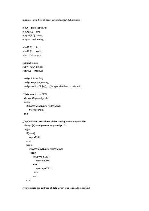
module syn_fifo(clk,reset,wr,rd,din,dout,full,empty);input clk,reset,wr,rd;input[7:0] din;output[7:0] dout;output full,empty;wire[7:0] din;wire[7:0] doubt;wire full,empty;reg[2:0] wp,rp;reg w_full,r_empty;reg[7:0] fifo[7:0];assign full=w_full;assign empty=r_empty;assign doubt=fifo[rp]; //output the data rp pointed//data wire in the FIFOalways @ (posedge clk)beginif ((wr==1'b0)&&(w_full==1'b0))fifo[wp]<=din;end//wp(indicate then adress of the coming new data)modified always @(posedge reset or posedge clk)beginif(reset)wp<=1'b0;elsebeginif((wr==1'b0)&&(w_full==1'b0))beginif(wp==3'b111)wp<=3'b000;elsewp<=wp+1'b1;endendend//rp(indicate the address of data which was readout) modefiedalways @(posedge reset or posedge clk)beginif(reset)rp<=3'b111;elsebeginif((rd==1'b0)&&(r_empty==1'b0))beginif(rp==3'b111)rp<=3'b000;elserp<=rp+1'b1;endendend//generate 'empty' indicationalways @(posedge reset or posedge clk)beginif(reset)r_empty=1'b1;elsebeginif(((rd==1'b0)&&(wr==1'b1))&&((rp==wp-3'b010)||((rp==3'b111)&&(wp==3'b001))||((rp==3'b11 0)&&(wp==3'b000))))r_empty<=1'b1;else if((r_empty==1'b1)&&(wr==1'b0))r_empty<=1'b0;endend//generate 'full' indicationalways @(posedge reset or posedge clk)beginif(reset)w_full<=1'b0;elsebeginif((rp==wp)&&(wr==1'b0)&&(rd==1'b1))w_full<=1'b1;else if((w_full==1'b1)&&(rd==1'b0))w_full<=1'b0;endend endmodule。
FIFO同步、异步以及Verilog代码实现
FIFO同步、异步以及Verilog代码实现FIFO 很重要,之前参加的各类电⼦公司的逻辑设计的笔试⼏乎都会考到。
FIFO是英⽂First In First Out 的缩写,是⼀种先进先出的数据缓存器,他与普通存储器的区别是没有外部读写地址线,这样使⽤起来⾮常简单,但缺点就是只能顺序写⼊数据,顺序的读出数据, 其数据地址由内部读写指针⾃动加1完成,不能像普通存储器那样可以由地址线决定读取或写⼊某个指定的地址。
FIFO⼀般⽤于不同时钟域之间的数据传输,⽐如FIFO的⼀端是AD数据采集, 另⼀端是计算机的PCI总线,假设其AD采集的速率为16位 100K SPS,那么每秒的数据量为100K×16bit=1.6Mbps,⽽PCI总线的速度为33MHz,总线宽度32bit,其最⼤传输速率为 1056Mbps,在两个不同的时钟域间就可以采⽤FIFO来作为数据缓冲。
另外对于不同宽度的数据接⼝也可以⽤FIFO,例如单⽚机位8位数据输出,⽽ DSP可能是16位数据输⼊,在单⽚机与DSP连接时就可以使⽤FIFO来达到数据匹配的⽬的。
FIFO的分类根均FIFO⼯作的时钟域,可以将FIFO分为同步FIFO和异步FIFO。
同步FIFO是指读时钟和写时钟为同⼀个时钟。
在时钟沿来临时同时发⽣读写操作。
异步FIFO是指读写时钟不⼀致,读写时钟是互相独⽴的。
FIFO设计的难点 FIFO设计的难点在于怎样判断FIFO的空/满状态。
为了保证数据正确的写⼊或读出,⽽不发⽣益处或读空的状态出现,必须保证FIFO在满的情况下,不 能进⾏写操作。
在空的状态下不能进⾏读操作。
怎样判断FIFO的满/空就成了FIFO设计的核⼼问题。
.........................................................................................................................................同步FIFO的Verilog代码之⼀在modlesim中验证过。
verilog FIFO序列(深度可调)
公司招聘时给大家出的题目,我自己也给做了一下,帮助大家学习。
主程序和tb文件都在。
可用modelsim直接仿真。
主程序:module fifo(datain,clk,reset,dataout,wr,rd,full,empty);input[7:0]datain;input clk,reset,rd,wr;output[7:0]dataout;output full,empty;reg[7:0]dataout;reg rp,wp;reg[3:0]counter;reg[7:0]ram[15:0];wire full,empty;always@(posedge clk)if(!reset)beginrp=0;wp=0;counter=0;dataout=0;endelsecase({rd,wr})2'b00:counter=counter;2'b01:beginif(!full)beginram[wp]=datain;counter=counter+1;wp=(wp==15)?0:wp+1;endendif(!empty)begindataout=ram[rp];counter=counter-1;rp=(rp==15)?0:rp+1;endend2'b11:beginif(counter==0)dataout=datain;elsebeginram[wp]=datain;wp=(wp==15)?0:wr+1;dataout=ram[rp];rp=(rp==15)?0:rp+1;endendendcaseassign full=(counter==5);assign empty=(counter==0); endmodule测试文件(testbench):`timescale1ns/1nsmodule fifo_tb;reg reset,clk,wr,rd;reg[7:0]datain;wire[7:0]dataout;wire full,empty;always#50beginclk=~clk;datain={$random}%256;endinitialbeginreset=0;clk=0;{rd,wr}=2'b00;#100reset=1;{rd,wr}=2'b01;#2000{rd,wr}=2'b10;#2000{rd,wr}=2'b11;#500$stop;endfifom0(.datain(datain),.clk(clk),.reset(reset),.dataout(dataout),.wr(wr),.rd(rd),.full(full),.empty(empty)) ;endmodule。
异步FIFO的verilog代码实现(包含将满和将空逻辑)

异步FIFO的verilog代码实现(包含将满和将空逻辑)异步FIFO的verilog代码实现(包含将满和将空逻辑)代码参考来源:1. Clifford E. Cummings, "Simulation and Synthesis Techniques for Asynchronous FIFO Design".2.⽬录异步FIFO简介使⽤场景:在有⼤量的数据需要进⾏跨时钟域传输,并且对数据传输速度要求⽐较⾼的场合。
⼀个异步 FIFO ⼀般由如下部分组成:1. Memory, 作为数据的存储器;2.写逻辑部分,主要负责产⽣写信号和地址;3.读逻辑部分,主要负责产⽣读信号和地址;4.地址⽐较部分,主要负责产⽣ FIFO 空、满的标志。
跟普通的FIFO相⽐,异步FIFO实际上多了读写地址的跨时钟域同步的逻辑,以及两个时钟域中读写信号的⽐较逻辑。
异步FIFO关键技术1 -- 读写信号跨时钟域同步⾸先,FIFO的关键是需要判断读空和写满,⽽这两个信号的产⽣依赖读地址和写地址。
在异步FIFO中,读和写是分在两个时钟域中的,在写时钟域,需要得到读地址的信息进⽽判断是否写满(写指针是否追上读指针),同理,在读时钟域,也需要写地址的信息。
我们知道跨时钟域的单⽐特数据⼀般可以⽤双寄存器法进⾏同步,但读写地址通常都是多⽐特的信号,此时如何进⾏同步呢?当然,多⽐特的同步肯定可以通过增加握⼿信号来解决,但实际上对于数值上连续的信号,可以采⽤格雷码进⾏多⽐特到单⽐特的传输。
格雷码再次不做介绍,具体原理可以参考:有了格雷码,就可以将读写地址同步到各⾃的时钟域了。
异步FIFO关键技术2 -- 读写地址的⽐较跟普通fifo⼀样,异步fifo也是通过⽐较读写地址是否相同来判断当前fifo是否空满。
区别在于,异步FIFO因为使⽤了格雷码对地址进⾏编码传输。
⽐如读信号通过格雷码编码后同步到写时钟域,此时需要只需要写信号对应的格雷码和读信号格雷码是否相同(有效位相同)。
- 1、下载文档前请自行甄别文档内容的完整性,平台不提供额外的编辑、内容补充、找答案等附加服务。
- 2、"仅部分预览"的文档,不可在线预览部分如存在完整性等问题,可反馈申请退款(可完整预览的文档不适用该条件!)。
- 3、如文档侵犯您的权益,请联系客服反馈,我们会尽快为您处理(人工客服工作时间:9:00-18:30)。
对于FIFO,读写指针都指向一个内存的初始位置,每进行一次读写操作, 相应的指针就递增一次,指向下一个内存位置。当指针移动到了内存的最后 一个位置时,它又重新跳回初始位置。在FIFO非满或非空的情况下,这个过 程将随着读写控制信号的变化一直进行下去。如果FIFO处于空的状态,下一 个读动作将会导致向下溢(underflow),一个无效的数据被读人;同样,对于 一个满了的FIFO,进行写动作将会导致向上溢出(overflow),一个有用的数据 被新写入的数据覆盖。这两种情况都属于误动作,因此需要设置满和空两个 信号,对满信号置位表示FIFO处于满状态,对满信号复位表示FIFO非满,还 有空间可以写入数据;对空信号置位表示FIFO处于空状态,对空信号复位表 示FIFO非空,还有有效的数据可以读出。
write_word (16'h0001); write_word (16'h0002); write_word (16'h0003); write_word (16'h0004); write_word (16'h0005); write_word (16'h0006); write_word (16'h0007); write_word (16'h0008); repeat (6) begin read_word; end end endtask
initial begin clk = 0; forever begin #10 clk = 1; #10 clk = 0; end end
initial begin //test1; test2; //调用测试模块2 end
task test1; begin din = 16'hzzzz; writep = 0; readp = 0; rstp = 1; #50 rstp = 0; #50; write_word (16'h1111); write_word (16'h2222); write_word (16‘h3333); //写入3个数据 read_word; read_word; //读两个 write_word (16‘h4444); //在写一个数据 repeat (6) begin read_word; end
always @(posedge clk) begin if (rstp == 1'b1) begin tail <= 2‘b00; //复位 end else begin if (readp == 1'b1 && emptyp == 1'b0) begin tail <= tail + 1; end end end always @(posedge clk) begin if (rstp == 1'b1) begin count <= 2'b00; end else begin case ({readp, writep}) 2'b00: count <= count; 2'b01: if (count != MAX_COUNT) count <= count + 1; //为写状态时计数器进行加法计数 2'b10: if (count != 2'b00) count <= count - 1; //为读状态计数器进行减法计数 2'b11: count <= count; endcase end end
endmodule
测试程序:
module test_fifo; reg reg reg [15:0] reg reg wire [15:0] wire wire clk; rstp; din; readp; writep; dout; emptyp; fullp;
reg [15:0] value; fifo U1 (.clk(clk),.rstp(rstp),.din(din),.readp(readp),.writep(writep),.dout(dout), .emptyp(emptyp),.fullp(fullp));
FIFO存储器的设计 module fifo (clk, rstp, din, writep, readp, dout, emptyp, fullp); input clk; input rstp; //复位信号 input [15:0] din; input readp; //读信号 input writep; //写信号 output [15:0] dout; output emptyp; //空标志 output fullp; //满标志 parameter DEPTH = 2, MAX_COUNT = 2‘b11; //定义地址最大值 reg emptyp; reg fullp; reg [15:0] dout; reg [(DEPTH-1):0] tail; //定义读指针 reg [(DEPTH-1):0] head; //定义写指针 // 定义计数器 reg [(DEPTH-1):0] count; reg [15:0] fifomem[0:MAX_COUNT]; //定义fifomem存储器有4个16位的存储器
always @(count) begin if (count == 2'b00) emptyp <= 1‘b1; //count为0时emptyp赋为1 else emptyp <= 1'b0; end
always @(count) begin if (count == MAX_COUNT) fullp <= 1‘b1; //计数到最大时fullp赋为1 else fullp <= 1'b0; end
//读数据 begin forever begin @(negedge clk); if (emptyp == 1'b0) begin read_word; end #50; end end join end endtask
endmodule
// dout被赋给tail指向的值 always @(posedge clk) begin if (rstp == 1) begin dout <= 16‘h0000; //复位信号有效置0 end else begin dout <= fifomem[tail]; //将fifomem中第tail个单元赋给dout end end always @(posedge clk) begin if (rstp == 1'b0 && writep == 1'b1 && fullp == 1'b0) begin fifomem[head] <= din; //写入 end end always @(posedge clk) begin if (rstp == 1'b1) begin head <= 2‘b00; //复位 end else begin if (writep == 1'b1 && fullp == 1'b0) begin head <= head + 1; end end end
task test2; reg [15:0] writer_counter; begin writer_counter = 16'h0001; din = 16'hzzzz; writep = 0; readp = 0; rstp = 1; #50 rstp = 0; #50; fork //写数据 begin repeat (500) begin @(negedge clk); if (fullp == 1'b0) begin write_word (writer_counter); #5; writer_counter = writer_counter + 1; end #50; end end
实验四 复杂逻辑电路设计
实验室:九教南212
实验内容 (1)FIFO存储器的设计 (2)熟悉modelsim设计环境
FIFO是英文First In First Out 的缩写,是一种先进先出的数据缓存器,他与普通存
储器的区别是没有外部读写地址线,这样使用起来非常简单,但缺点就是只能顺序写
入数据,顺序的读出数据,其数据地址由内部读写指针自动加1完成,不能像普通存 储器那样可以由地址线决定读取或写入某个指定的地址。 FIFO的一些重要参数 FIFO的宽度:也就是英文资料里常看到的THE WIDTH,它指的是FIFO一次读写操 作的数据位,就像MCU有8位和16位,ARM 32位等等。 FIFO的深度:THE DEEPTH,它指的是FIFO可以存储多少个N位的数据(如果宽 度为N)。如一个8位的FIFO,若深度为8,它可以存储8个8位的数据,深度为12 , 就可以存储12个8位的数据。 满标志:FIFO已满或将要满时由FIFO的状态电路送出的一个信号,以阻止FIFO的
写操作继续向FIFO中写数据而造成溢出(overflow)。
空标志:FIFO已空或将要空时由FIFO的状态电路送出的一个信号,以阻止FIFO的 读操作继续从FIFO中读出数据而造成无效数据的读出(underflow)。
读指针:指向下一个读出地址。读完后自动加1。
写指针:指向下一个要写入的地址的,写完自动加1。
task read_word; begin @(negedge clk); readp = 1; @(posedge clk) #5; readp = 0; end endtask task write_word; input [15:0] value; begin @(negedge clk); din = value; writep = 1; @(posedge clk); #5; din = 16'hzzzz; writep = 0; end endtask