日本东京精密
仪器设备行业分类及销售注意事项
精密仪器使用行业分类本公司涉及项目仪器分类:1.精密测量类2.理化分析类3.力学实验类仪器使用行业大概分类:精密测量仪器类(测量长度和形状)1.2.三坐标机加工企业:汽车零部件,工程机械,农业机械,各种产品加工,模具行业,铸造行业,锻造行业,技术监督局,给大厂配套企业.A. 针对产品类型:箱体零件,精密轴承,要求高的零件,特别行为公差要求要的都必须要上三坐标检测,三坐标是一个通用型的测量设备,他满足了几乎所有的检测项目,比如圆度,圆柱度,轮廓度,平面平行度,直线度,圆锥度,垂直度,对称度,角度,位置度,同轴度,同心度,轴向跳动,径向跳动,轴全项跳动,径向全跳动。
B. 加上CAD数模功能,让三坐标的功能发挥到了淋漓尽致,数据返回CAD,修正加工,未知零件检测,数据与软件反求有机结合,实现复杂未知零件的逆向工程。
C. 加上影像测量头可实现工件的快速检测,适合大批量全检工件,精度可大三坐标精度,甚至更高。
D. 品牌定位及知识:进口品牌—日本三丰,德国卡尔蔡司,瑞典海克斯康,德国温泽,美国法如,意大利柯德三,国产品牌—青岛海克斯康,深圳思瑞,青岛雷顿,青岛麦科三维,西安爱德华等。
2.圆柱度仪:圆柱度是一款检测圆形零件的高精度设备,和三坐标对比,她们共同的特点是都能检测圆柱度,但是检测精度相差甚远,不能放在一个层面上对比。
因此圆柱度仪是一款专业设备,非通用设备。
圆柱度仪可检测内容有:圆度,圆柱度,同心度,同轴度,平面度,平行度,垂直度,经向偏差,厚度偏差,径向跳读,径向全跳动,直径测量,直线度,倾斜度,锥度,直径轮廓公差,直线轮廓公差,宽度测量,功率谱,谐普分析,轮廓操作,圆锥面分析。
这些检测项目适合能够放在设备平台上的所有零件,不一定是圆形规则的。
A.B.针对的特殊行业:液压阀生产企业,液压缸生产企业,轴承.滚子行业,电动机生产企业,气缸套生产企业,活塞生产企业,蜗轮增压生产企业,电主轴生产企业等C.D.针对的特殊装配情况:对于装配过程中需要启到轴和孔有配合要求,比如说防水,防油,防渗出类的E.F.品牌定位及知识:进口品牌—英国泰勒,瑞士TESA,德国马尔,德国霍梅尔,日本三丰,东京精密,小板。
常用丝杠品牌

常用丝杠品牌一、引言丝杠作为机械传动装置中常见的一种,广泛应用于各个行业的机械设备中。
常用丝杠品牌的选择对于机械设备的性能和可靠性具有重要影响。
本文将介绍几个常用丝杠品牌,并对其特点、应用领域以及性能进行详细分析。
二、THK(日本东京精密)THK是一家全球知名的丝杠品牌,总部位于日本东京。
该品牌以其高精度、高可靠性和长寿命而闻名于世。
THK的丝杠产品广泛应用于机床、自动化设备、半导体设备等领域。
其产品特点包括低噪音、低磨擦、高刚性等。
THK的丝杠产品采用先进的创造工艺和材料,确保了其在各种工况下的稳定性和可靠性。
三、HIWIN(台湾汇翼)HIWIN是台湾汇翼机械股分有限公司的品牌,是世界率先的线性运动控制系统供应商之一。
HIWIN的丝杠产品广泛应用于机床、机器人、半导体设备等领域。
该品牌的丝杠产品具有高精度、高刚性和高负载能力的特点。
HIWIN的丝杠产品采用先进的滚珠丝杠技术,具有低磨擦、低噪音和长寿命等优势。
四、KSS(德国KSS)KSS是德国KSS KUHNLE, KOPP & KAUSCH AG的品牌,是世界率先的丝杠创造商之一。
KSS的丝杠产品广泛应用于航空航天、汽车创造、医疗设备等高精度领域。
该品牌的丝杠产品具有高精度、高刚性和高可靠性的特点。
KSS的丝杠产品采用先进的创造工艺和材料,确保了其在各种恶劣环境下的稳定性和可靠性。
五、Rexroth(德国力士乐)Rexroth是德国力士乐集团的品牌,是全球率先的工业技术供应商之一。
Rexroth的丝杠产品广泛应用于机床、自动化设备、物流系统等领域。
该品牌的丝杠产品具有高精度、高刚性和高负载能力的特点。
Rexroth的丝杠产品采用先进的滚珠丝杠技术,具有低磨擦、低噪音和长寿命等优势。
六、SKF(瑞典斯凯孚)SKF是瑞典斯凯孚集团的品牌,是全球率先的轴承和密封件创造商之一。
SKF 的丝杠产品广泛应用于工业设备、汽车创造、航空航天等领域。
闪存芯片低温测试中的制冷技术蔡瑾马晓营
闪存芯片低温测试中的制冷技术蔡瑾马晓营发布时间:2022-04-10T00:44:10.842Z 来源:《探索科学》2022年1月上作者:蔡瑾马晓营[导读] 近年来,社会进步迅速,我国的智能化建设的发展也有了改善。
恩智浦半导体(天津)有限公司蔡瑾马晓营天津市摘要:近年来,社会进步迅速,我国的智能化建设的发展也有了改善。
随着互联网、大数据、云计算和物联网等产业的快速发展,存储器芯片在整个集成电路产业链中扮演着极为重要的角色。
我国的存储器芯片,在很长一段时间内基本依赖于进口。
近几年来得益于国家对于集成电路产业的不断重视与扶持,存储器芯片的国产化开始逐步崛起。
关键词:闪存芯片;低温测试;制冷技术引言固态硬盘采用闪存芯片作为存储介质,相比于以碟片为存储介质的机械硬盘,具有更高的读写性能。
因此固态硬盘逐渐成为各种计算机的主流存储设备,被广泛应用到从嵌入式设备、个人计算机到高性能计算机等系统之中。
但是目前其单盘容量还是远小于磁盘。
为提高固态硬盘的存储容量,闪存芯片制造商致力于开发多级闪存以及3D堆叠技术。
其中,多级闪存技术使得单个闪存单元中能够存储多比特数据;而3D堆叠技术则通过纵向扩展闪存芯片以增加闪存单元的体密度。
然而多级闪存技术的使用也降低了闪存的可擦写次数和增加了闪存的读写延时;3D堆叠技术也导致闪存的写入方式发生重大改变。
因此,针对新型高密度固态硬盘,通过挖掘其内在特性优化其寿命和性能,具有重要的学术意义和广泛的应用前景。
1数字模型的缺陷闪存芯片是一种数模混合的产品,如果使用SPICE或者FastSPICE仿真,芯片功能会完整保留,但仿真速度会很慢,影响整个产品的验证进度。
基于Verilog的数字模型仿真是一种快速选择。
但是传统的Verilog仿真无法在内部模块之间传递模拟信号,所以只能用数字信号来表征模拟行为。
如图1所示,一个简单的电压传输电路需要在6V和7V之间选择传递,如果使用数字模型,那么输出端口无法区分电压的来源。
日本精工NSK株式会社
日本精工NSK株式会社一,简介;日本精工株式会社(にほんせいこう、NSK Ltd. ),在其核心轴承产业日本排名第一,世界排名第三。
公司本总部位于日本东京都品川区大崎一丁目,公司简称NSK。
隶属于日本みずほ财团。
成立于1916年,是日本国内第一家设计生产轴承的厂商。
几十年来,NSK开发出无数新型轴承,满足世界各地用户的需求,并为产业发展和技术进步做出了极大的贡献。
同时NSK凭借其在精密加工方面的技术优势,不断开发汽车零部件、精密机械组件等高、精、尖产品,在电子应用等领域积极开展多元化经营。
经过20多年的潜心经营,NSK已经在发达的欧美地区建立了成熟的生产、开发和销售机制。
在亚太地区,由于卓越的品质及周到的服务,NSK的事业也进展迅猛。
二,主要产品;NSK在滚珠轴承、汽车用轴承、滚珠丝杠的市场占有率都是全世界第一。
NSK在全球20多个国家和地区建立了销售网络,并拥有30多家工厂,行业排名在世界范围内稳居榜首。
为了感谢中国广大用户的信赖,NSK致力于向经济持续高速发展的中国输出先进的生产技术和管理经验,逐步确立并完善以生产为核心、技术为指导、营销信息为辅助的三位一体化事业体制,NSK将加快这一体制的本地化进程,从而为中国的广大用户提供更直接、更完善的服务,为中国的产业现代化作出应有的贡献。
NSK的主要产品是轴承,它是所有机器的基础;是现代社会中不可缺少的产品;素有"机械产业的粮食"之美称;它确保所有工业产品的质量;NSK的宗旨在于运行与控制;对机器的运转/摩擦现象寻根究底,以确保旋转和运作的平稳;它无时不在,时刻为人类提供着丰富多彩的生活并将对全球性的节能运动和资源保护作出贡献日本精工株式会社(NSK LTD.简称NSK)成立于1916年,是日本国内第一家设计生产轴承的厂商。
几十年来,NSK开发出无数新型轴承,满足世界各地用户的需求,并为产业发展和技术进步做出了极大的贡献。
同时NSK凭借其在精密加工方面的技术优势,不断开发汽车零部件、精密机械组件等高、精、尖产品,在电子应用等领域积极开展多元化经营,精工SII作为精工株式会社会社的子公司,其生产的晶振是精工seiko,除了做电子元器件,精工也是世界上著名的石英手表厂商,同时也生产电脑打印机。
表面粗糙度培训教材(东京精密)
λ =h σ
σ: 复合粗糙度
σ = Rq12 + Rq22
Large roughness
Wear or damage
油膜 & 粗糙度 9
滑动摩擦力 & 粗糙度
• 滑动表面接触在少数微小的点上
■ 巨大的应力 ■ 支撑在接触点上 ■ 滑行运动在两表面间产生
摩擦力
■ 滑行轨道的特性 ● 提高硬度较少磨损 ● 降低 Rz以较少峰点间的应力集中度
Appearance area A
实际接触区域 ai
10
如何测量粗糙度?
1比较法 将被测表面与标有一定评定参数值的表面粗糙度样板比较 从判断被测表面的粗糙度。 2光切法 应用光切原理测量表面粗糙度的一种测量方法。按光切原 理制成的仪器叫做光切显微镜。这种方法用来测量Rz。 3干涉法 利用光波干涉原理测量表面粗糙度的一种方法。按干涉原 理制成的仪器叫做干涉显微镜,一般用来测量粗糙度值要 求低的表面 4针描法 接触式测量表面粗糙度的方法,最为常见。
Surfcom - 仪器结构
立柱
与工件竖直宽度垂直 Z轴
X轴
来回移动
驱动部
工件实表面
测针
放大器
测针顶端形状
θ rtip
θ= 60°(or 90°) r tip = 2μm (or 5,10μm)
工件
夹具 / 定位
测针 (Pickup)
LVDT (模拟) 测针压力 : 0.75mN
(测针顶端为0.2 μm)
粗糙度的参数
主要参数说明
间距参数
n
(1) S:轮廓单峰平均间距
S = ∑ Sn 1
(JIS B0601:’82)
n
i =1
三坐标(三次元)租赁
三坐标(三次元)租赁三坐标(三次元)租赁,以租赁代替购买来控制企业成本,这种在外企中十分流行的管理方式,正慢慢受到国内中小企事业单位的青睐。
三坐标(三次元)租赁是指将设备的资产使用权从拥有权中分开,出租人具有资产所有权,承租人拥有资产使用权,出租人与承租人签订租赁合同,以交换使用权利的一种交易形式。
三坐标(三次元)租赁是指在约定时间内,租赁经营人将租赁设备交付承租人使用,三坐标(三次元)租赁的实质是在将租赁设备的产权与使用权分开的基础上,通过出租的使用权而获取收益的一种经营行为。
按照不同的分类标准,租赁具有不同的分类方法,常见的有按照租赁期长短划分和按照经营目的划分两类。
1997年颁布实施的《租赁试点工作暂行管理办法》在实际经营中,一般认为15天以下为短期租赁,15~90天为中期租赁,90天以上为长期租赁。
长期租赁,是指租赁企业与用户签订长期(一般以年计算)租赁合同,按长期租赁期间发生的费用。
短期租赁,是指租赁企业根据用户要求签订合同,为用户提供短期内(一般以日、月计算)的服务,收取短期租赁费,解决用户在租赁期间的各项服务要求的租赁形式。
按照经营目的划分融资租赁。
融资租赁是指承租人以取得设备的所有权为目的,经营者则是以租赁的形式实现标的物所有权的转移,其实质是一种带有销售性质的长期租赁业务,这种租赁的支付模式其实就是一个首付款和每个月月供,可以帮助客户留有足够的周转资金用来经营,而且租赁公司都可以开17%增值税发票。
客户都可以进行抵扣。
目前的三坐标品牌大概有:日本三丰MITUTOYO,日本东京精密ACCRETECH, 德国蔡司ZEISS,瑞士TESA,德国温泽WENZEL,德国马尔MAHR,德国WERTH,意大利DEA,美国ST,意大利COORD3,意大利POLI,意大利ITF,瑞士TRIMOS,英国LK,英国STARETT,英国ABLINK,英国IMS,比利时METRIS,德国霍梅尔HOMMEL,美国OGP,国产的品牌有海克斯康,青岛雷顿,青岛佛迪,智泰,新天光电,上海光学仪器等等,。
化学机械抛光(CMP)设备市场概况

数据来源:公开资料,赛迪顾问整理图1 半导体制造设备表图2 2018年全球半导体设备各区域销售额(单位:百万美元) 2019.5图3 2018年全球半导体设备产品结构(单位:百万美元)图4 2018年全球晶圆制造设备市场规模(单位:百万美元) 2019.5的供应商美国应材的市场份额依然呈现逐年递增的态势[3]。
尽管美国应材公司进入CMP 设备领域比较晚(其第一台CMP Mirra 产品是1997年推出的),但该公司能在非常短的时间内占领大部分市场。
作为世界上最大的半导体加工设备公司,应材凭借其世界服务和性能保证资源优势,从以前CMP 设备市场领先的SpeedFam 、Westech(IPEC)公司赢得了市场。
IPEC 和SpeedFam(曾一度是CMP 设备的第一和第二供货厂家)在应材公司和荏原公司的竞争中变得萎缩了。
荏原是紧随应材之后的CMP 第二,该公司获得了亚洲市场的大部分,是日本和台湾地区市场的CMP 设备最大供货商。
参考文献[1]半导体制造工艺流程及其需要的设备和材料[R/OL].(2018-05-25)./anli/13/61440.html[2]化学机械抛光在精密加工和超精密加工领域的应用[R/OL].(2017-06-30).https:///a/153293442_99913194[3]Challenges & Opportunities in post CMP Cleans Innovation[R/OL].(2018-04-09).https:///wp-content/uploads/2018/04/Michael-Wedlake-Business-of-Cleans.pdf数据来源:三星,赛迪顾问图5 2018年全球CMP设备市场区域结构图6 全球CMP设备市场规模及品牌结构(单位:百万美元)。
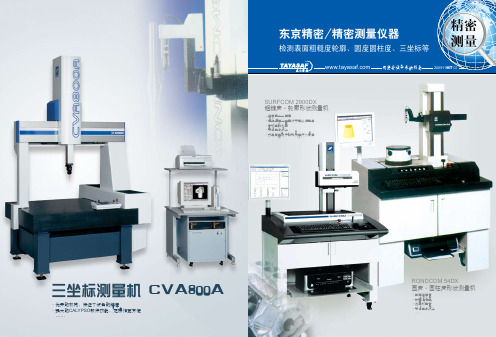
东京精密
设备采购指南·系列
目 录
Contents
01
表面粗糙度测量仪
HANDYSURF E-35B, E-40A, E-45A便携式表面粗糙度测量机 SURFCOM 480A/130A 表面粗糙度测量机 SURFCOM 1400D 表面粗糙度测量机 SURFCOM 1400-3DF 精密表面粗糙度测量机 SURFCOM 1400D-LCD 玻璃波纹度测量机 SURFCOM 1400-PDP 形状测量机
上海热线:021-54248686
表面粗糙度测量仪
表面粗糙度测量机 SURFCOM 480A/130A
可操作性强:
·TFT大屏幕液晶触摸屏,简单实用 ·AI功能,操作简单,减少操作失误 ·世界各国通用 ·满足各种需求的分析功能 ·自动停止功能(针对SURFCOM 480A) ·测量向导功能 ·个性化图标设计,方便操作 ·再计算功能降低了测针磨损,
传真:021-64418200
传真:00852-81673379
地址:上海市徐汇区宛平南路521号 地址:香港上环文咸东街65-67号
恒昌花园B座903室
喜利商业大厦15楼
上海热线:021-54248686
设备采购指南·系列
TAYA S A F
高斯、2RC λс:0.08、0.25、0.8、2.5mm、λs:2.5、8μm
评价 固定模式 长度 任意模式
截止波长值×5
0.4~12.5mm(0.1mm单位)
0.4~4.0mm (0.1mm单位)
测量速度
0.6mm/s(返回1mm/s)
0.3mm/s (返回0.5mm/s)
东京精密三次元使用技术手册
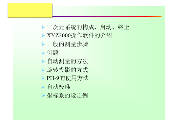
¾系统的组成一、各部件的名称:三次元坐标测量机二、XYZ2000操作软件介绍*快捷方式**进入联机**选择GEM *测量数据的表示方法:1,直角坐标的表示方法。
测定点用X、Y、Z、坐标表示。
2,圆柱坐标的表示方法。
测定点用AXY(角度)、Z表示,根据平面不同而变化。
三、一般的测量顺序1)系统的启动(P1)。
•自动校正手顺¾补助处理→自动校正(元 FAMILY TREE导轨面导轨面、开机手顺:4.1 打开UPS(图1)的电源开关,然后打开冷却空气机(图2)。
P 图6U图10、关机手顺:5.1先退出操作画面(图图15PC主机开关控制开关拧到OFF三个月Y轴内的气动轴的走行面(光尺的上面和侧面)的污物。
目视1)取下Y轴的外壳用有机溶剂(无水酒精等)擦拭干净。
2)少量的灰尘用柔软的抹布擦拭。
3)光尺上的脏物要小心除去。
六个各轴(X、Y、Z、)光尺上的脏污。
目视1)各轴光尺侧的外壳取下(方法见附页)。
2)用脱脂棉沾少量的丙酮或酒精,轻轻的擦拭。
在擦拭的过程必须小心慎重,防止擦伤。
三次元日常保养要领7、一般测量手顺4) 校正测头 测头NO:在校正球上测量5点以上后按终止键(第一坐标系设定完毕)5)基准面设定A面上测量3点以上后按终止6) 原点设定B孔中测量3点以上后按终止7) 基准轴设定C孔中测量3点以上后按终止﹏以上5)7)步骤操作完后第二坐标系设定完毕8) 测量D孔测量3点以上后按终止「X=50 Y=30」9) 系统的终止(P4参照)ENTE功能菜单机能处理7—2 电子显微镜和ITV照相机系统的测量使用方法1) 系统的启动(P1参照)2) 把校正球和测量物固定在平台上。
3) 选择测量再开始。
(A49)4) 几何形状自动判别(AI机能)OFF5)测量平面的固定ENTE6)测头直径的变更测头直径:07)原点设定“十”线在A孔的四周测量3点以上后按终止8)基准轴设定“十”线在B孔的四周测量3点以上后按终止以上7﹏)8)步骤操作完后第二坐标系设定完毕9)测量“十”线在C孔的四周测量3点以上后按终止“十”线在D边上测量1点后按终止10)系统的终止(P4参照)8·机能处理机能处理测量功能处理是在测量处理执行过程中和自动测量处理执行过程中插入执行处理处理和内容如下处理代码F0手动方式测量的场合。
三坐标测量仪厂家-三坐标测量仪器厂家【品牌大全】
三坐标测量厂家,三坐标测量仪器厂家,三坐标测量仪品牌内容来源网络,由深圳机械展收集整理!更多三坐标测量仪器展览展示,就在深圳机械展的测量展区!三坐标测量机,又叫三次元。
三坐标测量厂家、三坐标测量仪器厂家,三坐标测量品牌很多,网上找,但部分(如测量杆,测量头及光栅尺)很多都是进口的,生产三坐标的厂家有德国蔡司,海克斯康、捷克博测量技术等。
测量仪器的概念其内容包括:精度、误差、测量标准器材、长度测量、角度测量、形状测量、传统光学仪器。
在精密测量上的应用等等。
生活、生产都要用到测量仪器,测绘工作离不开各种测量仪器,测量仪器行业覆盖食品安全、环境保护、石油化工、电子电器、药物研发、4G无线通信技术、航空航天等产业等领域,成为近年来发展快的仪器仪表电子行业之一。
三坐标测量厂家,三坐标测量仪器厂家,三坐标测量仪品牌1 海克斯康HEXAGON(海克斯康测量技术(青岛)有限公司)2 雷顿Leader(从事三坐标测量机等精密测量设备研发生产与技术服务的中美合资企业,青岛雷顿数控测量设备有限公司)3 温泽Wenzel(德国温泽集团旗下分公司,计量解决方案制造商之一,跨国公司,温泽测量仪器(上海)有限公司)4 卡尔蔡司(始创于1890年德国,光学仪器制造企业之一,蔡司光学仪器(上海)国际贸易有限公司)5 三丰Mitutoyo(于1934年日本,跨国公司,致力于各种精密测量仪器研发生产销售的企业,三丰精密量仪(天津)有限公司)6 东京精密Accretech(始创于1949年日本,致力于个性领域的精密机械仪器研发、生产的企业,东精精密设备(上海)有限公司)7 爱德华(中国坐标测量机制造企业之一,外商企业,西安爱德华测量设备股份有限公司)8 德仁Dukin(韩国独资企业,从事三坐标的研制、生产、销售及服务的技术企业,济南德仁三坐标测量机有限公司)9 思瑞Serein(从事研发生产精密坐标测量机/影像测量仪/测高仪等计量设备的企业,思瑞测量技术(深圳)有限公司)10 奥秋(组建于2005年,致力于各种精密测量仪器研发生产销售的企业,上海奥秋精密仪器有限公司)三坐标测量厂家——苏州精坐标测量技术有限公司精坐标测量技术(苏州)有限公司是研发,生产和销售精密量测仪器的公司,是一家源于德国的三坐标生产厂家。
三坐标测量仪什么牌子好
三坐标测量仪什么牌子好?三坐标测量仪十大品牌随着现代制造业不断发展,企业对机械制造产品的精密度要求越来越高,用于工业检测、质量控制等领域的三坐标测量仪在汽车、航空航天及国防等众多行业得到广泛应用。
越来越多的机械加工企业开始关注三坐标测量这项重要工序。
三坐标测量仪三轴均有气源制动开关及微动装置,可实现单轴的精密传动;数据采集系统采用高性能手动三坐标专用系统,可靠性好。
今天,小编精选了十个全球知名的三坐标测量仪器品牌,看看他们是如何完成精密测量。
一、ZEISS蔡司始于1846年德国,是全球领先的光学、精密工程及电子观测制造商,在光学及光电子学领域处于领先地位的全球性国际化公司。
1973年蔡司就已经成功制造世界上第一台CNC三坐标测量机-UMM500。
同时蔡司不断开发新技术与推出新产品,到现在为止已拥有多个国际专利。
在中高端市场,每年销售额占全球市场占有量的三分之一。
蔡司测量机在航空、航天、汽车、电子、机械与塑料等多个行业中得到广泛的使用。
二、HEXAGON海克斯康创建于1975年瑞士,其测头技术在机床工具行业享有盛名。
海克斯康测量技术主要包括两个部分:“大尺寸计量”,主要包括山体测量、城市测绘、道路干线、隧道桥梁、以及其它建筑工程的的测量。
“小尺寸计量”,关注更加精密的尺寸测量任务,面向制造业提供的各种产品,包括汽车、航空航天、机床、军工、加工制造以及日用消费品。
三、Mitutoyo三丰日本著名测量仪品牌,全球测量方案和测量设备专业提供商,专注于测量方案和测量设备的全球性公司,在整个量具行业独占鳌头。
主要产品包括:量具行业的各个项目,包括:千分尺、卡尺、深度尺、内径千分尺、千分表、杠杆千分表、高度尺、微分头、量块、线性测微器、光栅尺、粗糙度仪、轮廓测量仪、显微镜、硬度计、三坐标测量机等。
四、Wenzel温泽德国温泽集团是计量领域创新的先驱。
温泽多样化的产品提供了三维测量、计算机断层扫描、光学高速扫描等多个行业的独特解决方案。
12刀位星型电动刀塔的设计(有完整图纸)
目录1.绪论 (4)1.1毕业设计的背景及目的 (4)1.2刀塔概况及发展趋势 (4)1.2.1刀塔概况 (5)1.2.2刀塔发展趋势 (5)1.3现代数控机床的特点及发展趋势 (6)1.3.1现代数控机床的特点 (6)1.3.2现代数控机床的发展趋势 (8)1.3.3现代技术给机床业带来的新动向 (10)2.刀塔的设计及计.................... 错误!未定义书签。
2.1刀塔的功能,类型和应满足的要求.......................... 错误!未定义书签。
2.1.1机床刀塔的功能..................................................... 错误!未定义书签。
2.1.2机床刀塔的类型..................................................... 错误!未定义书签。
2.1.3机床刀塔应满足的要求..................................... 错误!未定义书签。
2.2数控车床刀塔总体方案设计与选择 ....................... 错误!未定义书签。
2.2.1刀塔的整体方案设计.......................................... 错误!未定义书签。
2.2.2车床刀塔的转位机构方案设计..................... 错误!未定义书签。
2.2.3刀塔定位机构方案设计..................................... 错误!未定义书签。
2.2.4车床刀塔的工作原理.......................................... 错误!未定义书签。
2.2.5刀塔的设计计算..................................................... 错误!未定义书签。
东京精密切割机A-WD-10B_e
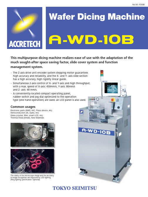
No.92-1035BThis multipurpose dicing machine realizes ease of use with the adaptation of themuch sought-after space saving factor, slide cover system and functionmanagement system.-The Z-axis drive unit encoder system stepping motor guaranteeshigh accuracy and reliability, and the X- and Y- axis slide sectionhas a high accuracy, high rigidity linear guide.-Simultaneous 2-axis control of X- and Y-axis and high throughput,with a max. speed of X-axis: 450mm/s, Y-axis: 80mm/sand Z- axis: 40 mm/s.-A conveniently-located compact operating panel,rubber switch and jog dial optimized to the operationtype (one hand operation) are used; an LCD panel is also used.Common usagesElectronic parts (SMD, HIC, Piezo device, etc)Semiconductors (Si, GaAs, etc)Glass (crystal, filter, small LCD, etc)Thermal Head (Small), New MaterialsThe clarity of the microscope image and the accuracyof image recognition are improved by LED lighting.(Ring lighting specification: Optional)A-WD-10B SPECIFICATIONSUser-friendly Operating Panel Operation DisplayMain OptionsNon-contact optical cutter setting unit Blade breakage detector 3” flange compatibilityY-scale positioning accuracy:2 µm/162 mm Cover interlock Ring lightingMiddle power spindle 3 color indication lamp Mist fan CE markingA-CS-100A (Spin Cleaner/Dryer)Function Management SystemRegistering frequently used functions and creating shortcuts improves operability.A-CS-100A (Optional)。
日本东京精密

东京精密株式会社公司简介东京精密株式会社是日本著名半导体制造设备之一,公司总部设在日本东京都三鹰市, 在美国,欧洲,新加坡,中国等地设有分公司,研发基地或生产厂等.We develop our businesses in two key areas: semiconductor manufacturing equipment and precision measuring systems. Our philosophy is to generate long-term growth through the creation of "WIN-WIN," or mutually beneficial, relationships, with all our stakeholders - customers, business partners, shareholders and employees.(公司网站原文)东京精密主要从事半导体加工设备及精密测量仪器制造及开发. 半导体加工设备有硅片加工用地倒角机、内圆切片机, 半导体加工前道工序用的光刻机(LEEPL)、CMP、晶片表面综合检查设备及测试封装用的探针台、划片机、硅片背面抛光机等.过去,东京精密简称“TSK”,在国内半导体行业享有盛誉。
现在东京精密采用了新的商标“ACCRETECH”,她是由英文成长ACCRETE和技术TECHNOLOGY的合成词,是融合公司”以WIN-WIN精神工作,创世界一流产品“经营理念的新标志。
参展产品:硅片材料的内圆切片机、硅片倒角机,光刻机,CMP,硅片表面检查系统,探针台背面减薄抛光机,划片机。
网址:http://www.accretech.jp/Semiconductor Manufacturing Equipment:Product listWafer Manufacturing SystemVariety of products line for wafer manufacturers including Wafer Slicing Machine and Wafer Edge Grinding Machine.Sliced Wafer Carbon Demounting and Cleaning Machine : C-RW-200/300Feature 1Automatic demounting of wafers from the slicing base, cleaning and storing into the cassette.Wafer Edge Grinding: W-GM-5200•Newly-developed grinding unit enhances the rotative precision of the spindle, and improves the surface roughness.•The non-contact measuring method achieves the stable alignment.•Performs the non-contact measuring of the pre-processed wafer thickness at multiple points, the diameter and notch depth of thepost-processed wafer.•The modular concept to make the optimum process line possible.•Low damage grinding method is available.Feature 1Machine specification ready for 300 mm and 200 mm wafer.Feature 2Visual system (optional) for measuring the chamfer width of periphery and notch.Wafer Edge Grinding: W-GM-4200•Newly-developed grinding unit enhances the rotative precision of the spindle, and improves the surface roughness.•The non-contact measuring method achieves the stable alignment.•Performs the non-contact measuring of the pre-processed wafer thickness at multiple points, the diameter and notch depth of thepost-processed wafer.•The modular concept to make the optimum process line possible.•Low damage grinding method is available.Feature 1Machine specification ready for 75 - 150 mm wafer or for 150 - 200 mm wafer. Feature 2Capable of various material processes, such as chemical compound semiconductor.Wafer Slicing Machine: S-LM-116GPrecise slicing machine for fragile materials such as glass, ceramics, ferrite. Feature 116"-size blade for easy handling, lifting and adjustment.Feature 2Open-structure loading unit for easy mounting of the workpiece.Feature 3Easy setting of slicing speed and wafer thickness with digital switch.Feature 4Strong frame, highly rigid table provides long-term stability in performance. Feature 5Easy coolant adjustment and dressing operation.Wafer Slicing Machine: A-WS-100SScribes wafer substrate with high precisionFeature 1Easy alignmentWith fine adjustment in horizontal and rotative directionsFeature 2Easy scribe settingWith the touch panel to set the index amount, number of times of scribing, etc. CMPCMPs remove unevenness on wafer surfaces that occur during the production process. Applications are growing due to the increase of layers in semiconductor devices and the growing variety of wiring materials. ChaMP: For 300mm WafersCombining the technological expertise built up by Accretech in precision measuring equipment and semiconductor manufacturing equipment, we now offer "the ChaMP Series", the CMP systems compatible with 300 mm wafers, with process performance required by design rules for 90 nm and 32 nm devices, and able to keep up with the most advanced volume-production fabs.Feature 1Air-float Head "Sylphide"•Reference polishing is made possible via an air cushion that provides uniform pressure distribution.•Wafer pressure is applied by an airbag independent of ring pressure, providing excellent low-pressure controllability and stability.•Zone control is available.Feature 2Edge Exclusion of 1 mm!Feature 3Wafer Pressure Controllability & RepeatabilityFeature 4Simple Maintenance for Polishing Heads - Ring Change Demounting (approximately 5 seconds)Slide the snap ring cover up with both handsSpread the snap ring with your thumb (the retaining ring drops off)Completely remove the retaining ringMounting (approximately 10 seconds)1. Grip the snap ring with both hands and push the retainer into thecarrier. Rotate it slightly to align the faces where the positioningframe slips into place.2. Attach the snap ring round the whole circumference and slide thecover down.ChaMP: For 150 or 200mm WafersFor 150 or 200mm WafersChaMP: Compact CMP SystemSmall footprintWafer Probing MachinesWafer probing machines perform electrical tests of each chip on a wafer, ensuring the quality of semiconductor devices.Wafer Probing Machines: UF3000EXNext-generation high-spec probing machine the world No.1 supplier presents Phenomenal levels of throughput have been made possible with the synergistic effects of high-speed wafer handling enabled by a new algorithm, and the high-speed and low-noise XY Stage enabled by a newly developed purpose-built drive unit for probes. The Z axis ensures world-class load capacity and high precision, and offers excellent contact via an optimal structural design that employs topology which reliably eliminates changes in flatness due to positioning.With advanced OTS latest positioning system technology and by colorizing wafer alignment imaging and equipping a light super magnification function, the UF3000EX has improved dramatically in terms of precision and operability. Wafer Probing Machines: UF3000EX-eAssimilating the up-to-date technologies such as originative OTS, QPU and TTG, this super high-spec system provides the testing system which meets your needs for the miniaturization of the next-generation devices and various testing environment.Feature 1OTS - the newest positioning technology (Optical Target Scope)OTS enables to measure the relative position of the cameras with absolute accuracy, which improved dramatically.Based on the ACCRETECH metrology technology, OTS enables theself-correlation of the alignment optical system.Feature 2QPU - super high-rigid chucking (Quad-Pod Unit)To effectively attain the accuracy in positioning, the high rigidity of every part is greatly important.The UF3000 uses the new technology of 4 axes driving mechanism (QPU) for Z-axis, enabling the high-rigid, stable probe contact.Feature 3Load-portTesting environment satisfying the users' needs is available by the common platform of 8-inch and 12-inch cassettes and the front allocation of the inspection tray. The machine is also ready for AMHS (Automated Material Handling System).Feature 4TTG (Touch To Go)Pursuing the easy operation, the UF3000 adopts the function to move to the position you touch on the map or image shown on the touch panel. Setting up is easy, and screen configuration is possible by the user definition.Wafer Probing Machine: UF2000Tokyo Seimitsu, now known as Accretech, has continued to lead the semiconductor industry as the world's number one manufacturer of wafer probing machines. The newly developed UF2000 high-precision 200mm wafer prober is designed for devices with decreasing pad pitches typified by LCD drivers and other such devices, and features enhanced functionality in all areas, while offering the same functions and operating ease as the previous model.Feature 1Achieves overall precision of ±1.5µm.Feature 2Adopts new processor, newly designed loader and image processing system with enhanced performance, dramatically boosting throughput.Wafer Probing Machine: UF200REvolving and Proliferating Wafer Probing Machine, UF SeriesBased on a flexible platform, the high accuracy and high rigidity, UF series is further evolved. Wafers are varying with the progress of line width shrinkage and assembly technology. This machine can be used for processing very thin wafers and can be used as a handler for the wafer level burn-in system.Feature 18-inch multipurpose machine.Wafer Probing Machine: UF190REvolving and Proliferating Wafer Probing Machine, UF SeriesBased on a flexible platform, the high accuracy and high rigidity, UF series is further evolved. Wafers are varying with the progress of line width shrinkage and assembly technology. This machine can be used for processing very thin wafers and can be used as a handler for the wafer level burn-in system.Feature 1High-performance, high-throughput, and excellent cost performance machine.Feature 2The UF190A features the same high-performance and excellent operability as the UF200 earned a reputation including the automatic needle alignment function and the color LCD touch panel.Wafer Probing Machine: FP200AEvolving and Proliferating Wafer Probing Machine, UF Series Based on a flexible platform, the high accuracy and high rigidity, UF series is further evolved. Wafers are varying with the progress of line width shrinkage and assembly technology. This machine can be used for processing very thin wafers and can be used as a handler for the wafer level burn-in system. Feature 1Frame transfer ready for the thinner wafer.Wafer Probing Machines Network: VEGANETThe operation status of the wafer probing machines can be centralizedly monitored to further improve the operation rateSystem monitorOperation rate controlProber status monitorData analysisWafer Probing Machines Network: LIGHTVEGAThe resource control will be centralized on the user hostWafer Probing Machines Network: GEM Network SystemWafer Probing Machines Network: VEGA PLANETDedicated terminals contributing to the efficiency enhancement of test areas Feature 1Device data compile terminalFeature 2Remote operation terminalFeature 3Logging data analysis terminalFeature 4Map viewerPolish GrindersPolish grinders simultaneously thin wafers while performing damage removal caused by the grinding process, and offer various applications for peripheral processes in the one system.Polish Grinder: PG3000/PG200PG3000PG200The product of a unique ACCRETECH innovation, this Polish Grinder combines the wafer thinness required for IC cards and three-dimensional mounting technology with damage removal functions in a single device.Feature 1Performs the processes of the rough grinding, fine grinding, polishing and cleaning wafers on the both sides in a single machine.Feature 2All the processes are completed without moving the wafer on the same chuck table.Feature 3The smallest footprint in the worldFeature 4Environmental - friendly - subsurface damage reduction without chemicals. Feature 5System configurationPolish Grinder: PG3000RM/PG200RMPG3000 RM : For 300mm WafersPG200 RM : For 200mm WafersACCRETECH also offers the "RM option", having the additional process of the tape removing for thinner wafer after the tape mounting, in addition to the standard process of PG300/200.Feature 1Optional RM moduleThe RM200/300 offers a single-unit solution supplementing PG200/300 processing with additional functionality to remove protective tape from thinner wafers and apply wafers to dicing frames.Feature 2Performs the processes of the rough grinding, fine grinding, polishing and cleaning wafers on the both sides in a single machine.Feature 3All the processes are completed without moving the wafer on the same chuck table.Feature 4The smallest footprint in the world.Feature 5Environmental - friendly - subsurface damage reduction without chemicals. Feature 6System configurationWafer Dicing MachinesWafer dicing machine cut wafers into individual semiconductor chips with blades. ACCRETECH Laser dicing machines use lasers instead of blades to dicewafers at high speed in a completely dry process.Wafer Dicing Machines:AD3000T/STokyo Seimitsu Wafer Dicing Machine realizes the remarkable “CoO (Cost of Owne rship)” by the world smallest footprint, high throughput, and high processing quality reinforced by the collaboration of theup-to-date technology.Wafer Dicing Machines:A-WD-200THigh throughput achieved by a new conceptThe A-WD-200T uses an opposing, twin spindle arrangement. Thisunique concept minimizes motion and delivers a massive boost inthroughput.Wafer Dicing Machines:A-WD-250SFully automated dicing machine for 8 inch wafer and large-sizedsubstratesWafer Dicing Machines: AD20TRevolutionary axis design orientation creates the smallest twin spindleDicing SawWafer Dicing Machines:A-WD-10BThis multipurpose dicing machine realizes ease of use with theadaptation of the much sought-after space saving factor, slide coversystem and functionmanagement system.Wafer Dicing Machines:PS280Now, with two independent stages, cutting and positioning canproceed in parallel. The result - a maximum dicing speed up to twicethat previously possible!New connected handlers, shorten coordination time - bringingincreased operation efficiency and substantial savings in processingtime.Automatic Cleaning System:A-CS-100AStand-alone wafer cleaning unit, A-CS-100A will provide best solution for cleaning and drying the wafer such as sawn with semi-automaticdicing saws.High-pressure water spray up to 10 MPa driven by horizontal swinging arm will achieve excellent cleaning quality.Wafer Dicing Machines:ML300High performance laser dicing machine for 300 mm wafers with SDE.Wafer Dicing Machines:ML200We have developed a dicing machine equipped with stealth dicingtechnology (developed by Hamamatsu Photonics) as a stealth dicingengine, exhibiting excellent performance.Precision ACCRETECH BladeWith the diamond, the world-hardest substance, super-abrasive grit,we offer the cutting blade and solution that are high quality and costcutting.•Precision ACCRETECH BladeProduct listMeasuring Systems:Product list"No measurement,no manufacturing" - ACCRETECH supplys the best from Multi-perpose measuring to In-line measuring.Automatic Measuring SystemsMachine control gauges control processing machines based on data taken before, during and after operation. This indispensable system is used to prevent defects and boost accuracy in manufacture, thereby raising productivity. We also produce air micrometers, electric micrometers and high-precision sensors.•Machine Control Gauges•Various Sensors and Electric / Air Micrometers•High Precisions Digital Measurement Instrument•Laser Interferometer / Built-in Measuring Instruments•Automatic Measuring SystemsIndustrial Measuring SystemsWe manufacture a variety of high-precision industrial measuring systems, including: 3D Coordinate Measuring Machines, Surface Texture and Contour Measuring Instruments and Cylindrical Form Measuring Instruments.•3D Coordinate Measuring Machines•Surface Texture and Contour Measuring Instruments•Roundness and Cylindrical Profile Measuring Instruments。
基于表面粗糙度参数的管道当量粗糙度快速评测

基于表面粗糙度参数的管道当量粗糙度快速评测郭永鑫;杨开林;郭新蕾;李甲振;付辉【摘要】管道水力摩阻系数的精确取值是输水工程水力设计的重要前提,当量粗糙度k是计算水力摩阻系数的基础参数,然而传统的水力学试验方法检测k值需耗费较多的人、财、物、时.研究首先对3种不同粗糙度内衬的球墨铸铁管进行水力学性能的试验检测,基于不确定度理论给出合理的k值.在此基础上,采用触针式表面粗糙度仪对管道内壁的表面粗糙度参数进行检测,将检测结果与k值进行比较,结合国外已有试验数据,分析给出工程中管道k值的快速评测方法:当粗糙度轮廓的算术平均偏差Ra≤10 μm或粗糙度轮廓的最大高度Rz≤50 μm时,取样长度为lr=2.5 mm,采用中线制评定所得的Rz-≈k,可使用Rz值代表k值对管道的水力性能进行评价.研究成果也可用于生产中管道内涂层加工质量的控制和提高.%The accurate friction factor of pipeline is an important prerequisite during the hydraulic design process of water conveyance project.The equivalent sand-grain roughness is a key parameter to calculate the pipeline frictionfactor.However,it takes lots of manpower,material,financial resources and time to measure the equivalent sand-grain roughness by the traditional hydraulic test method.In this study,the hydraulic performances of 3 kinds of ductile iron pipes with different coatings were tested,and the equivalent sand-grain roughness values were obtained based on the measure uncertainty analysis,respectively.Then,the inner wall surface roughness parameters of 3 kinds of pipes were detected by the E-35B portable surface roughness tester profilometer.By the comparison of the surface roughness parameters and the equivalent sand-grain roughness k,and thereanalysis of others researcher's data,a quick evaluation method of pipe equivalent sand-grain roughness based on the surface roughness parameters was given:when the arithmetical mean deviation of roughness profile Ra≤ l0μm or the maximum height of roughness profileRz≤50μm,the sampling length of roughness profile lr set to 2.5mm,then Rz-≈k.So,the equivalent sand-grain roughness k in the Colebrook-White formula was replaced with Rz,and the friction factor can be calculated.The research results can also be used to control and improve the coating quality of pipeline.【期刊名称】《水利学报》【年(卷),期】2018(049)002【总页数】8页(P178-185)【关键词】管道;水力摩阻系数;测量不确定度;表面粗糙度参数;当量粗糙度【作者】郭永鑫;杨开林;郭新蕾;李甲振;付辉【作者单位】中国水利水电科学研究院流域水循环模拟与调控国家重点试验室,北京100038;中国水利水电科学研究院流域水循环模拟与调控国家重点试验室,北京100038;中国水利水电科学研究院流域水循环模拟与调控国家重点试验室,北京100038;中国水利水电科学研究院流域水循环模拟与调控国家重点试验室,北京100038;中国水利水电科学研究院流域水循环模拟与调控国家重点试验室,北京100038【正文语种】中文【中图分类】TV1341 研究背景管道水力摩阻系数是流体输送工程设计的重要技术参数之一,在一定的压力和输送流量下,其取值的结果直接影响水力计算成果的精度,进而影响到工程的总体布局、设计规模、投资乃至运行费用。
株式会社东京精密(日本)企业信用报告-天眼查

截止 2018 年 11 月 15 日,根据国内相关网站检索及天眼查数据库分析,未查询到相关信息。不排除因信 息公开来源尚未公开、公开形式存在差异等情况导致的信息与客观事实不完全一致的情形。仅供客户参 考。
5
4.5 竞品信息
截止 2018 年 11 月 15 日,根据国内相关网站检索及天眼查数据库分析,未查询到相关信息。不排除因信 息公开来源尚未公开、公开形式存在差异等情况导致的信息与客观事实不完全一致的情形。仅供客户参 考。
5.3 法律诉讼
截止 2018 年 11 月 15 日,根据国内相关网站检索及天眼查数据库分析,未查询到相关信息。不排除因信 息公开来源尚未公开、公开形式存在差异等情况导致的信息与客观事实不完全一致的情形。仅供客户参 考。
6
5.4 法院公告
截止 2018 年 11 月 15 日,根据国内相关网站检索及天眼查数据库分析,未查询到相关信息。不排除因信 息公开来源尚未公开、公开形式存在差异等情况导致的信息与客观事实不完全一致的情形。仅供客户参 考。
/
注册地址:
/
营业期限:
/至/
经营范围:
/
登记机关:
/
核准日期:
/
1.2 分支机构
截止 2018 年 11 月 15 日,根据国内相关网站检索及天眼查数据库分析,未查询到相关信息。不排除因信 息公开来源尚未公开、公开形式存在差异等情况导致的信息与客观事实不完全一致的情形。仅供客户参
3
考。
1.3 变更记录
截止 2018 年 11 月 15 日,根据国内相关网站检索及天眼查数据库分析,未查询到相关信息。不排除因信 息公开来源尚未公开、公开形式存在差异等情况导致的信息与客观事实不完全一致的情形。仅供客户参 考。
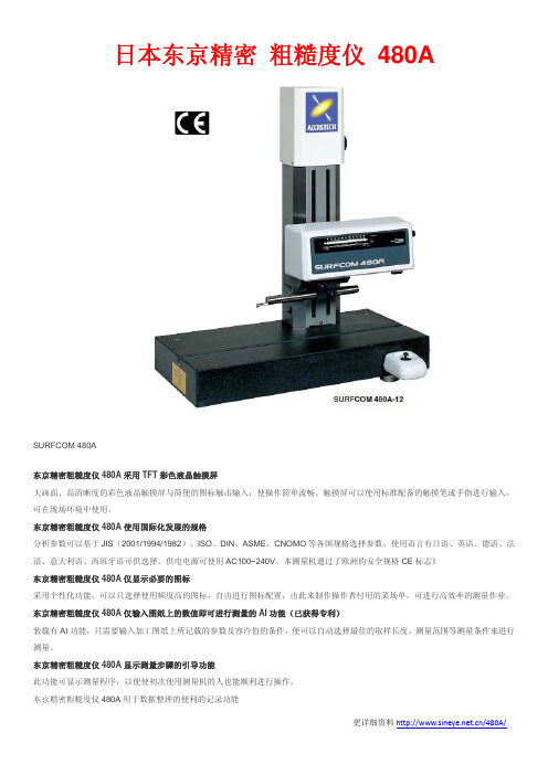
东京精密粗糙度仪
倍率
纵倍率(Z 轴) 50、100、200、500、1K、2K、5K、10K、100K、200K*、500K*倍、自动
横倍(X 轴)
1、2、5、10、20、50、100、200、500、1K、2K、自动
滤波器的种类
标准型滤波器 2RC、相位补偿型滤波器 2RC、相位补偿型滤波器(高斯滤波器)
测量速度
tlllrpcrskrkurkrpkrvkmr1mr2voktprmrtp2rmr2rdcavhhmaxhminareancrxrrxarnrcpmsrsar评价曲线剖面曲线粗糙度曲线滤波波纹度曲线滤波中心线波纹度曲线滚动圆波纹度曲线滚动圆中心线波纹度曲线din4776特殊曲线粗糙度中心曲线motif波纹度中心曲线motif包络波纹度曲线表面特性图表负荷曲线功率谱曲线图振幅分布曲线倾斜补偿方式直线补偿r面补偿前半补偿后半补偿两端补偿花键补偿直线r两端补偿可以在任意范围内倍率纵倍率z1251020501002005001k2k自动滤波器的种类标准型滤波器2rc相位补偿型滤波器2rc相位补偿型滤波器高斯滤波器测量速度00300601503006015传感器前端半径2mm材质为金刚石测量力为075mn先进的功能测量ai装载有测量ai功能即使初学者也可容易掌握段差分析功能最适于测量半导体零部件的膜厚及面积pc输出文本文件将数据传送至电脑标准配件标准片emcs24b记录纸echs21a触摸笔emas54a操作说明书各要素电源ac100240v105060hz90va设置尺寸1000w800d750hmm质量105kg
SURFCOM 480A
型号
测量范围
X 轴(横向) Y 轴(纵向)
100mm 800mm(测量范围/分辩率:800mm/10nm、80mm/1nm、8mm/0.1nm)
引导主流 创造“双赢”——访日本东京精密董事长兼CEO大坪英夫先生
引导主流创造“双赢”——访日本东京精密董事长兼CEO大
坪英夫先生
郑文灏
【期刊名称】《中国集成电路》
【年(卷),期】2002(000)005
【摘要】在2002北京微电子国际研讨会期间本刊记者有莘在北京天鸿科园大酒店采访了与会的日本东京精密董事长兼CEO大坪英夫(HIDEO OHTSUBO)先生。
大坪先生首先向我们介绍了他们公司的概况:东京精密创建于1949年,主要产品是精密测量仪器和半导体制造设备,我们研究与开发的战略目标是使我们的产品居"世界第一";我们的营销方针是"双赢(Win-Win)"政策,
【总页数】2页(P8-9)
【作者】郑文灏
【作者单位】
【正文语种】中文
【中图分类】F416.63
【相关文献】
1.风动"艾岑"——访AERZEN集团董事长兼CEO HELLER先生 [J], 朱宇
2.ACC集团:中国是发展重点——访ACC集团董事长兼CEO Valter Taranzano 先生 [J], 黄敏
3.百度:创造200个百万富翁--访百度董事长兼CEO李彦宏 [J],
4.为用户和投资人创造长期价值——访广州小鹏汽车科技有限公司董事长兼CEO 何小鹏 [J], 韦敏
5.品质品牌“品”优德——访优德精密工业(昆山)有限公司董事长兼总经理曾正雄先生及美国DADCO公司总裁Michael C.Diebolt先生 [J], 瞿华明
因版权原因,仅展示原文概要,查看原文内容请购买。
曲轴车-车梳加工工艺分析及切削模拟实验研究
曲轴车-车梳加工工艺分析及切削模拟实验研究张朝辉;何云;刘晋;徐忠意【摘要】Turn-turn chasing process is widely used in the rough and semi-finish machining of crankshafts of modern vehicles. In this paper, takingthe process as the research subject, the turn-turn chasing process and cutting characteristics was analyzed. Based on an experimental platform which includes a remolded CNC machine applied to turn-turn chasing process and a newly manufactured tool system, the simulated turn-turn chasing cutting experiment was conducted. Machining quality was evaluated in three aspects, the shaft collar roundness, surface roughness and shaft collar side wall surface roughness. Experimental data and the results of the study have a certain reference value for the improvementand application of domestic crankshaft processing.%车-车梳工艺是现今汽车发动机曲轴主轴颈的粗、半精加工中广泛应用的切削工艺.以车-车梳工艺为研究对象,分析了车梳复合切削特性以及车-车梳加工工艺流程.并以一套自主改造的车-车梳数控机床和配套的刀具系统为实验平台,进行了车-车梳切削模拟实验,从轴颈圆度、表面粗糙度及轴颈侧壁表面粗糙度三个方面对加工质量进行了评估.实验数据及研究结果对国内曲轴加工工艺的改进和应用有一定的参考价值.【期刊名称】《柴油机设计与制造》【年(卷),期】2015(021)004【总页数】6页(P43-48)【关键词】曲轴;车-车梳;工艺分析【作者】张朝辉;何云;刘晋;徐忠意【作者单位】华东理工大学机械与动力工程学院、机械工程系,上海 200237;华东理工大学机械与动力工程学院、机械工程系,上海 200237;华东理工大学机械与动力工程学院、机械工程系,上海 200237;华东理工大学机械与动力工程学院、机械工程系,上海 200237【正文语种】中文曲轴是汽车发动机的重要部件,其制造质量好坏直接影响了汽车的性能。
- 1、下载文档前请自行甄别文档内容的完整性,平台不提供额外的编辑、内容补充、找答案等附加服务。
- 2、"仅部分预览"的文档,不可在线预览部分如存在完整性等问题,可反馈申请退款(可完整预览的文档不适用该条件!)。
- 3、如文档侵犯您的权益,请联系客服反馈,我们会尽快为您处理(人工客服工作时间:9:00-18:30)。
东京精密株式会社公司简介东京精密株式会社是日本著名半导体制造设备之一,公司总部设在日本东京都三鹰市, 在美国,欧洲,新加坡,中国等地设有分公司,研发基地或生产厂等.We develop our businesses in two key areas: semiconductor manufacturing equipment and precision measuring systems. Our philosophy is to generate long-term growth through the creation of "WIN-WIN," or mutually beneficial, relationships, with all our stakeholders - customers, business partners, shareholders and employees.(公司网站原文)东京精密主要从事半导体加工设备及精密测量仪器制造及开发. 半导体加工设备有硅片加工用地倒角机、内圆切片机, 半导体加工前道工序用的光刻机(LEEPL)、CMP、晶片表面综合检查设备及测试封装用的探针台、划片机、硅片背面抛光机等.过去,东京精密简称“TSK”,在国内半导体行业享有盛誉。
现在东京精密采用了新的商标“ACCRETECH”,她是由英文成长ACCRETE和技术TECHNOLOGY的合成词,是融合公司”以WIN-WIN精神工作,创世界一流产品“经营理念的新标志。
参展产品:硅片材料的内圆切片机、硅片倒角机,光刻机,CMP,硅片表面检查系统,探针台背面减薄抛光机,划片机。
网址:http://www.accretech.jp/Semiconductor Manufacturing Equipment:Product listWafer Manufacturing SystemVariety of products line for wafer manufacturers including Wafer Slicing Machine and Wafer Edge Grinding Machine.Sliced Wafer Carbon Demounting and Cleaning Machine : C-RW-200/300Feature 1Automatic demounting of wafers from the slicing base, cleaning and storing into the cassette.Wafer Edge Grinding: W-GM-5200•Newly-developed grinding unit enhances the rotative precision of the spindle, and improves the surface roughness.•The non-contact measuring method achieves the stable alignment.•Performs the non-contact measuring of the pre-processed wafer thickness at multiple points, the diameter and notch depth of thepost-processed wafer.•The modular concept to make the optimum process line possible.•Low damage grinding method is available.Feature 1Machine specification ready for 300 mm and 200 mm wafer.Feature 2Visual system (optional) for measuring the chamfer width of periphery and notch.Wafer Edge Grinding: W-GM-4200•Newly-developed grinding unit enhances the rotative precision of the spindle, and improves the surface roughness.•The non-contact measuring method achieves the stable alignment.•Performs the non-contact measuring of the pre-processed wafer thickness at multiple points, the diameter and notch depth of thepost-processed wafer.•The modular concept to make the optimum process line possible.•Low damage grinding method is available.Feature 1Machine specification ready for 75 - 150 mm wafer or for 150 - 200 mm wafer. Feature 2Capable of various material processes, such as chemical compound semiconductor.Wafer Slicing Machine: S-LM-116GPrecise slicing machine for fragile materials such as glass, ceramics, ferrite. Feature 116"-size blade for easy handling, lifting and adjustment.Feature 2Open-structure loading unit for easy mounting of the workpiece.Feature 3Easy setting of slicing speed and wafer thickness with digital switch.Feature 4Strong frame, highly rigid table provides long-term stability in performance. Feature 5Easy coolant adjustment and dressing operation.Wafer Slicing Machine: A-WS-100SScribes wafer substrate with high precisionFeature 1Easy alignmentWith fine adjustment in horizontal and rotative directionsFeature 2Easy scribe settingWith the touch panel to set the index amount, number of times of scribing, etc. CMPCMPs remove unevenness on wafer surfaces that occur during the production process. Applications are growing due to the increase of layers in semiconductor devices and the growing variety of wiring materials. ChaMP: For 300mm WafersCombining the technological expertise built up by Accretech in precision measuring equipment and semiconductor manufacturing equipment, we now offer "the ChaMP Series", the CMP systems compatible with 300 mm wafers, with process performance required by design rules for 90 nm and 32 nm devices, and able to keep up with the most advanced volume-production fabs.Feature 1Air-float Head "Sylphide"•Reference polishing is made possible via an air cushion that provides uniform pressure distribution.•Wafer pressure is applied by an airbag independent of ring pressure, providing excellent low-pressure controllability and stability.•Zone control is available.Feature 2Edge Exclusion of 1 mm!Feature 3Wafer Pressure Controllability & RepeatabilityFeature 4Simple Maintenance for Polishing Heads - Ring Change Demounting (approximately 5 seconds)Slide the snap ring cover up with both handsSpread the snap ring with your thumb (the retaining ring drops off)Completely remove the retaining ringMounting (approximately 10 seconds)1. Grip the snap ring with both hands and push the retainer into thecarrier. Rotate it slightly to align the faces where the positioningframe slips into place.2. Attach the snap ring round the whole circumference and slide thecover down.ChaMP: For 150 or 200mm WafersFor 150 or 200mm WafersChaMP: Compact CMP SystemSmall footprintWafer Probing MachinesWafer probing machines perform electrical tests of each chip on a wafer, ensuring the quality of semiconductor devices.Wafer Probing Machines: UF3000EXNext-generation high-spec probing machine the world No.1 supplier presents Phenomenal levels of throughput have been made possible with the synergistic effects of high-speed wafer handling enabled by a new algorithm, and the high-speed and low-noise XY Stage enabled by a newly developed purpose-built drive unit for probes. The Z axis ensures world-class load capacity and high precision, and offers excellent contact via an optimal structural design that employs topology which reliably eliminates changes in flatness due to positioning.With advanced OTS latest positioning system technology and by colorizing wafer alignment imaging and equipping a light super magnification function, the UF3000EX has improved dramatically in terms of precision and operability. Wafer Probing Machines: UF3000EX-eAssimilating the up-to-date technologies such as originative OTS, QPU and TTG, this super high-spec system provides the testing system which meets your needs for the miniaturization of the next-generation devices and various testing environment.Feature 1OTS - the newest positioning technology (Optical Target Scope)OTS enables to measure the relative position of the cameras with absolute accuracy, which improved dramatically.Based on the ACCRETECH metrology technology, OTS enables theself-correlation of the alignment optical system.Feature 2QPU - super high-rigid chucking (Quad-Pod Unit)To effectively attain the accuracy in positioning, the high rigidity of every part is greatly important.The UF3000 uses the new technology of 4 axes driving mechanism (QPU) for Z-axis, enabling the high-rigid, stable probe contact.Feature 3Load-portTesting environment satisfying the users' needs is available by the common platform of 8-inch and 12-inch cassettes and the front allocation of the inspection tray. The machine is also ready for AMHS (Automated Material Handling System).Feature 4TTG (Touch To Go)Pursuing the easy operation, the UF3000 adopts the function to move to the position you touch on the map or image shown on the touch panel. Setting up is easy, and screen configuration is possible by the user definition.Wafer Probing Machine: UF2000Tokyo Seimitsu, now known as Accretech, has continued to lead the semiconductor industry as the world's number one manufacturer of wafer probing machines. The newly developed UF2000 high-precision 200mm wafer prober is designed for devices with decreasing pad pitches typified by LCD drivers and other such devices, and features enhanced functionality in all areas, while offering the same functions and operating ease as the previous model.Feature 1Achieves overall precision of ±1.5µm.Feature 2Adopts new processor, newly designed loader and image processing system with enhanced performance, dramatically boosting throughput.Wafer Probing Machine: UF200REvolving and Proliferating Wafer Probing Machine, UF SeriesBased on a flexible platform, the high accuracy and high rigidity, UF series is further evolved. Wafers are varying with the progress of line width shrinkage and assembly technology. This machine can be used for processing very thin wafers and can be used as a handler for the wafer level burn-in system.Feature 18-inch multipurpose machine.Wafer Probing Machine: UF190REvolving and Proliferating Wafer Probing Machine, UF SeriesBased on a flexible platform, the high accuracy and high rigidity, UF series is further evolved. Wafers are varying with the progress of line width shrinkage and assembly technology. This machine can be used for processing very thin wafers and can be used as a handler for the wafer level burn-in system.Feature 1High-performance, high-throughput, and excellent cost performance machine.Feature 2The UF190A features the same high-performance and excellent operability as the UF200 earned a reputation including the automatic needle alignment function and the color LCD touch panel.Wafer Probing Machine: FP200AEvolving and Proliferating Wafer Probing Machine, UF Series Based on a flexible platform, the high accuracy and high rigidity, UF series is further evolved. Wafers are varying with the progress of line width shrinkage and assembly technology. This machine can be used for processing very thin wafers and can be used as a handler for the wafer level burn-in system. Feature 1Frame transfer ready for the thinner wafer.Wafer Probing Machines Network: VEGANETThe operation status of the wafer probing machines can be centralizedly monitored to further improve the operation rateSystem monitorOperation rate controlProber status monitorData analysisWafer Probing Machines Network: LIGHTVEGAThe resource control will be centralized on the user hostWafer Probing Machines Network: GEM Network SystemWafer Probing Machines Network: VEGA PLANETDedicated terminals contributing to the efficiency enhancement of test areas Feature 1Device data compile terminalFeature 2Remote operation terminalFeature 3Logging data analysis terminalFeature 4Map viewerPolish GrindersPolish grinders simultaneously thin wafers while performing damage removal caused by the grinding process, and offer various applications for peripheral processes in the one system.Polish Grinder: PG3000/PG200PG3000PG200The product of a unique ACCRETECH innovation, this Polish Grinder combines the wafer thinness required for IC cards and three-dimensional mounting technology with damage removal functions in a single device.Feature 1Performs the processes of the rough grinding, fine grinding, polishing and cleaning wafers on the both sides in a single machine.Feature 2All the processes are completed without moving the wafer on the same chuck table.Feature 3The smallest footprint in the worldFeature 4Environmental - friendly - subsurface damage reduction without chemicals. Feature 5System configurationPolish Grinder: PG3000RM/PG200RMPG3000 RM : For 300mm WafersPG200 RM : For 200mm WafersACCRETECH also offers the "RM option", having the additional process of the tape removing for thinner wafer after the tape mounting, in addition to the standard process of PG300/200.Feature 1Optional RM moduleThe RM200/300 offers a single-unit solution supplementing PG200/300 processing with additional functionality to remove protective tape from thinner wafers and apply wafers to dicing frames.Feature 2Performs the processes of the rough grinding, fine grinding, polishing and cleaning wafers on the both sides in a single machine.Feature 3All the processes are completed without moving the wafer on the same chuck table.Feature 4The smallest footprint in the world.Feature 5Environmental - friendly - subsurface damage reduction without chemicals. Feature 6System configurationWafer Dicing MachinesWafer dicing machine cut wafers into individual semiconductor chips with blades. ACCRETECH Laser dicing machines use lasers instead of blades to dicewafers at high speed in a completely dry process.Wafer Dicing Machines:AD3000T/STokyo Seimitsu Wafer Dicing Machine realizes the remarkable “CoO (Cost of Owne rship)” by the world smallest footprint, high throughput, and high processing quality reinforced by the collaboration of theup-to-date technology.Wafer Dicing Machines:A-WD-200THigh throughput achieved by a new conceptThe A-WD-200T uses an opposing, twin spindle arrangement. Thisunique concept minimizes motion and delivers a massive boost inthroughput.Wafer Dicing Machines:A-WD-250SFully automated dicing machine for 8 inch wafer and large-sizedsubstratesWafer Dicing Machines: AD20TRevolutionary axis design orientation creates the smallest twin spindleDicing SawWafer Dicing Machines:A-WD-10BThis multipurpose dicing machine realizes ease of use with theadaptation of the much sought-after space saving factor, slide coversystem and functionmanagement system.Wafer Dicing Machines:PS280Now, with two independent stages, cutting and positioning canproceed in parallel. The result - a maximum dicing speed up to twicethat previously possible!New connected handlers, shorten coordination time - bringingincreased operation efficiency and substantial savings in processingtime.Automatic Cleaning System:A-CS-100AStand-alone wafer cleaning unit, A-CS-100A will provide best solution for cleaning and drying the wafer such as sawn with semi-automaticdicing saws.High-pressure water spray up to 10 MPa driven by horizontal swinging arm will achieve excellent cleaning quality.Wafer Dicing Machines:ML300High performance laser dicing machine for 300 mm wafers with SDE.Wafer Dicing Machines:ML200We have developed a dicing machine equipped with stealth dicingtechnology (developed by Hamamatsu Photonics) as a stealth dicingengine, exhibiting excellent performance.Precision ACCRETECH BladeWith the diamond, the world-hardest substance, super-abrasive grit,we offer the cutting blade and solution that are high quality and costcutting.•Precision ACCRETECH BladeProduct listMeasuring Systems:Product list"No measurement,no manufacturing" - ACCRETECH supplys the best from Multi-perpose measuring to In-line measuring.Automatic Measuring SystemsMachine control gauges control processing machines based on data taken before, during and after operation. This indispensable system is used to prevent defects and boost accuracy in manufacture, thereby raising productivity. We also produce air micrometers, electric micrometers and high-precision sensors.•Machine Control Gauges•Various Sensors and Electric / Air Micrometers•High Precisions Digital Measurement Instrument•Laser Interferometer / Built-in Measuring Instruments•Automatic Measuring SystemsIndustrial Measuring SystemsWe manufacture a variety of high-precision industrial measuring systems, including: 3D Coordinate Measuring Machines, Surface Texture and Contour Measuring Instruments and Cylindrical Form Measuring Instruments.•3D Coordinate Measuring Machines•Surface Texture and Contour Measuring Instruments•Roundness and Cylindrical Profile Measuring Instruments。