印刷电路板设计大全 Complete PCB Design Using OrCad Capture and Layout_Part5
印刷电路板PCB设计

03
02
3.5.4手动布线
将光标定位在排针Y1较低的焊盘(选中焊盘后,焊盘周围有一个小框围住)。左击鼠标或按Enter按钮,以确定线的起点。
04
检查文档工作区底部的层标签。如果Top Layer标签是激活的,按数字键盘上的“*”键,在不退出走线模式的情况下切换到底层。“*”键可用在信号层之间切换。
首先设计者要找到一个新的封装。单击Libraries面板,从库列表中选择Miscellaneous Deivices.IntLib[Footprint View],设计者要的是一个小一些的radial类型的封装,因此在过滤器栏键入rad,单击封装名就会看见与这名字相联系的封装,其中封装RAD-0.1就是设计者需要的,如图3-25所示。
02
将光标移向电阻R1底下的焊盘。注意:线段是如何跟随光标路径来在检查模式中显示的。状态栏显示的检查模式表明它们还没被放置。如果设计者沿光标路径拉回,未连接线路也会随之缩回。在这里,设计者有两种走线的选择。
Ctrl十左击鼠标,使用Auto-Complete功能,并立即完成布线(此技术可以直接使用在焊盘或连接线上)。起始和终止焊盘必须在相同的层内布线才有效,同时还要求板上的任何的障碍不会妨碍Auto-Complete的工作。对较大的板,Auto-Complete路径可能并不总是有效的,这是因为走线路径是一段接一段地绘制的,而从起始焊盘到终止焊盘的完整绘制有可能根本无法完成。
图3-21 修改线的宽度
(6)用以上的方法,在Design Rules面板单击名为Width_2的规则以修改其范围和约束。在名称栏键入GND;在Where The First Object Matches栏选择单选按钮Net,在选择框内单击向下的箭头,选择GND;将Min Width、Preferred Width和 Max Width宽度改为25mil。 注意导线的宽带由设计者自己决定,主要取决于设计者PCB板的大小与元器件的疏密。 (7)最后,单击最初的板子范围宽度规则名Width,将Min Width、Preferred Width和 Max Width宽度栏均设为12mil。 (8)单击图3-18的 按钮,弹出图3-22所示的优先级对话框,优先级(Priority)列的数字越小,优先级越高。可以按“Decrease Priority”按钮减少选中对象的优先级,按“Increase Priority”按钮增加选中对象的优先级,图3-18所示的GND的优先级最高,Width的优先级最低,单击Close按钮,关闭Edit Rule Priorities对话框,单击OK按钮,关闭PCB Rules and Constraints Editor 对话框。
第14讲印刷电路板设计
第14讲印刷电路板设计
一、印刷电路板的概述
印刷电路板(PCB)是将电子元件和电路相连的基础元素。
它是用于
连接组件的基本设计对象,可以容纳所有装配好的电子元件,并将它们连
接起来,形成功能复杂的电子电路。
印刷电路板(PCB)有很多种形式,主要有玻璃纤维基板、铜基板、
铝基板、陶瓷基板和碳纤维基板等几种基板。
它们主要有4个阶段:印刷
电路板设计、制板、装配和测试。
1、板材设计
印刷电路板(PCB)设计首先,必须选择板材,主要有玻璃纤维基板、铜基板、铝基板、陶瓷基板和碳纤维基板等几种。
选择板材根据客户的需
要和应用,主要考虑的是尺寸、厚度、薄板料的材质等,以及电气性能和
力学性能。
2、图案设计
印刷电路板(PCB)的设计必须结合印刷厂的设备水平及工艺要求,
达到厂家的要求。
图案设计是印刷电路板设计的关键,它要求成形制作过
程要尽可能简单,通过设计完成电路的网络。
常用的图案设计软件有Cadence Allegro、Altium Designer、PADS、KiCad、Eagle等,这些软件具有共同的基本功能,可以实现电路设计、
布线设计和封装设计的基本任务。
印刷电路板设计步骤
印刷电路板设计步骤好的,以下是印刷电路板(PCB)设计步骤:一、规划阶段首先呢,在设计印刷电路板之前,得有个整体的规划。
这就好比盖房子之前得有个设计图一样。
你得明确这个PCB板是干啥用的,有哪些元件得放在上面。
记住了,这个动作很重要哦。
比如说我以前做一个小的音频放大电路的PCB板,开始就没规划好,结果后面元件摆不下,又重新规划,浪费了好多时间。
1. 确定电路功能和要求- 把电路图先画出来,在纸上或者用电路设计软件(像Eagle或者Altium Designer)简单画个草图,把所有的元件都列出来。
这一步就像是厨师做菜前先把要用的食材都准备好放在面前。
这步我试过好多次,每次都要认真核对元件的参数、型号这些。
2. 确定PCB板的尺寸和形状- 要考虑这个PCB板是要装在一个特定的外壳里呢,还是可以自由设定尺寸。
要是装在现有外壳里,就得按照外壳的尺寸来,而且还得考虑端口、按钮这些的位置。
比如我以前做个小玩意要放在一个塑料盒子里,结果忘了留够位置给充电接口,真的很头疼。
所以这里一定要小心。
二、元件布局1. 初步布局- 把有特殊位置要求的元件先摆上去。
比如说,一些接口元件最好放在PCB板的边缘,方便接线。
就像家里的插座,都安装在墙边方便插电器一样。
这一步我之前就做错过,把接口放在中间了,后面发现接线很麻烦。
- 然后按照信号的流向,把主要的功能模块分开布局。
像处理信号的芯片放一块,功率放大的元件放另一块等。
在摆放的时候啊,要考虑元件之间的电磁兼容性(EMC)。
比如,模拟电路部分和数字电路部分最好隔远点,避免互相干扰。
对了这里可以用接地线来隔着不同的部分,这是个小窍门。
2. 优化布局- 检查元件之间的间距是否合适。
元件不能放得太挤,要预留足够的空间给焊接和返修。
我见过有人把元件挤得死死的,到时候焊接的时候烙铁都放不进去。
小元件比如贴片电容、电阻周围至少要留个几毫米的空间。
还有,要检查一下元件的引脚是否容易连线。
印制电路板(PCB板)设计
PCB设计一、 过孔:板厚和过孔比最好应大于3:1。
二、 焊盘尺寸:非过孔最小焊盘尺寸:D-d=1.0mm过孔最小焊盘尺寸:D-d=0.5mm过孔:D/d=1.5~2其中:D为焊盘直径,d为孔直径。
三、 测试方面的考虑:测试点可以考虑用方形来取代一般的圆形,以增加接触的可靠性,如果精度不是问题,也可以考虑用六或八边形的测试点,以便与辨认区别。
四、 布线:1、输入端与输出端的边线应避免相邻平行,以免产生反射干扰,必要时应加地线隔离,两相邻层的布线需互相垂直,平行容易产生寄生耦合。
2、众所周知的去噪方法是在电源、地线之间加上去耦电容,尽量加宽电源、地线宽度,最好是地线比电源线宽,它们的关系是:地线宽>电源线宽>信号线宽,通常信号线宽为0.2~0.3mm,最精细宽度可达0.05~0.07mm,电源线为1.2~2.5mm。
3、大面积导体中连接引脚的处理:在大面积的接地电中,兼顾电气性能与工艺需要,做成十字花焊盘,称之为热隔离,俗称热焊盘。
4、对于高频信号线最好用地线屏蔽。
多层板走线要求相邻两层印制板的线条应尽量相互垂直,或走斜线、曲线;大面积的电源层和大面积的地线层要相邻,实际上在电源和地之间形成了一个电容,能够起到滤波作用。
五、 焊盘设计控制(SMT):1、焊盘长度:焊盘可靠性主要取决与长度而不是宽度,一般长取0.5mm。
2、焊盘宽度:对于0805以上的阻容元件,或引脚脚间距在1.27mm以上的SO、SOJ等IC芯片,焊盘宽度一般是在元器件引脚宽度的基础上加一个数值,数值的范围在0.1~0.25mm之间;而对于0.65mm(包括0.65mm)脚间距以下的IC芯片,焊盘宽度应等于引脚的宽度;对于细间距的QFP,有的时候焊盘宽度相对于引脚来说还要适当减小。
3、过孔的处理:过孔与焊盘边缘之间的距离大于1mm。
六、 PCB生产工艺对设计的要求:1、单面板实验表明,当铜箔厚度为50um,导线宽度为1~1.5mm,通过2A电流时,温升很小。
二十2印刷电路板设计

注意:在有相应网络标号的场合只能使用交互式铜膜走线模式,否则DRC会将走线反 色表示错误。在没有网络的场合,两种走线模式都可以使用。
图5中的各个参数的具体含意如下: ★ Hole Size用于设置焊盘的通孔孔径大小。 ★ Rotation用于设置焊盘的起始角度。 ★ Location X(Y)分别用于设置焊盘中心在印刷电路板上的X坐标和Y坐标。 ★ Size and Shape选项区域内有三个选择项,具体含义如下: ★ Simple选中后使得焊盘在PCB板各层的X轴方向的大小、Y轴方向的大小和形状 都是相同的。其中X轴方向的大小、Y轴方向的大小是通过文本框设置的,而形状是 通过下拉列表框来选择的,在下拉框中一共有三种外形可供选择:Round(圆形)、 Rectangle(矩形)和Octagonal(八角形)。 ★ Top-Middle-Bottom选中后可以分别在不同板层上设置焊盘的大小。 ★ Full Stack选中后X-Size、Y-Size文本框和Shape下拉框会隐藏,而 Edit Full Pad Layer Definition按钮会反色突出,点击这一个按钮就会形象的看到 各层焊盘的设置情况。
二、创建PCB文件:
与原理图设计相同的是在进行印刷线路板设计之前必 须先创建一个PCB文件,而一般创建PCB文件有两种方 法:一是使用菜单命令直接创建PCB文件;二是利用 PCB文件生成向导创建PCB文件。
其中第一种方法非常简单,只要执行菜单命令,将会 自动的创建了一个通用的、标准的PCB设计文件。这种 方法简洁、方便,提高了开发效率,但是也存在柔性度 不高的问题。
印刷电路板设计共41页

43、重复别人所说的话,只需要教育; 而要挑战别人所说的话,则需要头脑。—— 玛丽·佩蒂博恩·普尔
44、卓越的人一大优点是:在不利与艰 难的遭遇里百折不饶。——贝多芬
45、自己的饭量自己知道。——苏联
印刷电路板设计
31、园日涉以成趣,门虽设而常关。 32、鼓腹无所思。朝起暮归眠。 33、倾壶绝余沥,窥灶不见烟。
34、春秋满四泽,夏云多奇峰,秋月 扬明辉 ,冬岭 秀孤松 。 35、丈夫志四海,我愿不知老。
41、学问是异常珍贵的东西,从任何源泉吸 收都不可耻。——阿卜·日·法拉兹
PCB设计

1、放置与结构有紧密配合的元器件,如电源插座、指示灯、开关、连接器等。 2、放置特殊元器件,如大的元器件、重的元器件、发热元器件、变压器、IC等。 3、放置小的元器件。
1、电路板尺寸和图纸要求加工尺寸是否相符合。 2、元器件的布局是否均衡、排列整齐、是否已经全部布完。 3、各个层面有无冲突。如元器件、外框、需要丝印的层面是否合理。 3、常用到的元器件是否方便使用。如开关、插件板插入设备、须经常更换的元器件等。 4、热敏元器件与发热元器件距离是否合理。 5、散热性是否良好。 6、线路的干扰问题是否需要考虑。
设计步骤
放置顺序
布局设计
布局检查
在PCB中,特殊的元器件是指高频部分的关键元器件、电路中的核心元器件、易受干扰的元器件、带高压的 元器件、发热量大的元器件,以及一些异性元器件,这些特殊元器件的位置需要仔细分析,做带布局合乎电路功 能的要求及生产的需求。不恰当的放置他们可能产生电路兼容问题、信号完整性问题,从而导致 PCB设计的失败。
Pad
焊盘是PCB设计中最常接触也是最重要的概念,但初学者却容易忽视它的选择和修正,在设计中千篇一律地 使用圆形焊盘。选择元件的焊盘类型要综合考虑该元件的形状、大小、布置形式、振动和受热情况、受力方向等 因素。Protel在封装库中给出了一系列不同大小和形状的焊盘,如圆、方、八角、圆方和定位用焊盘等,但有时 这还不够用,需要自己编辑。例如,对发热且受力较大、电流较大的焊盘,可自行设计成“泪滴状”,在大家熟 悉的彩电PCB的行输出变压器引脚焊盘的设计中,不少厂家正是采用的这种形式。一般而言,自行编辑焊盘时除 了以上所讲的以外,还要考虑以下原则:
特殊性
Protel封装库内有大量SMD封装,即表面焊装器件。这类器件除体积小巧之外的最大特点是单面分布元引脚 孔。因此,选用这类器件要定义好器件所在面,以免“丢失引脚(Missing Plns)”。另外,这类元件的有关文 字标注只能随元件所在面放置。
印刷电路板设计大全 Complete PCB Design Using OrCad Capture and Layout_Part3
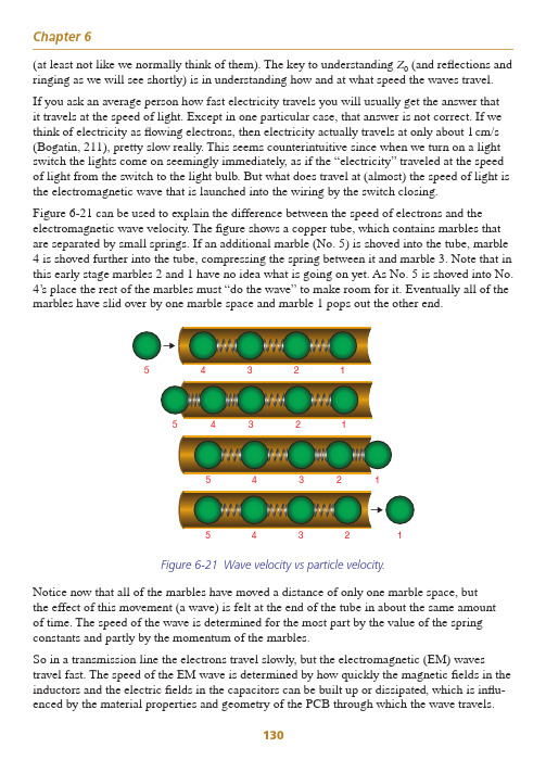
Figure 6-41 Setting the trace spacing in Layout.Traces with acute and 90؇ anglesRouting high-frequency analog or high-speed digital traces with acute or 90Њ angles has long been discouraged, but not everyone agrees anymore as to how much of a problem it really isThe Select tool is used to select pins, text, or any of the graphical objects (lines, arcs, etc.). The Snap-to-Grid function is actually a coarse or fiObjects can be selected by fully enclosing the object with a selection box (using the SelectThe Place Pin tool is used to place pins on a part one at a time.Place Pin Array toolThe Array tool is used to simultaneously place multiple pins on a part such as a 16-bit outputPlace Line toolThe Line tool is used to place a single orthogonal or diagonal line segment.Place Polyline toolThe Polyline tool is used to place multisegment lines. Polylines are orthogonal by default, butPlace Rectangle toolUsed to place closed rectangular parallelograms.Place Ellipse toolUsed to place circles and ellipses.Place Arc toolPlace Text toolUsed to place text objects, which have font, color, and rotation settings.Zoom InZooms in by set increments. YZoom OutZoom to RegionUse this tool to zoom to a particular region of your design by dragging a box around the area Zoom to AllFigure 7-3 Single-part, homogeneous transformer and schematic.Figure 7-4 Starting a new part from a new Capture library.New Part Properties dialog box will open as shown in Fig. 7-6. Enter a name for the part (for example, XFMR S_Pri:CT_Sec) and “T” for the reference prefi x. Ypins and graphical objects are placed on the grid. The snap-to-grid setting can be changed, or off, . The default grid is shown as dots, butFigure 7-5 Beginning a new part from the Library Manager.Figure 7-6 New Part Properties dialog box.Figure 7-8 Grid settings in Options→Preferences dialog box.The next step is to add the pins that will make the transformer’. TheFigure 7-9 The Place Pin dialog box.for the pin shape and Passive for the pin type; click OK. Place the fipins on the left side of the border at positions (0.0, 0.1) and (0.0, 0.5) for the primary windingFigure 7-10 Use the Browse Spreadsheet dialog box to modify pin parameters. The next step is to place graphics to build the transformer coils. Turn the Snap to Grid (toggle the button so that it turns red). Select the Place Arc tool, . Arcs are defi ned by three points as shown in Fig. 7-11. The fi nes the center of the arc,, toggle the Select tool, , select the objects you want to copy. Left click once to select a single object, or use CtrlNext, place two parallel lines between the arcs to represent the core. Use the Place Line tool, , to draw them. Then make the dots for the dot–coil indicator by using the Place Ellipse tool, . Draw a small circle near one of the coils, then hit theChange the circle to a fiFigure 7-12 Use the Edit Filled Graphic dialog box to fi ll objects with patterns.Figure 7-13 Completed part with pin names and numbers visible.Figure 7-13 shows the transformer design so far. Note that the pin numbers are on the pin outside the boundary and pin names are inside the boundary with the graphics.Figure 7-14 User Properties dialog box from Options→Part Properties menu.(a) User Properties dialog box (Part Properties). (b) Edit Properties dialog box(Package Properties).Completed homogeneous part (pin names and numbers not visible).nal task is to save the new part (and the library if it is new). To save the part part editing window and click Yes at the Save changes to part name? prompt.Library icon in the Project Manager, right click, and select。
用PROTEUS设计制作印刷电路板

用PROTEUS设计制作印刷电路板摘要:这份论文介绍了如何使用PROTEUS软件设计和制作印刷电路板(PCB),包括电路设计、尺寸布局、线路距离等相关内容。
通过PROTEUS软件,可以轻松生成PCB原理图,并进行切片的导出,最终生成PCB制造所需的Gerber文件。
本文将详细介绍PROTEUS软件在PCB设计和制造过程中的具体操作步骤。
关键词:PROTEUS,印刷电路板,设计,制作,Gerber文件正文:一、引言PCB(Printed Circuit Board)电路板是电子产品中非常重要的一个组成部分,其作用相当于各种元器件的桥梁,它将每个元器件之间的连接点通过导线和电路板来进行连接,使电路得以工作。
PCB通常由纸片和玻璃纤维布层嵌合而成。
为了方便大规模制造和维修,现在的电路板都采用机器制造加工,即通过将电路确定下来并进行自动化加工的方式来生产。
在这个过程中,PROTEUS软件则具有至关重要的作用。
下面,本文将详细介绍如何使用PROTEUS软件进行PCB的设计和制造过程。
二、PROTEUS软件介绍PROTEUS是一款由英国Labcenter开发的软件,主要用于虚拟设计和仿真电路。
利用该软件,电子工程师可以在一个完整的虚拟环境中完成电路设计、仿真和制造等一系列工作。
其中,PCB设计就是PROTEUS的其中之一重要的功能。
三、PCB设计步骤1. 建立 PCB 原理图首先,我们需要在PROTEUS中创建一个新的PCB工程。
为此,我们可以在“File > New Project”中选择“PCB Design”作为工程类型。
接着,我们需要在Proteus ISIS中进行PCB原理图设计,即将电路板上的各元件、线路、电源接口等添加进去,并设置它们之间的连接方式。
完成原理图设计后,我们还可以通过PROTEUS自带的随机填充功能,快速初始化PCBLayout中的线路位置。
2. 进行尺寸布局PCB原理图设计完成后,我们就需要按照设计要求进行PCB的尺寸布局,这是为了确保最终的线路完美贴合到PCB板上。
印刷电路板设计

印刷电路板设计印制电路板设计也称印制板排版设计,通常包括设计预备、形状及结构草图设计、设计布局、设计布线、提出加工工艺图及技术要求等过程:1.设计预备了解电路工作原理和组成,各功能电路的相互关系及信号流向等内容,对电路工作时可能发热、可能产生干扰等状况心中有数。
了解印制板工作环境(是否密封,工作环境温度变化,是否有腐蚀性气体等)及工作机制(连续工作还是断续工作等)。
熟识主要电路参数(最高工作电压,最大电流及工作频率等)。
了解主要元器件和部件的型号、形状尺寸、封装,必要时取得样品或产品样本。
2.形状及结构草图设计(1)对外连接草图,它是依据整机结构和分板要求确定的,一般包括电源线、地线板外元器件的引线、板与板之间连接线等,绘制草图时应大致确定其位置和排列挨次。
若采纳接插件引出时,要确定接插件位置和方向。
(2)印制板形状尺寸草图:印制板形状尺寸受各种因素制约,一般在设计时已大致确定,从经济性和工艺性动身,优先考虑矩形。
印制板的安装、固定也是必需考虑的内容,印制板与机壳或其他结构件连接的螺孔位置及孔径应明确标出。
3.设计布局布局就是将电路元器件放在印制板有线区内,布局是否合理不仅影响布线工作,而目对整个电路板的性能也有重要作用。
这里对布局要求、原则、布放挨次作一简要介绍。
(1)布局要求:首先要保证电路功能和性能指标。
在此基础上满意工艺性,检测、修理方面的要求。
同时,适当兼顾美观性,元器件排列整齐疏密得当。
(2)布局原则:(a)就近原则,相关电路部分应就近安放,避开走远路,绕弯子。
(b)信号流原则,按电路信号流向布放,避开输入输出,凹凸电平部分交叉。
(c)散热原则,有利于发热元器件散热。
(3)布放挨次。
(a)先大后小,先安放占面积较大的元器件;先集成后分立;(b)先主后次,多块集成电路时先放置主电路。
(4)布局方法:(a)实物法。
将元器件和部件样品在1:1的草图上排列,查找最优布局。
实际应用中一般是将关键的元器件或部件实物作为布局依据。
印刷电路板设计制作
印刷电路板设计制作印刷电路板(Printed Circuit Board,简称PCB)是电子产品中不可或缺的部件。
它是一种用于连接电子元件之间的导电板,可以将复杂的电路结构压制在一个小巧的板上。
在电路板的设计和制作中,需要一定的技能和经验,本文将简单介绍印刷电路板的设计和制作流程。
PCB的基本结构PCB通常包括顶层(Top layer)、底层(Bottom layer)、中间层(Inner layer)和密码层(Solder mask)等几个部分。
其中顶层和底层都是铜质的,用于承载电路元件和传递电信号。
而中间层也是铜质的,但是通常用于连接顶层和底层之间的电路。
密码层则是一层特殊的涂层,与铜质层之间隔开,用于保护电路和防止短路。
PCB的设计流程第一步:确定电路设计在进行PCB设计之前,需要确定电路设计,包括电路需要具备的功能和要用到的元器件等。
设计师需要根据电路设计图纸或者电路原理图,确定需要连接的线路、电气元件和机械连接。
第二步:选择设计软件在进行PCB设计时,需要选择符合要求的设计软件。
目前常用的PCB设计软件有Eagle、Altium Designer、PADS、KiCad、OrCAD等。
第三步:创建PCB板图根据电路设计图纸或者电路原理图,在PCB设计软件中创建PCB板图。
具体操作包括:从元件库中选择需要用到的元件;将元件拖拽到PCB板图中合适的位置;利用软件自带的连接功能进行线路的连接;布局好PCB板图中的各元件。
第四步:布线将PCB板图中的各元件按照电路设计图纸或者电路原理图的线路连接,完成PCB布线。
在布线过程中,需要注意元件之间的距离和线路的宽度,以避免短路和漏电等问题。
第五步:添加标记和注释在PCB设计过程中,需要添加标记和注释,以方便制造和维修。
标记主要包括器件编号、引脚类型、元件名称等信息。
注释则可以说明电路的作用、特点等。
第六步:输出Gerber文件在完成PCB设计后,需要将设计资料输出成Gerber文件,以便制造厂商进行生产。
印刷电路板的基本设计方法和原则要求
印刷电路板的基本设计方法和原则要求印刷电路板(Printed Circuit Board,PCB)是电子设备中的重要组成部分,它起到了电子元器件的安装、连接和支撑作用。
在印刷电路板的基本设计中,需要考虑一系列的方法和原则要求。
以下是关于印刷电路板的基本设计方法和原则要求的详细介绍。
一、电路板的尺寸和形状设计方法和原则要求:1.尺寸设计:在设计电路板尺寸时,需要根据具体的应用需求来确定。
同时,也需要考虑到电路板的组装和安装方便性,以及电磁兼容性等因素。
2.形状设计:常见的电路板形状包括矩形、方形、圆形等。
形状设计需要与设备的外壳和周围空间相匹配,以确保电路板能够完美地安装和连接。
二、电路板层数和布局方法和原则要求:1.层数设计:电路板的层数是指电路板上的金属层的数量,通常有单面板、双面板和多层板。
在设计时,需要根据电路复杂性和布局的要求来决定电路板的层数。
2.布局设计:电路板的布局设计是非常重要的环节。
在布局过程中,应合理安排各个元器件的位置和电路的走线,以最大程度地减少电磁干扰和信号串扰,并实现电路的紧凑布局。
三、电路板原理图和元器件选型方法和原则要求:1.原理图设计:原理图是电路板设计的基础,需要准确地反映电路的功能和连接关系。
在设计原理图时,需要符合标准的电路图符号和约定,以方便后续的布线和制板工作。
2.元器件选型:在选择元器件时,需要根据电路的需求来进行选型。
选型时需要考虑元器件的性能指标、尺寸、工作温度、可靠性等因素,以保证电路的正常工作和长期稳定性。
四、电路板布线和走线方法和原则要求:1.布线设计:布线设计是电路板设计中最重要的步骤之一、在布线时,需要根据原理图的要求,合理地安排信号线和电源线的布置,以最小化信号串扰和电磁干扰的影响。
2.走线原则:在进行走线时,需要遵循以下原则:(1)尽量使用直线走线,减少走线的弯曲和交叉;(2)多层板应合理利用内层的走线空间;(3)保持走线的等长性,避免信号的传输时间差;(4)对重要信号线和高频信号线进行隔离和屏蔽。
PCB印刷电路板设计
6 元件封装图的修改和创建
• 以上PCB设计中我们看到,尽管Protel99的元件封装库十分庞大,但 经常找不到我们需要的元件封装,或不合我们的要求,如上述电路中, 我们就未找到适合发光二极管的封装图,这就需要我们自己修改或创建 适合我们需要的元件封装图,在这方面,Protel99有着十分强大的功能, 操作起来也十分简单方便。 • 1.修改元件封装图 • 以修改电容封装为例,通过PCB设计窗口左边的元件封装浏览器找 到要修改的元件封装,这里,我们找一个封装为RB.4/.8的电容为修改对 象,单击下面的Edit按钮,进入封装图形编辑器,发现其两焊盘间的距 离为10mm,与我们所用电容管脚的间距2.5mm相差较大,需对其进行调 整,可直接用光标拖动焊盘2至焊盘1 2.5mm处,此时,两焊盘因直径较 大,碰在一起,双击任一个焊盘,在弹出的焊盘编辑对话框中,将焊盘 X、Y方向尺寸改为2mm,按一下 (通用)按钮,再按OK键, 焊盘修改完成。接着将圆圈改小一点,双击圆圈边缘,在弹出的对话框 中将圆的半径修改为4mm,按OK确定。最后,还应将其重命名为 RB2.5/8,保存后退出。
类型的选项可改变尺寸标注的方式,如图:
PCB设计综合练习
PCB设计综合练习
• 参考下图,按要求完成PCB板的布线设计:
1. 线宽:正负电源线:1mm, LED支路:见图中箭头标注, 其余0.35mm。 电路板圆角半径:3.5mm。 定位孔直径:5mm,定位孔 位置见图中坐标点的标注。 不同的操作一定要在不同的 层面进行,如画板框在 层,布线在 层,画 定位孔在 层等。
顶层
底层
丝印层
复合层
机械加工层
禁止布线层
5.3 PCB板外形尺寸设计
• 此项操作在禁止布线层KeepOutLayer进行,需 将层标签页切换至该层,再按如下步骤进行:
印刷电路板设计(精品)共129页

ቤተ መጻሕፍቲ ባይዱ 21、要知道对好事的称颂过于夸大,也会招来人们的反感轻蔑和嫉妒。——培根 22、业精于勤,荒于嬉;行成于思,毁于随。——韩愈
23、一切节省,归根到底都归结为时间的节省。——马克思 24、意志命运往往背道而驰,决心到最后会全部推倒。——莎士比亚
25、学习是劳动,是充满思想的劳动。——乌申斯基
谢谢!
印刷电路板设计(精品)
31、别人笑我太疯癫,我笑他人看不 穿。(名 言网) 32、我不想听失意者的哭泣,抱怨者 的牢骚 ,这是 羊群中 的瘟疫 ,我不 能被它 传染。 我要尽 量避免 绝望, 辛勤耕 耘,忍 受苦楚 。我一 试再试 ,争取 每天的 成功, 避免以 失败收 常在别 人停滞 不前时 ,我继 续拼搏 。
33、如果惧怕前面跌宕的山岩,生命 就永远 只能是 死水一 潭。 34、当你眼泪忍不住要流出来的时候 ,睁大 眼睛, 千万别 眨眼!你会看到 世界由 清晰变 模糊的 全过程 ,心会 在你泪 水落下 的那一 刻变得 清澈明 晰。盐 。注定 要融化 的,也 许是用 眼泪的 方式。
35、不要以为自己成功一次就可以了 ,也不 要以为 过去的 光荣可 以被永 远肯定 。
- 1、下载文档前请自行甄别文档内容的完整性,平台不提供额外的编辑、内容补充、找答案等附加服务。
- 2、"仅部分预览"的文档,不可在线预览部分如存在完整性等问题,可反馈申请退款(可完整预览的文档不适用该条件!)。
- 3、如文档侵犯您的权益,请联系客服反馈,我们会尽快为您处理(人工客服工作时间:9:00-18:30)。
Figure 9-15 Final BOM listing with all footprints assigned.ou can also use the Find tool to automatically select a part or parts of a certain type. To useFigure 9-16 Using the Find tool to locate parts.Grouping related componentsFigure 9-17 Using the Property Editor to assign components to groups.To view group information for the entire design go to the Project Manager and select Design icon. Right click and select Part Manager from the pop-up (or select Part Figure 9-18 Using the Part Manager to view all groups.Figure 9-19 The Confi gure Part Property Display dialog box.ou can also add the COMPGROUP property to the bill of materials listing by adding “\tCOMPGROUP” to the Header: list and “\t{COMPGROUP}” to the Combined PropertyFigure 9-20 Performing a design annotation.Warning!■ Do not perform another annotation after you have generated a Layout netlist or performed a back annotation from Layout (especially if you had Layout renumber the parts), because the project can become unsynchronized and produce verypeculiar, irreversible results! To read more about the annotation function, searchFigure 9-21 The Capture Design Rules Check dialog box.Figure 9-22 Creating a circuit netlist for Layout from Capture.Defi ning the board requirementsOne of the fi rst steps in setting up a new board in Layout is to select a technology fi le, which requires deciding on a couple of design requirements up front. Choosing a technology fi le requires knowing what types of parts will be used in the design (packaging and assem-bly requirements), the number and type of layers required, and the trace width and spacing requirements. These considerations for the analog design example are discussed in the follow-Figure 9-23 Layer stack-up for Example 1.Figure 9-24 Using the AutoECO to begin a new PCB design in layout.rst view you have of your new board will probably be a black background and part of a red square. Click the Zoom All button, so that you can see the entire design. Y ou should see something similar to Fig. 9-27.Setting up the boardMaking a board outlinerst step in laying out the board is to make the board outline and add mounting holes so that the boundaries of the board are known. First turn off the DRC box by toggling theFigure 9-25 Example of the AutoECO Link Footprint error. Figure 9-26 Adding a footprint library to the AutoECO tool’s library list.Figure 9-27 Initial view of the analog design.Online DRC button, located on the toolbar. Then, draw a board outline: select the Obstacle tool, . Right click in the work space and select New from the pop-up, right click again, and select Properties to invoke the Edit Obstacle dialog box. Make sure the obstacle Board outline on the Global layer. Click OK.Left click at point 0,0 to place the fi rst vertex. Left click to place each vertex of the board outline. Make the board outline about 2.0 ϫ 2.5 in. (2000 ϫ 2500 mils). Right click and select Finish from the pop-up after you have placed the fourth vertex.Next, place mounting holes on the board. This should be done before moving any parts intoselect the Component tool, right click, anddialog box shown in Fig.Figure 9-28 Using Edit Component dialog box to add mounting holes.Figure 9-29 Adding a mounting hole to a net.The mounting holes supplied with Layout are plated by default. To make mounting holes , toggle the Pin tool and select the mounting hole’s padstack (useFigure 9-30 Use the Edit Padstack dialog box to make a padstack nonplated. connectors, etc. Dimensions can be placed on assembly or comment layers (e.g., the layer). Once you are satisfi ed with the board layout, you can turn off documentation layers and/or delete temporary dimension lines.Adding dimensions and measurements is a three-step process. Each step is accomplished Tools →Dimension menu (see Fig. 9-31) and is used to (1) specify the snap settings, (2) specify the type of dimension, and fi nally (3) place the dimension.Figure 9-32 shows examples of relative and absolute dimensions. Relative dimensionsFigure 9-31 Setting up and placing dimension lines.5002000There are two ways to turn off the rat’s nest. This just makes the nets look invisible and does not actually affect their connectivity. The second way is to actually disable the nets (which affects bothFigure 9-33 Using the Find function to select parts for placement.To select certain parts without having to actually fi nd them in the pile, you can have a partFigure 9-34 Using Component Selection Criteria to select parts for placement.Placing parts in the queueAn elegant way to place parts is to make a placement list to queue parts for placement. Then all you need to do is hit N on your keyboard to cycle through the list. Y ou can add parts to the placement queue using the Tool →Component →Queue For Placement... optionFigure 9-35 Selecting parts from the placement matrix.as a minipile. To place the parts, left click inside the board outline in the location where the parts should go. The parts within the group will be stacked on top of each other like football To enable and disable netsbutton, and selectFig. 9-36) by selecting (highlighting) a net (or nets). Right click and toggle theFigure 9-36 Enabling and disabling nets.10 R11Figure 9-39 Default layer stack-up.Converting a routing layer to a plane layerThere are two ways to add plane layers. The fi rst method is to convert a routing layer into a plane layer. The second method is to add a new plane layer based on the properties of anFigure 9-40 Converting a routing layer to a plane layer.Note■ Do NOT change the Layer NickName. The layer nickname is associated with aFigure 9-41 Layer setup that defi nes the six-layer stack-up.Assigning nets to layersThe next step is to assign the power and ground nets to their respective plane layers. To assign ground and power nets to plane layers click the View Spreadsheet button and select Nets from the pop-up to open the Nets spreadsheet. Select the GND net and then right click and select Properties from the pop-up. In the Edit Net dialog box (Fig. 9-42), click the Net Layers... button in the lower left corner. In the Layers Enabled for RoutingFigure 9-42 Assigning power/ground nets to plane layers.Repeat the procedure and assign the Vϩ and VϪ nets to the Vϩ and VϪ plane layers, respec-tively, and include the TOP and BOTTOM layers. Y ou should now see YES* in the Routing Enabled column of the spreadsheet for each of the plane layers (at least before performing aFigure 9-43 Assigning alternate vias to a net.ou can select more than one via for the autorouter to use, but you also need to let Layout know it is allowed to use other vias than the default via. Go to Options →Route Settings to display the Route Settings dialog box (Fig. 9-44). Check the Use All Via Types option.Figure 9-44 Route Settings dialog box to specify via usage.Open the Nets spreadsheet and drag a box across all of the nonpower and nonground nets (cells) to select them. Right click and select Enable Ͻ-ϾDisable from the pop-up to toggle off the selected nets. Close the spreadsheet.On your board layout you should notice that some of the rat’s nest lines (nets) have disap-peared. The only lines you should see are the power and ground lines. To identify which lines are which, enable one of the routing tool buttons (Add/Edit Route Mode, forleft click and select one of the nets. In the bottom left corner of your. More lines will disappear. The lines that disappear are ones that are connected to through-hole pins that are connected to their respective plane layersFigure 9-45 Specifying fanout settings.through the layer list. Each pin that is connected to a plane layer will have a thermal relief around it as that layer is made active as shown in Fig. 9-46. The lines that did not disappear are not connected to a plane yet because the surface-mount devices do not have a way toget to the plane(s). So the next step is to provide paths (called fanouts or stringers) for the surface-mount devices to become connected to their planes.Fanning out power and groundNormally it is recommended that power and ground are fanned out separately and that ground rst. Ground can usually be fanned out using the automatic fanout feature butbutton. The DRC should report about 19 errors. The errors are marked on the board by circledFigure 9-51 Viewing Error Markers.The list of errors may look formidable, but as you will soon see, one problem often causes several errors. By looking for patterns between the comments on the error spreadsheet and the layers on which the errors have occurred, you should be able to get an idea of the problems.activate the Pin tool,PadstacksFigure 9-52 Errors caused by padstack settings on a defi ned plane layer.Changing padstack propertiesTo change pad dimensions manually double click the cell for the VϪ layer, right click, and select Properties to display the Edit Padstack Layer dialog box. Change the Pad WidthFigure 9-53 Copying plane-type padstack layers.If the second ground plane had been generated by converting another routing layer (INNER2, for example) into a plane layer it would have had the same errors and the same process could x the errors (i.e., copy all GND padstack layers into the GND2 padstackbutton, . Once the DRC box (the dotted rectangle) is displayed you can change the size and starting box being drawn, the view will also be zoomed to the size of the new DRC box. To zoom outbutton, or hit thezoomed back out, but the size of the DRC box will be unchanged.Figure 9-55 Board statistics spreadsheet. Figure 9-56 Clearing Route Pass fl ags to redo autoroute.Figure 9-57 Setting up back annotation settings in Capture.On the schematic in Capture double click on the part that you looked at before you did the back annotation and see how the spreadsheet has changed. The locations and orientation of the parts on the board (and any new footprints, etc.) will be listed in Capture. If you want (or need) to start a new board layout, all of this information will be included with the .MNLFigure 9-58 Forward annotation warning.Figure 9-60 Connection of the analog and digital grounds.leave the board separately and be connected at the power supply, or they may be connected at a pin (or pins) and leave the board together as one common ground. In this example the two grounds are connected at pin 5.To place the analog and digital ground symbols use the Place Ground tool, and select the desired ground symbols. To change the symbol’s name select the ground symbolFigure 9-61 (a) Change a ground/power symbol’s name and (b) display it.Figure 9-62 Select ground net name (analog or digital).It appears on the schematic that the analog and digital grounds are separate ground systemsBusses are placed on the schematic using the Place Bus tool, . After you have placed the ne (name) it with an alias using the Place Net Alias tool, . Busses are namedis the alias (a name you give it) that make up the members are placed on the schematic using the Place Wire tool, members are placed on the schematic as you would place any other wire, but they are addedbutton, , from the toolbar and place no-connect symbols on the unused pins.。