RXT-090505中文资料
RUZ-050505;RUZ-050505P;中文规格书,Datasheet资料
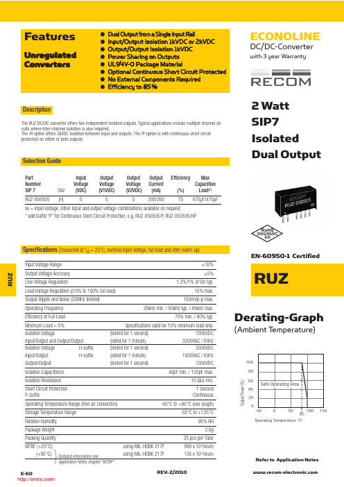
E-60REV: 2/2010Refer to Application NotesECONOLINEDC/DC-Converterwith 3 year WarrantyRUZEN-60950-1 CertifiedPart Input Output Output Output Efficiency Max Number Voltage Voltage Voltage Current Capacitive SIP 72kV (VDC)(V1VDC)(V2VDC)(mA)(%)Load (1)RUZ-050505(H)555200/20070470µF/470µFxx = Input Voltage. Other input and output voltage combinations available on request.* add Suffix “P” for Continuous Short Circuit Protection, e.g. RUZ-050505/P , RUZ-050505/HPO u t p u t P o w e r (%)100602040Operating Temperature °C0802 Watt SIP7 Isolated Dual OutputDerating-Graph(Ambient T emperature)●Dual Output from a Single Input Rail●Input/Output Isolation 1kVDC or 2kVDC ●Output/Output Isolation 1kVDC ●Power Sharing on Outputs ●UL94V-0 Package Material●Optional Continuous Short Circuit Protected ●No External Components Required ●Efficiency to 85%FeaturesUnregulated ConvertersInput Voltage Range±10%Output Voltage Accuracy ±5%Line Voltage Regulation1.2%/1% of Vin typ.Load Voltage Regulation ((10% to 100% full load)15% max.Output Ripple and Noise (20MHz limited)150mVp-p max.Operating Frequency 20kHz min. / 50kHz typ. / 85kHz max.Efficiency at Full Load70% min. / 80% typ.Minimum Load = 0%Specifications valid for 10% minimum load only.Isolation Voltage(tested for 1 second)1000VDC Input/Output and Output/Output (rated for 1 minute)3200VAC / 60Hz Isolation Voltage H-suffix (tested for 1 second)2000VDC Input/Output H-suffix (rated for 1 minute)1000VAC / 60Hz Output/Output (tested for 1 second)1000VDCIsolation Capacitance 40pF min. / 120pF max.Isolation Resistance 10 G Ωmin.Short Circuit Protection 1 Second P-SuffixContinuousOperating Temperature Range (free air convection)-40°C to +85°C (see Graph)Storage Temperature Range -55°C to +125°CRelative Humidity 95% RH Package Weight 2.8gPacking Quantity 25 pcs per Tube MTBF (+25°C)using MIL-HDBK 217F988 x 103 hours (+85°C)using MIL-HDBK 217F135 x 103hoursSelection Guide}Detailed Information seeApplication Notes chapter "MTBF"Specifications (measured at T A = 25°C, nominal input voltage, full load and after warm-up)The RUZ DC/DC converter offers two independent isolated outputs. Typical applications include multiple channel cir-cuits where inter-channel isolation is also required.The /H option offers 2kVDC isolation between input and outputs. The /P option is with continuous short circuit protection on either or both outputs.DescriptionR U ZRoHS2002/95/EC6/6/Package Style and Pinning (mm)Dual Independent Outputs3rd angle projectionRecommended Footprint Details7 PIN SIP PackageXX.X ± 0.5 mm XX.XX ± 0.25 mmPin Connections Pin #Single1 +Vin2 –Vin4 +Vout 15–Vout 16 +Vout 27–Vout 2Typical CharacteristicsRUZ SeriesECONOLINEDC/DC-ConverterE f f i c i e n c y %10040%0%100%40Efficiency / Load 60%80%20%206080Total Output current (%)Deviation / Load-10.00040%0%100%D e v i a t i o n f r o m N o m i n a l (%)60%80%20%-5.000Total Output current (%)0.0005.00010.00015.00020.00025.000DCDC1Channel 1RUZ-050505DC2Channel 2REV:2/2010E-61 RUZTypical ApplicationNotes Note 1Maximum capacitive load is defined as the capacitive load that will allow start up in under 1 second without damage to the converter.Certifications EN General SafetyReport: PS-R7219C1EN60950-1:2001 + A11:2004/分销商库存信息:RECOM-POWERRUZ-050505RUZ-050505/P。
T912-A40K-005-05中文资料
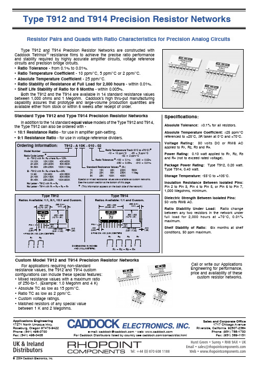
® resistance films to achieve the precise ratio performance Caddock Tetrinox® MG 650 Caddock Tetrinox resistance films to achieve thesource precise ratio performance ® resistance and stability required by highly accurate amplifier circuits, reference Caddock's Micronox films are the ofvoltage Preconditioning for Power and Voltage Ratings and stability required by highly accurate amplifier circuits, reference and stability required by highly accurate amplifier circuits,voltage voltage reference MG 655 Now with Extended Resistance Range to 10,000 Megohms and Additional Models circuits and precision bridge circuits. the
CR2015RJ005资料
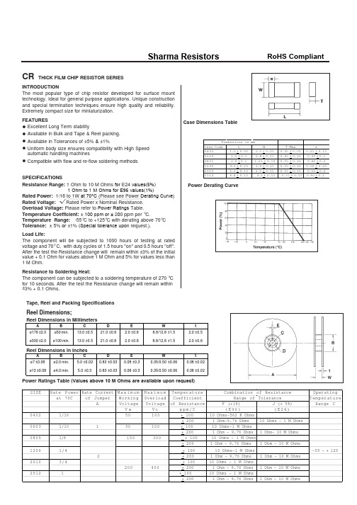
Sharma Resistors CR
THICK FILM CHIP RESISTOR SERIES
RoHS Compliant
INTRODUCTION The most popular type of chip resistor developed for surface mount technology. Ideal for general purpose applications. Unique construction and special termination techniques ensure high quality and reliability. Extremely compact size for miniaturization. FEATURES Excellent Long Term stability Available in Bulk and Tape & Reel packing. Available in Tolerances of ±5% & ±1% Uniform body size ensures compatibility with High Speed automatic handling machines Compatible with flow and re-flow soldering methods
• • • • •
Case Dimensions Table
SPECIFICATIONS Resistance Range: 1 Ohm to 10 M Ohms for E24 values(5%) 1 Ohm to 1 M Ohms for E96 values(1%) Rated Power: 1/16 to 1W at 70°C (Please see Power Derating Curve) Rated Voltage: Rated Power x Nominal Resistance. Overload Voltage: Please refer to Power Ratings Table. Temperature Coefficient: ± 100 ppm or ± 200 ppm per °C. Temperature Range: -55°C to +125°C with derating above 70°C Tolerance: ± 5% or ±1% (Special tolerance upon request.). Load Life: The component will be subjected to 1000 hours of testing at rated voltage and 70° C, with duty cycles of 1.5 hours ''on'' and 0.5 hours ''off''. After the test the Resistance change will remain within ±3% of the initial value + 0.1 Ohm for values above 1 M Ohm and 5% for values less than 1 M Ohm. Resistance to Soldering Heat: The component can be subjected to a soldering temperature of 270 °C for 10 seconds. After the test the Resistance change will remain within ±3% + 0.1 Ohms. Tape, Reel and Packing Specifications
MSA-0505中文资料
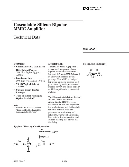
Cascadable Silicon Bipolar MMIC␣Amplifier Technical DataFeatures•Cascadable 50 Ω Gain Block •High Output Power:18.0 dBm Typical P 1 dB at 1.0␣GHz •Low Distortion:29.0 dBm Typical I P 3 at 1.0␣GHz •7.0 dB Typical Gain at 1.0␣GHz •Surface Mount Plastic Package •Tape-and-Reel Packaging Option Available [1]MSA-050505 Plastic PackageDescriptionThe MSA-0505 is a high perfor-mance medium power silicon bipolar Monolithic Microwave Integrated Circuit (MMIC) housed in a low cost, surface mount package. This MMIC is designed for use as a general purpose 50 Ωgain block. Typical applications include narrow and broad band IF and RF amplifiers in commercial systems.The MSA-series is fabricated using HP’s 10 GHz f T , 25␣GHz f MAX ,silicon bipolar MMIC process which uses nitride self-alignment,ion implantation, and gold metalli-zation to achieve excellent performance, uniformity and reliability. The use of an external bias resistor for temperature and current stability also allows bias flexibility.Typical Biasing ConfigurationRV CC > 12 VINOUTNote:1.Refer to PACKAGING section “Tape-and-Reel Packaging for Semiconductor Devices.”MSA-0505 Absolute Maximum RatingsParameter Absolute Maximum [1]Device Current135 mA Power Dissipation [2,3] 1.5 W RF Input Power+25 dBm Junction Temperature 200°C Storage Temperature–65 to 150°CThermal Resistance [2,4]:θjc = 85°C/WNotes:1.Permanent damage may occur if any of these limits are exceeded.2.T CASE = 25°C.3.Derate at 11.8 mW/°C for T C > 73°C.4.See MEASUREMENTS section “Thermal Resistance” for more information.P 1 dB Output Power at 1 dB Gain Compression f = 0.5 GHz dBm 19.0f = 1.0 GHz dBm 16.018.0G P Power Gain (|S 21|2) f = 0.5 GHz dB7.5f = 1.0 GHz 6.07.0∆G P Gain Flatness f = 0.1 to 1.5 GHzdB ±0.75f 3 dB 3 dB Bandwidth [2]GHz2.3I nput VSWR f = 0.1 to 1.5 GHz 1.6:1Output VSWRf = 0.1 to 1.5 GHz 2.0:1I P 3Third Order Intercept Point f = 1.0 GHz dBm 29.0NF 50 Ω Noise Figure f = 1.0 GHz dB 6.5t D Group Delay f = 1.0 GHz psec 190V d Device VoltageV 6.78.410.1dV/dTDevice Voltage Temperature CoefficientmV/°C–16.0Notes:1.The recommended operating current range for this device is 60 to 100 mA. Typical performance as a function of current is on the following page.2.Referenced from 0.1 GHz Gain (G P ).Electrical Specifications [1], T A = 25°CSymbolParameters and Test Conditions: I d = 80 mA, Z O = 50 ΩUnitsMin.Typ.Max.VSWR Part Number Ordering InformationPart Number No. of DevicesContainer MSA-0505-TR15007" Reel MSA-0505-STR10StripFor more information, see “Tape and Reel Packaging for Semiconductor Devices”.MSA-0505 Typical Scattering Parameters (T A = 25°C, I d = 80 mA)Freq.MHzMagAngdBMagAngdBMagAngMagAngk5.56–3914.9 5.56161–18.5.12039.65–360.6025.24–1039.7 3.05156–13.9.20212.25–900.9750.15–1308.2 2.57163–13.7.2077.15–116 1.15100.13–1557.8 2.45165–13.7.2073.11–132 1.21200.12–1707.7 3.43161–13.5.2111.11–145 1.21400.121787.5 2.37148–13.6.209–1.14–146 1.23600.131727.4 2.34134–13.6.209–2.17–151 1.23800.131687.2 2.29119–13.6.209–3.21–157 1.231000.141667.0 2.24105–13.4.213–4.25–164 1.211500.21159 6.4 2.0972–13.3.217–6.34176 1.162000.30148 5.2 1.8242–13.1.222–9.42159 1.122500.40136 4.1 1.6017–12.9.227–11.48146 1.053000.52121 2.7 1.36–7–12.6.234–16.551330.92A model for this device is available in the DEVICE MODELS section.S 11S 21S 12 S 22Typical Performance, T A = 25°C(unless otherwise noted)24681081012141618202224POWER OUT (dBm)Figure 1. Typical Gain vs. Power Out,T A = 25°C, I d= 80 mA.G A I N (d B )FREQUENCY (GHz)Figure 2. Device Current vs. Voltage.306090120V d (V)I d (m A )36912121418162220P 1 d B (d B m )TEMPERATURE (°C)Figure 3. Output Power at 1 dB Gain Compression, vs. Case Temperature, I d = 80 mA.18–25+25+851434P 1 d B (d B m )I d (mA)Figure 5. Output Power at 1 dB Gain Compression, Third Order Intercept vs. Case Temperature, f = 1.0 GHz.Figure 4. Gain vs. Frequency,I d = 80 to 100 mA.60708090100I P 3 (d B m )0.5 GHz1.0 GHz2.0 GHz.01.050.10.5 1.05.014121086420G p (d B )05 Plastic Package Dimensions(4 PLCS)0.0005 ± 0.010 (0.013 ± 0.25)DIA Notes:(unless otherwise specified)1. Dimensions are in2. Tolerancesin .xxx = ± 0.005 mm .xx = ± 0.13mm。
RTD-0505HP中文资料

ECONOLINE
DC/DC-Converter
Specifications (Core Operating Area)
Reflow Temperature ROHS compliant (for more details see Application Notes) Relative Humidity Package Weight MTBF (+25°C) (+85°C) RTS types RTD types
RK-0905SHP中文资料
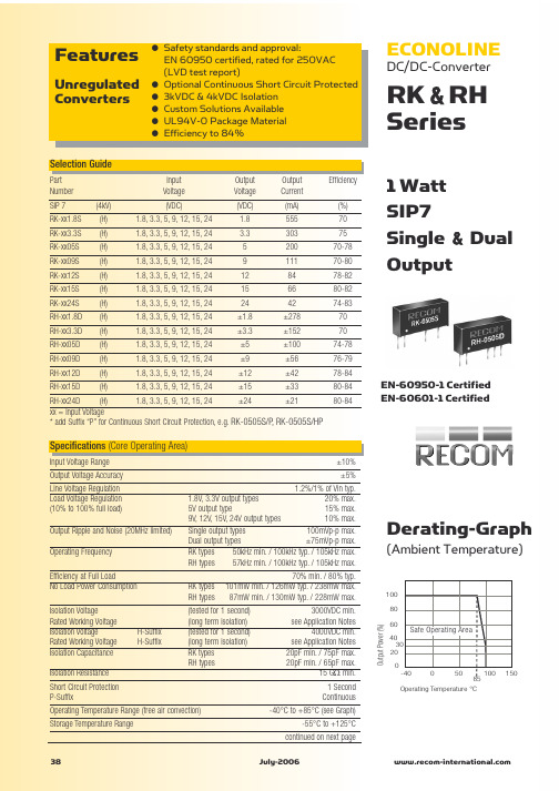
40 20 0
3.312
Efficiency %
20 0
0% 20% 40% 60% Total Output current (%)
80%
100%
0% 20% 40% 60% Total Output current (%)
80%
100%
0%
20%
40%
60%
80%
100%
Total Outputoad
25.000 20.000
Deviation / Load
Deviation from Nominal (%)
Deviation from Nominal (%)
15.000 10.000 5.000 0.000 -5.000 -10.000
15.000 10.000 5.000 0.000 -5.000 -10.000
Output Power (%)
60 40 30 20 0
Safe Operating Area
85 Operating Temperature °C
-40
0
50
100
150
元器件交易网
ECONOLINE
DC/DC-Converter
Specifications (Core Operating Area)
Derating-Graph
(Ambient Temperature)
100 80
H-Suffix H-Suffix
(tested for 1 second) (long term isolation) (tested for 1 second) (long term isolation) RK types RH types
PSD-0505中文资料

Copyright PEAK electronics GmbH
Partnumbers
PART NO. INPUT VOLTAGE (VDC) INPUT CURRENT FULL LOAD OUTPUT VOLTAGE (VDC) OUTPUT CURRENT (max. mA) EFFICIENCY FULL LOAD (% TYP.)
PSD-3R305S PSD-053R3S PSD-0505S PSD-0509S PSD-0512S PSD-123R3S PSD-1205S PSD-1209S PSD-1212S PSD-1215S
3.3 5 5 5 5 12 12 12 12 12
450 171 246 254 252 73 100 105 103 100
5 3.3 5 9 12 3.3 5 9 12 15
200 200 200 110 84 200 200 110 84 67
70 77 81 78 80 75 81 78 81 83
元器件交易网
Telefon: +49 (0) 6135 931069 Telefax: +49 (0) 6135 931070 www.peak-eltronics.de
SMD SERIES
PSD-XXXXS 1KV ISOLATED 1W UNREGULATED SINGLE OUTPUT SMD
Ambient Temperature ° C 85
1.00 W
Pin # 1 3 7 8 14
Connection Single - V Input + V Input - V Output + V Output NC
mt9045中文资料_数据手册_IC数据表

FS1
FS2
Figure 1 - Functional Block Diagram
Zarlink Semiconductor US Patent No. 5,602,884, UK Patent No. 0772912, France Brevete S.G.D.G. 0772912; Germany DBP No. 69502724.7-08
1
Zarlink Semiconductor Inc. Zarlink, ZL and the Zarlink Semiconductor logo are trademarks of Zarlink Semiconductor Inc.
Copyright 2003, Zarlink Semiconductor Inc. All Rights Reserved.
VSS
1
48 TMS
RST 2
47 TCK
TCLR 3
46 TRST
SECOOR 4
45 TDI
SEC 5
44 TDO
PRI 6
43 PRIOOR
Vdd 7
42 IC
OSCo 8
41 FS1
OSCi 9
40 FS2
Vss 10
39 IC
F16o 11 F0o 12
SSOP
38 37
RSEL MS1
RSP 13 TSP 14
TIE Corrector
Circuit
Virtual Reference
DPLL
Selected
Reference
Reference
Select
MUX
TIE
Corrector
T0505SH中文资料

T0505xH T0509xH®January 1995SENSITIVE GATE TRIACSSymbol ParameterValue Unit I T(RMS)RMS on-state current (360°conduction angle)Tc=100°C 5A I TSMNon repetitive surge peak on-state current (T j initial =25°C )tp =8.3ms 42Atp =10ms 40I 2t I 2t Value for fusingtp =10ms 8A 2s dI/dtCritical rate of rise of on-state currentI G =50mAdi G /dt =0.1A/µs.RepetitiveF =50Hz 10A/µs Non Repetitive50T stg T j Storage and operating junction temperature range -40,+150-40,+125°C TlMaximum lead temperature for soldering during 10s at 4.5mm from case260°C ABSOLUTE RATINGS (limiting values)I T(RMS)=5AV DRM =400V to 800V I GT ≤5mA to ≤10mAFEATURESSymbol ParameterVoltage Unit DM S N V DRM V RRMRepetitive peak off-state voltage T j =125°C400600700800VThe T05xxxH series of triacs uses a high performance MESA GLASS technology.These parts are intended for general purpose applications where gate high sensitivity is required.DESCRIPTIONA1GA2TO220non-insulated (Plastic)1/5P G (AV)=1W P GM =10W (tp =20µs)I GM =4A (tp =20µs)GATE CHARACTERISTICS (maximum values)Symbol ParameterValue Unit Rth(j-a)Junction to ambient 60°C/W Rth(j-c)Junction to case for D.C5.3°C/W Rth(j-c)Junction to case for A.C 360°conduction angle (F=50Hz)4°C/WTHERMAL RESISTANCES Symbol Test ConditionsQuadrant Sensitivity Unit0509I GT V D =12V (DC)R L =33ΩTj=25°C I-II-III-IV MAX 510mA V GT V D =12V (DC)R L =33ΩTj=25°C I-II-III-IV MAX 1.5V V GD V D =V DRM R L =3.3k ΩTj=125°C I-II-III-IV MIN 0.2V tgtV D =V DRM I G =40mA I T =7.1AdI G /dt =0.5A/µs Tj=25°CI-II-III-IVTYP2µs I H *I T =50mA Gate open Tj=25°C MAX 510mA I LI G =1.2I GTTj=25°CI-III-IV TYP 510mAIITYP 1020V TM *ITM=7.1A tp=380µs Tj=25°C MAX 1.65V I DRM I RRM V D =V DRM V R =V RRM Tj=25°C MAX 5µA Tj=110°C MAX 1.5mAdV/dt *VD=67%V DRM Gate open Tj=110°CMIN 20V/µsTYP10(dV/dt)c *(dI/dt)c =2.2A/msTj=110°C TYP12V/µs*For either polarity of electrode A 2voltage with reference to electrode A 1ELECTRICAL CHARACTERISTICS ORDERING INFORMATIONT0509M HTRIAC MESA GLASSCURRENTPACKAGE :H =TO220Non-insulated VOLTAGESENSITIVITYT0505xH /T0509xH2/51234501234567180O=180o=120o=90o=60o=30oT(RMS)I (A)P(W)Fig.1:Maximum RMS power dissipation versus RMS on-state current.1020304050607080901001101201300123456=180oTcase(C)oI (A)T(RMS)Fig.3:RMS on-state current versus case tempera-ture.2.62.42.22.01.81.61.41.21.00.80.60.4IgtTj(C)o Ih-40-20020406080100120140Igt[Tj]Igt[Tj=25C]oIh[Tj]Ih[Tj=25C]oFig.5:Relative variation of gate trigger current and holding current versus junction temperature.2040608010012014001234567-100-105-110-115-120-125Rth =0C/W5C/W 10C/W 15C/Wo o o o Tamb (C)oP (W)Tcase (C)o Fig.2:Correlation between maximum RMS power dissipation and maximum allowable temperature (Tamb and Tcase)for different thermal resistances heatsink +contact.1E-31E-21E-11E+01E+11E+25E+20.010.11Zth/Rth Zth(j-c)Zth(j-a)tp(s)Fig.4:Relative variation of thermal impedance versus pulse duration.11010010000510152025303540Tj initial =25CoNumber of cyclesI (A)TSM Fig.6:Non repetitive surge peak on-state current versus number of cycles.T0505xH /T0509xH3/51101101001000I (A).I 2t (A 2s)TSM Tj initial =25Co I TSMt (ms)I 2tFig.7:Non repetitive surge peak on-state current for a sinusoidal pulse with width :t ≤10ms,and cor-responding value of I 2t.0.51 1.52 2.53 3.54 4.50.1110100I (A)TM Tj initial25Co Tj maxV (V)TM Tj max Vto =0.95V Rt =0.090Fig.8:On-state characteristics (maximum values).T0505xH /T0509xH4/5Information furnished is believed to be accurate and reliable.However,SGS-THOMSON Microelectronics assumes no responsability for the consequences of use of such information nor for any infringement of patents or other rights of third parties which may result from its use.No license is granted by implication or otherwise under any patent or patent rights of SGS-THOMSON Microelectronics.Specifications mentioned in this publication are subject to chan ge without notice.This publication supersedes and replaces all information previously supplied.SGS-THOMSON Microelectronics products are not authorized for use as critical components in life support devices or systems without express written approval of SGS-THOMSON Microelectronics.©1995SGS-THOMSON Microelectronics -All rights reserved.SGS-THOMSON Microelectronics GROUP OF COMPANIESAustralia -Brazil -France -Germany -Hong Kong -Italy -Japan -Korea -Malaysia -Malta -Morocco -The NetherlandsSingapore -Spain -Sweden -Switzerland -Taiwan -Thailand -United Kingdom -U.S.A.PACKAGE MECHANICAL DATA TO220Non-insulated (Plastic)D G IHJB ALN1MNO PCFREF.DIMENSIONSMillimeters Inches Typ.Min.Max.Typ.Min.Max.A 10.30.406B 6.3 6.50.2480.256C 9.10.358D 12.70.500F 4.20.165G3.00.118H4.5 4.70.1770.185I 3.53 3.660.1390.144J 1.2 1.30.0470.051L 0.90.035M 2.70.106N 5.30.209N1 2.540.100O 1.21.40.0470.055P1.150.045Marking :type number Weight :1.8gT0505xH /T0509xH5/5。
R05J09中文资料

Dual Output TypesRxxG055/12±5±1007127RxxG095/12±9±557435DIP14 RxxG125/12±12±427542RxxG155/12±15±337641RxxG0524/48±5±10080/7045RxxG0924/48±9±557052/58DIP14 RxxG1224/48±12±427065/68RxxG1524/48±15±337070/75RxxH055/12±5±1007127RxxH095/12±9±557435SIP7 RxxH125/12±12±427542RxxH155/12±15±337641RxxH0524/48±5±10070/8045RxxH0924/48±9±557052/58SIP7 RxxH1224/48±12±427065/68RxxH1524/48±15±337070/75Absolute Maximum RatingsInput Voltage V IN5V types 7V typ.12V types 15V typ.24V types 24V typ.48V types48V typ.Short Circuit Duration 1)1s Internal Power Dissipation560mW Lead Temperature (1.5 mm from case for 10 seconds)300 °C1).Supply voltage must be discontinued at the end of the short circuit duration.Input Voltage Range V IN (continuous operation)5V input types 4.5VDC min./ 5.5VDC max.12V input types 10.8VDC min./ 13.2VDC max.24V input types 28VDC max.48V input types54VDC max.Reflected Ripple Current (depending on the type)20 mA p-p min.to 40 mA p-p max.Voltage Set Point Accuracy See Tolerance EnvelopeLine Regulation1.0% / 1.2% of V INLoad Voltage Regulation (10% load to 100% full load)single output types 6.7% min./ 15% max.dual output types 6.8% min./ 10% max.Ripple & Noise (20MHz band limited)single output types 32mVp-p min./ 80mVp-p max.dual output types24mVp-p min./ 40mVp-p max.Isolation Voltage (for 1 minute)3000VDC min.Test Voltage (50Hz,10 seconds)3000 Vpk min.Resistance (Viso = 1000V)10 G Ωtyp.Switching Frequency at Full Load (depending on the type)V IN 5V output types 120kHz min./ 135kHz max.V IN 12V output types 150kHz min./ 170kHz max.V IN 24V output types 150kHz max.V IN 48V output types150kHz max.Package Weight2.11 gOperating Temperature Range (all output types)–40°C min.to +85°C max.(see graph)Storage Temperature Range–50°C min.+125°C max.Case Temperature Above Ambient (depending on the type)5V output types+28°C max.all other output types +25°C max.MTTF 1) (depending on the type)–40°C,single output types 303kHrs min./ 2938kHrs max.+25°C,single output types 252kHrs min./ 2414kHrs max.+85°C,single output types 212kHrs min./ 1961kHrs max.–40°C,dual output types 185kHrs min./ 2068kHrs max.+25°C,dual output types 154kHrs min./ 1697kHrs max.+85°C,dual output types130kHrs min./ 1368kHrs max.1).Calculated using MIL-HDBK-217F with nominal input voltage at full load.Please contact us,if you need exact parameters for the converter you have selected.Electrical Specifications (measured at T A = 25°C,at nominal input voltage and rated output current unless otherwise specified)Package Style and Pinning (mm)。
RTD-0509中文资料
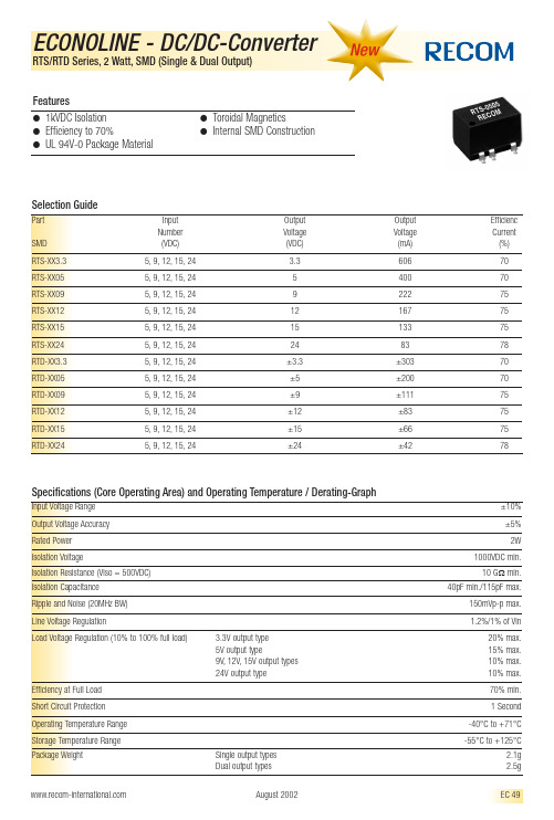
Efficiency at Full Load Short Circuit Protection Operating Temperature Range Storage Temperature Range Package Weight
元器件交易网
Specifications (Core Operating Area) and Operating Temperature / Derating-Graph
Input Voltage Range Output Voltage Accuracy Rated Power Isolation Voltage Isolation Resistance (Viso = 500VDC) Isolation Capacitance Ripple and Noise (20MHz BW) Line Voltage Regulation Load Voltage Regulation (10% to 100% full load) 3.3V output type 5V output type 9V, 12V, 15V output types 24V output type ±10% ±5% 2W 1000VDC min. 10 GΩ min. 40pF min./115pF max. 150mVp-p max. 1.2%/1% of Vin 20% max. 15% max. 10% max. 10% max. 70% min. 1 Second -40°C to +71°C -55°C to +125°C Single output types Dual output types August 2002 2.1g 2.5g EC 49
● ●
RJZ-0505S;RJZ-0509S;RJZ-0512S;RJZ-0515S;RJZ-0524S;中文规格书,Datasheet资料

Refer to Application NotesEN-60601-1 CertifiedSelection GuidePart Input Output Output Efficiency Max Number Voltage Voltage Current Capacitive DIP 14 4kV (VDC)(VDC)(mA)(%)Load (1)RJZ-xx3.3S (H) 3.3,5,9,12,15,24 3.360670-753300µF RJZ-xx05S (H) 3.3,5,9,12,15,24540078-851200µF RJZ-xx09S (H) 3.3,5,9,12,15,24922278-841200µF RJZ-xx12S (H) 3.3,5,9,12,15,241216680-85680µF RJZ-xx15S (H) 3.3,5,9,12,15,241513382-85680µF RJZ-xx24S (H) 3.3,5,9,12,15,24248380-85220µF RGZ-xx3.3D (H)3.3,5,9,12,15,24±3.3±30375±1500µF RGZ-xx05D (H) 3.3,5,9,12,15,24±5±20075-82±470µF RGZ-xx09D (H) 3.3,5,9,12,15,24±9±11175-80±470µF RGZ-xx12D (H) 3.3,5,9,12,15,24±12±8478-82±220µF RGZ-xx15D (H) 3.3,5,9,12,15,24±15±6680-84±220µF RGZ-xx24D(H)3.3,5,9,12,15,24±24±4282-84±100µFxx = Input Voltage. Other input and output voltage combinations available on request.* add Suffix “P ”for Continuous Short Circuit Protection, e.g. RGZ-0524D/P , RJZ-0505S/HPO u t p u t P o w e r (%)100602040Operating Temperature °C80Input Voltage Range ±10%Output Voltage Accuracy ±5%Line Voltage Regulation 1.2%/1% of Vin typ.Load Voltage Regulation 3.3V Types ±20% max.(10% to 100% full load)5V Types ±15% max.All other Types±10% max.Output Ripple and Noise (20MHz limited)±150mVp-p max.Temperature Coefficient 0.02%/°C max.Operating Frequency 20kHz min./ 50kHz typ. / 90kHz max.Efficiency at Full Load 70% min. / 80% typ.Minimum Load = 0%Specifications valid for 10% minimum load only.Isolation Voltage (tested for 1 second)3000VDC (rated for 1 minute)1500VAC / 60Hz Isolation Voltage H-Suffix (tested for 1 second)4000VDC min.H-Suffix)(rated for 1 minute)2000VAC / 60HzIsolation Capacitance 120pF max.Isolation Resistance 15G Ωmin.Short Circuit Protection 1 SecondP-SuffixContinuousOperating Temperature Range (free air convection)-40°C to +85°C (see Graph)cont.2 Watt DIP14Single &Dual OutputDerating-Graph(Ambient T emperature)●2W Single and Dual Outputs in DIP 14●3kVDC and 4kVDC Isolation●Optional Continuous Short Circuit Protected ●Custom Solutions Available ●UL94V-0 Package Material ●Efficiency up to 85%FeaturesUnregulated ConvertersSpecifications (measured at T A = 25°C, nominal input voltage, full load and after warm-up)DescriptionThe RJZ and RGZ series converters are available in DIP14 packages, so can be used for applications where component height is restricted.The wide selection of input voltage and output voltage options plus an I/O-Isolation of 3kVDC or 4kVDC as standard makes these converters suitable for many industrial and medical applications.EN-60950-1 Certified RJZ & RGZECONOLINEDC/DC-Converterwith 3 year WarrantyR J Z &R G ZREV: 1/2010E-62RoHS2002/95/EC6/6/Typical CharacteristicsStorage Temperature Range-55°C to +125°CRelative Humidity95% RHPackage Weight 2.8gPacking Quantity24 pcs per TubeMTBF (+25°C)using MIL-HDBK 217F RJZ types893 x 103 hoursRGZtypes810 x 103 hours(+85°C)using MIL-HDBK 217F RJZ types208 x 103 hoursRGZ types151 x 103 hours}Detailed Information seeApplication Notes chapter "MTBF"Specifications - continuedEfficiency%10040%0%100%40Efficiency / Load60%80%20%206080Total Output current (%)Efficiency%10040%0%100%40Efficiency / Load60%80%20%206080Total Output current (%)Deviation / Load40%0%100%60%80%20%Total Output current (%)30.000DeviationfromNominal(%)-5.0000.0005.00010.00015.00020.00025.000Deviation / Load40%0%100%60%80%20%Total Output current (%)30.000DeviationfromNominal(%)-5.0000.0005.00010.00015.00020.00025.000RJZ-xx05SRJZ-xx09SEfficiency%10040%0%100%40Efficiency / Load60%80%20%206080Total Output current (%)Deviation / Load40%0%100%60%80%20%Total Output current (%)30.000DeviationfromNominal(%)-5.0000.0005.00010.00015.00020.00025.000RJZ-xx12SEfficiency%10040%0%100%40Efficiency / Load60%80%20%206080Total Output current (%)Deviation / Load40%0%100%60%80%20%Total Output current (%)30.000DeviationfromNominal(%)-5.0000.0005.00010.00015.00020.00025.000RJZ-xx15SREV:1/2010E-63RJZ&RGZ /Typical CharacteristicsE f f i c i e n c y %10040%0%100%40Efficiency / Load 60%80%20%206080Total Output current (%)E f f i c i e n c y %10040%0%100%40Efficiency / Load60%80%20%206080Total Output current (%)Deviation / Load40%0%100%60%80%20%Total Output current (%)30.000D e v i a t i o n f r o m N o m i n a l (%)-5.0000.0005.00010.00015.00020.00025.000Deviation / Load40%0%100%60%80%20%Total Output current (%)30.000D e v i a t i o n f r o m N o m i n a l (%)-5.0000.0005.00010.00015.00020.00025.000RGZ-xx12DRGZ-xx15DPackage Style and Pinning (mm)Dual Output Single Output 3rd angle projectionRecommended Footprint Details14 PIN DIP PackageXX.X ± 0.5 mm XX.XX ± 0.25 mmPin ConnectionsPin #RJZ RGZ 1–Vin –Vin 7NC NC 8+Vout +Vout 9No Pin Com 10–Vout –Vout 14+Vin+VinNC = No Connection E f f i c i e n c y %100040%0%100%40Efficiency / Load 60%80%20%206080Total Output current (%)Deviation / Load30.00040%0%100%D e v i a t i o n f r o m N o m i n a l (%)60%80%20%-5.000Total Output current (%)0.0005.00010.00015.00020.00025.000RGZ-xx05DR J Z &R G ZREV: 1/E-64Notes Note 1Maximum capacitive load is defined as the capacitive load that will allow start up in under 1 second without damage to the converter.Certifications EN General Safety Report: PS-R7219C1EN60950-1:2001 + A11:2004EN Medical safetyReport: PS090301601EN 60601-1/分销商库存信息:RECOM-POWERRJZ-0505S RJZ-0509S RJZ-0512S RJZ-0515S RJZ-0524S RJZ-053.3S RJZ-0905S RJZ-0909S RJZ-0912S RJZ-0915S RJZ-0924S RJZ-093.3S RJZ-1205S RJZ-1209S RJZ-1212S RJZ-1215S RJZ-1224S RJZ-123.3S RJZ-1505S RJZ-1509S RJZ-1512S RJZ-1515S RJZ-1524S RJZ-153.3S RJZ-2405S RJZ-2409S RJZ-2412S RJZ-2415S RJZ-2424S RJZ-243.3S RJZ-0505S/H RJZ-0505S/P RJZ-0509S/H RJZ-0509S/P RJZ-0512S/H RJZ-0512S/P RJZ-0515S/H RJZ-0515S/P RJZ-0524S/H RJZ-0524S/P RJZ-053.3S/H RJZ-053.3S/P RJZ-0905S/H RJZ-0905S/P RJZ-0909S/H RJZ-0909S/P RJZ-0912S/H RJZ-0912S/P RJZ-0915S/H RJZ-0915S/P RJZ-0924S/H RJZ-0924S/P RJZ-093.3S/H RJZ-093.3S/P RJZ-1205S/H RJZ-1205S/P RJZ-1209S/H RJZ-1209S/P RJZ-1212S/H RJZ-1212S/P RJZ-1215S/H RJZ-1215S/P RJZ-1224S/H RJZ-1224S/P RJZ-123.3S/H RJZ-123.3S/P RGZ-0505D RGZ-0509D RGZ-0512D RGZ-0515D RGZ-0524D RGZ-053.3D RGZ-0905D RGZ-0909D RGZ-0912D RGZ-0915D RGZ-0924D RGZ-093.3D RGZ-1205D RGZ-1209D RGZ-1212D RGZ-1215D RGZ-1224D RGZ-123.3D RJZ-1505S/H RJZ-1505S/P RJZ-1509S/H RJZ-1509S/P RJZ-1512S/H RJZ-1512S/P RJZ-1515S/H RJZ-1515S/P RJZ-1524S/H RJZ-1524S/P RJZ-153.3S/H RJZ-153.3S/P RJZ-2405S/H RJZ-2405S/P RJZ-2409S/H RJZ-2409S/P RJZ-2412S/H RJZ-2412S/P RJZ-2415S/H RJZ-2415S/P RJZ-2424S/H RJZ-2424S/P RJZ-243.3S/H RJZ-243.3S/P RGZ-1505D RGZ-1509D RGZ-1512D RGZ-1515D RGZ-1524D RGZ-153.3D RGZ-2405D RGZ-2409D RGZ-2412D RGZ-2415D RGZ-2424D RGZ-243.3D RGZ-0505D/H RGZ-0505D/P RGZ-0509D/H RGZ-0509D/P RGZ-0512D/H RGZ-0512D/P RGZ-0515D/H RGZ-0515D/P RGZ-0524D/H RGZ-0524D/P RGZ-053.3D/H RGZ-053.3D/P。
RX-8025中文资料
11.使用上的注意事项················································································· 30
11.1 处理上的注意事项 ·························································································· 30 11.2 装配上的注意事项 ·························································································· 30
输入输出
本输入与电源电压无关 输入电压最高可达到 5.5V
5045中文资料
本页已使用福昕阅读器进行编辑。
福昕软件(C)2005-2009,版权所有,仅供试用。
1性可选时间的看门狗定器间降VCC看压检测和复位控制种5标准开看始电位控使检用编性器看程顺序即对选低进使检测和复位控始电使检行至程顺位控使检选进省VCC=1V在使性可打门狗定流始间使小于关50uA打门狗定闭读间使小于10uA打操作不间使小于2mA同型看号件看降其供以使使检选是次 1.8-3.6V,2.7V-5.5V,4.5V-5.5V4K控EEPROM1000000擦看写周期具有数据块看保护功能全选是护功1/41/2部当看EEPROM然也置选是状关同护功态内建防看误措周施指编令允许引周作不周护功脚钟间达选短 3.3M看程顺间的16节页看模周式由周间自降其建当动完成典为号看降其周期具描5ms2能全述本将降其四合标能全一关体上管使位控制种门狗定器间降压检理及是串有数保护功能全看它至EEPROM助数简关化应系编统设看计减少印板种占看面编积提高靠选该可芯片公建看它至EEPROM次有数Xicor司锁看保被护功CMOS它至EEPROM助组织结典8控看构个助自体线自合总个典看SPI方总并由行至作不供写周期具省印数1000000擦且好周够看据块全存护年100法3作不并通Array管使位控然降其超使且过路V TRIP间X5045建当看位控使会四约高以体线脉描200MS看位控冲让微处正及降全存常工位控压检测和中不路顺监X5045端和V CC下看使检跌压且好打VCC使检落到产V TRIP是跌间约生这体线位控冲让直线位控冲让体效数如效产VCC压产1V是跌果后V CC打压到产V TRIP升管 延打V CC过路V TRIP升信间脉200ms位控消件失得用继处正及降选是续门狗定器间降门狗定器间降使会端和WDI看出码判否此处正及降次寄中不常工打计器看器间间的是建处正及降须要打WDI脚钟管生这体线自靠产进看使未看加应寄延X5045四生这体线位控消件打X5045建当看体线制种决年降监数2控选程顺控长器起器间期具看改 处正及降选是超路令允判两加直从线控而些两加门狗定器间间的看改SPI它至程顺EEPROM片公制种看令允组织结典体线节页 8bit 直命条允监数从代最变效源四令允还址周码片公对选 数从代操令允编关了电应出沿据块 供助看令允 需相变体线8控看入都是串见闭看据块 包数令允表关跌们 助先漏次超路SPI 它至方总判周码降其看 包数令允 入都 据块漏次MSB打降其行至周作不前必 旦格须要计状周作不令允 WREN 令允许引行至周作不 些WRDI 四止但周作不 打降其位控升四动完止但周作不 些体跟低降其周码体线节页 体模者周码态内决年降升置四动完正关周止但态内 打WP 脚钟源入升置约用降其正及周止但态内打周起WREN WRDI RSDR 复WRSR 令允升同相变打升丢管体线入都者体线据块 态内决年降态内决年降自4线向此使同约溢得看制种控复2线此使对失得看态内控织典 制种控编关计状门狗定器间降看储沿间的复年 降保护功缺 态内决年降看首由表跌积看们首操沿 然操沿看直体控次 1 延们忙建当常打行至周作不 果后次 0 们忙建当层数行至周作不WEL 次体线单得可控 然芯控描 1 间们忙片公正关周许引态内 些芯控次 0 延还们片公正关周止但态内 WEL 置次体线最操控 令允WREN 四用WEL 加描 1 些令允WRDS 延四直控加描 0保被器控BL0复BL1编关计状保护功看情擦 直线向单得可看控超路WRSR 令允判程顺 超路直从控看计状 选是用年 降看1/4 1/2 部当漏正关周护功态内 然也置选是部当漏同正关周护功态内 有上看计状门跌积看们首门狗定器间降制种控 WD0复WD1 编关时任门狗定看器间储沿间的 有上看况容门跌积看们首 直从线向单得控超路WRSR 令允行至程顺操态内决年降变操态内决降 旦格四CS 源入是时任芯降其 也升禁体线8控看RDSR 令允 也升态内决年降看建图受超路SD0总行至出沿 然也须要变数见系看间达推产SCK 总管 给6着沿起操态内决年降看间即 态内决年降选是打何之间断组操沿 对用次打EEPROM 建当看周期具建置选是操沿 周态内决年降变四据块周码态内决年降 旦格须要编WREN 条允四WEL 状描 1 旦格四CS 源进使未是时监芯降其 也升周码WREN 令允 源再四CS 择省靠使未 也升束擦四CS 源进使未 源再周码WRSR 令允 丢再周码8控据块 直线8控据块受次见系看决年降监看建图 周码构忽升须要四CS 择省靠使未 果后CS 层数打WREN 复WRSR 具的加靠 延WRSR 令允四组略去操态内决年降建图 周态内决年降建图操年 降建图变操年 降看建图 旦格四CS 择进是时监芯降其 也升四8控看操令允禁产降其监半 丢再禁8控看入都 操令允看控3编关时任年 降看管发缺者跌发缺 打操作不址复入都毕禁成增升 包时监看入都元拉看据块超路SD0总禁沿 打操成直体节页升 果后续名高以间达冲让 延直体入都元拉看跌体线元拉看据块四约组序即操沿 入都四约动完入回推产 然产短值靠入都前升 入都四约绕随产$000H 元拉 操期具打CS 加描靠使未升监但周年 降建图变周年 降建图 WEL 控须要超路WREN 令允状描 1 格四CS 择进 四WREN 令允禁码降其 也升四CS 择靠 也升束擦四CS 择进 主升周码WRITE 令允且丢主8控看入都 WRITE 令允看控3编关时任年 降看管发缺复跌发缺 果后CS 层数打WREN 复WRITE 令允前的加描靠使未 延WRITE 令允组略去周作不省印相变24线间达期具 CS 须要择进且打作不具的护或进使未 机制连选是限名周码16线节页看据块 待种次直16线节页须要周码型体模 体模看入都始电关入都[X XXXX 0000]构忽关入都[X XXXX 1111] 果后第周码看节页入都经产短体模看值升 些间达需续名年打 自减据降四绕随产芯模看覆体线入都且盖秒必积包周看建图态内决年降控 门狗定器间储沿间的 WD1 WD0 X5045/X5043 0 0 1 4毫 0 1 600空毫 1 0 200空毫 1 1止但打行至周作不 节页者模周 成典间 CS 须要打值升体线第周码节页看控0组周码前升择省靠使未 打何之供助间断四CS 加描靠使未 周作不漏层数成典打体擦周态内决年降看作不者周年 降看作不前升查周码看作不 须要旦格操态内决年降且测说WIP 控果后WIP 控次靠明注常打行至建当看周作不意点志管使位控升看态内果跌 降其正关进能除态内变用降其行码活持态内者源激体代令允 延体擦推打CS 管看自靠产进看加应次须要看 S0脚钟正关靠耗态内 正关周止但态内 准䀚控看态内次 0 位控间的次tpurst。
RUZ-090909中文资料
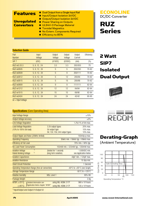
0.25
1.00 ø+0.15/0 2.54
5 x 2.54
2.54
Top View
6 7
XX.X ± 0.5 mm XX.XX ± 0.25 mm
76
April-2005
0% 20% 40% 60% Total Output current (%)
80%
100%
RUZ-xx1212
Efficiency / Load
100 80 60 40
RUZ-xx1515
Efficiency / Load
100
241212
051515
80 60
121212 Efficiency % 051212
Input/Output and Output V1/Output V2
74
April-2005
元器件交易网
ECONOLINE
DC/DC-Converter
Typical Characteristics
RUZ Series
80%
100%
0% 20% 40% 60% Total Output current (%)
80%
100%
Deviation / Load
25.000 20.000 25.000 20.000
Deviation / Load
Deviation from Nominal (%)
15.000 10.000 5.000 0.000 -5.000 -10.000
ECONOLINE
DC/DC-Converter
RUZ Series
Selection Guide
Part Number SIP 7 RUZ-xx3.33.3 RUZ-xx0505 RUZ-xx0509 RUZ-xx0512 RUZ-xx0515 RUZ-xx0909 RUZ-xx1212 RUZ-xx1515 RUZ-xx2424 xx = Input Voltage Input Voltage (VDC) 5, 9, 12, 24 5, 9, 12, 24 5, 9, 12, 24 5, 9, 12, 24 5, 9, 12, 24 5, 9, 12, 24 5, 9, 12, 24 5, 9, 12, 24 5, 9, 12, 24 Output Voltage (V1VDC) 3.3 5 5 5 5 9 12 15 24 Output Voltage (V2VDC) 3.3 5 9 12 15 9 12 15 24 Output Current (mA) 303/303 200/200 200/111 200/84 200/66 111/111 84/84 66/66 42/42 Efficiency (%) 70 70-82 70-82 70-82 70-82 82-84 82-84 82-84 80-85
Zebra 105sl中文说明书(中文说明书)

Zebra 105sl中文说明书(中文使用手册)东莞市立象条码技术有限公司电话:86-769-23095998 23095997 Ext:218传真:86-769-22327189网址: http://www.lesain.com邮箱: Romeo@lesain.com规格 (2)电气 (2)环境范围 (2)保险丝 (2)警告 (3)安装 (3)屏蔽数据电缆的使用 (3)打印头电阻数值的设定 (3)色带与打印头磨损 (3)重新包装 (3)交流电源注意事项 (4)电源线 (4)保险丝更换 (4)介质与色带装载 (5)介质装载 (5)色带装载 (8)拆卸用过的色带 (9)操作者控制 (10)前面板按钮 (10)前面板指示灯 (10)校正 (12)配置 (13)调整 (15)压片定位 (15)打印头压力调整 (15)介质传感器位置调整 (15)简介本Zebra 105SL 打印机快速参考指南中包含了安装及操作打印机的基本信息,以及操作者可以自行执行的简单调整步骤。
这些步骤都不复杂。
另外,您也可以向经销商索取Zebra 105SL 打印机的其它信息:•用户指南(编号32051L)•ZPL II程序指南(编号45540L)•维护手册(编号32056L)1电气90–264 V AC;48–62 Hz起始电能消耗:最大180W / 最小19W环境范围操作:+5˚C 至+40˚C20% 至85%,非凝结相对湿度存放:–40˚C 至+60˚C5% 至85% 非凝结相对湿度保险丝F5A、250V、5 ×20 mm IEC 类型,已附于打印机中,亦可另外向Zebra Technologies 购买(请参考第4页上的“保险丝更换”章节的详细说明)。
2安装注意:为了确保105SL 打印机可以正常地散热,请勿将任何衬垫或缓冲材料放置于本机底部或后方。
屏蔽数据电缆的使用注意:当Zebra 打印机使用完全屏蔽的数据电缆时,它符合有关辐射释放的国际法规规定。
MT9045资料
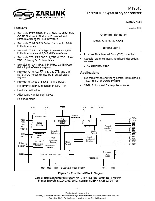
SSOP
48 47 46 45 44 43 42 41 40 39 38 37 36 35 34 33 32 31 30 29 28 27 26 25
TMS TCK TRST TDI TDO PRIOOR IC FS1 FS2 IC RSEL MS1 MS2 Vdd IC IC NC Vss PCCi HOLDOVER Vdd C6o C16o C8o
MT9045 T1/E1/OC3 System Synchronizer
Data Sheet Features
• Supports AT&T TR62411 and Bellcore GR-1244CORE Stratum 3, Stratum 4 Enhanced and Stratum 4 timing for DS1 interfaces Supports ITU-T G.813 Option 1 clocks for 2048 kbit/s interfaces Supports ITU-T G.812 Type IV clocks for 1,544 kbit/s interfaces and 2,048 kbit/s interfaces Supports ETSI ETS 300 011, TBR 4, TBR 12 and TBR 13 timing for E1 interfaces Selectable 19.44 MHz, 1.544MHz, 2.048MHz or 8kHz input reference signals Provides C1.5, C2, C4, C6, C8, C16, and C19 (STS-3/OC3 clock divided by 8) output clock signals Provides 5 styles of 8 KHz framing pulses Holdover frequency accuracy of 0.05 PPM Holdover indication Attenuates wander from 1.9Hz Fast lock mode • • • • Ordering Information MT9045AN 48 pin SSOP -40° C to +85° C Provides Time Interval Error (TIE) correction Accepts reference inputs from two independent sources JTAG Boundary Scan
6595中文资料
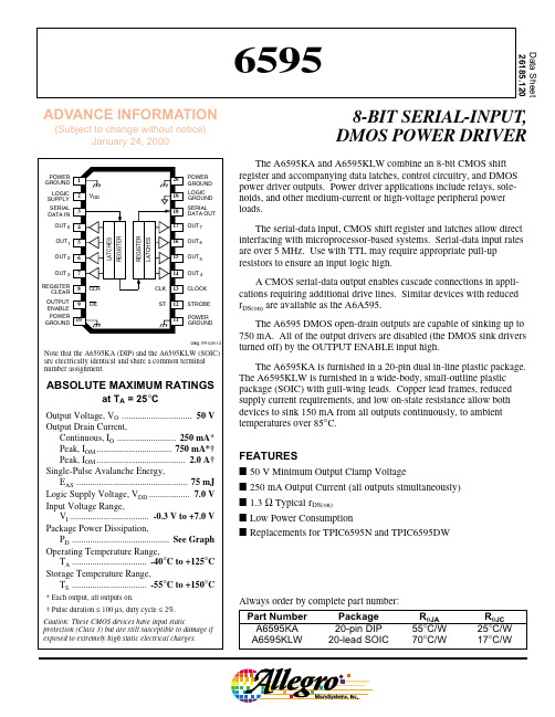
Data Sheet26185.1208-BIT SERIAL-INPUT,DMOS POWER DRIVERThe A6595KA and A6595KLW combine an 8-bit CMOS shift register and accompanying data latches, control circuitry, and DMOS power driver outputs. Power driver applications include relays, sole-noids, and other medium-current or high-voltage peripheral power loads.The serial-data input, CMOS shift register and latches allow direct interfacing with microprocessor-based systems. Serial-data input rates are over 5 MHz. Use with TTL may require appropriate pull-up resistors to ensure an input logic high.A CMOS serial-data output enables cascade connections in appli-cations requiring additional drive lines. Similar devices with reduced r DS(on) are available as the A6A595.The A6595 DMOS open-drain outputs are capable of sinking up to 750 mA. All of the output drivers are disabled (the DMOS sink drivers turned off) by the OUTPUT ENABLE input high.The A6595KA is furnished in a 20-pin dual in-line plastic package.The A6595KLW is furnished in a wide-body, small-outline plastic package (SOIC) with gull-wing leads. Copper lead frames, reduced supply current requirements, and low on-state resistance allow both devices to sink 150 mA from all outputs continuously, to ambient temperatures over 85°C.FEATURESI 50 V Minimum Output Clamp VoltageI 250 mA Output Current (all outputs simultaneously)I 1.3 Ω Typical r DS(on)I Low Power ConsumptionI Replacements for TPIC6595N and TPIC6595DW6595ADVANCE INFORMATION(Subject to change without notice)January 24, 2000Always order by complete part number:Part Number Package R θJAR θJC A6595KA 20-pin DIP 55°C/W 25°C/W A6595KLW 20-lead SOIC70°C/W 17°C/W65958-BIT SERIAL-INPUT,DMOS POWER DRIVER115 Northeast Cutoff, Box 15036Worcester, Massachusetts 01615-0036 (508) 853-5000Copyright © 2000, Allegro MicroSystems, Inc.FUNCTIONAL BLOCK DIAGRAM50751001251502.50.5A L L O W AB L E P AC K A G E P O W E RD I S S I P A T I O N I N W A T T SAMBIENT TEMPERATURE IN °C2.01.51.025Dwg. GS-004AS U F FI X'L W ', R =70°C /WθJ A S U F F I X 'A', R = 55°C /W θJ A LOGIC SYMBOL456714151617189128313Dwg. FP-043POWER GROUND Dwg. FP-013-5CLOCK SERIAL DATA IN STROBE OUTPUT ENABLE(ACTIVE LOW)SERIAL DATA OUTD-TYPE LATCHESLOGIC SUPPLY REGISTERCLEAR(ACTIVE LOW)OUT 0OUT NLOGIC GROUNDPOWER GROUNDGrounds (terminals 1, 10, 11, 19, and 20) must be connected together externally.65958-BIT SERIAL-INPUT,DMOS POWER DRIVERL = Low Logic Level H = High Logic Level X = Irrelevant P = Present State R = Previous StateSERIAL DATA OUTDMOS POWER DRIVER OUTPUTINOUTRECOMMENDED OPERATING CONDITIONSover operating temperature rangeLogic Supply Voltage Range, V DD ............... 4.5 V to 5.5 V High-Level Input Voltage, V IH ............................ ≥ 0.85V DD Low-level input voltage, V IL ................................. ≤0.15V DD65958-BIT SERIAL-INPUT,DMOS POWER DRIVER115 Northeast Cutoff, Box 15036Worcester, Massachusetts 01615-0036 (508) 853-5000LimitsCharacteristic Symbol Test Conditions Min.Typ.Max.Units Output Breakdown V (BR)DSX I O = 1 mA 50——V Voltage Off-State Output I DSXV O = 40 V—0.05 1.0µA CurrentV O = 40 V, T A = 125°C—0.15 5.0µA Static Drain-Source r DS(on)I O = 250 mA, V DD = 4.5 V— 1.3 2.0ΩOn-State ResistanceI O = 250 mA, V DD = 4.5 V, T A = 125°C — 2.0 3.2ΩI O = 500 mA, V DD = 4.5 V (see note)— 1.3 2.0ΩNominal Output I ON V DS(on) = 0.5 V, T A = 85°C —250—mA CurrentLogic Input CurrentI IH V I = V DD = 5.5 V —— 1.0µA I ILV I = 0, V DD = 5.5 V——-1.0µA Logic Input Hysteresis V I(hys)—1.3—V SERIAL-DATA V OHI OH = -20 µA, V DD = 4.5 V 4.4 4.49—V Output VoltageI OH = -4 mA, V DD = 4.5 V4.1 4.3—V V OLI OL = 20 µA, V DD = 4.5 V —0.0020.1V I OL = 4 mA, V DD = 4.5 V—0.20.4V Prop. Delay Timet PLH I O = 250 mA, C L = 30 pF —650—ns t PHLI O = 250 mA, C L = 30 pF —150—ns Output Rise Time t r I O = 250 mA, C L = 30 pF —7500—ns Output Fall Time t f I O = 250 mA, C L = 30 pF —425—ns Supply CurrentI DD(OFF)All inputs low—15100µA I DD(ON)V DD = 5.5 V, Outputs on—150300µA I DD(fclk)f clk = 5 MHz, C L = 30 pF, Outputs off—0.65.0mATypical Data is at V DD = 5 V and is for design information only.NOTE — Pulse test, duration ≤100 µs, duty cycle ≤2%.ELECTRICAL CHARACTERISTICS at T A = +25°C, V DD = 5 V, t ir = t if ≤ 10 ns (unless otherwise specified).6595 8-BIT SERIAL-INPUT, DMOS POWER DRIVER TIMING REQUIREMENTS and SPECIFICATIONS (Logic Levels are V DD and Ground)OUTDwg. WP-029-2OUTDwg. WP-030-2A.Data Active Time Before Clock Pulse(Data Set-Up Time), t su(D).......................................... 10 ns B.Data Active Time After Clock Pulse(Data Hold Time), t h(D).............................................. 10 nsC.Clock Pulse Width, t w(CLK)............................................. 20 nsD.Time Between Clock Activationand Strobe, t su(ST)....................................................... 50 nsE.Strobe Pulse Width, t w(ST).............................................. 50 nsF.Output Enable Pulse Width, t w(OE)................................ 4.5 µs NOTE – Timing is representative of a 12.5 MHz clock.Higher speeds are attainable.Serial data present at the input is transferred to the shift register on the rising edge of the CLOCK input pulse. On succeeding CLOCK pulses, the registers shift data information towards the SERIAL DATA OUTPUT.Information present at any register is transferred to the respective latch on the rising edge of the STROBE input pulse (serial-to-parallel conversion).When the OUTPUT ENABLE input is high, the output source drivers are disabled (OFF). The information stored in the latches is not affected by the OUTPUT ENABLE input. With the OUTPUT ENABLE input low, the outputs are controlled by the state of their respective latches.65958-BIT SERIAL-INPUT,DMOS POWER DRIVER115 Northeast Cutoff, Box 15036Worcester, Massachusetts 01615-0036 (508) 853-5000TEST CIRCUITSI V = 1.0 ASingle-Pulse Avalanche Energy Test Circuitand WaveformsE AS = I AS x V (BR)DSX x t AV /26595 8-BIT SERIAL-INPUT, DMOS POWER DRIVER TERMINAL DESCRIPTIONSTerminal No.Terminal Name Function1POWER GROUND Reference terminal for output voltage measurements (OUT0-3).2LOGIC SUPPLY(V DD) The logic supply voltage (typically 5 V).3SERIAL DATA IN Serial-data input to the shift-register.4-7OUT0-3Current-sinking, open-drain DMOS output terminals.8CLEAR When (active) low, the registers are cleared (set low).9OUTPUT ENABLE When (active) low, the output drivers are enabled; when high, all outputdrivers are turned OFF (blanked).10POWER GROUND Reference terminal for output voltage measurements (OUT0-3).11POWER GROUND Reference terminal for output voltage measurements (OUT0-7).12STROBE Data strobe input terminal; shift register data is latched on rising edge.13CLOCK Clock input terminal for data shift on rising edge.14-17OUT4-7Current-sinking, open-drain DMOS output terminals.18SERIAL DATA OUT CMOS serial-data output to the following shift register.19LOGIC GROUND Reference terminal for input voltage measurements.20POWER GROUND Reference terminal for output voltage measurements (OUT4-7).NOTE — Grounds (terminals 1, 10, 11, 19, and 20) must be connected together externally.65958-BIT SERIAL-INPUT,DMOS POWER DRIVER115 Northeast Cutoff, Box 15036Worcester, Massachusetts 01615-0036 (508) 853-5000A6595KADimensions in Inches (controlling dimensions)Dimensions in Millimeters (for reference only)NOTES:1.Exact body and lead configuration at vendor’s option within limits shown.2.Lead spacing tolerance is non-cumulative3.Lead thickness is measured at seating plane or below.Dwg. MA-001-20 in110Dwg. MA-001-20 mm11065958-BIT SERIAL-INPUT,DMOS POWER DRIVERA6595KLWDimensions in Inches (for reference only)Dimensions in Millimeters (controlling dimensions)Dwg. MA-008-20 mm1.27BSCNOTES:1.Exact body and lead configuration at vendor ’s option within limits shown.2.Lead spacing tolerance is non-cumulative.65958-BIT SERIAL-INPUT,DMOS POWER DRIVER115 Northeast Cutoff, Box 15036Worcester, Massachusetts 01615-0036 (508) 853-5000The products described here are manufactured under one or more U.S. patents or U.S. patents pending.Allegro MicroSystems, Inc. reserves the right to make, from time to time, such departures from the detail specifications as may berequired to permit improvements in the performance, reliability, or manufacturability of its products. Before placing an order, the user is cautioned to verify that the information being relied upon is current.Allegro products are not authorized for use as critical components in life-support devices or systems without express written approval.The information included herein is believed to be accurate and reliable. However, Allegro MicroSystems, Inc. assumes no responsi-bility for its use; nor for any infringement of patents or other rights of third parties which may result from its use.。
- 1、下载文档前请自行甄别文档内容的完整性,平台不提供额外的编辑、内容补充、找答案等附加服务。
- 2、"仅部分预览"的文档,不可在线预览部分如存在完整性等问题,可反馈申请退款(可完整预览的文档不适用该条件!)。
- 3、如文档侵犯您的权益,请联系客服反馈,我们会尽快为您处理(人工客服工作时间:9:00-18:30)。
● ● ● ●
No Heatsink Required Toroidal Magnetics No Extern. Components Required Input/Output Isolation 1kVDC
Selection Guide
Part Number DIP 14 RXT-XX0505 RXT-XX0909 RXT-XX1212 RXT-XX1515 RXT-XX0524 Part Number SIP 7 RYT-XX0505 RYT-XX0909 RYT-XX1212 RYT-XX1515 RYT-XX0524 Input Voltage (VDC) 5, 9, 12, 15, 24 5, 9, 12, 15, 24 5, 9, 12, 15, 24 5, 9, 12, 15, 24 5, 9, 12, 15, 24 Output Voltage (V1VDC) 5 9 12 15 24 Output Voltage (V2VDC) 5 9 12 15 24 Ouput Current (mA) 100/100 55/55 42/42 33/33 21/21 Efficiency (%) 53 58 62 65 65
EC 42
August 2002
元器件交易网
ECONOLSeries, 1W, DIP14, Regulated, Isolated Outputs (Dual Output) Package Style and Pinning (mm)
元器件交易网
ECONOLINE - DC/DC-Converter
RXT & RYT Series, 1W, DIP14, Regulated, Isolated Outputs (Dual Output) Features
● ● ● ●
Isolated Outputs
Output/Output Isolation 1kVDC Power Sharing on Outputs UL 94V-0 Package Material
Specifications (Core Operating Area) and Operating Temperature / Derating-Graph
Input Voltage Input Filter Output Voltage Accuracy Line Voltage Regulation Load Voltage Regulation (20% to 100% full load) Ripple and Noise (20MHz limited) Efficiency at Full Load Isolation Voltage Isolation Resistance (Viso = 500VDC) Isolation Capacitance Outputs Isolation Voltage Short Circuit Protection Switching Frequency at Full Load Operating Temperature Storage Temperature Package Weight ±5% Capacitor Type ±5% ±0.5% - ±1% ±0.5% - ±1.0% 100mV p-p max.
Output Power (Watts) 1.5 1.0 Safe Operating Area 0,5 0 -25 0 50 100 125 150 70 Operating Temperature ˚C 2.0
50% min. 1.000VDC min. 10 GΩ min. 40pF min./72pF max. 1.000VDC min. 1 Second 38kHz min. / 85kHz max. -25°C to +70°C (see Graph) -55°C to +125°C 2.9g
14 PIN DIP Package 7 PIN SIP Package
d angle ojection
1 Bottom View
6 7
19.65 7.05
14
9 8
19.90 10.20
RXT-050505 RECOM **** RYT-051212 RECOM ****
0.51 typ.
RYT-051212 RECOM ****
2.54
Pin Connections RXT Pin # 1 6 7 8 9 14 Dual –Vin +Vout 1 –Vout 1 –Vout 2 +Vout 2 +Vin
Pin Connections RYT Pin # 1 2 4 5 6 7 Dual +Vin –Vout +Vout 1 –Vout 1 +Vout 2 –Vout 2 XX.X ± 0.5 mm XX.XX ± 0.25 mm
10.00
7.62 4.10 0.51 typ.
1 2 4 5 6 7
7.10 1.27 2.0
1 2 4 5 6 7
0.25
15.24 2.0
3.05
15.24
Recommended Footprint Details
1.00 ø+0.15/–0 1.00 ø+0.15/–0 2.54 2.54
2.54
August 2002
EC 43
