MT8808中文资料
模拟开关矩阵MT8808的性能及其应用
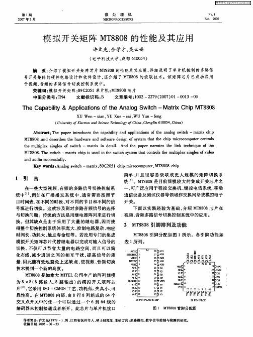
2 M 80 T 8 8引脚排 列及功能
M 80 T 88引脚 分配 如 图 1所 示 。各 引脚 功 能如
模拟开关矩阵芯片代替继电器以完成对输入信号的 . 表 1 列 。 所 切换 , 仅可 以节 省 大量 的 电路 空 间 , 不 而且 可 以简 A Y2 — 弋
AYI
n u o s c e sul a d a di A a o w th —mar 8 C 0 1 c i c o o u e ; 8 0 h p y wo d : n l g s i c t x; 9 2 5 h p mir c mp tr MT 8 8 c i i
化布线 , 减少通道之 间的相 互干扰 , 提高信号 的质 量, 因此 能有效 地避 免 上 述 缺 点 , 视 频 、 频 切换 使 音
技 术提 到一个新 的高 度 。
 ̄ ”X E3 2 2 E 6 q 9 口 8 A 肿
a 譬蓦 l l毛鏊 叠毫 星 毫叠
M 80 是加拿大 M T L T 88 IE 公司生产 的阵列规模 为 8×8( 8路 输 入 , 8路 输 出 ) 的模 拟 开 关 矩 阵 芯 片 J它 采用 IO—C S工 艺 , , S MO 功耗 低 、 失真 小 、 可
维普资讯
第 1期 20 0 7年 2月
微
处
理
机
No 1 .
MI CR0P R0CE S S ORS
F b. 2 0 e .0 7
模 拟 开关 矩 阵 M 80 T 8 8的性 能及 其 应 用
许文先 , 学才 , 余 吴云峰
( 电子科技 大学 , 成都 6 0 5 ) 10 4
摘 要: 介绍 了 模拟开关矩阵芯片 M 80 T 88的性能及其应用 , 详细说 明了单片机控制的多路信 号开关矩阵的硬件电路设计和软件设计, 还介绍 了 M 80 T 88的级联技术。该矩 阵芯片 已成功应用
8808说明书

产品概述Tenda 系列10M 以太网集线器为您提供最为便捷、最为经济的小型网络平台。
只需使用通用的网络电缆(双绞线)将各个网络设备与我们的集线器端口相连接,即可接入网络。
您可以通过前面板的LED 指示灯状态查看每个端口的连接状态,非常方便您观察网络情况。
集线器还具备UPLINK 端口,便于和其它网络设备之间级联,适用于您对网络的扩展。
主要特性1. 遵循IEEE802.3 10BASE-T 以太网标准2. 5/8个10Mbps 端口3. 前面板LED 工作状态指示灯4. 塑胶壳迷你桌面型5. 一个Uplink 端口方便扩展网络6. 外接式电源7. 即插即用LED 指示灯集线器的指示灯包括Power、Link/Rx 指示。
指示灯用于设备监控和故障显示。
下面对每个指示灯做出解释。
LED指示灯颜色状态描述 绿色亮 集线器已接通电源 Power— 灭 集线器未通电 绿色亮 端口正常连接到网络 绿色闪烁端口正在通信 Link/Rx— 灭 端口未连接到网络技术指标一般特性标准 IEEE802.3 10BASE-T以太网标准 协议 CSMA/CD数据传输率以太网:10Mbps(半双工)拓扑结构 星型网络电缆 非屏蔽双绞线(UTP) 3,4,5类 最大长度:100米EIA/TIA-568 100欧姆屏蔽双绞线(STP) 最大长度:100米端口数量 5/8个10Mbps端口物理及环境特性AC输入 180-240VAC,50/60Hz AC输出 9V 500mA运行温度 0°C~65°C存储温度 0°C~80°C湿度 5%~90%无凝结EMI FCC Class A,CE Mark Class A,VCCI Class A,BSMI Class A安装方法安装集线器分下列几步:z至少可负重3Kg的表面。
z电源插座与设备应在1.5米以内。
z认真检查电源,核实完全安全连接。
z确认在设备周围,有足够的通风口,可以很好的扩散热量。
论文-电话自动录音控制电路的设计

电话自动录音控制电路的设计摘 要:自动录音电话机是自动应答和自动录音相结合的电话机,当有电话呼叫自动录音电话机时,若主人不在,电话机可自动启动,播放存储器中的留言,然后启动录音装置,记录对方留言。
录音结束方式是自动识别电话线路忙音信号后停录并自动挂机。
主人回来后可按放音键收听对方留言。
本电话自动录音系统,利用AT89C51控制外围电路和语音芯片ISD4004,实现振铃检测、自动摘挂机、忙音检测、自动录放音等功能。
可以直接通过按键控制录放音,同时使用音频处理电路把语音信号传送到电话线上去或者录制到语音芯片中。
关键词:电话 自动录音 ISD4004正文1 引言本设计利用单片机控制外围电路和语音芯片,来完成基于单片机的电话自动录音系统的设计与功能实现。
其功能包括:振铃检测、自动摘挂机、自动录放音、忙音检测等。
系统框图入下:图1-1 系统原理框图 本设计采用AT89C51系列单片机作为系统的控制单元本方案的控制部分。
当有电话进来,振铃检测电路检测到振铃信号通过P0.0送给单片机。
每来一个信号单片机就记1次数,振铃检测电路单片机 录音电路 语音芯片 放音电路摘挂机电路忙音检测电路当满3次后判断为无人接听并把单片机的P1.0口置高电平,RL1继电器线圈得电吸合将市话外线摘机。
摘机后单片机通过P1.4,P1.5对ISD4004的MISO,MOSI读写状态字和命令字来控制ISD4004的录音和放音。
如果在录音过程检测到忙音信号表明对方已挂机,把单片机的P1.0口置低电平使RL1继电器断电,摘挂机电路断路实现挂机。
在本设计中,采用ISD4004语音芯片,ISD4004为美国ISD公司出品的优质单片语音录放电路,由振荡器、语音存储单元、前置放大器、自动增益控制电路、抗干扰滤波器、输出放大器组成。
一个最小的录放系统仅由一个麦克风、一个喇叭、两个按钮、一个电源、少数电阻电容组成。
录音内容存入永久存储单元,提供零功率信息存储,这个独一无二的方法是借助于美国ISD公司的专利--直接模拟存储技术(DAST、TM)实现的。
SmartAX MT880d 快速入门(V100R001_01,路由,国内版)
项目 标准
规格 ADSL 标准
ADSL2 标准 ADSL2+标准
ITU G.992.1(G.dmt)Annex A ITU G.994.1(G.hs) ANSI T1.413 Issue 2 ITU G.992.3(G.dmt.bis)Annex A ITU G.992.5 Annex A
如果您的计算机使用的操作系统是 Windows XP,您可以使用 Windows XP 自带 的 PPP 拨号程序。在 Windows XP 操作系统中创建拨号连接的操作步骤如下:
1. 单击“开始 > 所有程序 > 附件 > 通讯 > 网络连接”菜单项。 2. 在“网络任务”栏,单击“创建一个新的连接”,弹出“新建连接向
话线等,以免设备遭雷击损坏。 z 请使用产品配套的附件以及厂商推荐的配件,例如电源适配器等。 z 设备供电电压必须满足设备的输入电压要求。 z 在存储、运输和使用设备的过程中,必须严格保持干燥。 z 请将设备安放在通风、无强光直射的环境中。 z 安放设备时请远离热源或裸露的火源,例如电暖器、蜡烛等。安放设备时请
指示灯 POWER
状态 常亮 不亮
含义 MT880d 通电。 MT880d 未通电。
4
指示灯 ADSL LAN
DATA
状态 闪烁 常亮 不亮 闪烁 常亮 不亮 闪烁 不亮
含义 MT880d 正在激活。 MT880d 已激活。 MT880d 未接通电源。 以太网接口有数据流量。 以太网接口已经建立连接。
步骤 3 检查终端“LAN”指示灯是否点亮。
如果“LAN”指示灯不亮,请参考下面的说明进行检查。
1. 请检查计算机网卡是否已经启用。 2. 请检查终端和计算机之间的网线连接是否牢靠。请尝试重新插拔
Atmel AT88SC0808CA 密码存储芯片数据手册说明书
AT88SC0808CAAtmel CryptoMemorySUMMARY DATASHEETFeatures ∙ One of a family of devices with user memories from 1-Kbit to 8-Kbits ∙8-Kbit (1-Kbyte) EEPROM user memory∙ Eight 1-Kbit (128-byte) zones ∙ Self-timed write cycle∙ Single byte or 16-byte page write mode ∙ Programmable access rights for each zone∙ 2-Kbit configuration zone∙ 37-byte OTP (One-Time Programmable) area for user-defined codes ∙ 160-byte area for user-defined keys and passwords ∙High security features∙ 64-bit mutual authentication protocol (under license of ELVA) ∙ Cryptographic Message Authentication Codes (MAC) ∙ Stream encryption∙ Four key sets for authentication and encryption ∙ Eight sets of two 24-bit passwords ∙ Anti-tearing function∙ Voltage and frequency monitors∙Smart card features∙ ISO 7816 Class B (3V) operation∙ ISO 7816-3 asynchronous T=0 Protocol (Gemplus ®Patent) * ∙ Multiple zones, key sets and passwords for multi-application use ∙ Synchronous 2-wire serial interface for faster device initialization * ∙ Programmable 8-byte answer-to-reset register (ATR) ∙ISO 7816-2 compliant modules∙Embedded application features∙ Low voltage supply: 2.7V – 3.6V∙ Secure nonvolatile storage for sensitive system or user information ∙ 2-wire serial interface (TWI, 5V compatible) ∙ 1.0MHz compatibility for fast operation∙ Standard 8-lead plastic packages, green compliant (exceeds RoHS)∙Same pin configuration as Atmel ®AT24CXXX Serial EEPROM in SOIC and PDIP packages∙High reliability∙ Endurance: 100,000 cycles ∙ Data retention: 10 years ∙ ESD protection: 2,000V min* Note: Modules available with either T=0 / 2-wire modes or 2-wire mode onlyThis is a summary document. The complete document is available on the Atmel website at .AT88SC0808CA [Summary DATASHEET]Atmel-5204IS-CryptoMem-AT88SC0808CA-Datasheet-Summary_0720152Table 1. Pin AssignmentsPin Configuration123487658-lead SOIC, PDIPNC NCNC GNDV CCNC SCL SDA8-lead TSSOPNCV CC 81NC C N 72NCK L C 63GND 54SDA 12348765SDA GND CLK V CC8-lead Ultra Thin Mini-MAP (MLP 2x3)Bottom ViewNCNC NC NC TWI Smart Card ModuleV C C =C1 NC =C2 SCL/CLK=C3NC=C4C5=GND C6=NC C7=S D A /IO C8=NCISO Smart Card ModuleV C C =C1 RST=C2 SCL/CLK=C3NC=C4C5=GND C6=NC C7=S D A /IO C8=NCAT88SC0808CA [Summary DATASHEET]Atmel-5204IS-CryptoMem-AT88SC0808CA-Datasheet-Summary_07201531. DescriptionThe Atmel AT88SC0808CA member of the Atmel CryptoMemory ®family is a high-performance secure memory providing 8-Kbit of user memory with advanced security and cryptographic features built in. The user memory is divided into eight128-byte zones, each of which may be individually set with different security access rights or effectively combined together to provide space for one to eight data files. The AT88SC0808CA features an enhanced command set that allows directcommunication with microcontroller hardware 2-wire interface thereby allowing for faster firmware development with reduced code space requirements.1.1 Smart Card ApplicationsThe AT88SC0808CA provides high security, low cost, and ease of implementation without the need for a microprocessor operating system. The embedded cryptographic engine provides for dynamic, symmetric-mutual authentication between the device and host, as well as performing stream encryption for all data and passwords exchanged between the device and host. Up to four unique key sets may be used for these operations. The AT88SC0808CA offers the ability to communicate with virtually any smart card reader using the asynchronous T = 0 protocol (Gemplus Patent) defined in ISO 7816-3.1.2 Embedded ApplicationsThrough dynamic, symmetric-mutual authentication, data encryption, and the use of cryptographic Message Authentication Codes (MAC), the AT88SC0808CA provides a secure place for storage of sensitive information within a system. With its tamper detection circuits, this information remains safe even under attack. A 2-wire serial interface running at speeds up to 1.0MHz provides fast and efficient communications with up to 15 individually addressable devices. The AT88SC0808CA is available in industry standard 8-lead packages with the same familiar pin configuration as Atmel AT24CXXX Serial EEPROM devices. Note:Does not apply to either the TSSOP or the Ultra Thin Mini-Map pinoutsFigure 1-1. Block DiagramV CC GNDSCL/CLK SDA/IORSTAT88SC0808CA [Summary DATASHEET]Atmel-5204IS-CryptoMem-AT88SC0808CA-Datasheet-Summary_07201542. Connection DiagramFigure 2-1. Connection Diagram3.Pin Descriptions3.1Supply Voltage (V CC )The V CC input is a 2.7V to 3.6V positive voltage supplied by the host.3.2 Clock (SCL/CLK)When using the asynchronous T = 0 protocol, the CLK (SCL) input provides the device with a carrier frequency f . The nominal length of one bit emitted on I/O is defined as an “elementary time unit” (ETU) and is equal to 372/ f .When using the synchronous protocol, data clocking is done on the positive edge of the clock when writing to the device and on the negative edge of the clock when reading from the device.3.3 Reset (RST)The AT88SC0808CA provides an ISO 7816-3 compliant asynchronous answer-to-reset (ATR) sequence. Upon activation of the reset sequence, the device outputs bytes contained in the 64-bit ATR register. An internal pull-up on the RST input pad allows the device to operate in synchronous mode without bonding RST. The AT88SC0808CA does not support an ATR sequence in the synchronous mode of operation.3.4 Serial Data (SDA/IO)The SDA/IO pin is bidirectional for serial data transfer. This pin is open-drain driven and may be wired with any number of other open-drain or open-collector devices. An external pull-up resistor should be connected between SDA/IO and V CC . The value of this resistor and the system capacitance loading the SDA/IO bus will determine the rise time of SDA/IO. This rise time will determine the maximum frequency during read operations. Low value pull-up resistors will allow higher frequency operations while drawing higher average power supply current. SDA/IO information applies to both asynchronous andsynchronous protocols.AT88SC0808CA [Summary DATASHEET]Atmel-5204IS-CryptoMem-AT88SC0808CA-Datasheet-Summary_07201554. Absolute Maximum Ratings**Notice:Stresses beyond those listed under “AbsoluteMaximum Ratings” may cause permanent damage to the device. This is a stress rating only and functional operation of the device at these or any other condition beyond those indicated in the operational sections of this specification is not implied. Exposure to absolute maximum rating conditions for extended periods of time may affect device reliability.Table 4-1.DC CharacteristicsApplicable over recommended operating range from V CC = +2.7 to 3.6V, T AC = -40°C to +85°C (unless otherwise noted)Note:1. To prevent latch up conditions from occurring during power up of the AT88SC0808CA, V CC must be turned onbefore applying V IH . For powering down, V IH must be removed before turning V CC off.AT88SC0808CA [Summary DATASHEET]Atmel-5204IS-CryptoMem-AT88SC0808CA-Datasheet-Summary_0720156Table 4-2.AC CharacteristicsApplicable over recommended operating range from V CC = +2.7 to 3.6V, T AC = -40°C to +85°C, CL = 30pF (unless otherwise noted)5.Device Operations for Synchronous Protocols5.1Clock and Data TransitionsThe SDA pin is normally pulled high with an external device. Data on the SDA pin may change only during SCL low time periods (see Figure 5-3 on page 8). Data changes during SCL high periods will indicate a start or stop condition as defined below.5.1.1 Start conditionA high-to-low transition of SDA with SCL high defines a start condition which must precede all commands (see Figure 5-4 on page 8).5.1.2 Stop conditionA low-to-high transition of SDA with SCL high defines a stop condition. After a read sequence, the stop condition will place the EEPROM in a standby power mode (see Figure 5-4 on page 8).5.1.3 AcknowledgeAll addresses and data words are serially transmitted to and from the EEPROM in 8-bit words. The EEPROM sends a zero to acknowledge that it has received each word. This happens during the ninth clock cycle (see Figure 5-5 on page 8).AT88SC0808CA [Summary DATASHEET]Atmel-5204IS-CryptoMem-AT88SC0808CA-Datasheet-Summary_07201575.2 Memory ResetAfter an interruption in communication due protocol errors, power loss or any reason, perform "Acknowledge Polling" to properly recover from the condition. Acknowledge polling consists of sending a start condition followed by a valid CryptoMemory command byte and determining if the device responded with an acknowledge. Figure 5-1. Bus Time for 2-wire Serial CommunicationsSCL: Serial Clock, SDA: Serial Data I/OFigure 5-2. Write Cycle TimingSCL: Serial Clock, SDA: Serial Data I/ONote:The write cycle time t WR is the time from a valid stop condition of a write sequence to the end of the internal clear/write cycleSCLSDA INSDA OUTAT88SC0808CA [Summary DATASHEET]Atmel-5204IS-CryptoMem-AT88SC0808CA-Datasheet-Summary_0720158Figure 5-3. Data ValidityFigure 5-4. START and STOP DefinitionsFigure 5-5. Output AcknowledgeST ARTACKNOWLEDGESCLDAT A INDAT A OUT189AT88SC0808CA [Summary DATASHEET]Atmel-5204IS-CryptoMem-AT88SC0808CA-Datasheet-Summary_07201596.Device Architecture6.1User ZonesThe EEPROM user memory is divided into eight zones of 1-Kbit each. Multiple zones allow for storage of different types of data or files in different zones. Access to user zones is permitted only after meeting proper security requirements. These security requirements are user definable in the configuration memory during device personalization. If the same security requirements are selected for multiple zones, then these zones may effectively be accessed as one larger zone. Figure 6-1. User Zones7. Control LogicAccess to the user zones occur only through the control logic built into the device. This logic is configurable through access registers, key registers and keys programmed into the configuration memory during device personalization. Also implemented in the control logic is a cryptographic engine for performing the various higher-level security functions of the device.AT88SC0808CA [Summary DATASHEET]Atmel-5204IS-CryptoMem-AT88SC0808CA-Datasheet-Summary_072015108. Configuration MemoryThe configuration memory consists of 2048 bits of EEPROM memory used for storage of passwords, keys, codes, and also used for definition of security access rights for the user zones. Access rights to the configuration memory are defined in the control logic and are not alterable by the user after completion of personalization. Figure 8-1. Configuration Memory9. Security FusesThere are three fuses on the device that must be blown during the device personalization process. Each fuse locks certain portions of the configuration zone as OTP (One-Time Programmable) memory. Fuses are designed for the modulemanufacturer, card manufacturer and card issuer and should be blown in sequence, although all programming of the device and blowing of the fuses may be performed at one final step.10. Communication Security ModesCommunications between the device and host operate in three basic modes. Standard mode is the default mode for thedevice after power-up. Authentication mode is activated by a successful authentication sequence. Encryption mode isactivated by a successful encryption activation following a successful authentication.Table 10-1. Communication Security Modes(1)Note: 1. Configuration data include viewable areas of the configuration zone except the passwords:•MDC: Modification Detection Code•MAC: Message Authentication Code11. Security Options11.1 Anti-TearingIn the event of a power loss during a write cycle, the integrity of the device’s stored data is recoverable. This function isoptional: the host may choose to activate the anti-tearing function, depending on application requirements. When anti-tearing is active, write commands take longer to execute, since more write cycles are required to complete them, and data is limited toa maximum of eight bytes for each write request.Data is written first into a buffer zone in EEPROM instead of the intended destination address, but with the same accessconditions. The data is then written in the required location. If this second write cycle is interrupted due to a power loss, the device will automatically recover the data from the system buffer zone at the next power-up. Non-volatile buffering of the data is done automatically by the device.During power-up in applications using anti-tearing, the host is required to perform ACK polling in the event that the deviceneeds to carry out the data recovery process.11.2 Write LockIf a user zone is configured in the write lock mode, the lowest address byte of an 8-byte page constitutes a write access byte for the bytes of that page.Example: The write lock byte at $080 controls the bytes from $081 to $087Figure 11-1. Write Lock ExampleThe write lock byte itself may be locked by writing its least significant (rightmost) bit to “0”. Moreover, when write lock mode is activated, the write lock byte can only be programmed – that is, bits written to “0” cannot return to “1”.In the write lock configuration, write operations are limited to writing only one byte at a time. Attempts to write more than one byte will result in writing of just the first byte into the device.11.3 Password VerificationPasswords may be used to protect read and/or write access of any user zone. When a valid password is presented, it ismemorized and active until power is turned off, unless a new password is presented or RST becomes active. There are eight password sets that may be used to protect any user zone. Only one password is active at a time. Presenting the correct write password also grants read access privileges.11.4 Authentication ProtocolThe access to a user zone may be protected by an authentication protocol. Any one of four keys may be selected to use with a user zone.Authentication success is memorized and active as long as the chip is powered, unless a new authentication is initialized or RST becomes active. If the new authentication request is not validated, the card loses its previous authentication which must be presented again to gain access. Only the latest request is memorized. Figure 11-2. Password and Authentication OperationsNote:Authentication and password verification may be attempted at any time and in any order. Exceedingcorresponding authentication or password attempts trial limit renders subsequent authentication or password verification attempts futile.READ ACCESSWRITE ACCESS11.5 Cryptographic Message Authentication CodesAT88SC0808CA implements a data validity check function in the standard, authentication or encryption modes of operation.In the standard mode, data validity check is done through a Modification Detection Code (MDC), in which the host may read an MDC from the device in order to verify that the data sent was received correctly.In authentication and encryption modes, the data validity check becomes more powerful since it provides a bidirectional data integrity check and data origin authentication capability in the form of a Message Authentication Codes (MAC). Only thehost/device that carried out a valid authentication is capable of computing a valid MAC. While operating in the authentication or encryption modes, the use of MAC is required. For an ingoing command, if the device calculates a MAC different from the MAC transmitted by the host, not only is the command abandoned but the security privilege is revoked. A new authentication and/or encryption activation will be required to reactivate the MAC.11.6 EncryptionThe data exchanged between the device and the host during read, write and verify password commands may be encrypted to ensure data confidentiality.The issuer may choose to require encryption for a user zone by settings made in the configuration memory. Any one of four keys may be selected for use with a user zone. In this case, activation of the encryption mode is required in order to read/write data in the zone and only encrypted data will be transmitted. Even if not required, the host may still elect to activate encryption provided the proper keys are known.11.7 Supervisor ModeEnabling this feature allows the holder of one specific password to gain full access to all eight password sets, including the ability to change passwords.11.8 Modify ForbiddenNo write access is allowed in a user zone protected with this feature at any time. The user zone must be written during device personalization prior to blowing the security fuses.11.9 Program OnlyFor a user zones protected by this feature, data can only be programmed (bits change from a “1” to a “0”), but not erased (bi ts change from a “0” to a “1”).12. Protocol SelectionThe AT88SC0808CA supports two different communication protocols.∙ Smartcard Applications:Smartcard applications use ISO 7816-B protocol in asynchronous T = 0 mode for compatibility and interoperability with industry standard smartcard readers.∙ Embedded Applications:A 2-wire serial interface provides fast and efficient connectivity with other logic devices or microcontrollers.The power-up sequence determines establishes the communication protocol for use within that power cycle. Protocol selection is allowed only during power-up.12.1 Synchronous 2-wire Serial InterfaceThe synchronous mode is the default mode after power up. This is due to the presence of an internal pull-up on RST. For embedded applications using CryptoMemory in standard plastic packages, this is the only available communication protocol.∙ Power-up V CC , RST goes high also∙ After stable V CC , SCL(CLK) and SDA(I/O) may be driven∙ Once synchronous mode has been selected, it is not possible to switch to asynchronous mode without first poweringoff the deviceFigure 12-1. Synchronous 2-wire ProtocolNote: Five clock pulses must be sent before the first command is issued.V cc I/O-SDARST CLK-SCL1234512.2 Asynchronous T = 0 ProtocolThis power-up sequence complies to ISO 7816-3 for a cold reset in smart card applications.∙ V CC goes high; RST, I/O (SDA) and CLK (SCL) are low ∙ Set I/O (SDA) in receive mode ∙ Provide a clock signal to CLK (SCL) ∙RST goes high after 400 clock cyclesThe device will respond with a 64-bit ATR code, including historical bytes to indicate the memory density within the CryptoMemory family.Once asynchronous mode has been selected, it is not possible to switch to synchronous mode without first powering off the device.Figure 12-2. Asynchronous T = 0 Protocol (Gemplus Patent)13. Initial Device ProgrammingEnabling the security features of CryptoMemory requires prior personalization. Personalization entails setting up of desired access rights by zones, passwords and key values, programming these values into the configuration memory with verification using simple write and read commands, and then blowing fuses to lock this information in place.Gaining access to the configuration memory requires successful presentation of a secure (or transport) code. The initial signature of the secure (transport) code for the AT88SC0808CA device is $22 E8 3F. This is the same as the Write 7 password. The user may elect to change the signature of the secure code anytime after successful presentation.After writing and verifying data in the configuration memory, the security fuses must be blown to lock this information in the device. For additional information on personalizing CryptoMemory, please see the application notes ProgrammingCryptoMemory for Embedded Applications and Initializing CryptoMemory for Smart Card Applications from the product page at /products/securemem .V cc I/O-SDARSTCLK-SCL14. Ordering InformationNote: 1. Formal drawings may be obtained from an Atmel sales office.2. Both the J and P module packages are used for either ISO (T=0 / 2-wire mode) or TWI (2-wire mode only).15. Package InformationOrdering Code: MJ or MJTG Ordering Code: MP or MPTGModule Size: M2Dimension*: 12.6 x 11.4 [mm] Glob Top: Round - ∅8.5 [mm] Thickness: 0.58 [mm]Pitch: 14.25mm Module Size: M2Dimension*: 12.6 x 11.4 [mm]Glob Top: Square - 8.8 x 8.8 [mm] Thickness: 0.58 [mm]Pitch: 14.25mmNote: *The module dimensions listed refer to the dimensions of the exposed metal contact area. The actual dimensions of the module after excise or punching from the carrier tape are generally 0.4mm greater in both directions(i.e., a punched M2 module will yield 13.0 x 11.8mm).15.1 Atmel AT88SC0808CA Package Marking Information15.2 Ordering Code: SH8S1 – 8-lead JEDEC SOIC15.3 Ordering Code: PU8P3 – 8-lead PDIPAT88SC0808CA [Summary DATASHEET]Atmel-5204IS-CryptoMem-AT88SC0808CA-Datasheet-Summary_0720152115.4Ordering Code: TH 8X – 8-lead TSSOPAT88SC0808CA [Summary DATASHEET]Atmel-5204IS-CryptoMem-AT88SC0808CA-Datasheet-Summary_0720152215.5Ordering Code: Y6H-T8MA2 – 8-lead Ultra Thin Mini-MapAT88SC0808CA [Summary DATASHEET]Atmel-5204IS-CryptoMem-AT88SC0808CA-Datasheet-Summary_0720152316. Revision History。
华为smartAX MT880的路由功能设置图文介绍
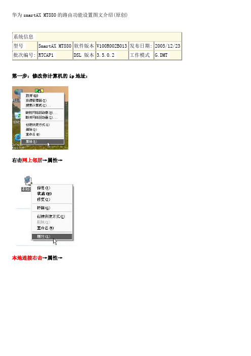
华为smartAX MT880的路由功能设置图文介绍(原创)
第一步:修改你计算机的ip地址:
右击网上邻居→属性→
本地连接右击→属性→
Internet 协议 (TCP/IP)→属性→
设置成:IP地址192.168.1.2,子网掩码为255.255.255.0→默认网关为192.168.1.1(DNS根据当地的电信和网通的实际地址来输入或192.168.1.1(我的网通DNS:202.102.134.68、202.102.128.68))
第二步:
在IE浏览器地址栏中输入192.168.1.1
密码和帐号均为Admin
第三步:
点击ATM设置(在左侧面)→
模式选择Routing→
VPI为0→VCI为35(网通是33)→启用为Yes→协议为PPPoE→封装格式LLC→服务商名称“ADSL”→输入自己的用户名和密码→默认路由“允许”→
其他默认→点击应用→OK!
第四步:
点击系统重启→ 当前设置→重启。
好了!你现在不用拨号也可以上网了。
中兴SR8808核心路由器SR02SRP2E3单板手册说明书

资料版本: T1-08231X-20071109-C-1.01 BOM: 3123A11XSR02SRP2E3单板手册1 单板标识前面板上标有丝印:SR02SRP2E3。
2 单板简介交换路由板,适用于SR8805/SR8808/SR8812核心路由器。
z单板规格表1SR02SRP2E3单板规格属性规格CPU MPC7447AFlash 64MBBootROM 1MBSDRAM 1GB(缺省),2GB(可选)CF卡 256MB(缺省),1GB(可选)单板尺寸(W×D) 366.7mm×340mm对外接口1个Console口,支持路由器的本地配置管理1个AUX口,支持路由器的远程拨号配置管理1个网管口:支持10/100/1000BASE-T接口1个RS232/485口,RS485支持级联。
1个CF卡插槽2个SMB同轴三级时钟输出接口2个SMB同轴三级时钟输入接口2个USB接口最大功耗135Wz面板及指示灯面板和指示灯如下图所示。
查询SR8808供应商捷多邦,专业PCB打样工厂,24小时加急出货资料版本: T1-08231X-20071109-C-1.01 BOM: 3123A11X(7)(8)(1)(9)(10)(11)(4)(5)(6)(3)(2)(1): SMB同轴时钟接口 (2):CF卡接口(3): CF卡状态指示灯(CFS) (4):10/100/1000BASE-T接口(5): USB接口 (6):RS232/485口(7): Console口 (8):AUX口(9): 系统复位键 (10):业务处理板状态指示灯(11): SR02SRP2E3状态指示灯Figure 1 SR02SRP2E3面板示意图说明:各接口及指示灯的详细说明请参见“产品安装手册”。
单板指示灯含义参见下表。
表2SR02SRP2E3单板指示灯说明指示灯状态含义灯亮表示交换网处于工作状态SFS灯灭表示交换网处于备用状态灯常亮表示单板有故障灯常灭表示单板有故障RUN(绿)灯闪烁表示单板正常工作灯灭表示单板无告警ALM(红)灯亮表示单板有告警灯亮表示该单板为主用ACT(绿)灯灭表示该单板为备用常亮表示CF卡在位,CF卡处于操作空闲状态,CF卡不能热插拔。
MT8801规格书-中文_Rev1.00
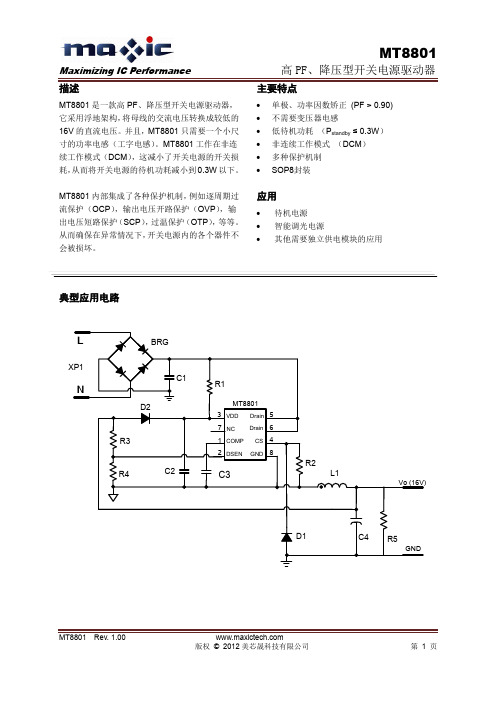
芯片标记:
MT8801 YY WW xxxx
生产内部代码 生产周代码 生产年代码
管脚描述
Name Pin No.
COMP
1
DSEN
2
VDD
3
CS
4
DRAIN 5,6
NC
7
GND
8
Description 内部误差放大器的输出引脚。用一个电容将其与地串联实现频率补偿。 输出电压的反馈引脚。 供给电压引脚。 内部 MOSFET 的源极,同时用来检测源极电流。 内部 MOSFET 的漏极。 无连接。 芯片地。
应用
待机电源 智能调光电源 其他需要独立供电模块的应用
典型应用电路
L
XP1
N
BRG
C1 D2
R3
R4
C2
R1
MT8801 3 VDD Drain 5 7 NC Drain 6 1 COMP CS 4 2 DSEN GND 8
C3
R2 L1
Vo (16V)
D1
C4 R5
GND
MT8801 Rev. 1.00
第6页
Maximizing IC Performance
MT8801
高 PF、降压型开关电源驱动器
索取产品详细信息及样片申请,请联系:
美芯晟科技有限公司 (北京办公室) 北京市海淀区知春路 106 号,皇冠假日酒店写字楼 1006。邮政编码 100086 电话: 86-10-62662828 传真: 86-10-62662951
版权 © 2012 美芯晟科技有限公司
第1页
Maximizing IC Performance 极限参数
VDD 引脚电压 Drain 引脚电压 COMP/CS/DSEN 引脚电压 焊接温度 (10 秒) 存储温度
MEMORY存储芯片MT29F8G08ABACAWP-ITC中文规格书
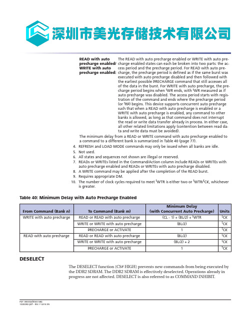
READ with auto precharge enabled/ WRITE with auto precharge enabled:The READ with auto precharge enabled or WRITE with auto pre-charge enabled states can each be broken into two parts: the ac-cess period and the precharge period. For READ with auto pre-charge, the precharge period is defined as if the same burst was executed with auto precharge disabled and then followed with the earliest possible PRECHARGE command that still accesses all of the data in the burst. For WRITE with auto precharge, the pre-charge period begins when t WR ends, with t WR measured as if auto precharge was disabled. The access period starts with regis-tration of the command and ends where the precharge period (or t RP) begins. This device supports concurrent auto precharge such that when a READ with auto precharge is enabled or a WRITE with auto precharge is enabled, any command to other banks is allowed, as long as that command does not interrupt the read or write data transfer already in process. In either case, all other related limitations apply (contention between read da-ta and write data must be avoided).The minimum delay from a READ or WRITE command with auto precharge enabled toa command to a different bank is summarized in Table 40 (page 77).4.REFRESH and LOAD MODE commands may only be issued when all banks are idle.5.Not used.6.All states and sequences not shown are illegal or reserved.7.READs or WRITEs listed in the Command/Action column include READs or WRITEs withauto precharge enabled and READs or WRITEs with auto precharge disabled.8. A WRITE command may be applied after the completion of the READ burst.9.Requires appropriate DM.10.The number of clock cycles required to meet t WTR is either two or t WTR/t CK, whicheveris greater.Table 40: Minimum Delay with Auto Precharge EnabledDESELECTThe DESELECT function (CS# HIGH) prevents new commands from being executed bythe DDR2 SDRAM. The DDR2 SDRAM is effectively deselected. Operations already inprogress are not affected. DESELECT is also referred to as COMMAND INHIBIT.Table 44: Truth Table – CKENotes: 1.CKE (n) is the logic state of CKE at clock edge n; CKE (n - 1) was the state of CKE at theprevious clock edge.2.Current state is the state of the DDR2 SDRAM immediately prior to clock edge n.mand (n) is the command registered at clock edge n, and action (n) is a result ofcommand (n).4.The state of ODT does not affect the states described in this table. The ODT function isnot available during self refresh (see ODT Timing (page 130) for more details and spe-cific restrictions).5.Power-down modes do not perform any REFRESH operations. The duration of power-down mode is therefore limited by the refresh requirements.6.“X” means “Don’t Care” (including floating around V REF) in self refresh and power-down. However, ODT must be driven high or low in power-down if the ODT function isenabled via EMR.7.All states and sequences not shown are illegal or reserved unless explicitly describedelsewhere in this document.8.Valid commands for power-down entry and exit are NOP and DESELECT only.9.On self refresh exit, DESELECT or NOP commands must be issued on every clock edge oc-curring during the t XSNR period. READ commands may be issued only after t XSRD (200clocks) is satisfied.10.Valid commands for self refresh exit are NOP and DESELECT only.11.Power-down and self refresh can not be entered while READ or WRITE operations,LOAD MODE operations, or PRECHARGE operations are in progress. See SELF REFRESH(page 118) and SELF REFRESH (page 79) for a list of detailed restrictions.12.Minimum CKE high time is t CKE = 3 × t CK. Minimum CKE LOW time is t CKE = 3 × t CK.This requires a minimum of 3 clock cycles of registration.13.Self refresh mode can only be entered from the all banks idle state.14.Must be a legal command, as defined in Table 37 (page 73).Figure 71: READ-to-Power-Down or Self Refresh EntryCKCK#CommandDQDQS, DQS#Don’t CareTransitioning DataAddressA10CKE Power-down or self refresh entryNotes:1.In the example shown, READ burst completes at T5; earliest power-down or self refreshentry is at T6.2.Power-down or self refresh entry may occur after the READ burst completes.Figure 72: READ with Auto Precharge-to-Power-Down or Self Refresh EntryCKCK#CommandDQDQS, DQS#Don’t CareTransitioning DataAddressA10CKEPower-down or self refresh 2 entry Notes:1.In the example shown, READ burst completes at T5; earliest power-down or self refreshentry is at T6.2.Power-down or self refresh entry may occur after the READ burst completes.ODT TimingOnce a 12ns delay (t MOD) has been satisfied, and after the ODT function has been ena-bled via the EMR LOAD MODE command, ODT can be accessed under two timing cate-gories. ODT will operate either in synchronous mode or asynchronous mode, depend-ing on the state of CKE. ODT can switch anytime except during self refresh mode and afew clocks after being enabled via EMR, as shown in Figure 81 (page 131).There are two timing categories for ODT—turn-on and turn-off. During active mode(CKE HIGH) and fast-exit power-down mode (any row of any bank open, CKE LOW,MR[12 = 0]), t AOND, t AON, t AOFD, and t AOF timing parameters are applied, as shown inFigure 83 (page 132).During slow-exit power-down mode (any row of any bank open, CKE LOW, MR[12] = 1)and precharge power-down mode (all banks/rows precharged and idle, CKE LOW),t AONPD and t AOFPD timing parameters are applied, as shown in Figure 84 (page 133).ODT turn-off timing, prior to entering any power-down mode, is determined by the pa-rameter t ANPD (MIN), as shown in Figure 85 (page 133). At state T2, the ODT HIGH sig-nal satisfies t ANPD (MIN) prior to entering power-down mode at T5. When t ANPD(MIN) is satisfied, t AOFD and t AOF timing parameters apply. Figure 85 (page 133) alsoshows the example where t ANPD (MIN) is not satisfied because ODT HIGH does not oc-cur until state T3. When t ANPD (MIN) is not satisfied, t AOFPD timing parameters apply.ODT turn-on timing prior to entering any power-down mode is determined by the pa-rameter t ANPD, as shown in Figure 86 (page 134). At state T2, the ODT HIGH signal sat-isfies t ANPD (MIN) prior to entering power-down mode at T5. When t ANPD (MIN) issatisfied, t AOND and t AON timing parameters apply. Figure 86 (page 134) also showsthe example where t ANPD (MIN) is not satisfied because ODT HIGH does not occur un-til state T3. When t ANPD (MIN) is not satisfied, t AONPD timing parameters apply.ODT turn-off timing after exiting any power-down mode is determined by the parame-ter t AXPD (MIN), as shown in Figure 87 (page 135). At state Ta1, the ODT LOW signalsatisfies t AXPD (MIN) after exiting power-down mode at state T1. When t AXPD (MIN) issatisfied, t AOFD and t AOF timing parameters apply. Figure 87 (page 135) also shows theexample where t AXPD (MIN) is not satisfied because ODT LOW occurs at state Ta0.When t AXPD (MIN) is not satisfied, t AOFPD timing parameters apply.ODT turn-on timing after exiting either slow-exit power-down mode or precharge pow-er-down mode is determined by the parameter t AXPD (MIN), as shown in Figure 88(page 136). At state Ta1, the ODT HIGH signal satisfies t AXPD (MIN) after exiting pow-er-down mode at state T1. When t AXPD (MIN) is satisfied, t AOND and t AON timing pa-rameters apply. Figure 88 (page 136) also shows the example where t AXPD (MIN) is notsatisfied because ODT HIGH occurs at state Ta0. When t AXPD (MIN) is not satisfied,t AONPD timing parameters apply.。
FLUKE 8808A Digtal Multimeter 说明书

®8808ADigtal Multimeter用户手册July 2007, Rev. 1, 12/09 (Simplified Chinese)© 2007, 2009 Fluke Corporation. All rights reserved. Specifications subject to change without notice.All product names are trademarks of their respective companies.有限保证和有限责任每台Fluke的产品在正常使用和维护的情况下保证没有材料和工艺上的缺陷。
产品的保证期为一年,从发运之日起计算。
零件、产品修理和维护的保证期为90天。
此项保证的对象仅为原始购买者或者Fluke授权代理商的最终使用客户,并且不适用于保险丝、普通电池或者Fluke认为由于意外的或不正常的工作或管理状况而错误使用、经过改动、疏忽管理、受到污染或损坏的产品。
Fluke保证软件将按照其功能技术指标牢靠地工作90天,并已经正确地记录在无缺陷的介质上。
Fluke不保证软件没有错误或工作中无中断。
Fluke授权代理商应当只将此种对新的和未使用过的产品的保证延伸到最终使用客户,但无权代表Fluke 做出更高的或不同的保证条件。
只有从Fluke授权的销售渠道购买的产品或者当购买者已经支付了适当的国际价格时才能获得这种保证支持。
当从一个国家购买的产品送到另一个国家进行修理时,Fluke保留向购买者开具发票收取修理/更换零件进口费用的权利。
Fluke的保证责任是有限的,对于在保证期之内退回到Fluke授权的维修中心的有缺陷的产品, Fluke可以选择退还购买款项、免费修理或更换产品。
为获得保修,请与您最近的Fluke授权维修中心联系以得到返修授权信息。
然后将该产品发送到该维修中心,提供故障说明、并付邮资和保险费(FOB目的地)。
MEMORY存储芯片MT29F64G08CBAAAWP-IT中文规格书

DQ12 VDDQ
VSS
UDQS# DQ14 VSSQ
UDQS DQ10 VDDQ
DQ8 VSSQ
VDD
LDM VSSQ VDDQ
DQ1 DQ3 VSSQ
VDD
VSS
VSSQ
DQ7 DQ5 VDDQ
CK
ห้องสมุดไป่ตู้VSS
NC
CK# VDD CKE
A10/AP ZQ
NC
NC VREFCA VSS
A12/BC# BA1 VDD
Symbol A[15:13], A12/BC#, A11, A10/AP, A[9:0]
BA[2:0] CK, CK#
CKE
CS# DM ODT RAS#, CAS#, WE# RESET#
Type Input
Input Input Input
Input Input Input Input Input
09005aef85af8fa8 4Gb_DDR3L.pdf - Rev. R 09/18 EN
4Gb: x4, x8, x16 DDR3L SDRAM Ball Assignments and Descriptions
Table 3: 78-Ball FBGA – x4, x8 Ball Descriptions
Clock enable: CKE enables (registered HIGH) and disables (registered LOW) internal circuitry and clocks on the DRAM. The specific circuitry that is enabled/ disabled is dependent upon the DDR3 SDRAM configuration and operating mode. Taking CKE LOW provides PRECHARGE POWER-DOWN and SELF REFRESH operations (all banks idle), or active power-down (row active in any bank). CKE is synchronous for power-down entry and exit and for self refresh entry. CKE is asynchronous for self refresh exit. Input buffers (excluding CK, CK#, CKE, RESET#, and ODT) are disabled during POWER-DOWN. Input buffers (excluding CKE and RESET#) are disabled during SELF REFRESH. CKE is referenced to VREFCA.
MF8808-PDF规格书

(VDD =5V, Gain=20dB, RL =8Ω, T =25°C, unless otherwise noted.)
Symbol Parameter
Test Conditions
THD+N=10%,f=1KHZ,RL=4Ω
VDD=5.0V VDD=3.6V
VDD=5.0V
THD+N=1%,f=1KHZ,RL=4Ω
VDD
2.5
5.5
V
2
VDD=5.0V
2
V
4
0.6
VDD=5.0V
0.6
V
0.6
热阻参数
Parameter
热阻(Junction to Ambient)
Symbol
θJA
Package
SOP16
MAX
115
UNIT
°C/W
Rev 1.0 May.2015
3 / 10
MF8808 3W 立体声 F 类音频功率放大器
Vos
失调电压
VIN=0V, VDD=5V
Fosc
工作频率
Tst
启动时间
Bypass capacitor =1uF
OTP OTH
温度保护 -
No Load, Junction Temperature
VDD=5.0V
MIN
2.5
TYP
3 1.55 2.5 1.3 1.72 0.9 1.45 0.75 0.05 0.07 0.03
MAX UNIT
W W W W % % dB dB
85
dB
80
μV 100
90
dB
200 mW
90
AO8808中文资料
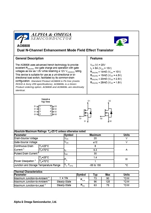
SymbolTyp Max 739096125R θJL 6375°C/W Maximum Junction-to-Ambient A Steady-State °C/W Maximum Junction-to-Lead CSteady-State°C/WThermal Characteristics ParameterUnits Maximum Junction-to-Ambient A t ≤ 10s R θJA AO8808AO8808SymbolMin TypMaxUnits BV DSS 20V 10T J =55°C25I GSS 100nA V GS(th)0.50.751V I D(ON)30A 10.614T J =125°C14.21712.215m Ω16.120m Ω23.228m Ωg FS 36S V SD 0.731V I S2.4A C iss 1810pF C oss 232pF C rss 200pF R g1.6ΩQ g 19.8nC Q gs 1.8nC Q gd 5nC t D(on) 3.3ns t r 5.9ns t D(off)44ns t f 7.7ns t rr 22ns Q rr9.8nCTHIS PRODUCT HAS BEEN DESIGNED AND QUALIFIED FOR THE CONSUMER MARKET. APPLICATIONS OR USES AS CRITICAL COMPONENTS IN LIFE SUPPORT DEVICES OR SYSTEMS ARE NOT AUTHORIZED. AOS DOES NOT ASSUME ANY LIABILITY ARISING OUT OF SUCH APPLICATIONS OR USES OF ITS PRODUCTS. AOS RESERVES THE RIGHT TO IMPROVE PRODUCT DESIGN,FUNCTIONS AND RELIABILITY WITHOUT NOTICE.I F =8A, dI/dt=100A/µs V GS =0V, V DS =10V, f=1MHz SWITCHING PARAMETERS Total Gate Charge V GS =4.5V, V DS =10V, I D =8AGate Source Charge Gate Drain Charge Gate resistanceV GS =0V, V DS =0V, f=1MHzTurn-Off Fall TimeTurn-On DelayTime V DS =5V, I D =8ADYNAMIC PARAMETERS Maximum Body-Diode Continuous CurrentInput Capacitance Output Capacitance Turn-On Rise Time Turn-Off DelayTime V GS =10V, V DS =10V, R L =1.3Ω, R GEN =3Ωm ΩV GS =4.5V, I D =5A I S =1A,V GS =0V V GS =1.8V, I D =3AForward TransconductanceDiode Forward Voltage Static Drain-Source On-ResistanceR DS(ON)I DSS µA Gate Threshold Voltage V DS =V GS I D =250µA V DS =16V, V GS =0VV DS =0V, V GS =±12V Zero Gate Voltage Drain Current Gate-Body leakage current Electrical Characteristics (T J =25°C unless otherwise noted)STATIC PARAMETERS ParameterConditions Body Diode Reverse Recovery Time Body Diode Reverse Recovery ChargeI F =8A, dI/dt=100A/µsDrain-Source Breakdown Voltage On state drain currentI D =250µA, V GS =0V V GS =2.5V, I D =4A V GS =4.5V, V DS =5V V GS =10V, I D =8AReverse Transfer Capacitance A: The value of R θJA is measured with the device mounted on 1in 2 FR-4 board with 2oz. Copper, in a still air environment with T A =25°C. The value in any given application depends on the user's specific board design. The current rating is based on the t ≤ 10s thermal resistance rating.B: Repetitive rating, pulse width limited by junction temperature.C. The R θJA is the sum of the thermal impedence from junction to lead R θJL and lead to ambient.D. The static characteristics in Figures 1 to 6,12,14 are obtained using 80 µs pulses, duty cycle 0.5% max.E. These tests are performed with the device mounted on 1 in 2FR-4 board with 2oz. Copper, in a still air environment with T A =25°C. The SOA curve provides a single pulse rating. Rev3: August 2005AO8808。
MT8880使用心得
MT8880使用心得2007年05月19日星期六 21:21MT8880是我们应用电话拨号应用中常用的一款芯片,它集发送、接收于一体。
如果设计得法还是一款相当稳定的IC,优点是:通过少量的几个元件就可以组成拨号及接收的电路。
唯一的缺点:我认为还是其价格,一片要30元左右。
对市场上价格竞争激烈的产品一般很少用到这款芯片。
双音多频(DTMF) 信号是由一级低音频信号和一组高音频信号,按一定的组合而构成的。
每组音频信号各有4 个音频信号,而每种组合有一个高频信号和一个低频信号,总共有16 种组合。
目前市场上DTMF 接收器和发生器大多是独立制造的,而在实际应用中同时需要DTMF 信号的收发功能,因此我们就希望有一种芯片能集DTMF 信号的收发功能于一体,这样就可以简化设计,降低成本,减少体积。
MT8880 就是一个带有呼叫处理滤波器(call progress filter) 的单片DTMF 收发器。
它的特点是:集成度高;数据传送稳定,抗干扰强;具有多种工作模式,可编程控制,容易与微机接口。
DTMF 技术早期主要应用在程控交换、移动通信, 近年来的研究发现它在远程控制、过程控制等自动控制领域方面,有着广阔的应用和发展前景。
外部的电话线和MT8880不以直接相连,要通过隔离才能间接连接,一般隔离可以通过隔离线圈或整流桥来解决,相对来讲我更喜欢一个桥来担当。
MT8880是一款双音频的语音拨号芯片。
它通用二个音频信号形成一位的数据信号发出去,一组为低频的、一是高频的信号。
接收的对方把二个音频信号分别接收下来一查表就知道收到的是哪个数据了。
通过表可知,发送1时为0001,发送2时发送0010......依次类推。
呵呵你要看清楚了,电话号码中的0可不能发送0000啊,第一次我就犯过这样的错误怎么有的电话可以拨通有的电话就是不通,通多个电话号码的一对比发现了号码中有0的电话号码都不通这才想到查一下表这才明白原来0对应1010,晕呐。
FLUKE 8808A 5.5 Digit Multimeter 数据手册
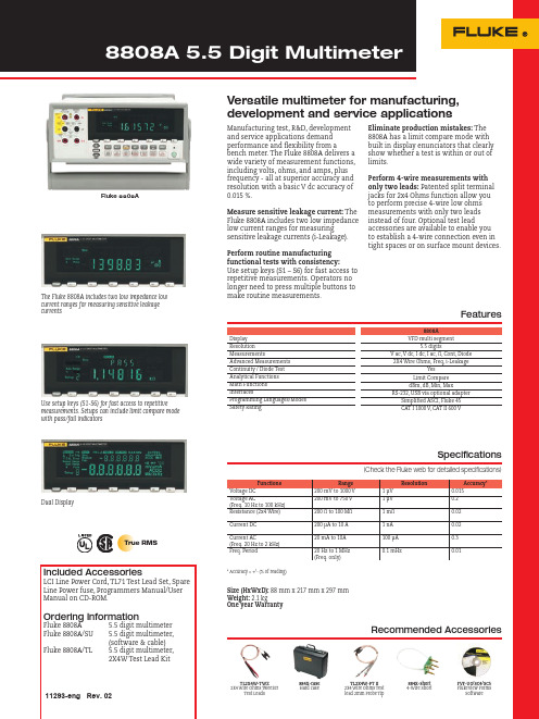
Dual Display
True RMS
Included Accessories
LCI Line Power Cord, TL71 Test Lead Set, Spare Line Power fuse, Programmers Manual/User Manual on CD-ROM.
Ordering Information
Eliminate production mistakes: The 8808A has a limit compare mode with built in display enunciators that clearly show whether a test is within or out of limits.
8808A VFD multi segment
5.5 digits V ac, V dc, I dc, I ac, Ω, Cont, Diode
2X4 Wire Ohms, Freq, i-Leakage Yes
Limit Compare dBm, dB, Min, Max RS-232, USB via optional adapter Simplified ASCI, Fluke 45 CAT I 1000 V, CAT II 600 V
Perform routine manufacturing functional tests with consistency: Use setup keys (S1 – S6) for fast access to repetitive measurements. Operators no longer need to press multiple buttons to make routine measurements.
- 1、下载文档前请自行甄别文档内容的完整性,平台不提供额外的编辑、内容补充、找答案等附加服务。
- 2、"仅部分预览"的文档,不可在线预览部分如存在完整性等问题,可反馈申请退款(可完整预览的文档不适用该条件!)。
- 3、如文档侵犯您的权益,请联系客服反馈,我们会尽快为您处理(人工客服工作时间:9:00-18:30)。
3-15®MT88088x 8Analog Switch ArrayFeatures•Internal control latches and address decoder •Short set-up and hold times•Wide operating voltage: 4.5V to 13.2V •12Vpp analog signal capability •R ON 65Ω max. @ V DD =12V, 25°C •∆R ON ≤ 10Ω @ V DD =12V, 25°C •Full CMOS switch for low distortion •Minimum feedthrough and crosstalk•Separate analog and digital reference supplies •Low power consumption ISO-CMOS technologyApplications•Key systems •PBX systems •Mobile radio•Test equipment /instrumentation •Analog/digital multiplexers •Audio/Video switchingDescriptionThe Mitel MT8808 is fabricated in MITEL’s ISO-CMOS technology providing low power dissipation and high reliability. The device contains a 8 x 8 array of crosspoint switches along with a 6 to 64 line decoder and latch circuits. Any one of the 64switches can be addressed by selecting the appropriate six address bits. The selected switch can be turned on or off by applying a logical one or zero to the DATA input. V SS is the ground reference of the digital inputs. The range of the analog signal is from V DD to V EE .Ordering InformationMT8808AC 28 Pin Ceramic DIP MT8808AE 28 Pin Plastic DIP MT8808AP 28 Pin PLCC-40° to 85°CFigure 1 - Functional Block Diagram6 to 64DecoderLatches8 x 8Switch ArrayAX0AX1AY0AY1AY2STROBE DATA RESET VDD VEE VSSXi I/O (i=0-7)Yi I/O (i=0-7)116464• • • • • • • • • • • • • • • • • • •• • • • • • • • • • • • • • • •AX2ISSUE 2November 1988ISO-CMOS 元器件交易网MT8808ISO-CMOS3-16Figure 2 - Pin ConnectionsPin DescriptionPin #Name Description1AY2AY2 Address Line (Input).2STROBE STROBE (Input): enables function selected by address and data. Address must be stablebefore STROBE goes high and DATA must be stable on the falling edge of the STROBE. Active High.3V EE Negative Power Supply.4DATA DATA (Input): a logic high input will turn on the selected switch and a logic low will turn off the selected switch. Active High.5V SS Digital Ground Reference .6-9X0, X2,X4, X6X0, X2, X4 and X6 Analog (Inputs/Outputs): these are connected to the X0, X2, X4 and X6 rows of the switch array.10RESET Master RESET (Input): this is used to turn off all switches. Active High.11-18Y7 - Y0Y7 - Y0 Analog (Inputs/Outputs): these are connected to the Y0 - Y7 columns of the switch array.19V DD Positive Power Supply.20-23X7, X5,X3, X1X7, X5, X3 and X1 Analog (Inputs/Outputs): these are connected to the X7, X5, X3 and X1 rows of the switch array.24-26AX0-AX2AX0 - AX2 Address Lines (Inputs).27,28AY0, AY1 AY0 and AY1 Address Lines (Inputs).12345678910111213141516171819202827262524232221AY2STROBEVEE DATA VSS X0X2X4X6RESETY7Y6Y5Y4AY1AY0AX2AX1AX0X1X3X5X7VDD Y0Y1Y2Y328 PIN CERDIP/PLASTIC DIP456789101125242322212019•D A T A AX1AX0X1X3X5X7VDDVSS X0X2X4X6RESETY7Y 132128272612131415161718V E E S T R O B E A Y 2A Y 1A Y 0A X 2Y 6Y 5Y 4Y 3Y 2Y 028 PIN PLCC元器件交易网ISO-CMOSMT88083-17Functional DescriptionThe MT8808 is an analog switch matrix with an array size of 8 x 8. The switch array is arranged such that there are 8 columns by 8 rows. The columns are referred to as the Y inputs/outputs and the rows are the X inputs/outputs. The crosspoint analog switch array will interconnect any X I/O with any Y I/O when turned on and provide a high degree of isolation when turned off. The control memory consists of a 64bit write only RAM in which the bits are selected by the address inputs (AY0-AY2, AX0-AX2). Data is presented to the memory on the DATA input. Data is asynchro-nously written into memory whenever the STROBE input is high and is latched on the falling edge of STROBE. A logical “1” written into a memory cell turns the corresponding crosspoint switch on and a logical “0” turns the crosspoint off. Only the crosspoint switches corresponding to the addressed memory location are altered when data is written into memory. The remaining switches retain their previous states. Any combination of X and Y inputs/outputs can be interconnected by establishing appropriate patterns in the control memory. A logical “1” on the RESET input will asynchronously return all memory locations to logical “0” turning off all crosspoint switches. Two voltage reference pins (V SS and V EE ) are provided for the MT8808 to enable switching of negative analog signals. The range for digital signals is from V DD to V SS while the range for analog signals is from V DD to V EE . V SS and V EE pins can be tied together if a single voltage reference is needed.Address DecodeThe six address inputs along with the STROBE are logically ANDed to form an enable signal for the resettable transparent latches. The DATA input is buffered and is used as the input to all latches. To write to a location, RESET must be low while the address and data are set up. Then the STROBE input is set high and then low causing the data to be latched. The data can be changed while STROBE is high, however, the corresponding switch will turn on and off in accordance with the DATA input. DATA must be stable on the falling edge of STROBE in order for correct data to be written to the latch.元器件交易网MT8808ISO-CMOS3-18*Exceeding these values may cause permanent damage. Functional operation under these conditions is not implied.†DC Electrical Characteristics are over recommended temperature range.‡Typical figures are at 25°C and are for design aid only; not guaranteed and not subject to production testing.Absolute Maximum Ratings *- Voltages are with respect to V EE unless otherwise stated.ParameterSymbol Min Max Units 1Supply Voltage V DD V SS -0.3-0.315.0V DD +0.3V V 2Analog Input Voltage V INA -0.3V DD +0.3V 3Digital Input Voltage V IN V SS -0.3V DD +0.3V 4Current on any I/O Pin I ±15mA 5Storage T emperature T S -65+150°C 6Package Power DissipationPLASTIC DIP CERDIPP D P D0.61.0W WRecommended Operating Conditions - Voltages are with respect to V EE unless otherwise stated.CharacteristicsSym Min Typ Max Units Test Conditions1Operating T emperature T O -402585°C 2Supply Voltage V DD V SS 4.5V EE 13.2V DD -4.5V V 3Analog Input Voltage V INA V EE V DD V 4Digital Input VoltageV INV SSV DDVDC Electrical Characteristics †- Voltages are with respect to V EE =V SS =0V , V DD =12V unless otherwise stated.CharacteristicsSym MinTyp ‡Max Units Test Conditions1Quiescent Supply CurrentI DD1100µA All digital inputs at V IN =V SS or V DD0.4 1.5mA All digital inputs at V IN =2.4 + V SS ; V SS =7.0V515mA All digital inputs at V IN =3.4V 2Off-state Leakage Current (See G.9 in Appendix)I OFF ±1±500nA IV Xi - V Yj I = V DD - V EE See Appendix, Fig. A.13Input Logic “0” level V IL 0.8+V SSV V SS =7.5V; V EE =0V 4Input Logic “1” level V IH 2.0+V SSV V SS =6.5V; V EE =0V5Input Logic “1” level V IH 3.3V6Input Leakage (digital pins)I LEAK0.110µAAll digital inputs at V IN = V SS or V DDDC Electrical Characteristics- Switch Resistance - V DC is the external DC offset applied at the analog I/O pins.CharacteristicsSym25°C 70°C 85°C UnitsTest ConditionsTypMax TypMax TypMax 1On-state V DD =12V Resistance V DD =10VV DD = 5V(See G.1, G.2, G.3 in Appendix)R ON4555120657518575852158090225ΩΩΩV SS =V EE =0V,V DC =V DD /2,IV Xi -V Yj I = 0.4VSee Appendix, Fig. A.22Difference in on-state resistance between two switches(See G.4 in Appendix)∆R ON5101010ΩV DD =12V, V SS =V EE =0, V DC =V DD /2,IV Xi -V Yj I = 0.4VSee Appendix, Fig. A.2元器件交易网ISO-CMOSMT88083-19†Timing is over recommended temperature range. See Fig. 3 for control and I/O timing details.‡Typical figures are at 25°C and are for design aid only; not guaranteed and not subject to production testing.Crosstalk measurements are for Plastic DIPS only, crosstalk values for PLCC packages are approximately 5dB better.†Timing is over recommended temperature range. See Fig. 3 for control and I/O timing details. Digital Input rise time (tr) and fall time (tf) = 5ns.‡Typical figures are at 25°C and are for design aid only; not guaranteed and not subject to production testing. Q Refer to Appendix, Fig. A.7 for test circuit.AC Electrical Characteristics † - Crosspoint Performance -Voltages are with respect to V DD =5V, V SS =0V,V EE =-7V , unless otherwise stated.CharacteristicsSym MinTyp ‡Max Units Test Conditions 1Switch I/O Capacitance C S 20pF f=1 MHz 2Feedthrough Capacitance C F 0.2pF f=1 MHz3Frequency Response Channel “ON”20LOG(V OUT /V Xi )=-3dB F 3dB45MHzSwitch is “ON”; V INA = 2Vpp sinewave; R L = 1k ΩSee Appendix, Fig. A.34T otal Harmonic Distortion (See G.5, G.6 in Appendix)THD 0.01%Switch is “ON”; V INA = 2Vpp sinewave f= 1kHz ; R L =1k Ω5Feedthrough Channel “OFF”Feed.=20LOG (V OUT /V Xi ) (See G.8 in Appendix)FDT-95dBAll Switches “OFF”; V INA = 2Vpp sinewave f= 1kHz; R L = 1k Ω.See Appendix, Fig. A.46Crosstalk between any two channels for switches Xi-Yi and Xj-Yj.Xtalk=20LOG (V Yj /V Xi ).(See G.7 in Appendix).X talk-45dB V INA =2Vpp sinewave f= 10MHz; R L = 75Ω.-90dB V INA =2Vpp sinewave f= 10kHz; R L = 600Ω.-85dB V INA =2Vpp sinewave f= 10kHz; R L = 1k Ω.-80dBV INA =2Vpp sinewave f= 1kHz; R L = 10k Ω.Refer to Appendix, Fig. A.5 for test circuit.7Propagation delay through switcht PS30nsR L =1k Ω; C L =50pFAC Electrical Characteristics † - Control and I/O Timings - Voltages are with respect to V DD =5V, V SS =0V ,V EE =-7V , unless otherwise stated.CharacteristicsSym MinTyp ‡Max Units Test Conditions 1Control Input crosstalk to switch (for CS, DATA, STROBE, Address)CX talk30mVppV IN =3V squarewave;R IN =1k Ω, R L =10k Ω.See Appendix, Fig. A.62Digital Input Capacitance C DI 10pF f=1MHz3Switching FrequencyF O 20MHz 4Setup Time DATA to STROBE t DS 10ns R L = 1k Ω, C L =50pF Q 5Hold Time DATA to STROBE t DH 10ns R L = 1k Ω, C L =50pF Q 6Setup Time Address to STROBE t AS 10ns R L = 1k Ω, C L =50pF Q 7Hold Time Address to STROBE t AH 10ns R L = 1k Ω, C L =50pF Q 8STROBE Pulse Width t SPW 20ns R L = 1k Ω, C L =50pF Q 9RESET Pulse Widtht RPW 40nsR L = 1k Ω, C L =50pF Q 10STROBE to Switch Status Delay t S 40100ns R L = 1k Ω, C L =50pF Q 11DATA to Switch Status Delay t D 50100ns R L = 1k Ω, C L =50pF Q 12RESET to Switch Status Delayt R35100nsR L = 1k Ω, C L =50pF Q元器件交易网MT8808ISO-CMOS3-20Figure 3 - Control Memory Timing Diagram*See Appendix, Fig. A.7 for switching waveformTable 1. Address Decode Truth TableAY2AY1AY0AX2AX1AX0ConnectionAY2AY1AY0AX2AX1AX0Connection000000000000000000000000000011110011001101010101X0 Y0X1 Y0X2 Y0X3 Y0X4 Y0X5 Y0X6 Y0X7 Y0111111110000000000000000000011110011001101010101X0 Y4X1 Y4X2 Y4X3 Y4X4 Y4X5 Y4X6 Y4X7 Y4000000000000000011111111000011110011001101010101X0 Y1X1 Y1X2 Y1X3 Y1X4 Y1X5 Y1X6 Y1X7 Y1111111110000000011111111000011110011001101010101X0 Y5X1 Y5X2 Y5X3 Y5X4 Y5X5 Y5X6 Y5X7 Y5000000001111111100000000000011110011001101010101X0 Y2X1 Y2X2 Y2X3 Y2X4 Y2X5 Y2X6 Y2X7 Y2111111111111111100000000000011110011001101010101X0 Y6X1 Y6X2 Y6X3 Y6X4 Y6X5 Y6X6 Y6X7 Y6000000001111111111111111000011110011001101010101X0 Y3X1 Y3X2 Y3X3 Y3X4 Y3X5 Y3X6 Y3X7 Y3111111111111111111111111000011110011001101010101X0 Y7X1 Y7X2 Y7X3 Y7X4 Y7X5 Y7X6 Y7X7 Y7t RPWt SPW t ASt AHt DHt Dt St Rt Rt DS50%50%50%50%50%50%50%50%50%RESETSTROBEADDRESSDATASWITCH*ON OFF元器件交易网。
