RL1206JR51-XX-BL中文资料
R12I05资料

Electrical Specifications (measured at TA = 25°C, at nominal input voltage and rated output current unless otherwise specified)
Input Voltage Range VIN (continuous operation) Reflected Ripple Current (depending on the type) Voltage Set Point Accuracy Line Regulation (high VIN to low VIN) Load regulation (depending on the type) Ripple and Noise (BW=DC to 20MHz) (depending on the type) Isolation Voltage (flash tested for 1 second) Test Voltage (50Hz, 10 seconds) Resistance (Viso = 500V) Switching Frequency Package Weight Storage Temperature Range Operating Temperature Range (all output types) Case Temperature Above Ambient (depending on the type) MTTF 1) (depending on the type) –40°C +25°C +85°C SIP types 5V types 12V types 4.5VDC min. / 5.5VDC max. 10.8VDC min. / 13.2VDC max. 23 mA p-p min. to 38 mA p-p max. see Tolerance Envelope 1.0% min. / 1.2% max. of VIN 3.7% min. / 8.5% max. 45mVp-p min. / 200mVp-p max. 1000VDC min. 1000 Vpk min. 10 GΩ min. 90kHz typ. 2.0 g –50°C to +130°C –40°C min. to +85°C max. (see graph) +36°C min. / +45°C max. 417kHrs min. / 3970kHrs max. 328kHrs min. / 2327kHrs max. 222kHrs min. / 934kHrs max.
LR1206-21R050F4系列规格书贴片合金电阻推荐

0.074±0.010 (1.880±0.254) 0.044±0.010 (1.118±0.254) 0.079±0.010 (2.02±0.254) 0.074±0.010 (1.880±0.254) 0.044±0.010 (1.118±0.254) 0.066±0.010 (1.676±0.254) 0.044±0.010 (1.118±0.254) 0.085±0.010 (2.159±0.254) 0.071±0.010 (1.803±0.254)
自行注意版本更新
註
非經允許,禁止自行影印文件
60 Series No.
RALEC
旺詮
LR 金屬板微電阻規格標準書
4 尺寸及構造
1206 / 2010 / 2512 / 2725 / 2728
L
文件編號 版本日期 頁次
IE-SP-060 2015/07/01
4/19
4527 / 4527S
L
W H
T1
T2
0.038±0.010 (0.965±0.254) 0.038±0.010 (0.965±0.254)
備
非發行管制文件
發行管制章 DATA Center.
自行注意版本更新
註
非經允許,禁止自行影印文件
60 Series No.
RALEC
旺詮
LR 金屬板微電阻規格標準書
文件編號 版本日期 頁次
4.1 合金板材料:
7.0~50.0 --
7.0~49 7.0~50
0.3~50.0 0.3~1.0 0.5~100 0.3~100
LR2512
0.3mΩ: ≦±150
1206液晶资料

1602中文资料1602采用标准的16脚接口,其中:第1脚:VSS为地电源第2脚:VDD接5V正电源第3脚:V0为液晶显示器对比度调整端,接正电源时对比度最弱,接地电源时对比度最高,对比度过高时会产生“鬼影",使用时可以通过一个10K的电位器调整对比度第4脚:RS为寄存器选择,高电平时选择数据寄存器、低电平时选择指令寄存器。
第5脚:RW为读写信号线,高电平时进行读操作,低电平时进行写操作。
当RS 和RW共同为低电平时可以写入指令或者显示地址,当RS为低电平RW为高电平时可以读忙信号,当RS为高电平RW为低电平时可以写入数据。
第6脚:E端为使能端,当E端由高电平跳变成低电平时,液晶模块执行命令。
第7~14脚:D0~D7为8位双向数据线.第15~16脚:空脚1602液晶模块内部的字符发生存储器(CGROM)已经存储了160个不同的点阵字符图形,如表1所示,这些字符有:阿拉伯数字、英文字母的大小写、常用的符号、和日文假名等,每一个字符都有一个固定的代码,比如大写的英文字母“A”的代码是01000001B(41H),显示时模块把地址41H中的点阵字符图形显示出来,我们就能看到字母“A”1602液晶模块内部的控制器共有11条控制指令,如表2所示,它的读写操作、屏幕和光标的操作都是通过指令编程来实现的。
(说明:1为高电平、0为低电平)指令1:清显示,指令码01H,光标复位到地址00H位置指令2:光标复位,光标返回到地址00H指令3:光标和显示模式设置 I/D:光标移动方向,高电平右移,低电平左移 S:屏幕上所有文字是否左移或者右移。
高电平表示有效,低电平则无效指令4:显示开关控制. D:控制整体显示的开与关,高电平表示开显示,低电平表示关显示 C:控制光标的开与关,高电平表示有光标,低电平表示无光标 B:控制光标是否闪烁,高电平闪烁,低电平不闪烁指令5:光标或显示移位 S/C:高电平时移动显示的文字,低电平时移动光标指令6:功能设置命令 DL:高电平时为4位总线,低电平时为8位总线 N:低电平时为单行显示,高电平时双行显示 F:低电平时显示5x7的点阵字符,高电平时显示5x10的点阵字符指令7:字符发生器RAM地址设置指令8:DDRAM地址设置指令9:读忙信号和光标地址 BF:为忙标志位,高电平表示忙,此时模块不能接收命令或者数据,如果为低电平表示不忙。
贴片LED1206规格书

SEC.A-A
A
1.75 [0.07"]
0.20 [0.01"]
5.25 [0.21"]
8.00 [0.31"]
1.05 [0.04"] 4.00 [0.16"]
A
�
Arrangement of Tape
500 hrs
0/22
Low Temperature Life Test
1000 hrs
0/22
TAIWAN TONGJIA OPTOELECTRONICS TECHNOLOGY CO., LTD DONGGUAN TONGJIA OPTOELECTRONICS TECHNOLOGY CO., LTD
Test circuit and handling precautions
� Test circuit
+ -
R V
LED
� Handling precautions 1. Over-current-proof Customer must apply resistors for protection; otherwise slight voltage shift will cause big current change (Burn out will happen). 2. Storage 2.1 It is recommended to store the products in the following conditions: Humidity: 60% R.H. Max. Temperature : 5℃~30℃(41℉~86℉) 2.2 Shelf life in sealed bag: 12 month at <5℃~30℃ and <30% R.H. after the package is Opened, the products should be used within a week or they should be keeping to stored at≦20 R.H. with zip-lock sealed. 3. Baking It is recommended to baking before soldering when the pack is unsealed after 72hrs. The Conditions are as followings: 3.1 60±3℃ x(12~24hrs) and <5%RH, taped reel type 3.2 100±3℃ x(45min~1hr), bulk type 3.3 130±3℃ x(15~30min), bulk type
压敏电阻1206
压敏电阻1206
“压敏电阻1206”的文章
压敏电阻1206是一种常见的电子元件,广泛应用于电子产品中。
它具有抗高压、高温等特点,能够有效保护电子设备免受外界干扰和损害。
首先,我们来了解一下压敏电阻1206的基本参数和特性。
该型号的电阻尺寸为12mm x6mm,是一种表面贴装型号。
它的阻值范围较广,可以根据需要选择不同的阻值。
此外,压敏电阻1206还具有响应速度快、功耗低、体积小等优点,使得它在电子产品中得到广泛应用。
在实际应用中,压敏电阻1206主要起到保护电路的作用。
当电路遭受过电压或过电流等异常情况时,压敏电阻可以迅速响应并将这些异常能量转化为热能,从而保护电子设备不受损坏。
这种特性使得压敏电阻1206成为电子产品中重要的保护元件之一。
压敏电阻1206的应用范围广泛,包括通信设备、家用电器、汽车电子、医疗设备等领域。
在通信设备中,压敏电阻1206可以应用于各种信号线路的保护,有效防止由于雷电、静电等原因造成的电路故障。
在家用电器中,压敏电阻1206可以应用于电源模块、电路板等部位,保护电子设备免受电压波动等因素的影响。
在汽车电子领域,压敏电阻1206可以应用于汽车电路中,提供稳定的电源保护。
在医疗设备中,压敏电阻1206可以应用于各种医疗电子设备的保护电路。
总之,压敏电阻1206是一种重要的电子元件,具有抗高压、高温、响应速度快等特点,能够有效保护电子设备免受外界干扰和损害。
它在各种电子产品中都有广泛的应用,发挥着重要的保护作用。
LC1206A电源芯片资料

LC1206A电源芯片资料简述:LC1206A為高性能、電流模式PWM高壓開關控制器集成電路,專為家電控制器電源設計。
芯片具有獨特的交流電壓過零信號檢測與輸出控制電路,可輸出同步的交流電壓過零信號用於對繼電LC1206A為高性能、電流模式PWM高壓開關控制器集成電路,專為家電制器電源設計。
芯片具有獨特的交流電壓過零信號檢測與輸出控制電路,可輸出同步的交流電壓過零信號用於對繼電器、可控硅等進行過零切換控制,從而提高系統的可靠性,降低切換損耗,延長繼電器壽命。
高集成的設計則極大地簡化了電路結構,降低了系統成本。
內置800V高耐壓功率開關,在90-300V的寬電網電壓範圍內提供高達6W的連續輸出功率。
高性價比的雙極型製作工藝生產的控制芯片,結合高壓功率管的一體化封裝最大程度上節約了產品的整體成本。
該電源控制器可工作於典型的反激電路拓撲中,構成簡潔的AC/DC電源轉換器。
通過對AC電壓波形的分析,內部電路會驅動一個集電極開路的三極管在AC電壓的每個過零點輸出一個穩定的上升波形,從而在外部通過一個光耦準確輸出過零信號給MCU系統。
工作於初級穩壓模式時獨特的直接反饋控制大幅提高了系統響應突發負載的速度和能力,避免了傳統的PSR結構的負載電壓跳變現象;工作於次級反饋模式時則可精確的控制輸出電壓精度。
專有的驅動電路使開關管始終工作於臨界飽和狀態,提高了系統的工作效率,使系統可以輕鬆滿足“能源之星”等關於待機功耗和效率的認證要求。
IC內部還提供了完善的過載與短路保護功能,可對輸出過載、輸出短路等異常狀況進行快速保護,提高了電源的可靠性。
IC內部還集成了過溫度保護功能,在芯片過熱的情況下降低工作頻率或關閉輸出。
現可提供滿足ROHS標準及綠色環保要求DIP7標準封裝產品。
主要特點內置交流過零检测及零点信號輸出支持初級穩壓或次級穩壓內置800V高壓功率開關內置高壓快速啟動電流源系統待機功耗可低至0.10W內置過壓、欠壓與短路保護功能精確溫度補償,精確逐週期電流控制智能自適應OTP過溫度保護功能轉換效率滿足能源之星2022-V5要求宽電網電壓輸出功率6W,峰值输出8W機少外圍元件,低整機成本,高可靠性應用領域家電控制器電源電器控制器電源小家電電源。
贴片压敏电阻1206封装参数型号规格书大全
T2
20 uS 1000 uS
Characteristic
Test method and description
The specimen shall be subjected to 125℃ for 1000 hours in a thermostatic bath without High Temperature Storage load and then stored at room temperature and humidity for 1 to 2 hours. The change of
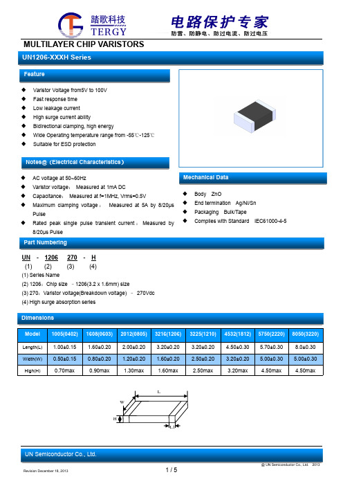
MULTILAYER CHIP VARISTORS
UN1206-XXXH Series
Feature
Varistor Voltage from5V to 100V Fast response time Low leakage current High surge current ability Bidirectional clamping, high energy Wide Operating temperature range from -55℃-125℃ Suitable for ESD protection
Dimensions
Model 1005(0402) 1608(0603) 2012(0805) 3216(1206) 3225(1210) 4532(1812) 5750(2220) 8050(3220)
Length(L) Width(W) High(H)
1.00±0.15 0.50±0.15 0.70max
Notes@(Electrical Characteristics)
AC voltage at 50~60Hz Varistor voltage: Measured at 1mA DC Capacitance: Measured at f=1MHz, Vrms=0.5V Maximum clamping voltage : Measured at 5A by 8/20µs
LC1206A电源芯片资料
LC1206A电源芯片资料__ LC 1205A电源集成芯片简述:__ 楦咝阅堋㈦流模式PWM高洪_P控制器集成路,榧译控制器源O。
芯片具有特的交流哼^零信zyc出控制路,可出同步的交流哼^零信用於^__ 楦咝阅堋㈦流模式PWM高洪_P控制器集成路,榧译制器源O。
芯片具有特的交流哼^零信zyc出控制路,可出同步的交流哼^零信用於^器、可控硅等M行^零切Q控制,亩提高系y的可靠性,降低切Qp耗,延L^器勖。
高集成的OtO大地化了路Y,降低了系y成本。
戎800V高耐汗β书_P,在90-300V的W汗忍峁└哌_6W 的Bm出功率。
高性r比的pO型u作工生a的控制芯片,Y合高汗β使艿囊惑w化封b最大程度上s了a品的整w成本。
源控制器可工作於典型的反激路拓渲校成的AC/DC源DQ器。
通^AC 翰ㄐ蔚姆治觯炔侩路右集O_路的三O管在AC 旱拿^零c出一定的上升波形,亩在外部通^一光耦蚀_出^零信oMCU 系y。
工作於初耗Jr特的直接反控制大幅提高了系y突ld的速度和能力,避免了鹘y的PSRY的d禾F象;工作於次反模式rt可精_的控制出壕度。
S械尿与路使_P管始K工作於R界和B,提高了系y的工作效率,使系y可以pM足“能源之星”等P於待C功耗和效率的JC要求。
IC 炔窟提供了完善的^dc短路保o功能,可出^d、出短路等常rM行快速保o,提高了源的可靠性。
IC炔窟集成了^囟缺Wo功能,在芯片^岬那r下降低工作l率或P]出。
F可提供M足ROHS始熬G色h保要求DIP7 史庋ba品。
主要特c?戎媒涣鬟^零检测及零点信出?支持初夯虼渭?戎800V 高汗β书_P?戎酶嚎焖与流源?系y待C功耗可低至0.10W?戎眠^骸⑶号c短路保o功能?精_囟妊a,精_逐L期流控制?智能自mOTP ^囟缺Wo功能?DQ效率M足能源之星2022年-V5 要求?宽W狠出功率6W,峰值输出8W ?C少外元件,低整C成本,高可靠性用I域?家控制器源?器控制器源?小家源。
1206 50r贴片电阻
1206 50r贴片电阻什么是1206 50r贴片电阻?1206 50r贴片电阻是一种被广泛使用的电子元件,是电子设备中常见的电阻器。
其中,“1206”代表了该电阻的尺寸,50r代表了其电阻值。
在电子领域中,贴片电阻的尺寸通常由其长度和宽度来表示,以毫米为单位。
1206贴片电阻的尺寸为1.2毫米长和0.6毫米宽。
为什么要使用1206 50r贴片电阻?贴片电阻主要用于调整和限制电流的流动,以及改变电路中的电压。
它们在电子设备中的应用非常广泛,因为它们具有小尺寸、容易安装和耐用等优点。
1206 50r贴片电阻是尺寸较大的一种贴片电阻,因此在电路中较为容易识别和操作。
如何使用1206 50r贴片电阻?使用1206 50r贴片电阻的第一步是确认其正确的引脚连接。
通常,它们具有两个金属引脚,其中一个是电阻的输入端,另一个是输出端。
将电阻与正确的引脚连接,以确保其可以正确工作。
接下来,根据所需的电阻值,在电路中正确选择并连接1206 50r贴片电阻。
贴片电阻的电阻值标识通常以欧姆(ohms)为单位,并在电阻身上使用彩色或数字编码进行标记。
在这种情况下,50r代表电阻值为50欧姆。
将电阻与电路中的其他元件正确连接,以实现所需的电流或电压控制。
这通常涉及将电阻插入电路中的正确位置,并使用焊接或其他连接方法进行固定。
最后,确保电路连接安全可靠,并进行必要的测试和检查。
使用仪器检测电阻的电阻值,并确认其是否符合制造商提供的规格。
总结:1206 50r贴片电阻是一种常用的电子元件,用于调整和限制电流流动以及改变电路中的电压。
使用它们的第一步是确认正确的引脚连接,然后根据所需的电阻值选择和连接电阻。
最后,确保电路连接安全可靠,并进行必要的测试和检查。
通过正确使用和处理1206 50r贴片电阻,可以确保电子设备的正常运行。
Littelfuse力特1206自恢复保险丝规格书
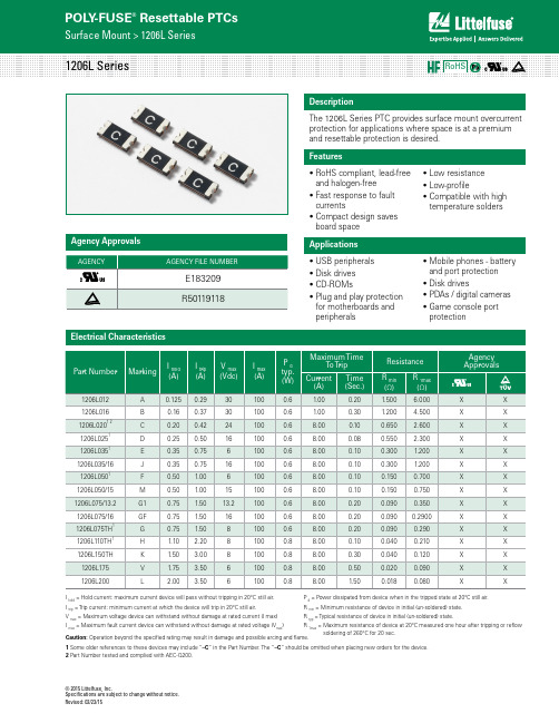
© 2015 Littelfuse, Inc.Specifications are subject to change without notice. Revised: 02/23/15The 1206L Series PTC provides surface mount overcurrent protection for applications where space is at a premium and resettable protection is desired.Electrical CharacteristicsI hold = Hold current: maximum current device will pass without tripping in 20°C still air. I trip = Trip current: minimum current at which the device will trip in 20°C still air.V max = Maximum voltage device can withstand without damage at rated current (I max) I max = Maximum fault current device can withstand without damage at rated voltage (V max )P d = Power dissipated from device when in the tripped state at 20°C still air.R min = Minimum resistance of device in initial (un-soldered) state.R typ = Typical resistance of device in initial (un-soldered) state.R 1max =M aximum resistance of device at 20°C measured one hour after tripping or reflow soldering of 260°C for 20 sec.DescriptionAgency ApprovalsFeaturesApplications• R oHS compliant, lead-free and halogen-free • F ast response to fault currents • C ompact design saves board space• L ow resistance • L ow-profile • C ompatible with high temperature solders• U SB peripherals • D isk drives • C D-ROMs • P lug and play protection for motherboards and peripherals• M obile phones - battery and port protection • D isk drives • P DAs / digital cameras • G ame console port protectionCaution: Operation beyond the specified rating may result in damage and possible arcing and flame.1 Some older references to these devices may include “–C “ in the Part Number. The “–C “ should be omitted when placing new orders for the device.2 Part Number tested and complied with AEC-Q200.© 2015 Littelfuse, Inc. Specifications are subject to change without notice.Revised: 02/23/15T emperature Rerating Curve-40-30-20-100102030405060708010%30%50%70%90%110%130%150%170%Temperature (°C)PercentageofRatedCurrentAverage Time Current CurvesThe average time current curves and Temperature Rerating curve performance is affectedby a number or variables, and these curves provided as guidance only. Customer mustverify the performance in their application..12A.16A.2A.25A.35A.35A/15V.5A.5A/15V.75A1.A1.1A1.5A2.A100001210L OLD.5A.1A.2A.35A.5A.75A1.1A1.5A1.75A2.A0.010.11101000.1110TimeinSecondsCurrent in Amperes1210L.5A.1A.2A.35A.5A.75A.75A/241.1A1.5A1.75A2.A0.010.11101000.1110TimeinSecondsCurrent in Amperes1206L.12A.16A.2A.25A.35A,.35A/15V.5A,.5A/15V.75A.75A/13.2V1.1A1.5A1.75A2.ANotes: The temperature rerating data is only for reference, please contact Littelfuse technical support for detail temperature rerating information.© 2015 Littelfuse, Inc.Specifications are subject to change without notice. Revised: 02/23/15Environmental SpecificationsPhysical Specifications-- All temperature refer to topside of the package, measured on the package body surface -- If reflow temperature exceeds the recommended profile, devices may not meet the performance requirements-- Recommended reflow methods: IR, vapor phase oven, hot air oven, N 2 environment for lead-- Recommended maximum paste thickness is 0.25mm (0.010 i nch)-- Devices can be cleaned using standard industry methods and solvents -- Devices can be reworked using the standard industry practices© 2015 Littelfuse, Inc.Specifications are subject to change without notice.Revised: 02/23/15(.040)MARKING CODE VARIES WITH AMPERAGE RATING(SEE ELECTRICAL CHARACTERISTICS CHART)SHOWN IS 1.0 AMP RATINGWARNING• Users shall independently assess the suitability of these devices for each of their applications• Operation of these devices beyond the stated maximum ratings could result in damage to the devices and lead to electrical arcing and/or fire• These devices are intended to protect against the effects of temporary over-current or over-temperature conditions and are not intended to perform as protective devices where such conditions are expected to be repetitive or prolonged in duration• Exposure to silicon-based oils, solvents, electrolytes, acids, and similar materials can adversely affect the performance of these PPTC devices• These devices undergo thermal expansion under fault conditions, and thus shall be provided with adequate space and be protected against mechanical stresses • Circuits with inductance may generate a voltage (L di/dt) above the rated voltage of the PPTC device.© 2015 Littelfuse, Inc.Specifications are subject to change without notice. Revised: 02/23/15=10,000 Y =4,000 W =3,000 P =2,000Tape & Reel-A: Automotive grade Blank: Standard version© 2015 Littelfuse, Inc.Specifications are subject to change without notice.Revised: 02/23/15。
Ralec合金电阻规格书
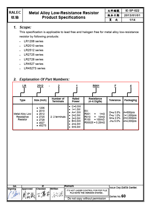
(0.645±0.254) (0.787±0.254)
LR2512
LR2725 LR2728
0.5 ~ 3.0
1.0 & 1.5
3.1 ~ 4.0 4.1 ~75.0
75.1 ~ 100.0
0.5 ~ 3.0
2.0
3.1 ~ 4.0
0.246±0.010 (6.248±0.254)
4.1 ~75.0
文件編號 版本日期 頁次
IE-SP-022 2013/01/01
3/14
3.1 Power Derating Curve: Operating Temperature Range: - 55 ~+170 ℃ For resistors operated in ambient temperatures 70°C, power rating shell be derated in accordance with the curve below:
Do not copy without permission
Issue Dep.DATA Center.
Series No.60
RALEC
旺詮
Metal Alloy Low-Resistance Resistor Product Specifications
文件編號 版本日期 頁次
IE-SP-022 2013/01/01
5/14
Type LR4527S (without heat sink)
LR4527
Maximum
Power Resistance
Rating Range (mΩ)
L
(Watts)
Dimensions - in inches (millimeters)
大毅1206毫欧低阻采样电阻RL12(20-91)系列选型手册
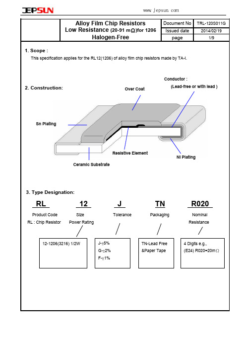
深圳捷比信--高品质精密元件供应商
www.jepsun.com
9. Label 9.1 Manufacture Label : Date Code QTY: 5000 PCS Lot No: T336B0026K C6 1336
page
Resistance Tolerance Type
R020
RL12JT
J
Manufacture Label
9.2 Customer Label( By customer request ): Lead-Free Products
TA-I TECH
Product Spec. Customer No:
1206 5%(T) 0.02Ω 105A702723 RL12JTNR020
LEAD FREE
04.05.21
Date
Year Month 10. Recommended land patterns
Land pattern Type Size
Solderability
IEC60115-1-4.17 JIS-C5201-1-4.17
245±5℃ solder, 2±0.5 sec dwell. Solder : Sn96.5 / Ag3.0 / Cu0.5
Robustness of Termination (Bending Strength)
Sn Plating
Resistive Element Ceramic Substrate
Littelfuse 1206大小快速作用熔断器说明书
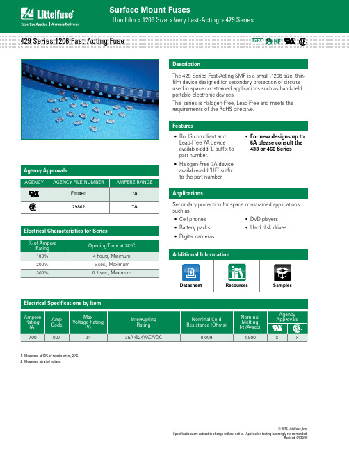
© 2015 Littelfuse, Inc. Specifications are subject to change without notice.Revised: 04/30/15DescriptionThe 429 Series Fast-Acting SMF is a small (1206 size) thin-film device designed for secondary protection of circuits used in space constrained applications such as hand-held portable electronic devices.This series is Halogen-Free, Lead-Free and meets the requirements of the RoHS directive.Agency ApprovalsElectrical Characteristics for Series Features• RoHS compliant andLead-Free 7A deviceavailable-add ‘L’ suffix topart number.• Halogen-Free 7A deviceavailable-add ‘HF’ suffixto the part number• For new designs up to5A please consult the433 or 466 Series ApplicationsElectrical Specifications by Item1. Measured at 10% of rated current, 25ºC.2. Measured at rated voltage.• Cell phones• Battery packs• Digital cameras• DVD players• Hard disk drives. Secondary protection for space constrained applications such as:Specifications are subject to change without notice. Application testing is strongly recommended.© 2015 Littelfuse, Inc.Specifications are subject to change without notice. Revised: 04/30/157ATIMEINSECONDSCURRENT IN AMPERES0.010.10.11110100101000.001 Soldering ParametersNote:1. Rerating depicted in this curve is in addition to the standard derating of 25% forcontinuous operation.Example:For continuous operation at 70 degrees celsius, the fuse should be deratedas follows:I = (0.75)(0.80)IRAT= (0.60)IRAT2. The temperature derating curve represents the nominal conditions. For questionsabout temperature derating curve, please consult Littelfuse technical supportfor assistance.© 2015 Littelfuse, Inc.Specifications are subject to change without notice.Revised: 04/30/15DimensionsREFLOW SOLDERRECOMMENDED PAD LAYOUTS1.52(.080")1.14Part Numbering SystemPackagingPart Marking System0429 007. WRM L HFSERIES AMP CodeQUANTITY CodeL = Lead-Free device and RoHS compliant device Refer to Amp Code Column of Electrical characteristics table WRM = 3000 pieces, Tape and Reel‘HF’ SUFFIXHALOGEN FREE ITEM。
1206全彩贴片LED-1206全彩共阴LED规格书

SPECIFICATION FOR APPROVAL
客户 Customer:
客户品号 Customer P/N:
鑫光硕品号 Xgs Model:
规格 Specification :
XGS-PB3216UEUGUB-04-B SMD 1206 RGB共阴 20MA
制作 Prepared By:
审核 Checked By:
IF
25
Reverse Voltage
VR
5
Operating Temperature Range
Topr
-40℃~85℃
Storage Temperature Range
Tstg
-40℃~100℃
IFP condition: pulse width ≤1ms ,duty cycle ≤1/10
20
0/1
60cm/min,2 times
(2)Criteria of judging the damage
Item
Forward voltage Reverse current
Luminous intensity
Wave length
Appearance
Symbol VF IR IV
λD/λP /
◆ Applications:
Automotive and Telecommunication Flat backlight for LCD ,switch and symbol in telephone and fax General use for indicators
◆ Package Dimensions:
◆ Electrical Optical Characteristics(Ta=25℃)
1206封装系列贴片保险丝

0.20
0.6
8.00
0.20
0.6
8.00
0.20
0.6
8.00
0.30
0.6
8.00
0.30
0.6
8.00
0.30
0.6
8.00
0.30
0.6
8.00
0.30
0.6
8.00
0.30
0.8
8.00
0.30
0.8
8.00
0.30
0.8
8.00
0.50
0.8
8.00
1.50
Resistance
R i min ()
24.0
100
JSMD1206-035
J3
16.0
100
JSMD1206-035/30 J3
30.0
100
JSMD1206-050
J5
6.0
100
JSMD1206-050/8 J5
8.0
100
JSMD1206-050/16 J5
16.0
100
JSMD1206-050/24 J5
24.0
100
JSMD1206-075
0.75
0.75 1.00 1.00 1.00 1.10 1.10 1.10 1.50 1.50 1.75 2.00
I trip @25°C
(A) 0.15 0.15 0.25 0.25 0.29 0.29 0.46 0.46 0.50 0.50 0.75 0.75 1.00 1.00 1.00 1.00 1.50
Pb-Free Assembly 3℃/second mac.
150℃ 200℃ 60~180 seconds
ILAS1206ER102V;ILAS1206ER121V;ILAS1206ER301V;ILAS1206ER600V;ILAS1206ER601V;中文规格书,Datasheet资料

Document Number: 34103For technical questions, contact: magnetics@Chip Array Ferrite BeadsILAS-1206Vishay DaleMECHANICAL SPECIFICATIONSSolderability: 90 % coverage after 5 s dip in 235 °C solder following 60 s preheat at 120 °C to 150 °C and type R flux dip Resistance to Solder Heat: 10 s in 260 °C solder, after preheat and flux per aboveTerminal Strength: 1.2 kg (2.64 lbs) minimum for 30 s Beam Strength: 2.0 kg (4.4 lbs) minimumFlex: 0.079" [2 mm] min. mounted on 0.063" [1.6 mm] thick PC boardFEATURES•Combines four single 0603 chips into one package to reduce board space and placement time•Highly effective in high density applications•0.031" [0.8 mm] terminal pitch makes it easy toapply EMI prevention in multiple-lines such as connectors amd IC pins•Material and construction design minimize crosstalk between adjacent circuits•Compliant to RoHS directive 2002/95/ECENVIRONMENTAL SPECIFICATIONSOperating Temperature: - 55 °C to + 125 °C Thermal Shock: 300 cycles, - 40 °C to + 125 °CBiased Humidity: 85 % RH at 85 °C, 1000 h at full rated currentSTANDARD ELECTRICAL SPECIFICATIONSZ± 25 % AT 100 MHz(Ω)DCR MAX.(Ω)RATED DC CURRENT(mA)SIGNAL SPEED600.12300Standard 1200.21503000.41006000.610010000.850DESCRIPTIONILAS-1206120± 25 %ERe 3MODELIMPEDANCE VALUEIMPEDANCE TOLERANCEPACKAGE CODEJEDEC LEAD (Pb)-FREE STANDARDGLOBAL PART NUMBERILAS1206ER121V PRODUCT FAMILYSIZEPACKAGE CODEIMPEDANCE VALUEIMPEDANCE TOLERANCEILAS-1206Vishay Dale Chip Array Ferrite Beads For technical questions, contact: magnetics@ Document Number: 34103Legal Disclaimer Notice VishayDisclaimerALL PRODU CT, PRODU CT SPECIFICATIONS AND DATA ARE SU BJECT TO CHANGE WITHOU T NOTICE TO IMPROVE RELIABILITY, FUNCTION OR DESIGN OR OTHERWISE.Vishay Intertechnology, Inc., its affiliates, agents, and employees, and all persons acting on its or their behalf (collectively,“Vishay”), disclaim any and all liability for any errors, inaccuracies or incompleteness contained in any datasheet or in any other disclosure relating to any product.Vishay makes no warranty, representation or guarantee regarding the suitability of the products for any particular purpose or the continuing production of any product. To the maximum extent permitted by applicable law, Vishay disclaims (i) any and all liability arising out of the application or use of any product, (ii) any and all liability, including without limitation special, consequential or incidental damages, and (iii) any and all implied warranties, including warranties of fitness for particular purpose, non-infringement and merchantability.Statements regarding the suitability of products for certain types of applications are based on Vishay’s knowledge of typical requirements that are often placed on Vishay products in generic applications. Such statements are not binding statements about the suitability of products for a particular application. It is the customer’s responsibility to validate that a particular product with the properties described in the product specification is suitable for use in a particular application. Parameters provided in datasheets and/or specifications may vary in different applications and performance may vary over time. All operating parameters, including typical parameters, must be validated for each customer application by the customer’s technical experts. Product specifications do not expand or otherwise modify Vishay’s terms and conditions of purchase, including but not limited to the warranty expressed therein.Except as expressly indicated in writing, Vishay products are not designed for use in medical, life-saving, or life-sustaining applications or for any other application in which the failure of the Vishay product could result in personal injury or death. Customers using or selling Vishay products not expressly indicated for use in such applications do so at their own risk and agree to fully indemnify and hold Vishay and its distributors harmless from and against any and all claims, liabilities, expenses and damages arising or resulting in connection with such use or sale, including attorneys fees, even if such claim alleges that Vishay or its distributor was negligent regarding the design or manufacture of the part. Please contact authorized Vishay personnel to obtain written terms and conditions regarding products designed for such applications.No license, express or implied, by estoppel or otherwise, to any intellectual property rights is granted by this document or by any conduct of Vishay. Product names and markings noted herein may be trademarks of their respective owners.Material Category PolicyVishay Intertechnology, Inc. hereb y certifies that all its products that are identified as RoHS-Compliant fulfill the definitions and restrictions defined under Directive 2011/65/EU of The European Parliament and of the Council of June 8, 2011 on the restriction of the use of certain hazardous substances in electrical and electronic equipment (EEE) - recast, unless otherwise specified as non-compliant.Please note that some Vishay documentation may still make reference to RoHS Directive 2002/95/EC. We confirm that all the products identified as being compliant to Directive 2002/95/EC conform to Directive 2011/65/EU.Revision: 12-Mar-121Document Number: 91000分销商库存信息:VISHAYILAS1206ER102V ILAS1206ER121V ILAS1206ER301V ILAS1206ER600V ILAS1206ER601V。
1206 电阻通用规格书
o d u c t s p e c i f i c a t i o n – F e b r u a r y 6, 2013 V .5S u p e r s e d e s D a t e o f M a r . 06, 2003Y A G E O B R A N D o r d e r i n g c o d eGLOBAL PART NUMBER (PREFERRED )RC1206 X R - XX XXXX L(1) (2) (3) (4) (5) (6)(1) TOLERANCED = ±0.5% F = ±1%J = ±5% (for Jumper ordering, use code of J)(2) PACKAGING TYPER = Paper taping reel(3) TEMPERATURE COEFFICIENT OF RESISTANCE– = Base on spec(4) TAPING REEL07 = 7 inch dia. Reel 10 = 10 inch dia. Reel 13 = 13 inch dia. Reel(5) RESISTANCE VALUEThere are 2~4 digits indicated the resistor value. Letter R/K/M is decimal point, no need to mention the last zero after R/K/M, e.g.1K2, not 1K20.Detailed resistance rules show in table of “Resistance rule of global part number”.(6) DEFAULT CODELetter L is system default code for order only (Note)ORDERING INFORMATION - GLOBAL PART NUMBER & 12NC Both part numbers are identified by the series, size, tolerance, packing type, temperature coefficient, taping reel and resistance value.SCOPEThis specification describes RC1206 series chip resistors with lead-free terminations made by thick film process.APPLICATIONS● All general purpose applicationFEATURES● Halogen Free Epoxy●RoHS compliant- Products with lead freeterminations meet RoHS requirements- Pb-glass contained in electrodes,resistor element and glass are exempted by RoHS●Reducing environmentally hazardous wastes●High component and equipment reliability● Saving of PCB space●None forbidden-materials used in products/productionO RDERING EXAMPLEThe ordering code of a RC1206 chip resistor, value 56 X with ±1% tolerance, supplied in 7-inch tape reel is: RC1206FR-0756RL.NOTE1. All our RSMD products meet RoHS compliant and Halogen Free. "LFP" of the internal 2D reel label mentions "Lead Free Process"2. On customized label, "LFP" or specific symbol can be printedResistance rule of global part numberResistance code rule Example0R0R = Jumper XRXX(1 to 9.76 Ω) 1R = 1 Ω1R5 = 1.5 Ω9R76 = 9.76 ΩXXRX(10 to 97.6 Ω) 10R = 10 Ω97R6 = 97.6 ΩXXXR(100 to 976 Ω) 100R = 100 ΩXKXX(1 to 9.76 K Ω) 1K = 1,000 Ω9K76 = 9760 ΩXMXX(1 to 9.76 M Ω) 1M = 1,000,000 Ω9M76= 9,760,000 Ω12NC CODE2322 / 2350 XXX XXXXX L(1) (2) (3) (4)TYPE/ 1206 START IN (1) TOL. (%) RESISTANCERANGE PAPER / PE TAPE ON REEL (units) (2) 5,000 10,000/not preferred 20,000RC01 2322 ±5% 1 to 10 M Ω711 61xxx711 51xxx711 81xxx RC02 2322 ±1% 1 to 10 M Ω 724 6xxxx 724 7xxxx 724 8xxxxHRC01 2350±5% 11 to 22 M Ω 520 10xxx-- Jumper 2322 - 0 Ω 711 91032 711 91005711 92004P H Y C O M P B R A N D o r d e r i n g c o d e sBoth GLOBAL PART NUMBER (preferred) and 12NC (traditional) codes are acceptable to order Phycomp brand products. GLOBAL PART NUMBER (PREFERRED ) For detailed information of GLOBAL PART NUMBER and ordering example, please refer to page 2.Resistance decade (3) Last digit 0.01 to 0.0976 X 00.1 to 0.976 X 71 to 9.76 X 810 to 97.6 X 9100 to 976 X 11 to 9.76 K X 210 to 97.6 K X 3100 to 976 K X 41 to 9.76 M X 510 to 97.6 M X6Example: 0.02X = 0200 or 200 0.3 X = 3007 or 3071 X=1008 or 10833 K X = 3303 or 333 10 M X = 1006 or 106Last digit of 12NC(1) The resistors have a 12-digit ordering code starting with 2322 / 2350.(2) The subsequent 4 or 5 digits indicate the resistor tolerance andpackaging. (3) The remaining 4 or 3 digits represent the resistance value with thelast digit indicating the multiplier as shown in the table of “Last digit of 12NC”. (4) Letter L is system default code for order only (Note) O RDERING EXAMPLEThe ordering code of a RC02 resistor, value 56 X with ±1% tolerance, supplied in tape of 10,000 units per reel is: 232272465609L or RC1206FR-0756RL.NOTE1. All our RSMD products meet RoHS compliant and Halogen Free. "LFP" of the internal 2D reel label mentions "Lead Free Process"2. On customized label, "LFP" or specific symbol can be printedCONSTRUCTIONThe resistor is constructed on top of a high-grade ceramic body.Internal metal electrodes are added on each end to make the contacts to the thick film resistive element. The composition of the resistive element is a noble metal imbedded into a glass and covered by a second glass to prevent environment influences. The resistor is laser trimmed to the rated resistance value. The resistor is covered with a protective epoxy coat, finally the two external terminations (matte tin on Ni-barrier) are added. See fig.3DIMENSIONSTYPE RC1206L (mm)3.10 ± 0.10W (mm) 1.60 ± 0.10H (mm) 0.55 ± 0.10I 1 (mm) 0.45 ± 0.20I 2 (mm)0.40 ± 0.20T able 1O U T L I N E SMARKINGRC1206No markingFor further marking information, please refer to data sheet “Chip resistors marking”ELECTRICAL CHARACTERISTICS CHARACTERISTICS RC1206 1/4 WOperating Temperature Range –55 °C to +155 °CMaximum Working Voltage 200 V Maximum Overload Voltage 400 V Dielectric Withstanding Voltage500 VResistance Range5% (E24) 1 Ω to 22 M Ω1% (E24/E96) 1 Ω to 10 M Ω0.5% (E24/E96) 10 to 1 M ΩΩZero Ohm Jumper < 0.05 ΩTemperature Coefficient1 Ω ≤ R ≤ 10 Ω±200 ppm/°C ±200 ppm/°C 10 M Ω < R ≤ 22 M Ω10 Ω < R ≤ 10 M Ω±100 ppm/°CJumper CriteriaRated Current 2 A Maximum Current10 AFOOTPRINT AND SOLDERING PROFILESFor recommended footprint andsoldering profiles, please refer to data sheet “Chip resistors mounting”.T able 2PACKING STYLE AND PACKAGING QUANTITY PRODUCT TYPE PACKING STYLEREEL DIMENSIONQUANTITY PER REELRC1206 Paper Taping Reel (R) 7" (178 mm) 5,000 units10" (254 mm) 10,000 units13" (330 mm)20,000 unitsNOTE1. For paper tape and reel specification/dimensions, please see the special data sheet “Chip resistors packing”T able 3Packing style and packaging quantityFUNCTIONAL DESCRIPTIONP O W E R R A T I N GRC1206 rated power at 70°C is 1/4 W R ATED VOLTAGEThe DC or AC (rms) continuous working voltage corresponding to the rated power is determined by the following formula:V=R)(P Xor max. working voltage whichever is less WhereV=Continuous rated DC or AC (rms) working voltage (V) P=Rated power (W) R=Resistance value (X )TESTS AND REQUIREMENTSTEST TESTMETHOD PROCEDURE REQUIREMENTSTemperature Coefficient of Resistance (T.C.R.) IEC 60115-1 4.8 At +25/–55 °C and +25/+125 °C Refer to table 2Formula:T.C.R= ------------------------- ×106 (ppm/°C)Wheret1=+25 °C or specified room temperaturet2=–55 °C or +125 °C test temperatureR1=resistance at reference temperature in ohmsR2=resistance at test temperature in ohmsLife/Endurance IEC 60115-1 4.25.1 At 70±5 °C for 1,000 hours, RCWV applied for1.5 hours on, 0.5 hour off, still air required ±(1.0%+0.05 ) for 1%,Ω0.5% tol.±(3.0%+0.05 Ω) for 5% tol. <100 mΩ for JumperHigh Temperature Exposure/ Endurance at Upper Category Temperature IEC 60068-2-2 1,000 hours at 155±5 °C, unpowered ±(1.0%+0.05 ) for 1%,Ω0.5% tol.±(2.0%+0.05 Ω) for 5% tol.<50 mΩ for JumperMoisture Resistance MIL-STD-202G Method-106G Each temperature / humidity cycle is defined at 8hours, 3 cycles / 24 hours for 10d. with 25 °C /65 °C 95% R.H, without steps 7a & 7b,unpoweredParts mounted on test-boards, withoutcondensation on partsMeasurement at 24±2 hours after test conclusion±(0.5%+0.05 ) for 1%,Ω0.5% tol.±(2.0%+0.05 Ω) for 5% tol.<100 mΩ for JumperThermal Shock MIL-STD-202G Method-107G -55/+125 °CNumber of cycles required is 300. DevicesunmountedMaximum transfer time is 20 seconds. Dwell timeis 15 minutes. Air – Air ±(0.5%+0.05 ) for 1%,Ω0.5% tol.±(1%+0.05 Ω) for 5% tol.<50 mΩ for JumperShort Time Overload IEC60115-1 4.13 2.5 times of rated voltage or maximum overloadvoltage whichever is less for 5 sec at roomtemperature±(1.0%+0.05 ) for 1%,Ω0.5% tol.±(2.0%+0.05 Ω) for 5% tol.<50 mΩ for JumperNo visible damageT able 4 Test condition, procedure and requirementsR2–R1R1(t2–t1)TEST TESTMETHOD PROCEDURE REQUIREMENTSBoard Flex/ Bending IEC 60068-2-21 Chips mounted on a 90mm glass epoxy resinPCB (FR4)2 mm bendingBending time: 60±5 seconds±(1.0%+0.05 Ω)<50 mΩ for JumperNo visible damageLow Temperature Operation IEC 60068-2-1 The resistor shall be subjected to a DC ratedvoltage for 1.5 h-on, 0.5 h-off, at -55±3 °CThis constitutes shall be repeated for 96 hoursHowever the applied voltage shall not exceedthe maximum operating voltage±(0.5%+0.05 )Ωfor 1%,0.5% tol.±(1.0%+0.05 Ω) for 5% tol.No visible damageInsulation Resistance IEC 60115-1 4.6 Rated continuous overload voltage (RCOV)for 1 minuteType RC1206Voltage (DC) 100 V≥10 GΩDielectric Withstand Voltage IEC 60115-1 4.7 Maximum voltage (V rms) applied for 1 minuteType RC1206Voltage (AC) 500 V rmsNo breakdown or flashoverResistance to Solvent IPC/JEDEC J-STD-020D lsopropylalcohol (C3H7OH) followed bybrushingNo smearedNoise IEC 60115-1 4.12 Maximum voltage (Vrms) applied Resistors range ValueR < 100 Ω10 dB100 Ω≤ R < 1 KΩ20 dB1 KΩ≤ R < 10 KΩ30 dB10 KΩ≤ R < 100 KΩ40 dB100 KΩ≤ R < 1 MΩ46 dB1 MΩ≤ R ≤ 22 MΩ48 dBHumidity IEC 60115-1 4.37 Steady state for 1000 hours at 40 °C / 95% R.H.RCWV applied for 1.5 hours on and0.5 hour off ±(1.0%+0.05 ) for 1%,Ω0.5% tol.±(2.0%+0.05 Ω) for 5% tol. <100 mΩ for JumperTEST TESTMETHODPROCEDURE REQUIREMENTSIntermittent Overload IEC 60115-1 4.39 2.5 times of rated voltage or maximumoverload voltage whichever is less for 1 secondon and 25 seconds off; total 10,000 cycles±(1.0%+0.05 ) for 1%,Ω0.5% tol.±(2.0%+0.05 Ω) for 5% tol.<100 mΩ for JumperSolderability- Wetting IPC/JEDEC J-STD-002B test B Electrical Test not requiredMagnification 50XSMD conditions:1st step: method B, aging 4 hours at 155 °Cdry heat2nd step: leadfree solder bath at 245±3 °CDipping time: 3±0.5 seconds Well tinned (≥95% covered) No visible damage- Leaching IPC/JEDEC J-STD-002B test D Leadfree solder, 260 °C, 30 secondsimmersion timeNo visible damage- Resistance to Soldering Heat IEC 60068-2-58 Condition B, no pre-heat of samplesLeadfree solder, 260 °C, 10 secondsimmersion timeProcedure 2 for SMD: devices fluxed andcleaned with isopropanol±(0.5%+0.05 ) for 1%,Ω0.5% tol.±(1.0%+0.05 Ω) for 5% tol.<50 mΩ for JumperNo visible damageREVISION HISTORYREVISION DATE CHANGE NOTIFICATION DESCRIPTIONVersion 5 Feb 06, 2013 - -Marking updated-Add 0.5% toleranceVersion 4 Jul 02, 2009 - - Test Items and methods updated- Test requirements upgradedVersion 3 Jul 15, 2008 - - Change to dual brand datasheet that describe RC1206 with RoHS compliant- Description of "Halogen Free Epoxy" added- Define global part numberVersion 2 Sep 03, 2004 - - New datasheet for 1206 thick film 1% and 5% with lead-free terminations- Replace the 1206 part of pdf files: RC01_11_21_31_5, RC02_12_22_32_10,and HRC01_5_4- Test method and procedure updated- PE tape added (paper tape will be replaced by PE tape)- High ohmic products combined into standard products.“ Yageo reserves all the rights for revising the content of this datasheet without further notification, as long as the products itself are unchanged. Any product change will be announced by PCN.”國巨股份有限公司 新北市新店區寶橋路233之1號3樓 3F., 233-1, Baoqiao Rd., Xindian, Taipei 231, Taiwan t. +886.2.2917.7555 f. +886.2.2917.5078To remove AC0603/0805/1206 and RC0603/0805/1206 markingJanuary 16th , 2013Dear Customers,Yageo would like to announce that we will remove the Resistance Marking on Yageo’s R Chip case sizes 0603/0805/1206 products from March 1st 2013 for the purposes of reducing unnecessary chemical usages for environmental protections. To identify the product resistance value, the label on the reels has been serving and will continue serving the purposes. As for the product performance, features, specifications, manufacturing process and locations remain the same. That is to say the elimination of the resiatance marking on the product appearance has no impact on the product functionality and you can feel free to use it for your current applications.Yageo has provided no resistance marking on R Chip 0402/0201/01005 and on the entire MLCC family ever since. Given Yageo has been devoted to being eco-friendly, we decide to eliminate the marking on the R Chip of the sizes of 0603 and the above as soon as possible. There will be a short period of time that both types of the products, with marking and without marking, co exist while we are changing the production lines one by one. We highly appreciate your understanding that we may ship the products in parallel for some time. Yageo commits that we will make full efforts to shorten the overlapping period as much as we can.We truly appreciate being your business partner and serving your passivecomponent needs. If there are any questions, please feel free to contact Yageo’s sales offices.Sincerely Yours,Product Business Unit, R chip product marketing Yageo CorporationNotice Notice通知信取消AC及RC 0603/0805/1206系列字码印制2013年1月15日亲爱的客户,您好为了维护环境并减少非必要的化学原料使用,国巨在此通知您:自2013年3月1日起,将生产0603/0805/1206无字码印制的电阻。
RC1206中文资料
Thick Film Chip Resistor – General PurposeFeatures• Small and light weight• Excellent heat resistance and moisture resistance• Suitable size and packaging for surface mount assembly • RoHS CompliantApplications• For general purpose applications• For laptop and notebook computer, memory module, digital camera and telecommunication equipmentAbsolute Maximum Ratings & CharacteristicsProductNumbermm TolerancePower Rating @70˚CMAX Working Voltage MAXOverload VoltageTCR ppm/℃Resistance RangeRated WorkingTemperature±200 1Ω ~ 9.76Ω±100 10Ω ~ 1M ΩRC1206 3216J: ±5%F: ±1%1/4W 200V 400V ±2001.02M Ω ~ 10M Ω-55℃~+155℃*JumperProduct NumberJumper Rated CurrentResistanceRated Working Temperature RC1206 2A 50m Ω (max.)-55℃~+155℃RC1206 Power Derating CurveFor resistors operate in the ambient temperature over 70˚C, loading power ratio will de-rate in accordance with following curve.Soldering ConditionIR Reflow soldering Wave soldering (flow soldering)RC1206 Dimensions (in mm)ProductNumbermm L W H A BAverageWeight RC12063216 3.10 ± 0.101.55± 0.100.55 ± 0.100.50 ± 0.250.50 ± 0.20 8.84 mg Marking(1) ±5% Tolerance (J): 3 digits, the first two digits are significant figures; the third digit is numberof zeros to follow. Letter “R” is as decimal point; Letter “0” for jumper.(2) ±1% Tolerance (F): 4 digits, the first three digits are significant figures; the fourth digit isnumber of zeros. Letter “R” is as decimal point; Letter “0” for jumper.Examples:3 digits marking (±5%)4 digits marking (±1%)683 = 68x103Ω Jumper 6812 = 681x102Ω= 68000 Ω = 68KΩ = 68100 Ω = 68.1KΩ7R5 = 7.5 ΩRC1206 Test and RequirementsRequirement Test Item Test Method Test Condition±1% ±5% JumperTemperature Coefficient of Resistance(T.C.R.) JIS C 5201 4.8IEC 60115-1 4.8-55°C~+155,20°C isthe referencetemperatureWithin the specificationShort Time Overload JIS C 5201 4.13IEC 60115-1 4.132.5 times RCWV or max.overload voltage for 5seconds±(1.0%+0.05Ω) ±(2.0%+0.05Ω) <50mΩInsulation Resistance JIS C 5201 4.6IEC 60115-1 4.6Max. overload voltagefor 1 minute≥10GVoltage Proof JIS C 5201 4.7IEC 60115-1 4.71.42 times RCWV(RMS) for 1 minuteno breakdown or flashoverSubstrate Bending Test JIS C 5201 4.33IEC 60115-1 4.33Bending once with 5seconds for 3 mm±(1.0%+0.05Ω) ±(1.0%+0.05Ω) <50mΩResistance to soldering heat JIS C 5201 4.18IEC 60115 4.18260±5°C for 10 seconds±(0.5%+0.05Ω) ±(1.0%+0.05Ω) <50mΩLeaching JIS C 5201 4.18IEC 60115 4.18260±5°C for 60 seconds no leachingSolderability JIS C 5201 4.17IEC 60115-1 4.17245±5°C for 3 seconds. >95% coverageEndurance at upper category temperature JIS C 5201 4.23IEC 60115-1 2.23.2at +155°C for 1000 hrs ±(1.0%+0.05Ω) ±(1.5%+0.10Ω) <50mΩRapid change of temperature JIS C 5201 4.19IEC 60115-1 4.19-55°C to +155°C, 5cycles±(0.5%+0.05Ω) ±(1.0%+0.05Ω) <50mΩDamp heat with load JIS 5201 4.2440±2°C, 90~95% R.H.or max. working voltagefor 1000 hrswith 1.5hrs “ON” and 0.5hrs “OFF”±(2.0%+0.10Ω) ±(3.0%+0.10Ω) <100mΩEndurance JIS C 5201 4.25IEC 60115-1 4.25.170±2°C, RCWV or Max.working voltage for 1000hrs with 1.5 hrs“ON” and 0.5 hrs “OFF”±(2.0%+0.10Ω) ±(3.0%+0.10Ω) <100mΩNote: RCWV:Rated Continuous Working Voltage.RCWV= √Rated power (W) × Resistance value (R)RC1206Packing Information:Carrier Tape Dimensions (in mm)TypeABWEF P0 P1 P2ψD0T RC1206 1.90±0.1 3.50±0.2 8.0±0.2 1.75±0.13.5±0.054.0±0.14.0±0.052.0±0.05 1.5+0.1/-00.85±0.1Reel Dimensions (in mm)Reel DiameterPCS per ReelABCWT7’’ 5,000 180+0/-360+1/-0 13.0±0.29.0±0.5 11.4±1 13’’ 20,000 330±1 100±1 13.0±0.29.5±0.5 13.5±1Carton InformationPCS per CartonCarton Size300,000 400X400X200 ( in mm)RC1206 How to OrderRC1206 How to contact us:。
S-1206中文资料
*1
VIN
VOUT
Overcurrent protection circuit Reference voltage circuit − +
VSS
*1. Parasitic diode Figure 1
2
Seiko Instruments Inc.
元器件交易网
ULTRA LOW CURRENT CONSUMPTION AND LOW DROPOUT CMOS VOLTAGE REGULATOR Rev.1.1_00 S-1206 Series Product Name Structure
1. Product Name
S-1206 B xx xxxx G Package name (abbreviation) and packing specifications M3T1 : SOT-23-3, Tape U3T1 : SOT-89-3, Tape I6T2 : SNT-6A(H), Tape
*1
Output voltage value 12 to 52 (e.g. When output voltage is 1.2 V, it is expressed as 12.)
*1. Refer to the taping specifications.
- 1、下载文档前请自行甄别文档内容的完整性,平台不提供额外的编辑、内容补充、找答案等附加服务。
- 2、"仅部分预览"的文档,不可在线预览部分如存在完整性等问题,可反馈申请退款(可完整预览的文档不适用该条件!)。
- 3、如文档侵犯您的权益,请联系客服反馈,我们会尽快为您处理(人工客服工作时间:9:00-18:30)。
Thick Film Chip Resistor – Low OhmicFeatures• Low Inductance• Battery Charge Current Sensing• Highly Reliable Multilayer Electrode Construction• Higher Component and Equipment Reliability• Excellent Performance at High Frequency• Reduced Size of Final Equipment• RoHS CompliantApplications• For televisions, audio recorders, notebook computers,battery chargers, desktop computers and telecommunication equipment.Absolute Maximum Ratings & CharacteristicsType Name SizeCodeTolerancePowerRating@70°CMAXWorkingVoltageMAXOverloadVoltageTCR ppm/°C Resistance RangeRated WorkingTemperature±1500 0.010Ω ~ 0.018Ω (E-24)±1500 0.020Ω ~ 0.100Ω (E-24)RL1206 3216 J: ±5%Note1/4W 200V 400V±500 0.102Ω ~ 0.976Ω (E-96)-55°C~+155°CNote:±1% is available upon request.RL1206J SeriesPower Derating CurveFor resistors operate in the ambient temperature over 70°C, loading power ratio will derate in accordance with following curve.Soldering ConditionIR Reflow solderingWave soldering (Flow soldering)RL1206J SeriesDimensions (in mm)Type Name SizeCodeL WH A BAverageWeightRL1206 3216 3.10 ± 0.10 1.55± 0.100.55 ± 0.100.50 ± 0.250.50 ± 0.20 8.84 mg Marking InformationExamples:4 digits marking (±5%)R510 = 0.51 OhmRL1206J Series Test and RequirementsRequirement Test Item Test Method Test Condition±5%Temperature Coefficient of Resistance(T.C.R.) JIS C 5201 4.8IEC 60115-1 4.8-55°C~+155°C, 20°C isthe reference temperatureWithin the specificationShort Time Overload JIS C 5201 4.13IEC 60115-1 4.132.5 times RCWV or max.overload voltage for 5 seconds±2.0%Insulation Resistance JIS C 5201 4.6IEC 60115-1 4.6Max. overload voltagefor 1 minute≥10GVoltage Proof JIS C 5201 4.7IEC 60115-1 4.71.42 times RCWV (RMS) for 1minuteno breakdown or flashoverSubstrate Bending Test JIS C 5201 4.33IEC 60115-1 4.33Bending once with 5seconds for 3 mm±1.0%Resistance to soldering heat JIS C 5201 4.18IEC 60115 4.18260±5°C for 10 seconds ±1.0%Leaching JIS C 5201 4.18IEC 60115 4.18260±5°C for 60 seconds no leachingSolderability JIS C 5201 4.17IEC 60115-1 4.17245±5°C for 3 seconds >95% coverageEndurance at upper category temperature JIS C 5201 4.23IEC 60115-1 2.23.2at +155°C for 1000 hrs ±1.5%Rapid change of temperature JIS C 5201 4.19IEC 60115-1 4.19-55°C~+155°C, 5 cycles ±1.0%Damp heat with load JIS 5201 4.24 40±2°C, 90~95% R.H. or max.working voltage for 1000 hrswith 1.5hrs “ON” and 0.5 hrs“OFF”±3.0%Endurance JIS C 5201 4.25IEC 60115-1 4.25.170±2°C, or max. workingvoltage for 1000 hrs with 1.5hrs “ON” and 0.5 hrs “OFF”±3.0%Note: RCWV:Rated Continuous Working Voltage.RCWV= √Rated power (W) × Resistance value (R)RL1206J SeriesPacking Information:Carrier Tape Dimensions (in mm)Type NameABWEF P0P1P2ØD0T RL1206 1.9±0.1 3.5±0.2 8.0±0.2 1.75±0.13.5±0.054.0±0.1 4.0±0.05 2.0±0.05 1.5+0.1/-00.85±0.1Reel Dimensions (in mm)Reel DiameterPCS per Paper TapeABCWT7” 5,000 180+0/-360+1/-0 13.0±0.2 9.0±0.3 11.4±1Carton InformationPCS per CartonCarton Size (LxWxH)300,000 400X400X200 (in mm)RL1206J Series How to OrderRL1206J SeriesE-24 Series of Resistance ValueE-96 Series of Resistance Valuexxx (code) Ω xxx (code) Ω xxx(code)Ωxxx (code)Ω xxx (code)Ωxxx(code)Ωxxx (code)Ω R010 0.010 R011 0.011 R012 0.012R0130.013R0150.015 R016 0.016R0180.018R020 0.020 R022 0.022 R024 0.024R0270.027R0300.030 R036 0.036R0390.039R043 0.043 R056 0.056 R062 0.062R0680.068R0750.075 R082 0.082R0910.091xxx (code) Ω xxx (code) Ω xxx(code)Ωxxx (code)Ω xxx (code)Ωxxx(code)Ωxxx(code)Ω R100 0.100 R102 0.102 R105 0.105R1070.107R1100.110 R113 0.113R1150.115R118 0.118 R121 0.121 R124 0.124R1270.127R1300.130 R133 0.133R1370.137R140 0.140 R143 0.143 R147 0.147R1500.150R1540.154 R158 0.158R1620.162R165 0.165 R169 0.169 R174 0.174R1780.178R1820.182 R187 0.187R1910.191R196 0.196 R200 0.200 R205 0.205R2100.210R2150.215 R221 0.221R2260.226R232 0.232 R237 0.237 R243 0.243R2490.249R2550.255 R261 0.261R2670.267R274 0.274 R280 0.280 R287 0.287R2940.294R3010.301 R309 0.309R3160.316R324 0.324 R332 0.332 R340 0.340R3480.348R3570.357 R365 0.365R3740.374R383 0.383 R392 0.392 R402 0.402R4120.412R4220.422 R432 0.432R4420.442R453 0.453 R464 0.464 R475 0.475R4870.487R4990.499 R511 0.511R5230.523R536 0.536 R549 0.549 R562 0.562R5760.576R5900.590 R604 0.604R6190.619R634 0.634 R649 0.649 R665 0.665R6810.681R6980.698 R715 0.715R7320.732R750 0.750 R768 0.768 R787 0.787R8060.806R8250.825 R845 0.845R8660.866R887 0.887 R909 0.909 R931 0.931R9530.953R9760.976RL1206J Series How to contact us:。
