UDQ2549EB中文资料
金士顿e MMC 5.1嵌入式多媒体卡(e

Embedded Multi-Media Card(e•MMC™ 5.1)EMMC16G-IB29-PE90EMMC32G-IB29-PE90EMMC64G-IB29-PE90v1.0Product Features•Packaged managed NAND flash memory with e•MMC™ 5.1 interface•Backward compatible with all prior e•MMC™ specification revisions•153-ball JEDEC FBGA RoHS Compliant package•Operating voltage range:o VCCQ = 1.8 V/3.3 Vo VCC = 3.3 V•Operating Temperature (T case) - 40C to +85C•Storage Temperature -55C to +85C•Compliant with e•MMC™ 5.1 JEDEC Standard Number JESD84-B51•Factory configured with pseudo Single Level Cell (pSLC) mode for enhanced reliability and performance•Factory configured with reliable writee•MMC™ Specific Feature Support•High-speed e•MMC™ protocol•Variable clock frequencies of 0-200MHz•Ten-wire bus interface (clock, 1 bit command, 8 bit data bus) with an optional hardware reset •Supports three different data bus widths: 1 bit(default), 4 bits, 8 bits•Bus Modes:o Single data transfer rate: up to 52MB/s (using 8 parallel data lines at 52MHz)o Dual data rate mode (DDR-104) : up to 104MB/s @ 52MHzo High speed, single data rate mode (HS-200) : up to 200MB/s @ 200MHzo High speed, dual data rate mode (HS-400) : up to 400MB/s @ 200MHz•Supports alternate boot operation mode to provide a simple boot sequence methodo Supports SLEEP/AWAKE (CMD5)o Host initiated explicit sleep mode for power saving•Enhanced write protection with permanent and partial protection options•Multiple user data partition with enhanced attribute for increased reliability•Error free memory accesso Cyclic Redundancy Code (CRC) for reliable command and data communicationo Internal error correction code (ECC) for improved data storage integrityo Internal enhanced data management algorithmo Data protection for sudden power failure during program operations•Securityo Secure bad block erase commandso Enhanced write protection with permanent and partial protection options•Power off notification for sleep•Field firmware update (FFU)•Production state awareness•Device health report•Command queuing•Enhanced strobe•Cache flushing report•Cache barrier•Background operation control & High Priority Interrupt (HPI)•RPMB throughput improvement•Secure write protection•Pre EOL information•Optimal sizeProduct DescriptionKingston’s e•MMC™ products conform to the JEDEC e•MMC™ 5.1standard. These devices are an ideal universal storage solution for many commercial and industrial applications. In a single integrated packaged device, e•MMC™ combines triple-level cell (TLC) NAND flash memory with an onboard e•MMC™ controller, providing an industry standard interface to the host system. The integrated e•MMC™ controller directly manages NAND flash media which relieves the host processor of these tasks, including flash media error control, wear-leveling, NAND flash management and performance optimization. Future revision to the JEDEC e•MMC™ standard will always maintain backward compatibility. The industry standard interface to the host processor ensures compatibility across future NAND flash generations as well, easing product sustainment throughout the product life cycle. ConfigurationsKingston’s e•MMC™ products support a variety of configurations that allow the e•MMC™ device to be tailored to your specific application needs. The most popular configurations described below are each offered under standard part numbers.Standard TLC – By default the e•MMC™ device is configured with the NAND flash in a standard TLC mode. This configuration provides reasonable performance and reliability for many applications. Pseudo Single Level Cell (pSLC) – The TLC NAND flash in the Kingston e•MMC™ device can be configured to further improve device endurance, data retention, reliability and performance over the standard TLC configuration. This is done by converting the NAND TLC cells to a pseudo single level cell (SLC) configuration. In this configuration, along with the performance and reliability gains, the device capacity is reduced by 2/3 of the capacity. This one-time configuration is achieved by setting the e•MMC™ enhanced attribute for the hardware partition.Kingston e•MMC™ can be ordered preconfigured with the option of reliable write or pSLC at no additional cost. Standard TLC devices can also be one-time configured in-field by following the procedures outlined in the JEDEC e•MMC™ specification. The JEDEC e•MMC™ specification allows for many additional configurations such as up to 4 additional general purpose (GPn) hardware partitions each with the option to support pSLC and reliable write. Additionally, Kingston provides a content loading service that can streamline your product assembly while reducing production costs. For more information, contact your Kingston representative.Kingston e•MMC™ devices are fully compliant with the JEDEC Standard Specification No. JESD84-B51. This datasheet provides technical specifications for Kingston’s family of e•MMC™ devices. Refer to the JEDEC e•MMC™ standard for specific information related to e•MMC™ device function and operation. See: /sites/default/files/docs/JESD84-B51.pdfe•MMC™ Mode and ControllerTLC mode using PS8229 - Leading edge 3D NAND flash technology in TLC mode rated to 3,000 endurance cycles.- Strong data protection with LDPC Error control- Improved data integrity with end-to-end data protection.pSLC mode using PS8229 - Leading edge 3D NAND flash technology in pSLC mode.- Strong data protection with LDPC Error control- Improved data integrity with end-to-end data protection.Part NumberingFigure 1 – Part Number FormatEMMC 16G - xxxx - PE90A B C DPart Number FieldsA: Product Family : EMMCB: Device Capacity : Available capacities of 16GB – 64GBC: Hardware Revision and ConfigurationD: Device Firmware Revision and ConfigurationTable 1 - Device SummaryDevice PerformanceTable 2 below provides sequential read and write speeds for all capacities. Performance numbers can vary under different operating conditions. Values are given at HS400 bus mode. Contact your Kingston Representative for performance numbers using other bus modes.Power ConsumptionDevice current consumption for various device configurations is defined in the power class fields of the EXT_CSD register. Power consumption values are summarized in Table 3 below.Device and Partition CapacityThe device NAND flash capacity is divided across two boot partitions (2048 KB each), a Replay Protected Memory Block (RPMB) partition (512 KB), and the main user storage area. Four additional general purpose storage partitions can be created from the user partition. These partitions can be factory preconfigured or configured in-field by following the procedure outlined in section 6.2 of the JEDEC e•MMC™ specification JESD84-B51. A small portion of the NAND storage capacity is used for the storage of the onboard controller firmware and mapping tables. Additionally, several NAND blocks are held in reserve to boost performance and extend the life of the e•MMC™ device. Table 4 identifies the specific capacity of each partition. This information is reported in the device EXT_CSD register. The contents of this register are also listed in the Appendix.e•MMC™ Bus ModesKingston e•MMC™ devices support all bus modes defined in the JEDEC e•MMC™ 5.1 specification. These modes are summarized in Table 6 below.Signal DescriptionTable 7 - e•MMC™ Signals Name Type DescriptionCLK I Clock: Each cycle of this signal directs a one bit transfer on the command and either a one bit (1x) or a two bits transfer (2x) on all the data lines. The frequency may vary between zero and the maximum clock frequency.DAT[7:0] I/O/PP Data: These are bidirectional data channels. The DAT signals operate in push-pull mode. These bidirectional signals are driven by either the e•MMC™ device or the host controller. By default, after power up or reset, only DAT0 is used for data transfer. A wider data bus can be configured for data transfer, using either DAT0-DAT3 or DAT0-DAT7, by the e•MMC™ host controller. The e•MMC™ device includes internal pull-ups for data lines DAT1-DAT7. Immediately after entering the 4-bit mode, the device disconnects the internal pull ups of lines DAT1, DAT2, and DAT3. Correspondingly, immediately after entering to the 8-bit mode, the device disconnects the internal pull-ups of lines DAT1–DAT7.CMD I/O/PP/OD Command: This signal is a bidirectional command channel used for device initialization and transfer of commands. The CMD signal has two operation modes: open-drain for initialization mode, and push-pull for fast command transfer. Commands are sent from the e•MMC™ host controller to the e•MMC™ device and responses are sent from the device to the host.DS O This signal is generated by the device and used for output in HS400 mode. The frequency of this signal follows the frequency of CLK. For data output each cycle of this signal directs two bits transfer(2x) on the data - one bit for positive edge and the other bit for negative edge. For CRC status response output and CMD response output (enabled only HS400 enhanced strobe mode), the CRC status and CMD Response are latched on the positive edge only, and don't care on the negative edge.RST_n I Hardware Reset: By default, hardware reset is disabled and must be enabled in the EXT_CSD register if used. Otherwise, it can be left un-connected.RFU - Reserved for future use: These pins are not internally connected. Leave floatingNC - Not Connected: These pins are not internally connected. Signals can be routed through these balls to ease printed circuit board design. See Kingston’s Design Guidelines for further details.VSF - Vendor Specific Function: These pins are not internally connectedVddi - Internal Voltage Node: Note that this is not a power supply input. This pin provides access to the output of an internal voltage regulator to allow for the connection of an external Creg capacitor. See Kingston’s Design Guidelines for further details.Vcc S Supply voltage for core Vccq S Supply voltage for I/ODesign GuidelinesDesign guidelines are outlined in a separate document. Contact your Kingston Representative for more information.Package DimensionsFigure 2 – Package DimensionsFigure 3 – Ball Pattern DimensionsBall Assignment (153 ball)Table 8 – Ball Assignment, Top View (HS400)1 2 3 4 5 6 7 8 9 10 11 12 13 14A NC NC DAT0 DAT1 DAT2 Vss RFU NC NC NC NC NC NC NC AB NC DAT3 DAT4 DAT5 DAT6 DAT7 NC NC NC NC NC NC NC NC BC NC Vddi NC Vssq NC Vccq NC NC NC NC NC NC NC NC CD NC NC NC NC NC NC NC DE NC NC NC RFU Vcc Vss VSF VSF VSF NC NC NC EF NC NC NC Vcc VSF NC NC NC FG NC NC RFU Vss VSF NC NC NC GH NC NC NC DS Vss NC NC NC H J NC NC NC Vss Vcc NC NC NC J K NC NC NC RST_n RFU RFU Vss Vcc VSF NC NC NC K L NC NC NC NC NC NC L M NC NC NC Vccq CMD CLK NC NC NC NC NC NC NC NC M N NC Vssq NC Vccq Vssq NC NC NC NC NC NC NC NC NC N P NC NC Vccq Vssq Vccq Vssq RFU NC NC RFU NC NC NC NC P1 2 3 4 5 6 7 8 9 10 11 12 13 14 Note: VSF, RFU and NC balls are not electrically connected. RFU balls may be defined with functionality by the Joint Electron Device Engineering Council (JEDEC) in future revisions of the e•MMC™ standard. Please refer to Kingston’s design guidelines for more info.Device MarkingFigure 4 - EMMC Package Marking240xxxx-xxx.xxxxYYWW PPPPPPPPxxxxxxx-xxxx2xxxxxxTAIWANKingston Logo240xxxx-xxx.xxxx:Internal control numberYYWW:Date code (YY– Last 2 digits ofyear, WW- Work week)PPPPPPPP: Internal control numberxxxxxxx-xxxx Sales P/N2xxxxxx : Internal control numberCountry:TAIWANCard Identification Register (CID)The Card Identification (CID) register is a 128-bit register that contains device identification information used during the e•MMC™ protocol device identification phase. Refer to JEDEC Standard Specification No.JESD84-B51 for details.Field Byte ValueMID [127:120] 0x70reserved [119:114] 0x00CBX [113:112] 0x01OID [111:104] 0x00PNM [103:56 ] IB2916(16G) IB2932(32G) IB2964(64G)PRV [ 55:48 ] 0x90PSN [ 47:16 ] RandomMDT [ 15:8 ] month, yearCRC [ 7:1 ] Follows JEDEC Standard reserved [ 0:0 ] 0x01Card Specific Data Register [CSD]The Card-Specific Data (CSD) register provides information on how to access the contents stored in e•MMC™. The CSD registers are used to define the error correction type, maximum data access time, data transfer speed, data format…etc. For details, refer to section 7.3 of the JEDEC Standard Specification No.JESD84-B51.Field Byte ValueCSD_Structure [127:126] 0x03 (V2.0)SPEC_VER [125:122] 0x04 (V4.0~4.2)reserved [121:120] 0x00TAAC [119:112] 0x4F (40ms)NSAC [111:104] 0x01TRAN_SPEED [103:96 ] 0x32 (26Mbit/s)CCC [ 95:84 ] 0x0F5READ_BL_LEN [ 83:80 ] 0x09 (512 Bytes)READ_BL_PARTIAL [ 79:79 ] 0x00WRITE_BLK_MISALIGN [ 78:78 ] 0x00READ_BLK_MISALIGN [ 77:77 ] 0x00DSR_IMP [ 76:76 ] 0x00reserved [ 75:74 ] 0x00C_SIZE [ 73:62 ] 0xFFFVDD_R_CURR_MIN [ 61:59 ] 0x07 (100mA)VDD_R_CURR_MAX [ 58:56 ] 0x07 (200mA)VDD_W_CURR_MIN [ 55:53 ] 0x07 (100mA)VDD_W_CURR_MAX [ 52:50 ] 0x07 (200mA)C_SIZE_MULT [ 49:47 ] 0x07 (512 Bytes)ERASE_GRP_SIZE [ 46:42 ] 0x1FERASE_GRP_MULT [ 41:37 ] 0x1FWP_GRP_SIZE [ 36:32 ] 0x0FWP_GRP_ENABLE [ 31:31 ] 0x01DEFAULT_ECC [ 30:29 ] 0x00R2W_FACTOR [ 28:26 ] 0x02WRITE_BL_LEN [ 25:22 ] 0x09 (512 Bytes)WRITE_BL_PARTIAL [ 21:21 ] 0x00reserved [ 20:17 ] 0x00CONTENT_PROT_APP [ 16:16 ] 0x00FILE_FORMAT_GRP [ 15:15 ] 0x00COPY [ 14:14 ] 0x00PERM_WRITE_PROTECT [ 13:13 ] 0x00TMP_WRITE_PROTECT [ 12:12 ] 0x00FILE_FORMAT [ 11:10 ] 0x00Field Byte ValueECC [ 9:8 ] 0x00CRC [ 7:1 ] Follow JEDEC Standard reserved [ 0:0 ] 0x01Extended Card Specific Data Register [EXT_CSD]The Extended CSD register defines the Device properties and selected modes. It is 512 bytes long. The most significant 320 bytes are the Properties segment, which defines the Device capabilities and cannot be modified by the host. The lower 192 bytes are the Modes segment, which defines the configuration the Device is working in. These modes can be changed by the host by means of the SWITCH command. For details, refer to section 7.4 of the JEDEC Standard Specification No.JESD84-B51.Field Byte ValueReserved [511:506] 0EXT_SECURITY_ERR [505:505] 0x00S_CMD_SET [504:504] 0x01HPI_FEATURES [503:503] 0x01BKOPS_SUPPORT [502:502] 0x01MAX_PACKED_READS [501:501] 0x3CMAX_PACKED_WRITES [500:500] 0x20DATA_TAG_SUPPORT [499:499] 0x01TAG_UNIT_SIZE [498:498] 0x03TAG_RES_SIZE [497:497] 0x00CONTEXT_CAPABILITIES [496:496] 0x05LARGE_UNIT_SIZE_M1 [495:495] 0x17(16G) 0x2F(32G) 0x5F(64G)EXT_SUPPORT [494:494] 0x03 SUPPORTED_MODES [493:493] 0x01FFU_FEATURES [492:492] 0x00 OPERATION_CODE_TIMEOUT [491:491] 0x00FFU_ARG [490:487] 65535 BARRIER_SUPPORT [486:486] 0x01Reserved [485:309] 0CMDQ_SUPPORT [308:308] 0x01CMDQ_DEPTH [307:307] 0x0FReserved [306:306] 0x00 NUMBER_OF_FW_SECTORS_CORRECTLY_PROGRAMMED [305:302] 0 VENDOR_PROPRIETARY_HEALTH_REPORT [301:270] 0 DEVICE_LIFE_TIME_EST_TYP_B [269:269] 0x01DEVICE_LIFE_TIME_EST_TYP_A [268:268] 0x01PRE_EOL_INFO [267:267] 0x01 OPTIMAL_READ_SIZE [266:266] 0x01OPTIMAL_WRITE_SIZE [265:265] 0x08Field Byte Value OPTIMAL_TRIM_UNIT_SIZE [264:264] 0x01 DEVICE_VERSION [263:262] 0FIRMWARE_VERSION [261:254] 0x90 PWR_CL_DDR_200_360 [253:253] 0x00 CACHE_SIZE [252:249] 1024 GENERIC_CMD6_TIME [248:248] 0x32 POWER_OFF_LONG_TIME [247:247] 0xFF BKOPS_STATUS [246:246] 0x00 CORRECTLY_PRG_SECTORS_NUM [245:242] 0 INI_TIMEOUT_AP [241:241] 0x64 CACHE_FLUSH_POLICY [240:240] 0x01 PWR_CL_DDR_52_360 [239:239] 0x00 PWR_CL_DDR_52_195 [238:238] 0x00PWR_CL_200_195 [237:237] 0x00PWR_CL_200_130 [236:236] 0x00 MIN_PERF_DDR_W_8_52 [235:235] 0x00 MIN_PERF_DDR_R_8_52 [234:234] 0x00 Reserved [233:233] 0x00TRIM_MULT [232:232] 0x11(16G) 0x11(32G) 0x22(64G)SEC_FEATURE_SUPPORT [231:231] 0x55 SEC_ERASE_MULT [230:230] 0xF7 SEC_TRIM_MULT [229:229] 0xF7 BOOT_INFO [228:228] 0x07Reserved [227:227] 0x00 BOOT_SIZE_MULT [226:226] 0x20ACC_SIZE [225:225] 0x07(16G) 0x08(32G) 0x09(64G)HC_ERASE_GRP_SIZE [224:224] 0x01ERASE_TIMEOUT_MULT [223:223] 0x11(16G) 0x11(32G) 0x22(64G)REL_WR_SEC_C [222:222] 0x01HC_WP_GRP_SIZE [221:221] 0x10 S_C_VCC [220:220] 0x08S_C_VCCQ [219:219] 0x08 PRODUCTION_STATE_AWARENESS_TIMEOUT [218:218] 0x14 S_A_TIMEOUT [217:217] 0x15 SLEEP_NOTIFICATION_TIME [216:216] 0x0FField Byte ValueSEC_COUNT [215:212] 10207232 (16G) 20414464 (32G) 40828928 (64G)SECURE_WP_INFO [211:211] 0x01 MIN_PERF_W_8_52 [210:210] 0x08 MIN_PERF_R_8_52 [209:209] 0x08 MIN_PERF_W_8_26_4_52 [208:208] 0x08 MIN_PERF_R_8_26_4_52 [207:207] 0x08 MIN_PERF_W_4_26 [206:206] 0x08 MIN_PERF_R_4_26 [205:205] 0x08 Reserved [204:204] 0x00 PWR_CL_26_360 [203:203] 0x00 PWR_CL_52_360 [202:202] 0x00 PWR_CL_26_195 [201:201] 0x00 PWR_CL_52_195 [200:200] 0x00 PARTITION_SWITCH_TIME [199:199] 0xFF OUT_OF_INTERRUPT_TIME [198:198] 0xFF DRIVER_STRENGTH [197:197] 0x1F DEVICE_TYPE [196:196] 0x57 Reserved [195:195] 0x00 CSD_STRUCTURE [194:194] 0x02 Reserved [193:193] 0x00 EXT_CSD_REV [192:192] 0x08 CMD_SET [191:191] 0x00Reserved [190:190] 0x00 CMD_SET_REV [189:189] 0x00 Reserved [188:188] 0x00 POWER_CLASS [187:187] 0x00 Reserved [186:186] 0x00HS_TIMING [185:185] 0x01 STROBE_SUPPORT [184:184] 0x01 BUS_WIDTH [183:183] 0x02Reserved [182:182] 0x00 ERASED_MEM_CONT [181:181] 0x00 Reserved [180:180] 0x00 PARTITION_CONFIG [179:179] 0x00 BOOT_CONFIG_PROT [178:178] 0x00 BOOT_BUS_CONDITIONS [177:177] 0x00 Reserved [176:176] 0x00 ERASE_GROUP_DEF [175:175] 0x00 BOOT_WP_STATUS [174:174] 0x00C - 4Field Byte Value BOOT_WP [173:173] 0x00 Reserved [172:172] 0x00 USER_WP [171:171] 0x00 Reserved [170:170] 0x00 FW_CONFIG [169:169] 0x00 RPMB_SIZE_MULT [168:168] 0x20 WR_REL_SET [167:167] 0x00 WR_REL_PARAM [166:166] 0x15 SANITIZE_START [165:165] 0x00 BKOPS_START [164:164] 0x00 BKOPS_EN [163:163] 0x00 RST_n_FUNCTION[162:162] 0x00 HPI_MGMT[161:161] 0x00 PARTITIONING_SUPPORT [160:160] 0x07 MAX_ENH_SIZE_MULT [159:157] 623(16G) 1246(32G) 2492(64G) PARTITIONS_ATTRIBUTE[156:156] 0x01 PARTITION_SETTING_COMPLETED[155:155] 0x01 GP_SIZE_MULT_4 [154:152] 0 GP_SIZE_MULT_3 [151:149] 0 GP_SIZE_MULT_2 [148:146] 0 GP_SIZE_MULT_1[145:143] 0 ENH_SIZE_MULT[142:140] 623(16G) 1246(32G) 2492(64G)ENH_START_ADDR[139:136] 0 Reserved[135:135] 0x00 SEC_BAD_BLK_MGMNT[134:134] 0x00 PRODUCTION_STATE_AWARENESS[133:133] 0x00 TCASE_SUPPORT [132:132] 0x00 PERIODIC_WAKEUP[131:131] 0x00 PROGRAM _CID_CSD_DDR_SUPPORT[130:130] 0x01 Reserved[129:128] 0 VENDOR_SPECIFIC_FIELD[127:67 ] 538968064ERROR_CODE [ 66:65 ] 0 ERROR_TYPE[ 64:64 ] 0x00 NATIVE_SECTOR_SIZE [ 63:63 ] 0x00 USE_NATIVE_SECTOR [ 62:62 ] 0x00 DATA_SECTOR_SIZE [ 61:61 ] 0x00 INI_TIMEOUT_EMU[ 60:60 ] 0x00C - 5FieldByte Value CLASS_6_CTRL [ 59:59 ] 0x00 DYNCAP_NEEDED[ 58:58 ] 0x00 EXCEPTION_EVENTS_CTRL [ 57:56 ] 0 EXCEPTION_EVENTS_STATUS [ 55:54 ] 0 EXT_PARTITIONS_ATTRIBUTE[ 53:52 ] 0 CONTEXT_CONF[ 51:37 ] 0 PACKED_COMMAND_STATUS [ 36:36 ] 0x00 PACKED_FAILURE_INDEX [ 35:35 ] 0x00 POWER_OFF_NOTIFICATION[ 34:34 ] 0x00 CACHE_CTRL [ 33:33 ] 0x00 FLUSH_CACHE [ 32:32 ] 0x00 BARRIER_CTRL [ 31:31 ] 0x00 MODE_CONFIG[ 30:30 ] 0x00 MODE_OPERATION_CODES[ 29:29 ] 0x00 Reserved [ 28:27 ] 0 FFU_STATUS[ 26:26 ] 0x00 PRE_LOADING_DATA_SIZE [ 25:22 ] 0MAX_PRE_LOADING_DATA_SIZE[ 21:18 ] 3304106(16G) 6608213(32G) 13216426(64G)PRODUCT_STATE_AWARENESS_ENABLEMENT[ 17:17 ] 0x01 SECURE_REMOVAL_TYPE[ 16:16 ] 0x01 CMDQ_MODE_EN[ 15:15 ] 0x00 Reserved[ 14:0 ]。
SG2549资料
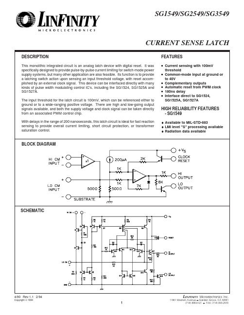
CURRENT SENSE LATCHDESCRIPTIONThis monolithic integrated circuit is an analog latch device with digital reset. It was specifically designed to provide pulse-by-pulse current limiting for switch-mode power supply systems, but many other application are also feasible. Its function is to provide a latching switch action upon sensing an input threshold voltage, with reset accom-plished by an external clock signal. This device can be interfaced directly with many kinds of pulse width modulating control IC's, including the SG1524, SG1525A and SG1527A.The input threshold for the latch circuit is 100mV, which can be referenced either to ground or to a wide-ranging positive voltage. There are high and low-going output signals available, and both the supply voltage and clock signal can be taken directly from an associated PWM control chip.With delays in the range of 200 nanoseconds, this latch circuit is ideal for fast reaction sensing to provide overall current limiting, short circuit protection, or transformer saturation control.FEATURES•Current sensing with 100mV threshold•Common-mode input at ground or to 40V•Complementary outputs •Automatic reset from PWM clock •180ns delay•Interface direct to SG1524,SG1525A, SG1527AHIGH RELIABILITY FEATURES - SG1549♦Available to MIL-STD-883♦LMI level "S" processing available ♦Radiation data availableBLOCK DIAGRAMSCHEMATICAPPLICATION NOTES (continued)FIGURE 2 — CURRENT CONTROL FOR A BUCK REGULATOR WITHCONSTANT DRIVE CURRENTFIGURE 4 — POWER BOOST AND CURRENT CONTROL WITH THE SG1627FIGURE 3 — A PUSH-PULL CONVERTER WITH LOW-LINEEMITTER CURRENT SENSINGAnother method of introducing the current shutdown signal is shown in Figure 2 where the SG1524 is used to activate a constant drive current to the high-current switch, in this case an SM600. The 2N2222 forms a constant current generator when driven from the SG1524’s 5.0 volt reference through a 1K resistor. This transistor is then switched off by the LO OUTPUT transistor in the SG1549, achieving the fastest re-sponse to the output of the regulator.LOW LINE SENSING - In many types of feed-forward or push-pull converters, current protection may be provided by sensing in an emitter resistor referenced to ground on the primary side of an output trans-former. The fast-reacting SG1549 can easily sense secondary overload as reflected back to the primary and, additionally, provide protection from unbalanced transformer saturation.When using the LO CM inputs, the HI CM inputs should be shorted together. While the LO CM inputs may be connected directly across a sense resistor, R SC , a small low-pass filter as shown in Figure 3 is often required to eliminate high frequency transients. It must be remembered that the 500Ω input impedance at the LO CM terminals will cause the use of R1 to increase the effective threshold; however, this also offers the possibility of an easily adjustable threshold by incorporating a potenti-ometer at the input.Coupling the output signal from the SG1549 to the control chip may be done in several ways including the use of either the Compensation or Shutdown pins on the SG1524 as described earlier.Another convenient way to tie the output of the SG1549 into the PWM control in higher power applications is by using the SG1627 Dual Interface Driver and connecting the LO OUTPUT terminal of the Sg1549directly to the two Non-Inverting inputs of the SG1627 as shown in Figure 4.And finally, keep in mind that the LO OUTPUT terminal of the SG1549will easily drive most high-speed optical couplers should some type of isolation between current sense and shutdown control be required.AmbientTemperature Range Part No.PackageConnection Diagram8-PIN CERAMIC DIP Y - PACKAGE87652134— HI CM INPUT + HI CM INPUT + LO CM INPUT — LO CM INPUTCLOCK RESET +V SLO OUTPUTHI OUTPUT SG1549Y/883B -55°C to 125°C SG1549Y/DESC -55°C to 125°C SG1549Y -55°C to 125°C SG2549Y -25°C to 85°C SG3549Y 0°C to 70°C CONNECTION DIAGRAMS & ORDERING INFORMATION (See Notes Below)8-PIN PLASTIC DIP M - PACKAGESG2549M -25°C to 85°C SG3549M0°C to 70°CNote 1. Contact factory for JAN and DESC product availability. 2. All parts are viewed from the top.。
w25q256jw电气参数解读
w25q256jw电气参数解读W25Q256JW是一种高性能的串行闪存器件,具有广泛的应用领域,包括数字摄像头、便携式和无线通信设备、数字音频播放器、数字音频广播、便携式电子游戏机、手持式数据采集和储存设备等。
它采用先进的闪存器件技术,具有高速读写、大容量存储以及低功耗等优点。
本文将详细解读W25Q256JW的电气参数,并分析其对应的性能特点和应用场景。
1.供电电压(VCC)W25Q256JW的供电电压范围为2.7V至3.6V,符合大部分数字电路工作电压的要求。
采用低功耗的供电电压,能够在保证稳定性的同时减少功耗,适合便携式和无线通信设备等对电池寿命有要求的应用场景。
2.闪存器件容量W25Q256JW是一种256Mb的闪存器件,也就是说它的存储容量为256兆位。
在实际应用中,通过SPI接口进行串行通信,能够以较高的速度读取和写入大容量的数据,适合数据存储和传输需求较大的应用场景。
3.时序参数W25Q256JW的时序参数包括读取时序、写入时序和擦除时序等。
在SPI接口模式下,它的最大串行时钟速度为104MHz,读取速度可达到65MB/s。
在实际应用中,通过优化时序参数和SPI接口的配置,可以实现高速的数据读写和传输,满足快速响应和高性能需求。
4.存储器排列W25Q256JW的存储器排列为512个块,每个块包含16个扇区,每个扇区包含16个子扇区。
通过SPI指令和地址控制,能够对存储器进行灵活和高效的读写操作,满足不同应用场景下的数据管理和存储需求。
5.通信接口W25Q256JW采用SPI接口进行通信,能够实现简单、高效的串行数据传输。
SPI通信协议具有灵活、可靠的特点,适合在各种数字系统中使用,包括嵌入式系统、通信设备和数字电子产品等。
6.工作温度范围W25Q256JW的工作温度范围为-40°C至85°C,适应了在各种环境条件下的使用需求。
在工业控制、汽车电子、军事航空等各种严苛的环境条件下,W25Q256JW都能够可靠地工作和稳定地传输数据。
UCQ中文资料

H -C
RoHS Hazardous Materials compliance
C = RoHS-6 (no lead), standard Y = RoHS-5 (with lead), optional, special order
ORDERING GUIDE Output R/N (mVp-p) Root Models ➀ UCQ-1.2/40-D24P-C UCQ-1.2/30-D48N-C UCQ-1.5/25-D48N-C UCQ-1.5/40-D48N-C UCQ-1.8/30-D48N-C UCQ-2.5/40-D24P-C UCQ-2.5/30-D48N-C UCQ-3.3/35-D24P-C UCQ-3.3/20-D48N-C UCQ-3.3/30-D48N-C UCQ-5/20-D24P-C UCQ-5/20-D48N-C UCQ-5/25-D48N-C UCQ-8/12-D24P-C UCQ-12/8.3-D48N-C UCQ-15/6.7-D24P-C Vout Iout Power (Volts) (Amps) (Watts) Typ. Max. Regulation (Max.) ➁ Line Load Vin Nom. (Volts) Range (Volts) Iin no load (mA) Input Iin full load (Amps) Efficiency Min. Typ.
50 50 50 100 80 50 30 50 50 50 35
100 80 100 TBD 120 100 50 80 80 60 55
Please contact Murata Power Solutions for further information. ±0.125% ±0.25% 48 36-75 30 0.90 ±0.125% ±0.25% 48 36-75 50 0.94 ±0.125% ±0.25% 48 36-75 50 1.45 ±0.125% ±0.25% 48 36-75 45 1.31 ±0.125% ±0.25% 24 18-36 120 4.96 ±0.2% ±0.25% 48 36-75 50 1.80 ±0.125% ±0.25% 24 18-36 130 5.41 ±0.125% ±0.25% 48 36-75 50 1.53 ±0.2% ±0.25% 48 36-75 50 2.3 ±0.125% ±0.25% 24 18-36 160 4.55 ±0.125% ±0.25% 48 36-75 80 2.24 Please contact Murata Power Solutions for further information.
三菱多功能电子测量仪

警报延长 时间
警报发生
最大值更新
上限值
下限值
最小值更新 0A、0V时不输出下限警报。
时间
设备启动时的便利的测试功能
在设备启动时没有电流、电压输入的状态下也应答模拟输出、脉冲输出、警报输出及通讯数据。因此可简易地进行配线及系统监控程 序的确认。
5
功能说明
LCD的功能
1
2
1 LEAD(超前)显示
2 LAG(滞后)显示
●对应DIN 96×96 尺寸 ●3P4W/3P3W 共用 ●输出选购件后装式 ●符合CE标志 ●符合欧州RoHS指令(2002/95/EC)
监控
三菱独有的ASIC给您带来 高精度的测量功能
●监控上/下限值项目达4项之多 ●谐波监控 ●测量导入/导出有功能量
显示
屏幕显示读取容易
●可显示4项项目 ●背景灯自动关闭功能
小数点位置会移动 4
便利于设备监控的上下限监控功能
●最大可上下限监控4点 在装配有ME-4201-NS96选购件的状态下,发生警报时能接点输出。 (因接点输出为1点,所以输出为被设定上下限警报项目的OR输出)
■基于LCD的上下限警报显示 可确认对应于现在值显示及最大值、最小值显示的警报发生状态。
<现在值显示画面的警报显示例>
6
■ 外形、安装、连接
23
■ 型号一览
26
■ 安全注意事项
28
概要及特长
ModBus通讯系统对应(ME96NSR-MB,选购件ME-0052-NS96)
中央监视装置
RS485/RS232 转换器
RS232
RS485(ModBus)
●最适合于PC监控的ModBus通讯系统 ●通过安装选购件ME-0052-NS96,可监控远程接点输入信号及控制接点输出信号的
K9F2G08U0M中文资料

2
元器件交易网
K9F2G08Q0M K9F2G16Q0M K9F2G08U0M K9F2G16U0M
Preliminary FLASH MEMORY
256M x 8 Bit / 128M x 16 Bit NAND Flash Memory
PRODUCT LIST
Part Number K9F2G08Q0M-Y,P K9F2G16Q0M-Y,P K9F2G08U0M-Y,P K9F2G16U0M-Y,P 2.7 ~ 3.6V Vcc Range 1.70 ~ 1.95V Organization X8 X16 X8 X16 TSOP1 PKG Type
FEATURES
• Voltage Supply -1.8V device(K9F2GXXQ0M): 1.70V~1.95V -3.3V device(K9F2GXXU0M): 2.7 V ~3.6 V • Organization - Memory Cell Array -X8 device(K9F2G08X0M) : (256M + 8,192K)bit x 8bit -X16 device(K9F2G16X0M) : (128M + 4,096K)bit x 16bit - Data Register -X8 device(K9F2G08X0M): (2K + 64)bit x8bit -X16 device(K9F2G16X0M): (1K + 32)bit x16bit - Cache Register -X8 device(K9F2G08X0M) : (2K + 64)bit x8bit -X16 device(K9F2G16X0M) : (1K + 32)bit x16bit • Automatic Program and Erase - Page Program -X8 device(K9F2G08X0M) : (2K + 64)Byte -X16 device(K9F2G16X0M) : (1K + 32)Word - Block Erase -X8 device(K9F2G08X0M) : (128K + 4K)Byte -X16 device(K9F2G16X0M) : (64K + 2K)Word • Page Read Operation - Page Size - X8 device(K9F2G08X0M) : 2K-Byte - X16 device(K9F2G16X0M) : 1K-Word - Random Read : 25µs(Max.) - Serial Access : 50ns(Min.) 30ns(Min., K9F2G08U0M only) • Fast Write Cycle Time - Page Program time : 300µs(Typ.) - Block Erase Time : 2ms(Typ.) • Command/Address/Data Multiplexed I/O Port • Hardware Data Protection - Program/Erase Lockout During Power Transitions • Reliable CMOS Floating-Gate Technology - Endurance : 100K Program/Erase Cycles - Data Retention : 10 Years • Command Register Operation • Cache Program Operation for High Performance Program • Power-On Auto-Read Operation • Intelligent Copy-Back Operation • Unique ID for Copyright Protection • Package : - K9F2GXXX0M-YCB0/YIB0 48 - Pin TSOP I (12 x 20 / 0.5 mm pitch) - K9F2GXXX0M-PCB0/PIB0 : Pb-FREE PACKAGE 48 - Pin TSOP I (12 x 20 / 0.5 mm pitch)
烟台山友电气COTEK纯正波逆变器全系列说明书 中文

150W300W逆变器型号(S150-XXX S300-XXX)输入输出完全隔离设计能快速并行启动电容、电感负载三色指示灯显示,输入电压,输出电压,负载水准和故障情形负载控制风扇冷却高级微处理控制系统设计过压/欠压/短路/过载/超温保护说明型号项目S150-112 S150-124 S150-212 S150-224 S300-112 S300-124 S300-212 S300-224 输出功率150W 300W冲击功率200W 400W输入电压12V 24V 12V 24V 12V 24V 12V 24V输入电压范围10.5-15.0 21.0-30.0 10.5-15.0 21.0-30.0 10.5-15.0 21.0-30.0 10.5-15.0 21.0-30.0 输出电压110VAC±5% 230VAC±5% 110VAC±5% 230VAC±5% 频率50/60Hz±3%瞬间效率91% 92% 90% 93% 92% 93% 91% 94% 最大效率86% 87% 85% 88% 87% 88% 86% 89% 满载效率72% 79% 72% 80% 72% 78% 72% 80% 输出电流0.18A 0.15A 0.22A 0.16A 0.26A 0.23A 0.23A 0.15A 输出波形纯正弦波(失真率<4%)可允许的功率因素cosθ-90°~cosθ+90°自动保护过压/欠压/短路/过载/超温保护远程控制外接开关远程控制安规认证UL458 EN60950EN50081-1:1992EN50082-1:1992EN55022B:1994 电磁干扰FCC Class BEN61000-4-2:1995EN61000-4-3:1996ENV50204:1995工作环境温度0℃~40℃内储温度范围-30℃to70℃冷却负载控制风扇冷却尺寸237*155*72mm/9.33*6.10*2.83英寸重量 3.5公斤/7.7磅型号(S600-XXX)纯正弦波输出(失真率<3%)输出频率、开关选择:50/60hz输入输出完全隔离设计高效率设计88~94%适应于容性、感性负载三色指示灯显示,输入电压,输出电压,负载水准和故障情形适应于冲击性负载负载控制风扇冷却高级微处理控制系统设计過壓/欠壓/短路/過載/超溫保護说明型号型号型号型号型号型号项目S600-112 S600-124 S600-148 S600-212 S600-224 S600-248 输出功率600W最大输出功率680W冲击功率800W输入电压12VDC 24VDC 48VDC 12VDC 24VDC 48VDC 输出电压100/110/120VAC+-3% 220/230/240VAC+-3% 频率50/60HZ+/-0.05%满载效率87% 90% 92% 90% 93% 94% 输出电流0.87A 0.43A 0.23A 0.83A 0.43A 0.22A 输出波形纯正弦波(失真率<3%)输出电压范围100/110/120Vrms-10%+4% 220/230/240Vrms-10%+4%输入电压范围10.5-15 21.0-30 42.0-60 10.5-15 21.0-30 42.0-60 电压,负载指示LED 红色/橙色/绿色自动保护超载,过压,欠压,超温,短路,低电池等报警保护安规认证UL458 EN60950EN50081-1:1992EN50082-1:1992EN55022B:1994EN61000-4-2:1995EN61000-4-3:1996 电磁干扰FCC Class BENV50204:1995 e-Marke13-020866 工作环境温度0~50℃℃内储温度范围-30to70℃℃冷却自动控制制冷风扇尺寸295(L)*180(W)*72(H)mm /11.61(L)*7.09(W)*2.83(H)英寸重量 2.7kgs./5.4Lbs.型号(S1500-XXX)纯正弦波输出(失真率<2%)输入输出完全隔离设计RS-232C远端电脑监控设计输入电压,负载LED指示状态自动控制制冷风扇采用微处理器控制系统设计过压/欠压/短路/过载/超温保护输出电压,频率开关选择说明型号型号型号型号型号型号项目S1500-112 S1500-124 S1500-148 S1500-212 S1500-224 S1500-248 输出功率1500W冲击功率2000W输入电压12VDC 24VDC 48VDC 12VDC 24VDC 48VDC 输出电压100/110/115/120V+—3% 200/220/230/240V+-3%频率50/60HZ+/-0.05%输出电流25A 11A满载效率85% 87% 88% 86% 89% 90% 空载损耗 1.5W Saving Mode≦输出波形纯正弦波(失真率<3%)输出电压范围100/110/115/120Vrms-10%+4% 200/220/230/240Vrms-10%+4%输入电压范围10.0-16.0 20.0-32.0 42.0-62.0 10.0-16.0 20.0-32.0 42.0-62.0 自动保护超载,过压,欠压,超温,短路,低电池等报警保护省电模式恢复时间5秒面版控制端口RS-232C远端控制器任意选择安规认证UL458 EN60950EN50081-1:1992EN50082-1:1992EN55022B:1994EN61000-4-2:1995EN61000-4-3:1996 电磁干扰FCC Class BENV50204:1995e-Marke13-020932工作环境温度0~40℃℃内储温度范围-30to70℃冷却自动控制制冷风扇尺寸390(L)*275(W)*105(H}mm/15.4(L)*10.8(W)*4.1(H)Inch 重量7.0kgs/15.5lbs.型号(SK700)纯正弦波输出(失真率<3%)输出频率、开关选择:50/60Hz输入输出完全隔离设计高效率设计89-95%适应于容性、感性负载三色指示灯显示,输入电压,输出电压,负载水准和故障情形负载控制风扇冷却高级微处理控制系统设计过压/欠压/短路/过载/超温保护说明型号型号型号型号型号型号项目SK700-112 SK700-124 SK700-148 SK700-212 SK700-224 SK700-248输出功率700W最大输出功率800W冲击功率1200W输入电压12VDC 24VDC 48VDC 12VDC 24VDC 48VDC 输出电压100/110/120VAC+-3% 220/230/240VAC+-3%频率50/60HZ+/-0.05%输出波形纯正弦波(失真率<3%)满载效率89% 91% 92% 91% 93% 94% 无负载直流损耗 1.25A 0.64A 0.31A 1.20A 0.60A 0.28A 待机直流损耗0.25A 0.15A 0.08A 0.25A 0.15A 0.08A输入电压范围10.5-15 21.0-30 42.0-60 10.5-15 21.0-30 42.0-6电压,负载指示LED 红色/橙色/绿色故障指示LED 红色自动保护超载,过压,欠压,超温,短路,低电池等报警保护安规认证UL458 EN60950EN50081-1:1992EN50082-1:1992EN55022B:1994EN61000-4-2:1995EN61000-4-3:1996 电磁干扰FCC Class BENV50204:1995 e-Mark e13-02 0866工作环境温度-10℃~50℃内储温度范围-30℃to70℃冷却负载控制冷却风扇(65℃开,45℃关)尺寸295(L)*180(W)*72(H)mm /11.61(L)*7.09(W)*2.83(H)英寸型号(SK1000)纯正弦波输出(失真率<3%)输出频率、开关选择:50/60Hz输入输出完全隔离设计高效率设计89-95%适应于容性、感性负载三色指示灯显示,输入电压,输出电压,负载水准和故障情形负载控制风扇冷却高级微处理控制系统设计过压/欠压/短路/过载/超温保护说明型号型号型号型号型号型号项目SK1000-112 SK1000-124 SK1000-148 SK1000-212 SK1000-224 SK100 0-248输出功率1000W最大输出功率1150W冲击功率2000W输入电压12VDC 24VDC 48VDC 12VDC 24VDC 48VDC 输出电压100/110/120VAC+-3% 220/230/240VAC+-3%频率50/60HZ+/-0.05%输出波形纯正弦波(失真率<3%)满载效率89% 92% 93% 91% 94% 95% 无负载直流损耗 1.43A 0.75A 0.38A 1.25A 0.65A 0.38A 待机直流损耗0.25A 0.15A 0.09A 0.25A 0.15A 0.09A输入电压范围10.5-15 21.0-30 42.0-60 10.5-15 21.0-30 42.0-6电压,负载指示LED 红色/橙色/绿色故障指示LED 红色自动保护超载,过压,欠压,超温,短路,低电池等报警保护安规认证UL458 EN60950EN50081-1:1992EN50082-1:1992EN55022B:1994EN61000-4-2:1995EN61000-4-3:1996 电磁干扰FCC Class BENV50204:1995 e-Mark e13-02 0866工作环境温度-10℃~50℃内储温度范围-30℃to70℃冷却负载控制冷却风扇(65℃开,45℃关)尺寸383(L)*182(W)*88(H)mm /15.08(L)*7.17(W)*3.46(H)英寸型号(SK1500)纯正弦波输出(失真率<3%)输出频率、开关选择:50/60Hz输入输出完全隔离设计高效率设计89-95%适应于容性、感性负载三色指示灯显示,输入电压,输出电压,负载水准和故障情形负载控制风扇冷却高级微处理控制系统设计过压/欠压/短路/过载/超温保护说明型号型号型号型号型号型号项目SK1500-112 SK1500-124 SK1500-148 SK1500-212 SK1500-224 SK150 0-248输出功率1500W最大输出功率1725W冲击功率3000W输入电压12VDC 24VDC 48VDC 12VDC 24VDC 48VDC 输出电压100/110/120VAC+-3% 220/230/240VAC+-3%频率50/60HZ+/-0.05%输出波形纯正弦波(失真率<3%)满载效率88% 91% 92% 90% 93% 94% 无负载直流损耗 1.45A 0.75A 0.40A 1.40A 0.70A 0.40A 待机直流损耗0.28A 0.15A 0.09A 0.28A 0.15A 0.09A输入电压范围10.5-15 21.0-30 42.0-60 10.5-15 21.0-30 42.0-6电压,负载指示LED 红色/橙色/绿色故障指示LED 红色自动保护超载,过压,欠压,超温,短路,低电池等报警保护安规认证UL458 EN60950EN50081-1:1992EN50082-1:1992EN55022B:1994EN61000-4-2:1995EN61000-4-3:1996 电磁干扰FCC Class BENV50204:1995 e-Mark e13-02 0866工作环境温度-10℃~50℃内储温度范围-30℃to70℃冷却负载控制冷却风扇(65℃开,45℃关)尺寸415(L)*191(W)*88(H)mm /16.34(L)*7.52(W)*3.46(H)英寸型号(SK2000)纯正弦波输出(失真率<3%)输出频率、开关选择:50/60Hz输入输出完全隔离设计高效率设计89-95%适应于容性、感性负载三色指示灯显示,输入电压,输出电压,负载水准和故障情形负载控制风扇冷却高级微处理控制系统设计过压/欠压/短路/过载/超温保护说明型号型号型号型号型号型号项目SK2000-112 SK2000-124 SK2000-148 SK2000-212 SK2000-224 SK2000 -248输出功率2000W最大输出功率2300W冲击功率4000W输入电压12VDC 24VDC 48VDC 12VDC 24VDC 48VDC 输出电压100/110/120VAC+-3% 220/230/240VAC+-3% 频率50/60HZ+/-0.05%输出波形纯正弦波(失真率<3%)满载效率89% 92% 93% 91% 94% 95% 无负载直流损耗 2.8A 1.5A 0.7A 2.8A 1.5A 0.7A 待机直流损耗0.50A 0.30A 0.16A 0.50A 0.25A 0.12A输入电压范围10.5-15 21.0-30 42.0-60 10.5-15 21.0-30 42.0-6电压,负载指示LED 红色/橙色/绿色故障指示LED 红色自动保护超载,过压,欠压,超温,短路,低电池等报警保护安规认证UL458 EN60950EN50081-1:1992EN50082-1:1992EN55022B:1994EN61000-4-2:1995EN61000-4-3:1996 电磁干扰FCC Class BENV50204:1995 e-Mark e13-02 0866工作环境温度-10℃~50℃内储温度范围-30℃to70℃冷却负载控制冷却风扇(65℃开,45℃关)尺寸422(L)*208(W)*160(H)mm /16.6(L)*8.18(W)*6.30(H)英寸型号(SK3000)纯正弦波输出(失真率<3%)输出频率、开关选择:50/60Hz输入输出完全隔离设计高效率设计89-95%适应于容性、感性负载三色指示灯显示,输入电压,输出电压,负载水准和故障情形负载控制风扇冷却高级微处理控制系统设计过压/欠压/短路/过载/超温保护说明型号型号型号型号型号型号项目SK3000-112 SK3000-124 SK3000-148 SK3000-212 SK3000-224 SK300 0-248输出功率3000W最大输出功率3450W冲击功率6000W输入电压12VDC 24VDC 48VDC 12VDC 24VDC 48VDC 输出电压100/110/120VAC+-3% 220/230/240VAC+-3%频率50/60HZ+/-0.05%输出波形纯正弦波(失真率<3%)满载效率88% 91% 92% 90% 93% 94% 无负载直流损耗 2.8A 1.5A 0.7A 2.8A 1.5A 0.7A 待机直流损耗0.55A 0.35A 0.19A 0.55A 0.35A 0.19A输入电压范围10.5-15 21.0-30 42.0-60 10.5-15 21.0-30 42.0-6电压,负载指示LED 红色/橙色/绿色故障指示LED 红色自动保护超载,过压,欠压,超温,短路,低电池等报警保护安规认证UL458 EN60950EN50081-1:1992EN50082-1:1992EN55022B:1994EN61000-4-2:1995EN61000-4-3:1996 电磁干扰FCC Class BENV50204:1995 e-Mark e13-02 0866工作环境温度-10℃~50℃内储温度范围-30℃to70℃冷却负载控制冷却风扇(65℃开,45℃关)尺寸452(L)*208(W)*166(H)mm /17.8(L)*8.18(W)*6.53(H)英寸型号(ST600-2XX□)内置10A转换开关交流电源转换灵敏适应于容性、感性负载交流电源插座和接线式双模式选择过压/欠压/短路/过载/超温保护说明型号项目ST600-212 ST600-224 输出功率600W最大输出功率680W冲击功率800W输入电压12V 24V输出电压范围、频率200/220/240V±3% 50/60Hz+/-0.05% 满载效率90.0% 93.0% 输出电流0.87A 0.43A 输出波形纯正弦波(失真率<3%)可允许的功率因素cosθ-90°~cosθ+90°输入电压范围10.5-15VDC 21.0-30VDC 电压、负载指示LED 红色/橙色/绿色电源状态LED 红色/绿色自动保护超载、过压、欠压、超温、短路、低电池等报警保护熔断电流7Amp转换开关10Amp转换时间4~8msec安规认证EN60950EN50081-1:1992EN50082-1:1992EN61000-4-3:1996 电磁干扰EN61000-4-2:1995EN55022B:1994ENV50204:1995远程控制CR-8同步交流转换工作环境温度0℃-40℃℃℃内储温度范围-30to70冷却负载控制风扇冷却尺寸11.42L*7.05W*3.15H英寸重量 3.3公斤/6.6磅正弦波逆变器安全认证机种名称安规认证编码型号:S150-*** S300-***安规认证* Meet UL458 EN60950EMC(电磁兼容)认证** FCC Class B EN50081-1:1992EN50082-1:1992EN55022B:1994EN61000-4-2:1995EN61000-4-3:1996ENV50204:1995型号:S600-*** S1500-***安规认证UL458 EN60950 EMC(电磁兼容)认证FCC Class B EN50081-1:1992e-MarkEN50082-1:1992e13-020866EN55022B:1994EN61000-4-2:1995EN61000-4-3:1996ENV50204:1995MODEL:S1000-***安规认证UL458 EN60950 EMC(电磁兼容)认证FCC Class B EN50081-1:199e-MarkEN50082-1:1992 e13-020866EN55022B:1994EN61000-4-2:1995EN61000-4-3:1996ENV50204:1995MODEL:ST600-2**EMC(电磁兼容)认证FCC Class B EN60950EN50081-1:1992EN55022B:1994EN61000-4-3:1996EN50082-1:1992EN61000-4-2:1995ENV50204:199511。
2SD2659中文资料
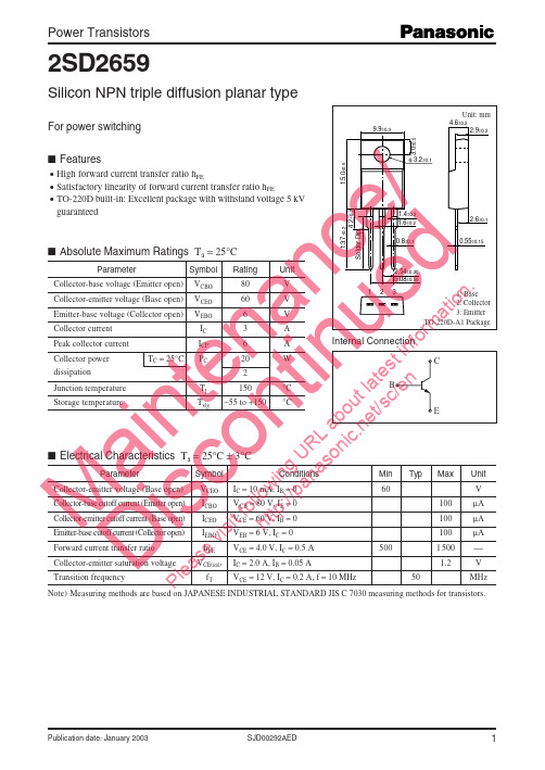
9.9±0.3
3.0±0.5
4.6±0.2 2.9±0.2
M Di ain sc te on na tin nc ue e/ d
13.7±0.2 4.2±0.2 Solder Dip
15.0±0.5
φ 3.2±0.1
1.4±0.2 1.6±0.2
2.6±0.1
■ Absolute Maximum Ratings Ta = 25°C
100
Safe operation area
Non repetitive pulse TC = 25°C
Collector power dissipation PC (W)
30 25 (1) 20 15 10 5 0
(1) TC = Ta (2) Without heat sink PC = 2 W
IC = 10 mA, IB = 0
Collector-base cutoff current (Emitter open)
VCB = 80 V, IE = 0 VCE = 60 V, IB = 0 VEB = 6 V, IC = 0
Collector-emitter cutoff current (Base open) Emitter-base cutoff current (Collector open) Forward current transfer ratio
Parameter Symbol VCEO ICBO ICEO IEBO hFE fT Collector-emitter voltage (Base open)
Conditions
Min 60
or m
Typ 50
1: Base 2: Collector 3: Emitter TO-220D-A1 Package
G941T25U中文资料
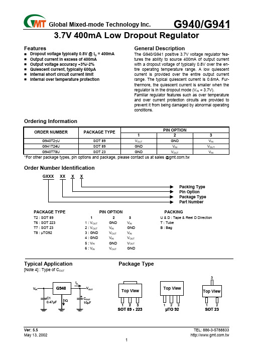
3.7V 400mA Low Dropout RegulatorFeaturesDropout voltage typically 0.8V @ I O = 400mA Output current in excess of 400mA Output voltage accuracy +3%/-2% Quiescent current, typically 600µA Internal short circuit current limit Internal over temperature protectionGeneral DescriptionThe G940/G941 positive 3.7V voltage regulator fea-tures the ability to source 400mA of output current with a dropout voltage of typically 0.8V over the en-tire operating temperature range. A low quiescent current is provided over the entire output current range. The typical quiescent current is 0.6mA. Fur-thermore, the quiescent current is smaller when the regulator is in the dropout mode (V IN < 3.7V).Familiar regulator features such as over temperature and over current protection circuits are provided to prevent it from being damaged by abnormal operating conditions.Ordering InformationPIN OPTIONORDER NUMBERPACKAGE TYPE1 2 3G940T21U SOT 89 V OUT GND V IN G941T24U SOT 89 GND V IN V OUT G940T73U SOT 23 GND V OUT V IN*For other package types, pin options and package, please contact us at sales @ Order Number IdentificationType Pin Option TypePart NumberPACKAGE TYPEPIN OPTIONPACKINGT2 : SOT 89 1 2 3U & D : Tape & Reel D DirectionT6 : SOT 223 1 : V OUT GNDV IN T : Tube T7 : SOT 23 2 : V OUTV INGND B : Bag T8 : µTO92 3 : GND V OUT V IN4 : GND V INV OUT 5 : V IN GNDV OUT6 : V IN V OUT GNDTypical Application Package Type[Note 4] : Type of C OUTSOT 893µTO 92SOT 23、223V OUTAbsolute Maximum Ratings (Note 1)Input Voltage……………………………..……..…..…10V Power Dissipation Internally Limited ..(Note 2) Maximum Junction Temperature………….….…...150°C Storage Temperature Range…..…..…..-65°C ≤ T J ≤+150°C Lead Temperature, Time for Wave SolderingSOT 89, SOT23 Package….….…..……..…....260°C, 4s Continuous Power Dissipation (T A = + 25°C)SOT 23(1)…….…………………….….……….……...0.3W SOT 89(1)……………………….………..………..…0.42WNote (1): See Recommended Minimum Footprint.Operating Conditions (Note 1)Input Voltage………………………….…………….4V~7V Temperature Range………………….…0°C ≤ T J ≤125°CElectrical CharacteristicsV IN =5V, I O = 400mA, C IN = 1 µF, C OUT =10 µF, All specifications apply for T A = T J = 25°C. [Note 3]PARAMETER CONDITIONS MIN TYP MAX UNITSOutput Voltage Accuracy I O = 10mA -2 - +3 % Line Regulation V IN = 4V to 7V, I O = 50mA - 0.08 0.9 %/V Load Regulation I O = 10mA to 400mA - - 2.2 % Output Impedance 100mA DC and 100mA AC, fo = 120Hz - 100 - m ΩQuiescent Current V IN =5V - 0.6 - mA Ripple Rejection f i = 120 Hz, 1V P-P , Io = 100mA - 42 - dBI O = 400mA - 0.8 0.9 V Dropout Voltage I O = 100mA - 130 150 mV Short Circuit Current-0.76-AOver Temperature- 125 - °CNote 1: Absolute Maximum Ratings are limits beyond which damage to the device may occur. Operating Condi-tions are conditions under which the device functions but the specifications might not be guaranteed. For guaranteed specifications and test conditions see the Electrical Characteristics.Note 2: The maximum power dissipation is a function of the maximum junction temperature, T Jmax ; total thermal re-sistance, θJA , and ambient temperature T A . The maximum allowable power dissipation at any ambient tem-perature is T jmax -T A / θJA . If this dissipation is exceeded, the die temperature will rise above 130°C and ICwill go into thermal shutdown. For the G940/G941 in SOT 23 package, θJA is 350°C/W and in the SOT 89 package is 250°C/W (See Recommend Minimum Footprint). The safe operation in SOT 23 & SOT 89 package, it can see “Typical Performance Characteristics” (Safe Operating Area).Note3: Low duty pulse techniques are used during test to maintain junction temperature as close to ambient aspossible.Note4: The type of output capacitor should be tantalum or aluminum.DefinitionsDropout VoltageThe input/output Voltage differential at which the regulator output no longer maintains regulation against further reductions in input voltage. Measured when the output drops 100mV below its nominal value, dropout voltage is affected by junction temperature, load cur-rent and minimum input supply requirements.Line RegulationThe change in output voltage for a change in input voltage. The measurement is made under conditions of low dissipation or by using pulse techniques such that average chip temperature is not significantly af-fected.Load RegulationThe change in output voltage for a change in load current at constant chip temperature. The measure-ment is made under conditions of low dissipation or by using pulse techniques such that average chip tem-perature is not significantly affected.Maximum Power DissipationThe maximum total device dissipation for which the regulator will operate within specifications.Quiescent Bias CurrentCurrent which is used to operate the regulator chip and is not delivered to the load.Typical Performance Characteristics(V IN =5V, C IN =1µF, C OUT =10µF, T A =25°C, unless otherwise noted.)Ch1: Vout (offset=3.70V)Ch1: Iout (400mA/div)Ch2: Vin (offset=5.0V)Ch2: Vout (offset=3.70V)Iout=100mAGround Current vs. Load CurrentLine TransientLoad TransientOutput Voltage Accuracy vs. Load CurrentDropout Voltage vs. Load CurrentRecommend Minimum FootprintNote: V IN(max) <= 6.5VNote: V IN(max)<= 6.5VPackage InformationSOT-89 (T2) PackageDIMENSIONS IN MILLIMETERS DIMENSIONS IN INCHESSYMBOLSMIN NOM MAX MIN NOM MAXA 1.40 1.50 1.60 0.055 0.059 0.063 A1 0.80 1.04 ----- 0.031 0.041 ----- b 0.36 0.42 0.48 0.014 0.0160.048 b1 0.41 0.47 0.53 0.016 0.018 0.020 C 038 0.40 0.43 0.014 0.015 0.017 D 4.40 4.50 4.60 0.173 0.177 0.181 D1 1.40 1.60 1.75 0.055 0.062 0.069 HE ----- ----- 4.25 ----- ----- 0.167 E 2.40 2.50 2.60 0.094 0.098 0.102 e 2.90 3.00 3.10 0.114 0.118 0.122SOT-223 (T6) PackageMILLIMETERS INCHES SYMBOLSMIN MAX MIN MAXA 1.551.80 0.061 0.071 A1 0.02 0.12 0.0008 0.0047 B 0.60 0.80 0.024 0.031 B12.903.10 0.114 0.122 C 0.240.32 0.009 0.013 D 6.30 6.70 0.248 0.264 E 3.30 3.70 0.130 0.146 e 2.30 BSC0.090 BSC e1 4.60 BSC 0.181 BSC H 6.70 7.30 0.264 0.287 L 0.90 MIN0.036 MINL2 0.06 BSC 0.0024 BSCα0º 10º 0º 10º13°(4X)α(4X)SOT-23 (T7) PackageNote:1.Package body sizes exclude mold flash protrusions or gate burrs2.Tolerance ±0.1000 mm (4mil) unless otherwise specified3.Coplanarity: 0.1000mm4.Dimension L is measured in gage planeDIMENSIONS IN MILLIMETERSSYMBOLSMIN NOM MAXA 1.00 1.10 1.30 A10.00 ----- 0.10 A2 0.70 0.80 0.90 b 0.35 0.40 0.50 C 0.10 0.150.25 D 2.70 2.90 3.10 E 1.40 1.60 1.80 e ----- 1.90(TYP)----- H 2.60 2.80 3.00 L 0.37 ------ ----- θ1 1º 5º 9ºGMT Inc. does not assume any responsibility for use of any circuitry described, no circuit patent licenses are implied and GMT Inc. reserves the right at any time without notice to change said circuitry and specifications.SOT 23 Package OrientationSOT 89、223 Package Orientation。
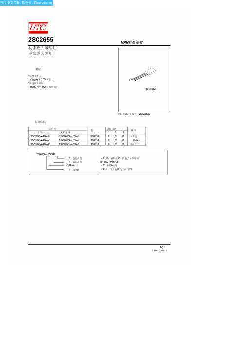
2SC2655-Y-T9N-R中文资料(Unisonic Technologies)中文数据手册「EasyDatasheet - 矽搜」
4 of 4
RUZ-092424中文资料

40 20 0
121515 241515
Efficiency %
20 0
0%
20%
40%
60%
80%
100%
0%
20%
40%
60%
80%
100%
Total Output current (%)
Total Output current (%)
Deviation / Load
25.000 20.000 25.000 20.000
元器件交易网
Features
Unregulated Converters
● ● ● ● ● ● ● ●
Dual Output from a Single Input Rail Input/Output Isolation 1kVDC Output/Output Isolation 1kVDC Power Sharing on Outputs UL94V-0 Package Material Toroidal Magnetics No Extern. Components Required Efficiency to 85%
ECONOLINE
DC/DC-Converter
RUZ Series
Selection Guide
Part Number SIP 7 RUZ-xx3.33.3 RUZ-xx0505 RUZ-xx0509 RUZ-xx0512 RUZ-xx0515 RUZ-xx0909 RUZ-xx1212 RUZ-xx1515 RUZ-xx2424 xx = Input Voltage Input Voltage (VDC) 5, 9, 12, 24 5, 9, 12, 24 5, 9, 12, 24 5, 9, 12, 24 5, 9, 12, 24 5, 9, 12, 24 5, 9, 12, 24 5, 9, 12, 24 5, 9, 12, 24 Output Voltage (V1VDC) 3.3 5 5 5 5 9 12 15 24 Output Voltage (V2VDC) 3.3 5 9 12 15 9 12 15 24 Output Current (mA) 303/303 200/200 200/111 200/84 200/66 111/111 84/84 66/66 42/42 Efficiency (%) 70 70-82 70-82 70-82 70-82 82-84 82-84 82-84 80-85
更多难得资料请到江南家电维修论坛下载!
一:机芯介绍机芯功能介绍在功能上可以实现模拟PAL制式电视信号的60HZ逐行、100HZ两种扫描模式,高清信号可以显示1080P/60,1080I/60,1080I/50,720P/60和逐行DVD 信号(图像)。
VGA方式支持640*480/60 800*600/60 1024*768/60三种模式。
产品外观介绍HDP2433为33系列外观二、机芯概述HDP2433机芯是采用华亚公司的芯片HTV180单芯片的视频处理方案,HTV180集成了ADC ,解码器,OSD 产生器,行场频转换处理芯片以及CPU 。
采用了东芝的TB1306,其功能是预视放、行场激励输出、EW 输出、EHT 、ABL 。
解码板板号是RSAG7.820.947A 。
主板是RSAG7.820.983,主板伴音切换芯片采用HEF4052BP ,伴音功放电路为ST 的TFA9842AJ ,其功能是3路声音输入,总线用两个I/O 口控制切换实现一路输出到伴音功放芯片TFA9842AJ ,总线用一路PWM 控制TFA9842AJ 的VOLUME 脚(7脚)实现音量控制。
视放板板号RSAG7.820.954,采用美国国家半导体的LM2451视放电路。
更多难得资料请到江南家电维修论坛下载!三、原理说明电源部分1:电源框图电源部分工作原理介绍本电源控制芯片采用FAIRCHILD公司的开关电源集成电路FSCQ1265,这是一种内置功率MOSFET和控制器的回扫型开关电源集成电路,且具有过流、过压、过热保护电路。
交流220V经过整流、稳压后提供给开关变压器T501,开关变压器共有5路输出:+B(130V)、+15V、+17V和+8V,10V。
+17V输出开关变压器16脚输出经整流后给N601(TFA9842AJ)第9脚提供电压+10V输出:通过变压器14脚整流输出10V给7805给解码板CPU供电5V-1,给光藕提供参考电压。
+8V输出:通过变压器18脚整流输出8V给3852调制5V 给解码板供电5V-2。
BD7956FS中文资料

United Kingdom / London TEL : +44(1)908-282-666 France / Paris China / Hong Kong Shanghai Dilian Beijing Taiwan / Taipei Korea / Seoul Singapore Malaysia / Kuala Lumpur Philippines / Manila Thailand / Bangkok
TEL : +33(0)1 56 97 30 60 FAX : +33(0) 1 56 97 30 80 TEL : +852(2)740-6262 TEL : +86(21)6279-2727 TEL : +86(411)8230-8549 TEL : +86(10)8525-2483 TEL : +866(2)2500-6956 TEL : +82(2)8182-700 TEL : +65-6332-2322 TEL : +60(3)7958-8355 TEL : +63(2)807-6872 TEL : +66(2)254-4890 FAX : +852(2)375-8971 FAX : +86(21)6247-2066 FAX : +86(411)8230-8537 FAX : +86(10)8525-2489 FAX : +866(2)2503-2869 FAX : +82(2)8182-715 FAX : +65-6332-5662 FAX : +60(3)7958-8377 FAX : +63(2)809-1422 FAX : +66(2)256-6334
EB-9V Battery-powered Automatic Flashing Module Us

KUTAI ELECTRONICS INDUSTRY CO., LTD.TEL : +886-7-8121771FAX : +886-7-8121775Website : Headquarters : No.3, Ln. 201, Qianfu St., Qianzhen Dist., Kaohsiung City 806037, TaiwanEB-9VBattery-powered Automatic Flashing ModuleUser Manual※Lithium Battery Not IncludedSECTION 1 : FEATURES●No external battery or DC power supply required, excitation power provided by an internal battery.●Small size, light weight and easy installation saving labor.●Automatic excitation detection requires no manual operation or settings.●Very low static power consumption, Up to 3 years between battery replacement in standby mode.●Excitation function repeats 3 times and stops automatically when voltage is established.●Battery low voltage indicator reminds user to change battery.●Up to three repeat flashing attempts and will automatically stop when voltage builds up.●Excitation failure indicator. Resets automatically when voltage builds up or engine is stopped.●Battery reverse polarity protection.●Excitation field F+, F- Reverse Polarity Protection.●Built in manual forced excitation push button.SECTION 2 : SPECIFICATIONSensing Voltage Input Lithium Battery SpecificationsVoltage 1 300 Vac 1 phase 2 wire Model no. Ultralife U9VL-J-PFrequency 50/60 Hz Voltage 9 VdcCurrent Normal discharge 700 mA Max Excitation Output Pulse discharge 1050 mA MaxVoltage 9 Vdc Capacity 1200 mAh @ 23 ˚CCurrent 700 mA Max.Service Life 10 yearsFlashing Output Conditions EnvironmentWhen voltage less than 10 Vac at frequency greater Operating Temperature -20 to +60 ˚Cthan 40 Hz Storage Temperature -40 to +60 ˚CRelative Humidity Max. 95%Flashing Output Time Vibration 5 Gs @ 60 HzExcitation output 5 seconds. Up to 3 attempts at 5second intervals Dimensions87.0 (L) x 41.5 (W) x 61.7 (H) mmTime Between Battery Change 3.42 (L) x 1.63 (W) x 2.43 (H) inch3 years Max. Weight( Use only Ultralife U9VL-J-P lithium battery ) 85 g +/- 2%0.19 lb +/- 2%___________________________________________________________________________________________ 2EB-9V___________________________________________________________________________________________ EB-9V3SECTION 3 : Explanation of Terminals, Indicators, and AdjustmentsSECTION 4 : Dimensions / Connection DiagramB AExternal DimensionsConnection Diagram※ Appearance and specifications of products are subject to change for improvement without prior notice.Low DC :Battery Voltage Low (red) Blinks every 5 sec when battery voltage lowPower :Power indicator (green)Blinks every 5 sec in standby modeIlluminates continuously during excitation output F+、F-:Excitation OutputConnects to generator excitation field Sensing Voltage input :1 300 VacMounting Holes * 2Manual :Manual forced excitation push button Pressing this button forces excitation output※ Both Power and Low DC indicators will blink when excitation fails。
UDQ2596A中文资料
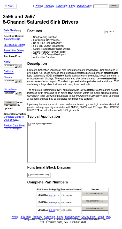
2596 and 25978-Channel Saturated Sink Drivers| Home | Products | Corporate | Sales | Design Center | AllegroMicroSystem SearchData Sheet (PDF)Selection Guides:Automotive ICs ,LED Display Drivers, Power Sink DriversPurchase From:Arrow :Bell MicroNewark :Nu Horizons : when this product is updated General Information:Complete Guide to Data Sheets (PDF)Product Data SheetClassifications (PDF)UDN2596A go UDN2596A go UDN2596A go Notify meFeatures ?Non -Inverting Function ?Low Output ON Voltages ?Up to 1.0 A Sink Capability ?50 V Min. Output Breakdown ?Output Transient -Suppression Diodes ?Output Pull -Down for Fast Turn -Off ?TTL, CMOS Compatible Inputs ?Automotive Capable DescriptionLow output -saturation voltages at high load currents are provided by UDN2596A and UDN2sink driver ICs. These devices can be used as interface buffers between standard low -power digital logic (particularly MOS) and high -power loads such as relays, solenoids, stepping motors, and or incandescent displays. The eight saturated sink drivers in each device feature high -voltage, high -current open -collector outputs. Transient suppression clamp diodes and a minimum 35 V ou sustaining voltage allow their use with many inductive loads.The saturated (non -Darlington) NPN outputs provide low collector -emitter voltage drops as well as improved turn -off times due to an active pull -down function within the output predrive section. Th UDN2596A is for use with output loads to 500 mA while the UDN2597A is for use with loaA. Adjacent outputs may be paralleled for higher load currents.Inputs require very low input current and are activated by a low logic level consistent with greater sinking capability associated with NMOS, CMOS, and TTL logic. The UDN2596A UDN2597A are rated for use with 5 V logic levels. Typical ApplicationFunctional Block DiagramComplete Part NumbersPin-Out 2596 Typical ApplicationsFunctional Block DiagramPart NumberPackage Type Temperature CommentsSamples UDN2596A DIP -20 (PDF)-20°C to 85°C request samples >>UDQ2596A DIP -20 (PDF)-40°C to 85°C request samples >>UDN2597A DIP -20 (PDF)-20°C to 85°C request samples >>Home | Site Map | Products | Corporate | Sales | Design Center | On -Line Store | Legal | HelpAllegro MicroSystems, Inc., 115 Northeast Cutoff, Worcester, MA 01606 USA,TEL: 1.508.853.5000, FAX: 1.508.853.7861。
埃森普 EAM254L 电阻断路器说明书
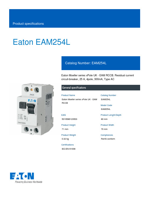
Eaton EAM254LEaton Moeller series xPole UK - EAM RCCB. Residual current circuit-breaker, 25 A, 4pole, 300mA, Type ACGeneral specificationsEaton Moeller series xPole UK - EAM RCCBEAM254L EAM254L501958612350380 mm 71 mm 70 mm 0.32 kg RoHS conformIEC/EN 61008Product NameCatalog Number Model Code EANProduct Length/Depth Product Height Product Width Product Weight Compliances CertificationsSwitchgear for residential and commercial applications Four-poleNon-delayed25 A10 kA300 mAAC current sensitivePartly surge-proof 250 A 230 V AC / 400 V AC400 V440 V4 kV0.3 A0.3 A50 Hz63 A (max. admissible back-up fuse) AC500 A25 A gG/gL10 kA0.25 kA196 V AC - 456 V AC24000 operationsApplicationNumber of polesTripping timeAmperage RatingRated short-circuit strength Fault current rating Sensitivity typeImpulse withstand current Type Voltage ratingRated operational voltage (Ue) - maxRated insulation voltage (Ui)Rated impulse withstand voltage (Uimp) Rated fault current - minRated fault current - maxFrequency ratingShort-circuit ratingLeakage current typeRated residual making and breaking capacity Admissible back-up fuse overload - max Rated short-time withstand current (Icw) Surge current capacityTest circuit rangePollution degreeLifespan, electricalEAMResidual current circuit breakersType AC45 mm470 mm (4 SU)70.5 mmDIN railIEC/EN 60715 top-hat railIP20IP40, IP54 (with moisture-proof enclosure)Box clamp1.5 mm² - 35 mm²1.5 mm²35 mm²1.5 mm²16 mm²Finger and hand touch safe, DGUV VS3, EN 50274 0.8 mm - 2 mm20000 operations-35 °C60 °C 25 A0 W1.3 W0 W0 W-25 °C55 °CMeets the product standard's requirements.Meets the product standard's requirements.Meets the product standard's requirements.Meets the product standard's requirements.Meets the product standard's requirements.Does not apply, since the entire switchgear needs to be evaluated.Does not apply, since the entire switchgear needs to be evaluated.Meets the product standard's requirements.Does not apply, since the entire switchgear needs to beFrameWidth in number of modular spacingsBuilt-in width (number of units)Built-in depthMounting MethodDegree of protectionTerminals (top and bottom)Terminal capacity (solid wire)Connectable conductor cross section (solid-core) - min Connectable conductor cross section (solid-core) - max Connectable conductor cross section (multi-wired) - min Connectable conductor cross section (multi-wired) - max Terminal protectionBusbar material thicknessLifespan, mechanicalPermitted storage and transport temperature - min Permitted storage and transport temperature - max Climatic proofing Rated operational current for specified heat dissipation (In) Heat dissipation per pole, current-dependentEquipment heat dissipation, current-dependentStatic heat dissipation, non-current-dependentHeat dissipation capacityAmbient operating temperature - minAmbient operating temperature - max10.2.2 Corrosion resistance10.2.3.1 Verification of thermal stability of enclosures10.2.3.2 Verification of resistance of insulating materials to normal heat10.2.3.3 Resist. of insul. mat. to abnormal heat/fire by internal elect. effects10.2.4 Resistance to ultra-violet (UV) radiation10.2.5 Lifting10.2.6 Mechanical impact10.2.7 Inscriptions10.3 Degree of protection of assemblies25-55 °C / 90-95% relative humidity according to IEC 60068-2evaluated.Meets the product standard's requirements.Does not apply, since the entire switchgear needs to be evaluated.Does not apply, since the entire switchgear needs to be evaluated.Is the panel builder's responsibility.Is the panel builder's responsibility.Is the panel builder's responsibility.Is the panel builder's responsibility.Is the panel builder's responsibility.The panel builder is responsible for the temperature rise calculation. Eaton will provide heat dissipation data for the devices.Is the panel builder's responsibility. The specifications for the switchgear must be observed.Is the panel builder's responsibility. The specifications for the switchgear must be observed.The device meets the requirements, provided the information in the instruction leaflet (IL) is observed.Residual current circuit breaker Additional equipment possible eaton-rcd-application-guide-br019003en-en-us.pdf eaton-protective-devices-catalog-ca20190603-en-us.pdf10.4 Clearances and creepage distances 10.5 Protection against electric shock10.6 Incorporation of switching devices and components 10.7 Internal electrical circuits and connections 10.8 Connections for external conductors 10.9.2 Power-frequency electric strength 10.9.3 Impulse withstand voltage 10.9.4 Testing of enclosures made of insulating material 10.10 Temperature rise10.11 Short-circuit rating10.12 Electromagnetic compatibility10.13 Mechanical functionFeaturesFitted with:Application notesCataloguesEaton Corporation plc Eaton House30 Pembroke Road Dublin 4, Ireland © 2023 Eaton. All rights reserved. Eaton is a registered trademark.All other trademarks areproperty of their respectiveowners./socialmediaInterlocking deviceMaximum operating temperature is 55 °C: Starting at 40 °C, the max. permissible continuous current decreases by 3% for every 1 °CEAMResidual current circuit breakersType AC eaton-xpole-accessories-ca019015en-en-us.pdfDA-DC-03_EAM03_EAM_181019DA-DC-03_EAM_020616Special featuresUsed withCertification reports。
UDQ2549资料
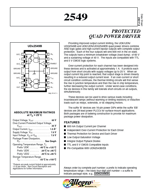
Data Sheet2549PROTECTEDQUAD POWER DRIVER115 Northeast Cutoff, Box 15036Worcester, Massachusetts 01615-0036 (508) 853-5000UDx2549EB106420A L L O W A B L E P A C K A G E P O W E R D I S S I P A T I O N I N W A T T STEMPERATURE IN °C8Dwg. GP-004-1AGROUNDGROUNDGROUND GROUNDDwg. PP-019-1KN O C O N N E C T I O NE N A B L ES U P P L Y O U T 1O U T 2O U T 3O U T 4I N 4I N 3I N 2I N 1N OC O N N E C T I O NKCopyright © 1991, 1995, Allegro MicroSystems, Inc.2549PROTECTEDQUAD POWER DRIVERCharacteristicSymbol Test ConditionsMin.Typ.Max.Units Output Leakage CurrentI CEXV OUT = 60 V, V IN = 0.8 V, V EN = 2.0 V —<1.0100µA V OUT = 60 V, V IN = 2.0 V, V EN = 0.8 V—<1.0100µA Output Sustaining Voltage V OUT(SUS)I OUT = 100 mA, V IN = V EN = 0.8 V 40——V Output Saturation VoltageV OUT(SAT)I OUT = 100 mA ——200mV I OUT = 400 mA ——400mV I OUT = 600 mA——600mV Over-Current Trip I TRIP — 1.0—A Input VoltageLogic 1V IN(1) or V EN(1) 2.0——V Logic 0V IN(0) or V EN(0)——0.8V Input CurrentLogic 1V IN(1) or V EN(1) = 2.0 V ——10µA Logic 0V IN(0) or V EN(0) = 0.8 V——-10µA Total Supply CurrentI CCI OUT = 600 mA, V IN * = V EN = 2.0 V ——65mA All Outputs OFF——15mA Clamp Diode Forward Voltage V F I F = 1.0 A—— 1.7V Clamp Diode Leakage Current I R V R = 60 V, D 1 + D 2 or D 3 + D 4——50µA Thermal LimitT J—165—°CLimitsTypical Data is for design information only.Negative current is defined as coming out of (sourcing) the specified terminal.As used here, -100 is defined as greater than +10 (absolute magnitude convention) and the minimum is implicitly zero.* All inputs simultaneously, all other tests are performed with each input tested separately.ELECTRICAL CHARACTERISTICS at T A = +25°C (prefix ‘UDN’) or over operating temperature range (prefix ‘UDK’ or ‘UDQ’), V CC = 4.75 V to 5.25 V2549PROTECTEDQUAD POWER DRIVER115 Northeast Cutoff, Box 15036Worcester, Massachusetts 01615-0036 (508) 853-5000CIRCUIT DESCRIPTION AND APPLICATIONINCANDESCENT LAMP DRIVERHigh incandescent lamp turn-ON/in-rush currents can contribute to poor lamp reliability and destroy semiconductor lamp drivers. Warming or current-limiting resistors protect both driver and lamp but use signifi-cant power either when the lamp is OFF or when the lamp is ON,respectively. Lamps with steady-state current ratings up to 600 mA can be driven by these devices without the need for warming (parallel)or current-limiting (series) resistors.When an incandescent lamp is initially turned ON, the cold filament is at minimum resistance and would normally allow a 10x to 12x in-rush current. With the these drivers, during turn-ON, the high in-rush current is sensed by the internal low-value sense resistor. Drive current to the output stage is then diverted by the shunting transistor, and the load current is momentarily limited to approximately 1.0 A. During this short transition period, the output current is reduced to a value dependent on supply voltage and filament resistance. During lamp warmup, the filament resistance increases to its maximum value, the output stage goes into saturation and applies maximum rated voltage to the lamp.INDUCTIVE LOAD DRIVERBifilar (unipolar) stepper motors, relays, or solenoids can be driven directly. The internal flyback diodes prevent damage to the output transistors by suppressing the high-voltage spikes which occur when turning OFF an inductive load. For rapid current decay (fast turn-OFF speeds), the use of Zener diodes will raise the flyback voltage andimprove performance. However, the peak voltage must not exceed the specified minimum sustaining voltage (V SUPPLY + V Z + V F ≤ V OUT(SUS)).FAULT CONDITIONSIn the event of a shorted load, the load current will attempt toincrease. As described above, the drive current to the affected output stage is reduced, causing the output stage to go linear, limiting the peak output current to approximately 1 A. As the power dissipation of that output stage increases, a thermal gradient sensing circuit will become operational, further decreasing the drive current to the affected output stage and reducing the output current to a value dependent on supply voltage and load resistance.Continuous or multiple overload conditions causing the chip tem-perature to reach approximately 165°C will result in an additional reduction in output current to maintain a safe level.If the fault condition is corrected, the output stage will return to its normal saturated condition.TYPICAL OUTPUT CHARACTERISTICDwg. GP-013O U T P U T V O L T A G E , V O U TOUTPUT CURRENT, IOUTTYPICAL OUTPUT BEHAVIORTIMEDwg. WP-008L A M P C U R R E N T2549PROTECTED QUAD POWER DRIVER UDN2549B and UDQ2549B Dimensions in Inches(controlling dimensions)Dimensions in Millimeters(for reference only)NOTES:1.Exact body and lead configuration at vendor’s option within limits shown.2.Lead spacing tolerance is non-cumulative3.Lead thickness is measured at seating plane or below.4.Webbed lead frame. Leads 4, 5, 12, and 13 are internally one piece.Dwg. MA-001-17A mm18Dwg. MA-001-17A in16182549PROTECTEDQUAD POWER DRIVER115 Northeast Cutoff, Box 15036Worcester, Massachusetts 01615-0036 (508) 853-5000UDN2549EB and UDQ2549EBDimensions in Inches (controlling dimensions)Dimensions in Millimeters (for reference only)NOTES:1.Exact body and lead configuration at vendor ’s option within limits shown.2.Lead spacing tolerance is non-cumulative3.Webbed lead frame. Leads 5 through 11 and 19 through 25 are internally one piece.Dwg. MA-005-28A in5Dwg. MA-005-28A mm52549PROTECTED QUAD POWER DRIVERThe products described here are manufactured under one or more U.S. patents or U.S. patents pending.Allegro MicroSystems, Inc. reserves the right to make, from time to time, such departures from the detail specifications as may be required to permit improvements in the performance, reliability, or manufacturability of its products. Before placing an order, the user is cautioned to verify that the information being relied upon is current.Allegro products are not authorized for use as critical components in life-support devices or systems without express written approval.The information included herein is believed to be accurate and reliable. However, Allegro MicroSystems, Inc. assumes no responsi-bility for its use; nor for any infringement of patents or other rights of third parties which may result from its use.2549PROTECTEDQUAD POWER DRIVER115 Northeast Cutoff, Box 15036Worcester, Massachusetts 01615-0036 (508) 853-5000POWER SINK DRIVERSIN ORDER OF 1) OUTPUT CURRENT, 2) OUTPUT VOLTAGE, 3) NUMBER OF DRIVERSOutput Ratings *Features Serial Latched Diode Internal mAV #Input DriversClampOutputsProtectionPart Number†75178X X –constant current –62751716X X –constant current –627610020 8–––saturated –25953032X X –––58334032X X –saturated –583250 8addressable decoder/driver DMOS –6B25950 8–X –DMOS –6B27350 8X X –DMOS –6B59525050 8addressable decoder/driver DMOS –625950 8–X –DMOS –627350 8X X –DMOS –6595135 7––X ––700330045 1–Hall sensor/driver X –X 514050 7––X ––200350 8––X ––280350 8––X saturated –259660 4––X saturated X 255795 7––X ––202395 8––X ––282335050 4–X X ––580050 7––X ––200450 8––X ––280450 8–X X ––580150 8X X –––582150 8X X X ––584150 8addressable decoder/driver DMOS –6A25950 8X X –DMOS –6A59580 8X X –––582280 8X X X ––584295 7––X ––202495 8––X ––28244503028dual 4- to 14-line decoder/driver ––681760060 4–––saturated X 254760 4––X saturated X 254970060 4––X saturated X 2543 and 255975050 8––X saturated –259790014 2–Hall sensor/driver X saturated X 362526 2–Hall sensor/driver X saturated X 3626100046 4stepper motor controller/driver MOS –7024 and 7029120046 4microstepping controller/driver MOS –7042125050 4stepper motor translator/driver –X 580450 4––X ––2064 and 2068150080 4––X ––2065 and 2069180050 4––X ––254450 4––X ––2540300046 4stepper motor controller/driver MOS –702646 4microstepping controller/driver MOS –7044400050 4––X ––287880 4––X ––2879*Current is maximum specified test condition, voltage is maximum rating. See specification for sustaining voltage limits orover-current protection voltage limits.†Complete part number includes additional characters to indicate operating temperature range and package style.。
US2 42CF35AJ 42DP 定义目的电感式接触器数据表说明书
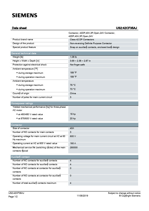
0
contacts
Number of NO contacts at contactor for auxiliary
0
contacts
Number of total auxiliary contacts maximum
4
US2:42CF35AJ Page 1/2
11/05/2019
Subject to change without notice © Copyright Siemens
vertical Surface mounting and installation Box lug
40 ... 40 lbf·in 4 AWG
Box lug
4 AWG
Quick connects, Screw-type terminals Quick Connects, Screw-type terminals
General technical data Weight [lb] Height x Width x Depth [in] Protection against electrical shock Ambient temperature [°F] ● during storage maximum ● during operation maximum Ambient temperature ● during storage maximum ● during operation maximum Country of origin Number of poles for main current circuit
- 1、下载文档前请自行甄别文档内容的完整性,平台不提供额外的编辑、内容补充、找答案等附加服务。
- 2、"仅部分预览"的文档,不可在线预览部分如存在完整性等问题,可反馈申请退款(可完整预览的文档不适用该条件!)。
- 3、如文档侵犯您的权益,请联系客服反馈,我们会尽快为您处理(人工客服工作时间:9:00-18:30)。
Data Sheet2549PROTECTEDQUAD POWER DRIVER115 Northeast Cutoff, Box 15036Worcester, Massachusetts 01615-0036 (508) 853-5000UDx2549EB106420A L L O W A B L E P A C K A G E P O W E R D I S S I P A T I O N I N W A T T STEMPERATURE IN °C8Dwg. GP-004-1AGROUNDGROUNDGROUND GROUNDDwg. PP-019-1KN O C O N N E C T I O NE N A B L ES U P P L Y O U T 1O U T 2O U T 3O U T 4I N 4I N 3I N 2I N 1N OC O N N E C T I O NKCopyright © 1991, 1995, Allegro MicroSystems, Inc.2549PROTECTEDQUAD POWER DRIVERCharacteristicSymbol Test ConditionsMin.Typ.Max.Units Output Leakage CurrentI CEXV OUT = 60 V, V IN = 0.8 V, V EN = 2.0 V —<1.0100µA V OUT = 60 V, V IN = 2.0 V, V EN = 0.8 V—<1.0100µA Output Sustaining Voltage V OUT(SUS)I OUT = 100 mA, V IN = V EN = 0.8 V 40——V Output Saturation VoltageV OUT(SAT)I OUT = 100 mA ——200mV I OUT = 400 mA ——400mV I OUT = 600 mA——600mV Over-Current Trip I TRIP — 1.0—A Input VoltageLogic 1V IN(1) or V EN(1) 2.0——V Logic 0V IN(0) or V EN(0)——0.8V Input CurrentLogic 1V IN(1) or V EN(1) = 2.0 V ——10µA Logic 0V IN(0) or V EN(0) = 0.8 V——-10µA Total Supply CurrentI CCI OUT = 600 mA, V IN * = V EN = 2.0 V ——65mA All Outputs OFF——15mA Clamp Diode Forward Voltage V F I F = 1.0 A—— 1.7V Clamp Diode Leakage Current I R V R = 60 V, D 1 + D 2 or D 3 + D 4——50µA Thermal LimitT J—165—°CLimitsTypical Data is for design information only.Negative current is defined as coming out of (sourcing) the specified terminal.As used here, -100 is defined as greater than +10 (absolute magnitude convention) and the minimum is implicitly zero.* All inputs simultaneously, all other tests are performed with each input tested separately.ELECTRICAL CHARACTERISTICS at T A = +25°C (prefix ‘UDN’) or over operating temperature range (prefix ‘UDK’ or ‘UDQ’), V CC = 4.75 V to 5.25 V2549PROTECTEDQUAD POWER DRIVER115 Northeast Cutoff, Box 15036Worcester, Massachusetts 01615-0036 (508) 853-5000CIRCUIT DESCRIPTION AND APPLICATIONINCANDESCENT LAMP DRIVERHigh incandescent lamp turn-ON/in-rush currents can contribute to poor lamp reliability and destroy semiconductor lamp drivers. Warming or current-limiting resistors protect both driver and lamp but use signifi-cant power either when the lamp is OFF or when the lamp is ON,respectively. Lamps with steady-state current ratings up to 600 mA can be driven by these devices without the need for warming (parallel)or current-limiting (series) resistors.When an incandescent lamp is initially turned ON, the cold filament is at minimum resistance and would normally allow a 10x to 12x in-rush current. With the these drivers, during turn-ON, the high in-rush current is sensed by the internal low-value sense resistor. Drive current to the output stage is then diverted by the shunting transistor, and the load current is momentarily limited to approximately 1.0 A. During this short transition period, the output current is reduced to a value dependent on supply voltage and filament resistance. During lamp warmup, the filament resistance increases to its maximum value, the output stage goes into saturation and applies maximum rated voltage to the lamp.INDUCTIVE LOAD DRIVERBifilar (unipolar) stepper motors, relays, or solenoids can be driven directly. The internal flyback diodes prevent damage to the output transistors by suppressing the high-voltage spikes which occur when turning OFF an inductive load. For rapid current decay (fast turn-OFF speeds), the use of Zener diodes will raise the flyback voltage andimprove performance. However, the peak voltage must not exceed the specified minimum sustaining voltage (V SUPPLY + V Z + V F ≤ V OUT(SUS)).FAULT CONDITIONSIn the event of a shorted load, the load current will attempt toincrease. As described above, the drive current to the affected output stage is reduced, causing the output stage to go linear, limiting the peak output current to approximately 1 A. As the power dissipation of that output stage increases, a thermal gradient sensing circuit will become operational, further decreasing the drive current to the affected output stage and reducing the output current to a value dependent on supply voltage and load resistance.Continuous or multiple overload conditions causing the chip tem-perature to reach approximately 165°C will result in an additional reduction in output current to maintain a safe level.If the fault condition is corrected, the output stage will return to its normal saturated condition.TYPICAL OUTPUT CHARACTERISTICDwg. GP-013O U T P U T V O L T A G E , V O U TOUTPUT CURRENT, IOUTTYPICAL OUTPUT BEHAVIORTIMEDwg. WP-008L A M P C U R R E N T2549PROTECTED QUAD POWER DRIVER UDN2549B and UDQ2549B Dimensions in Inches(controlling dimensions)Dimensions in Millimeters(for reference only)NOTES:1.Exact body and lead configuration at vendor’s option within limits shown.2.Lead spacing tolerance is non-cumulative3.Lead thickness is measured at seating plane or below.4.Webbed lead frame. Leads 4, 5, 12, and 13 are internally one piece.Dwg. MA-001-17A mm18Dwg. MA-001-17A in16182549PROTECTEDQUAD POWER DRIVER115 Northeast Cutoff, Box 15036Worcester, Massachusetts 01615-0036 (508) 853-5000UDN2549EB and UDQ2549EBDimensions in Inches (controlling dimensions)Dimensions in Millimeters (for reference only)NOTES:1.Exact body and lead configuration at vendor ’s option within limits shown.2.Lead spacing tolerance is non-cumulative3.Webbed lead frame. Leads 5 through 11 and 19 through 25 are internally one piece.Dwg. MA-005-28A in5Dwg. MA-005-28A mm52549PROTECTED QUAD POWER DRIVERThe products described here are manufactured under one or more U.S. patents or U.S. patents pending.Allegro MicroSystems, Inc. reserves the right to make, from time to time, such departures from the detail specifications as may be required to permit improvements in the performance, reliability, or manufacturability of its products. Before placing an order, the user is cautioned to verify that the information being relied upon is current.Allegro products are not authorized for use as critical components in life-support devices or systems without express written approval.The information included herein is believed to be accurate and reliable. However, Allegro MicroSystems, Inc. assumes no responsi-bility for its use; nor for any infringement of patents or other rights of third parties which may result from its use.2549PROTECTEDQUAD POWER DRIVER115 Northeast Cutoff, Box 15036Worcester, Massachusetts 01615-0036 (508) 853-5000POWER SINK DRIVERSIN ORDER OF 1) OUTPUT CURRENT, 2) OUTPUT VOLTAGE, 3) NUMBER OF DRIVERSOutput Ratings *Features Serial Latched Diode Internal mAV #Input DriversClampOutputsProtectionPart Number†75178X X –constant current –62751716X X –constant current –627610020 8–––saturated –25953032X X –––58334032X X –saturated –583250 8addressable decoder/driver DMOS –6B25950 8–X –DMOS –6B27350 8X X –DMOS –6B59525050 8addressable decoder/driver DMOS –625950 8–X –DMOS –627350 8X X –DMOS –6595135 7––X ––700330045 1–Hall sensor/driver X –X 514050 7––X ––200350 8––X ––280350 8––X saturated –259660 4––X saturated X 255795 7––X ––202395 8––X ––282335050 4–X X ––580050 7––X ––200450 8––X ––280450 8–X X ––580150 8X X –––582150 8X X X ––584150 8addressable decoder/driver DMOS –6A25950 8X X –DMOS –6A59580 8X X –––582280 8X X X ––584295 7––X ––202495 8––X ––28244503028dual 4- to 14-line decoder/driver ––681760060 4–––saturated X 254760 4––X saturated X 254970060 4––X saturated X 2543 and 255975050 8––X saturated –259790014 2–Hall sensor/driver X saturated X 362526 2–Hall sensor/driver X saturated X 3626100046 4stepper motor controller/driver MOS –7024 and 7029120046 4microstepping controller/driver MOS –7042125050 4stepper motor translator/driver –X 580450 4––X ––2064 and 2068150080 4––X ––2065 and 2069180050 4––X ––254450 4––X ––2540300046 4stepper motor controller/driver MOS –702646 4microstepping controller/driver MOS –7044400050 4––X ––287880 4––X ––2879*Current is maximum specified test condition, voltage is maximum rating. See specification for sustaining voltage limits orover-current protection voltage limits.†Complete part number includes additional characters to indicate operating temperature range and package style.。
