Dynamic capacitated minimum spanning trees
清华大学遗传算法PPT

3. Degree-based Permutation GA for dc-MST
4.1 Basic Concept of lc-MST 4.2 Genetic Algorithms Approach 4.3 GA procedure for lc-MST 4.4 Numerical Experiments
Soft Computing Lab.
WASEDA UNIVERSITY , IPS
Stochastic MST
Ishii, H., H. Shiode, & T. Nishida: Stochastic spanning tree problem, Discrete Applied Mathematics, vol.3, pp.263-273,1981.
Quadratic MST
Leaf-constrained MST
Fernandes, L. M. & L. Gouveia: Minimal spanning trees with a constraint on the number of leaves, European J. of Operational Research, vol.104, pp.250-261, 1998. Soft Computing Lab. WASEDA UNIVERSITY , IPS 7
3.1 Concept on Degree-based Permutation GA 3.2 Genetic Algorithms Approach 3.3 Degree-based Permutation GA for dc-MST 3.4 Numerical Experiments
fabric水平缩放计算

fabric水平缩放计算【原创实用版】目录1.引言2.fabric 水平缩放计算的原理3.fabric 水平缩放计算的实例4.总结正文【引言】在计算机科学中,水平缩放计算是一种常见的技术,主要用于根据特定需求调整数据大小。
在 fabric 技术中,这种计算方法同样起着关键作用。
本文将探讨 fabric 水平缩放计算的原理和实例,帮助读者更好地理解和应用这一技术。
【fabric 水平缩放计算的原理】fabric 是一种用于构建去中心化应用程序的技术,它通过节点和通道实现数据交换。
在 fabric 网络中,数据被划分为多个块,并通过哈希函数进行编码。
当需要对数据进行水平缩放时,fabric 采用了一种基于通道的计算方法。
具体来说,fabric 水平缩放计算的原理如下:1.首先,确定要缩放的数据块数量。
这通常根据应用程序的需求和网络带宽等因素来确定。
2.其次,根据哈希函数计算每个数据块的编码,并将其映射到不同的通道。
这样,每个通道都会包含一定数量的数据块。
3.最后,在每个通道内,对数据块进行水平缩放。
这可以通过节点之间的消息传递和计算来实现。
具体来说,节点会根据通道内数据块的数量和缩放比例,计算每个数据块的缩放后大小,并将结果返回给应用程序。
【fabric 水平缩放计算的实例】为了更好地理解 fabric 水平缩放计算的原理,我们可以通过一个简单的实例来说明。
假设我们有一个包含 10 个数据块的应用程序,需要将其缩放到原来的 1/2 大小。
在 fabric 网络中,我们可以按照以下步骤进行水平缩放计算:1.首先,将原始数据块划分为两个通道,每个通道包含 5 个数据块。
2.然后,在每个通道内,根据缩放比例(1/2),计算每个数据块的缩放后大小。
例如,如果原始数据块大小为 100 字节,那么缩放后大小应为 50 字节。
3.最后,将缩放后的数据块返回给应用程序,供其使用。
【总结】通过本文的介绍,读者应该已经了解了 fabric 水平缩放计算的原理和实例。
化工专业英语例句摘录(3)-电极材料

化工专业英语例句摘录(3)-电极材料原文:Benzidine i s a sort of raw material that is cheaply affordable and commerciallyavailable, the biphenyl structure of which can be carbonized at lower temperatures.翻译:联苯胺是一种价格便宜且可商购的原料,其联苯结构可在较低温度下碳化。
出处:DOI: 10.1021/acsami.0c03775原文:Due to the strong crosslinking between metal ions and polymer chains, theresulted hybrids have intact carbon-confined structures, leading to the formation of ultra-small active nanoparticles without agglomeration and the strong coupling interaction between the nanoparticles and carbon supports.翻译:由于金属离子与聚合物链之间的强交联作用,所得的杂化物具有完整的碳限制结构,从而产生了无团聚的超小活性纳米颗粒以及纳米颗粒与碳载体之间的强耦合作用。
出处:DOI: 10.1016/j.nanoen.2019.104222原文:One effective strategy is reducing the size of the particles to the nanoscale,which could shorten the diffusion length for Li ions, leading to high-rate capability, and mitigate the absolute strain during lithiation/delithiation, retarding the fracturing, and pulverization from significant volume changes.翻译:一种有效的策略是将颗粒尺寸减小到纳米级,这可以缩短锂离子的扩散距离,从而实现高倍率性能,并减轻锂化/脱锂过程中的绝对应变,阻止粉化和明显的体积变化。
三星品牌钽电容说明书

�
Domestic Distributors
KORCHIP INC #219 - 8 Gasan - dong, Gumchun - gu, Seoul, Korea Te l: +82 - 2 - 838 - 5588 E-mail:hjh0064@ CHUNG HAN #16-96 Hangang - lo 3, Youngsan - Gu, Seoul, Korea Te l: +82 - 2 - 718 - 3322 E-mail:james - kim@ichunghan.co.kr SAMTEK #154-16 Samsung- dong Kangnam- Gu, Seoul, Korea Te l: +82- 2- 3458- 9340 E-mail:sinsog1@samtek.co.kr CHUNGMAC #53-5 Wonhyolo3 Youngsan- gu, Seoul, Korea Te l: +82- 2- 716 - 6428~9 E-mail:any@anycam.co.kr APEXINT #1258 Gulo - dong Gulo-Gu, Seoul, Korea Te l: +82- 2- 6679- 5116, 5118 E-mail:djlee@apexint.co.kr
�
Manufacturing Site
Suwon Plant 314, Maetan 3- dong, Youngtong- gu, Suwon, Kyonggi Province 442- 743, Korea Te l: +82- 31- 218- 2063 E-mail:sh386.kim@ Pusan Plant 1623-2, Songjong-dong, Kangso - gu, Pusan 618 - 270, Korea Te l: +82- 51- 970 - 7741 E-mail:absyong.kim@ Tianjin Plant 27, Heiniu, Cheng - Road, Tianjin, China 300210 Te l: +86 - 22 - 2830 - 3333(3450) E-mail:gk.ryu@ Philippines Plant Calamba Premiere International Park, Batino, Calamba, Laguna, manila Te l: +63 - 2 - 809 - 2873 E-mail:ksj1445@
Chapter9 switched capacitor circuits--By Allen
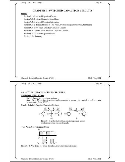
© P.E. Allen, 2001
Analog CMOS Circuit Deisgn
Page 9.1-2
EQUIVALENT RESISTANCE OF A SWITCHED CAPACITOR CIRCUIT Assume that v1(t) and v2(t) are changing slowly with respect to the clock period. The average current is, T T/2 i1(t) i2 (t) 1 1 1 2 ⌠i (t)dt = ⌠i (t)dt ⌡ i1(average) = T ⌡ 1 T 1
0 0 0
C
v2 (t)
However, vC(T/2) = v1(T/2) and vC(0) = v2(0). Therefore, C [v1(T/2)-v2(0)] C [V1-V2] ≈ i1(average) = T T For the continuous time circuit: i1(t) i2 (t) R V -V T ⇒ i1(average) = 1R 2 ∴ R ≈ C v (t) v (t)
T/2
Therefore, i1(average) can be written as, C2 [vC2(T/2)-vC2(0)] C1 [vC1(T)-vC1(T/2)] + i1(average) = T T The sequence of switches cause,vC2(0) = V2, vC2(T/2) = V1, vC1(T/2) = 0, and vC1(T) = V1 - V2. Applying these results gives C2[V1-V2] C1[V1-V2- 0] (C1+C2)(V1-V2) + = i1(average) = T T T T Equating the average current to the continuous time circuit gives: R =C +C 1 2
开关电源输入输出电容的选择

1.2
Selecting Input Ceramic Capacitors
Load current, duty cycle, and switching frequency are several factors which determine the magnitude of the input ripple voltage. The input ripple voltage amplitude is directly proportional to the output load current. The maximum input ripple amplitude occurs at maximum output load. Also, the amplitude of the voltage ripple varies with the duty cycle of the converter. For a single phase buck regulator, the duty cycle is approximately the ratio of output to input dc voltage. A single phase buck regulator reaches its maximum ripple at 50% duty cycle. Figure 1 shows the ac rms, dc, and total rms input current vs duty cycle for a single phase buck regulator. The solid curve shows the ac rms ripple amplitude. It reaches a maximum at 50% duty cycle. The chart shows how this magnitude falls off on either side of 50%. The straight solid line shows the average value or dc component as a function of duty cycle. The curved dashed line shows the total rms current, both dc and ac, of the rectangular pulse as duty cycle varies.
THE WORKING PRINCIPLE OF CMOS DEVICES

THE WORKING PRINCIPLE OF CMOS DEVICESCMOS devices are widely used in integrated circuits. Their working principle is based on the working principle of metal-oxide semiconductor field-effect transistors (MOSFETs). CMOS devices consist of a pair of complementary MOSFETs, including N-type MOSFETs and P-type MOSFETs, which control the conduction state of the two MOSFETs to achieve current control and signal amplification.The working principle of CMOS devices can be divided into three stages: the on stage, the off stage, and the switching stage.In the conduction stage, when the input signal is high, the N-type MOSFET is on and the P-type MOSFET is off. The current flows from the power supply through the N-type MOSFET to the output terminal, forming a high-level output. When the input signal is low, the N-type MOSFET is off and the P-type MOSFET is on. The current flows from the output terminal through the P-type MOSFET to the power supply, forming a low-level output. By controlling the high and low levels of the input signal, the output signal can be controlled.In the off-stage, when the input signal is high, the N-type MOSFET is turned off and the P-type MOSFET is turned on, and the current flows from the output terminal to the power supply, forming a low-level output. When the input signal is low, the N-type MOSFET is turned on and the P-type MOSFET is turned off, and the current flows from the power supply to the output terminal, forming a high-level output. Due to the complementary structure of CMOS devices, low-level and high-level outputs can be achieved.In the switching stage, when the input signal switches from low level to high level, the N-type MOSFET switches from off state to on state, and the P-type MOSFET switches from on state to off state. This switching process requires a certain amount of time, known as the rise time. Similarly, when the input signal switches from high level to low level, the N-type MOSFET and P-type MOSFET also need to switch states, which also requires a certain amount of time, known as the fall time. The speed of switching affects the performance of CMOS devices.The working principle of CMOS devices is based on the working principle of MOSFETs. MOSFETs are a three-layer structure transistor consisting of a source, a drain, and a gate. When a positive voltage is applied to the gate, an electric field is formed, changing the charge density inthe channel and controlling the current between the source and drain. In N-type MOSFETs, when a positive voltage is applied to the gate, the electron concentration in the channel increases, forming a conductive channel, and the current flows from the source to the drain. In P-type MOSFETs, when a negative voltage is applied to the gate, the hole concentration in the channel increases, forming a conductive channel, and the current flows from the drain to the source. CMOS devices control the current by controlling the gate voltage.CMOS devices have many advantages, such as low power consumption, low noise, and strong anti-interference ability. Due to the complementary structure of CMOS devices, the output level can be restored to the power supply level, improving the reliability and stability of the signal. In addition, the manufacturing process of CMOS devices is mature and the production cost is relatively low, making it suitable for the manufacture of large-scale integrated circuits.The working principle of CMOS devices is based on the working principle of MOSFETs, which controls the conduction state of N-type MOSFETs and P-type MOSFETs to achieve current control and signal amplification. CMOS devices have many advantages and are widely used in modern integrated circuits.。
DE250系列高压分离连接器产品介绍说明书

DE250 - 24 kV ApplicationsRelated products• DRC250 Receptacle Cap • DPD250 Dead End Plug • DPS250 Standoff Plug • DPE250 Earthing Plug •DJ250 JunctionsInstallation•No special tools, heating, taping, or potting are required•Connector may be energized immediately after installation on its mating part •Mates with bushings, plugs, and junction devices designed for interface A and complying with the listed standardsApplication•For connection of polymeric cable to transformers, switchgear, motors and other equipment with a premoulded separable connector • For indoor and outdoor installations •Type A interface as described by CENELEC EN 50180 and EN 50181• System voltage up to 24 kV•Continuous current 250 A (300 A overload for 8 hours)•Cable particulars:• Polymeric cable (XLPE, EPR, etc.)• Copper or aluminum conductors •Semiconducting or metallic screens•Conductor size 16-120 mm 2Features•Provides a fully screened and fullysubmersible separable connection when mated with the proper bushing or plug •Built-in capacitive test point to determine the circuit status or install a fault indicator • No minimum phase clearance requirements •Mounting can be vertical, horizontal, or any angle in between •100% factory tested • AC withstand•Partial dischargeStandards•Meets the requirements of Cenelec HD629.1and IEC 60502-4250 A 24 kV class deadbreak elbow connector - interface AQuality assurance•Our manufacturing facility is registered to ISO 9001 by third party audit• Required Production Tests •Periodic X-Ray AnalysisPackaging•Supplied in a kit with parts listed below, approximate weight 1 kgKit contents:• Elbow Housing • Conductor Contact • Pin Contact • Bail Assembly •Hex KeyThe kit also includes lubricant and installation instructions.1. Pin ContactTin-plated copper pin screws into the conductor connector with the supplied hex key.2. Internal ScreenMoulded EPDM conducting rubber screen controls electrical stress.3. InsulationMoulded EPDM insulating rubber is formulated and mixed in-house to ensure high quality.4. Pulling EyeEncapsulated stainless steel pulling eye with a detent to posi-tion the bail.5. Capacitive Test PointCapacitive test point provides means to check circuit status. A moulded EPDM conducting rubber cap provides a water-tight seal.6. Stress ReliefThe configuration of the outer screen and insulation provides cable stress relief.7. Cable EntranceThe sized opening provides an interference fit to maintain a watertight seal.8. External ScreenMoulded EPDM conducting rubber mates with the cable screen to maintain screen continuity and ensure that the assembly is at earth potential.9. Earthing EyeMoulded into the external screen for connection of an earthing wire.10. Conductor ContactInertia welded bimetallic compression connector accepts copper or aluminum conductors.11. Stainless Steel Bail (Figure 2 or 3)Secures the connector to its mating bushing or accessory.Figure 1. 250 A, 24 kV Class DE250 deadbreak elbow connector.①⑧⑨⑩⑦⑤②③④⑥Features and detailed descriptionT able 1. Electrical Ratings Maximum System Voltage (U m )24 kV Impulse125 kV AC Withstand (5 min.)54 kV Continuous Current 250 A Overload (8 hrs Max.)300 A Short Circuit Withstand, 1 sec. (rms sym.)12.5 kA2Catalog Data CA650036ENEffective January 2016250 A deadbreak elbow connector - interface A/cooperpowerseries3Catalog Data CA650036ENEffective January 2016250 A deadbreak elbow connector - interface A /cooperpowerseriesFigure 3. Optional spring loaded bail.Catalog Data CA650036ENEffective January 2016250 A deadbreak elbow connector - interface AEaton1000 Eaton Boulevard Cleveland, OH 44122United States Eaton’s Cooper Power Systems Division 2300 Badger Drive Waukesha, WI 53188/cooperpowerseries © 2016 EatonAll Rights Reserved Printed in USAPublication No. CA650036ENEaton is a registered trademark.All other trademarks are property of their respective owners.。
虚拟机动态扩缩容的策略与实现

虚拟机动态扩缩容的策略与实现虚拟机是一种通过软件模拟硬件功能的计算机系统,它具有独立的操作系统和应用程序。
随着云计算和虚拟化技术的兴起,虚拟机的使用越来越广泛。
但是,随着业务的发展和需求的变化,虚拟机的资源配置问题也逐渐凸显出来。
虚拟机动态扩缩容成为了一项重要的技术。
一、什么是虚拟机动态扩缩容虚拟机动态扩缩容是指根据负载的变化,自动调整虚拟机的资源配置。
当负载较高时,可以增加虚拟机的资源,提高性能和稳定性;当负载较低时,可以减少虚拟机的资源,节约成本和资源。
二、虚拟机动态扩缩容的策略虚拟机动态扩缩容的策略有多种,下面介绍几种常见的策略。
1. 基于阈值的策略基于阈值的策略是最常见的一种,通过设定负载的阈值,当负载超过或低于这个阈值时,自动扩展或缩容虚拟机的资源。
例如,当CPU 使用率超过80%时,自动增加虚拟机的CPU核心数;当CPU使用率低于20%时,自动减少虚拟机的CPU核心数。
2. 基于预测的策略基于预测的策略是根据过去的负载数据和趋势,预测未来的负载情况,从而调整虚拟机的资源配置。
例如,根据过去一周的负载数据,预测未来1小时的负载情况,然后相应地扩容或缩容虚拟机。
3. 基于机器学习的策略基于机器学习的策略是通过分析历史数据,使用机器学习算法来预测未来的负载情况,并根据预测结果调整虚拟机的资源配置。
这种策略可以根据实时的负载情况,不断更新和优化模型,提高预测的准确性。
三、虚拟机动态扩缩容的实现虚拟机动态扩缩容的实现依赖于云平台和虚拟化管理软件的支持。
一般来说,实现虚拟机动态扩缩容需要以下几个步骤:1. 监控负载情况首先,需要监控虚拟机的各种资源使用情况,如CPU、内存、磁盘和网络等。
可以使用监控工具或云平台提供的监控功能,实时获取虚拟机的负载情况。
2. 判断负载状态根据监控数据,判断当前负载的状态,判断是否需要进行扩容或缩容。
可以根据阈值、预测模型或机器学习模型来进行判断。
3. 扩容或缩容虚拟机如果判断需要进行扩容或缩容,就通过云平台或虚拟化管理软件的API,调用相应的命令或接口进行虚拟机的扩容或缩容操作。
有限理性双寡头动态序贯竞争的建模与仿真

文 献 标 识 码 : A
ห้องสมุดไป่ตู้
有 限理 性 双 寡 头 动 态 序 竞 的 建 模 与 仿 真 贯 争
胡 荣 ,夏 洪 山
( 京航空航天大学 民航学院 , 苏 南京 南 江 20 1) 106
摘 要 : 用 非 线 性 动 力 系统 的 分 支 理 论 研 究 了有 限理 性 双 寡 头 Sakleg 量 竞 争 模 型 , 论 了 该 模 型 均 衡 点 的 利 t ebr 产 c 讨
i s— f r t m o e d a t g a a e l a r p o t u d r s m e t p s o yse v r a v n a e c n m k e de r f n e o i y e f s t m l c u t fu t a i on. n a d to c a s I d ii n, h o
c():c t , 中 : 为 常数 , t i () 其 q c 口>c; t 为 产 q( ) 量 , 用 逆 向求 解 法对 模 型进 行 分 析 。 利 在博 弈 时期 t的第 二 阶 段 博 弈 中 , 定 领 先 给
者 企业 1的 产 量 q ( ) 情况 下 , 随者 企 业 2选 。f 的 跟 择 q () 大 化 自己的利 润 , 时企 业 2的 利润 可 t最 此
c a s c nr l h o o t0
更 接 近于 完 全垄 断 的 1 市 场结 构 , 特 点 是 少数 种 其
1 引 言
寡 头 垄 断是 同 时包 含 垄 断 因素 和 竞 争 因 素 而
几 家企 业 占据 了整 个 行 业 中较 高 的市 场 份 额 。在
寡 头垄 断 市 场 中 , 头 企业 的市场 行 为 会 影 响 到竞 寡
Reinforcement learning for dynamic channel allocation in cellular telephone systems
Satinder Singh
Lab. for Info. and Decision Sciences MIT Cambridge, MA 02139 bertsekas@
Dimitri Bertsekas
Abstract
In cellular telephone systems, an important problem is to dynamically allocate the communication resource (channels) so as to maximize service in a stochastic caller environment. This problem is naturally formulated as a dynamic programming problem and we use a reinforcement learning (RL) method to nd dynamic channel allocation policies that are better than previous heuristic solutions. The policies obtained perform well for a broad variety of call trafc patterns. We present results on a large cellular system with approximately 4949 states. In cellular communication systems, an important problem is to allocate the communication resource (bandwidth) so as to maximize the service provided to a set of mobile callers whose demand for service changes stochastically. A given geographical area is divided into mutually disjoint cells, and each cell serves the calls that are within its boundaries (see Figure 1a). The total system bandwidth is divided into channels, with each channel centered around a frequency. Each channel can be used simultaneously at di erent cells, provided these cells are su ciently separated spatially, so that there is no interference between them. The minimum separation distance between simultaneous reuse of the same channel is called the channel reuse constraint . When a call requests service in a given cell either a free channel (one that does not violate the channel reuse constraint) may be assigned to the call, or else the call is blocked from the system; this will happen if no free channel can be found. Also, when a mobile caller crosses from one cell to another, the call is \handed o " to the cell of entry; that is, a new free channel is provided to the call at the new cell. If no such channel is available, the call must be dropped/disconnected from the system.
全国计算机四级考试选择题及答案

全国计算机四级考试选择题及答案全国计算机四级考试选择题及答案全国计算机等级考试采用全国统一命题,统一考试的形式。
今天,店铺特意为大家推荐全国计算机四级考试选择题及答案,希望大家喜欢!选择题(1) 8位二进制原码表示整数的范围是____。
A) 0~+128 B) -128~+128 C) 0~+127 D)-127~+127(2) 在计算机运行时,建立各寄存器之间的“数据通路”并完成取指令和执行指令全过程的部件是____。
A) 时序产生器 B) 程序计数器 C) 操作控制器 D) 指令寄存器(3) 在数据传送过程中,为发现误码甚至纠正误码,通常在源数据数据上附加“校验码”。
其中功能较强的是____。
A)奇偶校验码 B)循环冗余码 C)交叉校验码 D) 横向校验码(4) 设有下三角距阵A[0..10,0..10],按行优先顺序存放其非零元素,则元素A[5,5]的存放地址为____。
A) 110 B) 120 C) 130 D) 140(5) 若一棵二叉树中,度为2的节点数为9,则该二叉树的叶结点数为____。
A) 10 B) 11 C) 12 D) 不确定(6) 设根结点的层次为0,则高度为k的二叉树的最大结点数为____。
A)2k-1 B) 2k C) 2k+1-1 D) 2k+1(7) 设待排序关键码序列为 (25,18,9,33,67,82,53,95,12,70),要按关键码值递增的顺序排序,采取以第一个关键码为分界元素的快速排序法,第一趟排序完成后关键码为33被放到了第几个位置?____。
A) 3 B) 5 C) 7 D) 9(8) 如下所示是一个带权连通无向图,其最小生成树各边权的总和为____。
A) 24 B) 25 C) 26 D) 27(9) 下列命题中为简单命题的是____。
A)张葆丽和张葆华是亲姐妹 B) 张明和张红都是大学生C) 张晖或张旺是河北省人 D) 王际广不是工人(10) 设p:天下大雨,q:我骑自行车上班。
专业英语讲课ppt

Farad abbreviated parallel magnitude Voltage fabricate conjunction maintain peri vt. n. vt. adj. v.
法拉(电容单位) 缩写,简化,简写成,缩写成 平行的,并联的 大小,数量,巨大,广大,量级 电压,伏特数 制作,构成 联合,关联 维持,继续 外围的 n.外围设备 矫正,调整
Capacitors can be fabricated onto integrated circuit(IC) chips. They are commonly used in conjunction with transistors in Dynamic Random Access Memory(DRAM).
utility electrical energy electric field Integrated Circuit(IC) Dynamic Random Access Memory(DRAM) Alternating Current(AC) Direct Current(DC)
n.效用,有用 电能 电场 集成电路 动态随机存取存储器 交流 直流
The capacitors help maintain the contents of memory.
Large capacitors are used in the power supplies of electronic equipment of all types, including computers and their peripherals. In these systems, the capacitors smooth out the rectified utility AC, providing pure, battery-like DC.
微带线无源互调的传输矩阵理论方法

第 21 卷 第 7 期2023 年 7 月太赫兹科学与电子信息学报Journal of Terahertz Science and Electronic Information TechnologyVol.21,No.7Jul.,2023微带线无源互调的传输矩阵理论方法周昊楠a,b,赵小龙*a,b,彭玉彬a,b,曾鸣奇a,b,曹智a,b,张可越a,b,贺永宁*a,b(西安交通大学 a.电子与信息学部微电子学院;b.西安市微纳电子与系统集成重点实验室,陕西西安710049)摘要:均匀微带线是微带电路的基本结构,建立微带线PIM解析模型具有重要意义。
本文基于受控源等效,在微带线的集总电路等效模型中,将微带线中的分布式寄生非线性PIM源建模为二次受控电流源或电压源,从而得到微带线PIM电压和电流关系的传输矩阵表达式,建立了寄生非线性机制的微带线PIM解析计算模型;并通过对比不同长度的镀镍微带线与不同浓度掺磷工艺镀镍微带线的传输互调与反射互调规律,验证本文提出的PIM传输矩阵方法的合理性。
通过该模型提取了镍镀层在0.71 GHz时的三阶相对磁导率非线性系数为1×10⁻¹⁰ m2/A2。
本文方法为进一步建立其他复杂结构微带电路PIM模型提供了新思路。
关键词:无源互调;微带线;寄生非线性;相对磁导率非线性;覆铜板中图分类号:TN015文献标志码:A doi:10.11805/TKYDA2022194Transfer matrix theory for Passive Intermodulation of microstrip linesZHOU Haonan a,b,ZHAO Xiaolong*a,b,PENG Yubin a,b,ZENG Mingqi a,b,CAO Zhi a,b,ZHANG Keyue a,b,HE Yongning*a,b(a.School of Microelectronics,Faculty of Electronic and Information Engineering;b.The Key Laboratory of Micro-Nano Electronics andSystem Integration of Xi'an City,Xi'an Jiaotong University,Xi'an Shaanxi 710049,China)AbstractAbstract::The uniform microstrip line is the basic structure of the microstrip circuit, and it is of great significance to establish the Passive Intermodulation(PIM) analytical model of the microstrip line.Based on the controlled source equivalence, in the lumped circuit equivalent model of the microstrip line,the distributed parasitic nonlinear PIM source in the microstrip line is modeled as a second controlledcurrent source or voltage source, to obtain the matrix expression of the relationship between the voltageand current in the stripline PIM. The analytical calculation model of the uniform microstrip line PIM withthe parasitic nonlinear mechanism is finally established. The experimental verification is carried out bycomparing the transmission intermodulation and reflection intermodulation laws of nickel-platedmicrostrip lines with different lengths and nickel-plated microstrip lines with different concentrations ofphosphorus doping. The third-order relative permeability nonlinear coefficient of nickel coatings isextracted to be 1×10⁻¹⁰ m²/A² at 0.71 GHz. The proposed method based on controlled source equivalenceprovides a new idea for further establishing PIM models of other microstrip circuits.KeywordsKeywords::Passive Intermodulation;microstrip lines;parasitic nonlinearity;nonlinear relative permeability;copper-clad laminate无源互调(PIM)是指2路及以上载波信号馈入微波射频无源器件中时,由于器件或连接等非线性导致载波信号的线性组合产物落入接收机的接收通带内,对接收机形成干扰,使其灵敏度降低的现象。
数字集成电路--电路、系统与设计(第二版)课后练习题 第五章 CMOS反相器
C H A P T E R5T H E C M O S I N V E R T E R Quantification of integrity,performance,and energy metrics of an inverterOptimization of an inverter design5.1Exercises and Design Problems5.2The Static CMOS Inverter—An IntuitivePerspective5.3Evaluating the Robustness of the CMOSInverter:The Static Behavior5.3.1Switching Threshold5.3.2Noise Margins5.3.3Robustness Revisited5.4Performance of CMOS Inverter:The DynamicBehavior5.4.1Computing the Capacitances5.4.2Propagation Delay:First-OrderAnalysis5.4.3Propagation Delay from a DesignPerspective5.5Power,Energy,and Energy-Delay5.5.1Dynamic Power Consumption5.5.2Static Consumption5.5.3Putting It All Together5.5.4Analyzing Power Consumption UsingSPICE5.6Perspective:Technology Scaling and itsImpact on the Inverter Metrics180Section 5.1Exercises and Design Problems 1815.1Exercises and Design Problems1.[M,SPICE,3.3.2]The layout of a static CMOS inverter is given in Figure 5.1.(λ=0.125µm).a.Determine the sizes of the NMOS and PMOS transistors.b.Plot the VTC (using HSPICE)and derive its parameters (V OH ,V OL ,V M ,V IH ,and V IL ).c.Is the VTC affected when the output of the gates is connected to the inputs of 4similargates?.d.Resize the inverter to achieve a switching threshold of approximately 0.75V .Do not lay-out the new inverter,use HSPICE for your simulations.How are the noise margins affected by this modification?2.Figure 5.2shows a piecewise linear approximation for the VTC.The transition region isapproximated by a straight line with a slope equal to the inverter gain at V M .The intersectionof this line with the V OH and the V OL lines defines V IH and V IL .a.The noise margins of a CMOS inverter are highly dependent on the sizing ratio,r =k p /k n ,of the NMOS and PMOS e HSPICE with V Tn =|V Tp |to determine the valueof r that results in equal noise margins?Give a qualitative explanation.b.Section 5.3.2of the text uses this piecewise linear approximation to derive simplifiedexpressions for NM H and NM L in terms of the inverter gain.The derivation of the gain isbased on the assumption that both the NMOS and the PMOS devices are velocity saturatedat V M .For what range of r is this assumption valid?What is the resulting range of V M ?c.Derive expressions for the inverter gain at V M for the cases when the sizing ratio is justabove and just below the limits of the range where both devices are velocity saturated.What are the operating regions of the NMOS and the PMOS for each case?Consider theeffect of channel-length modulation by using the following expression for the small-signalresistance in the saturation region:r o,sat =1/(λI D ).Figure 5.1CMOS inverter layout.InOutGND V DD =2.5V.Poly Metal1NMOSPMOSPolyMetal12λ182THE CMOS INVERTER Chapter 53.[M,SPICE,3.3.2]Figure 5.3shows an NMOS inverter with resistive load.a.Qualitatively discuss why this circuit behaves as an inverter.b.Find V OH and V OL calculate V IH and V IL .c.Find NM L and NM H ,and plot the VTC using HSPICE.d.Compute the average power dissipation for:(i)V in =0V and (ii)V in =2.5Ve HSPICE to sketch the VTCs for R L =37k,75k,and 150k on a single graph.ment on the relationship between the critical VTC voltages (i.e.,V OL ,V OH ,V IL ,V IH )and the load resistance,R L .g.Do high or low impedance loads seem to produce more ideal inverter characteristics?4.[E,None,3.3.3]For the inverter of Figure 5.3and an output load of 3pF:a.Calculate t plh ,t phl ,and t p .b.Are the rising and falling delays equal?Why or why not?pute the static and dynamic power dissipation assuming the gate is clocked as fast as possible.5.The next figure shows two implementations of MOS inverters.The first inverter uses onlyNMOS transistors.V OH V OL inV outFigure 5.2A different approach to derive V IL and V IH .V outV in M 1W/L =1.5/0.5+2.5VFigure 5.3Resistive-load inverterR L =75k ΩSection 5.1Exercises and Design Problems183a.Calculate V OH ,V OL ,V M for each case.e HSPICE to obtain the two VTCs.You must assume certain values for the source/drain areas and perimeters since there is no layout.For our scalable CMOS process,λ =0.125μm,and the source/drain extensions are 5λfor the PMOS;for the NMOS the source/drain contact regions are 5λx5λ.c.Find V IH ,V IL ,NM L and NM H for each inverter and comment on the results.How can you increase the noise margins and reduce the undefined region?ment on the differences in the VTCs,robustness and regeneration of each inverter.6.Consider the following NMOS inverter.Assume that the bulk terminals of all NMOS deviceare connected to GND.Assume that the input IN has a 0V to 2.5V swing.a.Set up the equation(s)to compute the voltage on node x .Assume γ=0.5.b.What are the modes of operation of device M2?Assume γ=0.c.What is the value on the output node OUT for the case when IN =0V?Assume γ=0.d.Assuming γ=0,derive an expression for the switching threshold (V M )of the inverter.Recall that the switching threshold is the point where V IN =V OUT .Assume that the devicesizes for M1,M2and M3are (W/L)1,(W/L)2,and (W/L)3respectively.What are the limitson the switching threshold?For this,consider two cases:i)(W/L)1>>(W/L)2V DD =2.5V V IN V OUTV DD =2.5V V IN V OUT M 2M 1M 4M 3W/L=0.375/0.25W/L=0.75/0.25W/L=0.375/0.25W/L=0.75/0.25Figure 5.4Inverter ImplementationsV DD =2.5V OUTM1IN M2M3V DD =2.5Vx184THE CMOS INVERTER Chapter 5ii)(W/L)2>>(W/L)17.Consider the circuit in Figure 5.5.Device M1is a standard NMOS device.Device M2has allthe same properties as M1,except that its device threshold voltage is negative and has a valueof -0.4V.Assume that all the current equations and inequality equations (to determine themode of operation)for the depletion device M2are the same as a regular NMOS.Assume thatthe input IN has a 0V to 2.5V swing.a.Device M2has its gate terminal connected to its source terminal.If V IN =0V ,what is the output voltage?In steady state,what is the mode of operation of device M2for this input?pute the output voltage for V IN =2.5V .You may assume that V OUT is small to simplify your calculation.In steady state,what is the mode of operation of device M2for this input?c.Assuming Pr (IN =0)=0.3,what is the static power dissipation of this circuit?8.[M,None,3.3.3]An NMOS transistor is used to charge a large capacitor,as shown in Figure5.6.a.Determine the t pLH of this circuit,assuming an ideal step from 0to 2.5V at the input node.b.Assume that a resistor R S of 5k Ωis used to discharge the capacitance to ground.Deter-mine t pHL .c.Determine how much energy is taken from the supply during the charging of the capacitor.How much of this is dissipated in M1.How much is dissipated in the pull-down resistanceduring discharge?How does this change when R S is reduced to 1k Ω.d.The NMOS transistor is replaced by a PMOS device,sized so that k p is equal to the k n ofthe original NMOS.Will the resulting structure be faster?Explain why or why not.9.The circuit in Figure 5.7is known as the source follower configuration.It achieves a DC levelshift between the input and the output.The value of this shift is determined by the current I 0.Assume x d =0,γ=0.4,2|φf |=0.6V ,V T 0=0.43V ,k n ’=115μA/V 2and λ=0.V DD =2.5VOUTM1(4μm/1μm)IN M2(2μm/1μm),V Tn =-0.4VFigure 5.5A depletion load NMOSinverterV DD =2.5VOutFigure 5.6Circuit diagram with annotated W/L ratios=5pFSection 5.1Exercises and Design Problems 185a.Suppose we want the nominal level shift between V i and V o to be 0.6V in the circuit in Figure 5.7(a).Neglecting the backgate effect,calculate the width of M2to provide this level shift (Hint:first relate V i to V o in terms of I o ).b.Now assume that an ideal current source replaces M2(Figure 5.7(b)).The NMOS transis-tor M1experiences a shift in V T due to the backgate effect.Find V T as a function of V o for V o ranging from 0to 2.5V with 0.5V intervals.Plot V T vs.V oc.Plot V o vs.V i as V o varies from 0to 2.5V with 0.5V intervals.Plot two curves:one neglecting the body effect and one accounting for it.How does the body effect influence the operation of the level converter?d.At V o (with body effect)=2.5V,find V o (ideal)and thus determine the maximum error introduced by the body effect.10.For this problem assume:V DD =2.5V ,W P /L =1.25/0.25,W N /L =0.375/0.25,L =L eff =0.25μm (i.e.x d =0μm),C L =C inv-gate ,k n ’=115μA/V 2,k p ’=-30μA/V 2,V tn0=|V tp0|=0.4V,λ =0V -1, γ=0.4,2|φf |=0.6V ,and t ox =e the HSPICE model parameters for parasitic capacitance given below (i.e.C gd0,C j ,C jsw ),and assume that V SB =0V for all problems except part (e).Figure 5.7NMOS source follower configuration V DD =2.5V V iV oV DD =2.5VV i V oV bias =(a)(b)I o1um/0.25um M1186THE CMOS INVERTER Chapter 5##Parasitic Capacitance Parameters (F/m)##NMOS:CGDO=3.11x10-10,CGSO=3.11x10-10,CJ=2.02x10-3,CJSW=2.75x10-10PMOS:CGDO=2.68x10-10,CGSO=2.68x10-10,CJ=1.93x10-3,CJSW=2.23x10-10a.What is the V m for this inverter?b.What is the effective load capacitance C Leff of this inverter?(include parasitic capacitance,refer to the text for K eq and m .)Hint:You must assume certain values for the source/drain areas and perimeters since there is no layout.For our scalable CMOS process,λ =0.125μm,and the source/drain extensions are 5λfor the PMOS;for the NMOS the source/drain contact regions are 5λx5λ.c.Calculate t PHL ,t PLH assuming the result of (b)is ‘C Leff =6.5fF’.(Assume an ideal step input,i.e.t rise =t fall =0.Do this part by computing the average current used to charge/dis-charge C Leff .)d.Find (W p /W n )such that t PHL =t PLH .e.Suppose we increase the width of the transistors to reduce the t PHL ,t PLH .Do we get a pro-portional decrease in the delay times?Justify your answer.f.Suppose V SB =1V,what is the value of V tn ,V tp ,V m ?How does this qualitatively affect C Leff ?ing Hspice answer the following questions.a.Simulate the circuit in Problem 10and measure t P and the average power for input V in :pulse(0V DD 5n 0.1n 0.1n 9n 20n),as V DD varies from 1V -2.5V with a 0.25V interval.[t P =(t PHL +t PLH )/2].Using this data,plot ‘t P vs.V DD ’,and ‘Power vs.V DD ’.Specify AS,AD,PS,PD in your spice deck,and manually add C L =6.5fF.Set V SB =0Vfor this problem.b.For Vdd equal to 2.5V determine the maximum fan-out of identical inverters this gate candrive before its delay becomes larger than 2ns.c.Simulate the same circuit for a set of ‘pulse’inputs with rise and fall times of t in_rise,fall =1ns,2ns,5ns,10ns,20ns.For each input,measure (1)the rise and fall times t out_rise andV DD =2.5VV IN V OUTC L =C inv-gateL =L P =L N =0.25μmV SB-+(W p /W n =1.25/0.375)Figure 5.8CMOS inverter with capacitiveSection 5.1Exercises and Design Problems 187t out_fall of the inverter output,(2)the total energy lost E total ,and (3)the energy lost due to short circuit current E short .Using this data,prepare a plot of (1)(t out_rise +t out_fall )/2vs.t in_rise,fall ,(2)E total vs.t in_rise,fall ,(3)E short vs.t in_rise,fall and (4)E short /E total vs.t in_rise,fall.d.Provide simple explanations for:(i)Why the slope for (1)is less than 1?(ii)Why E short increases with t in_rise,fall ?(iii)Why E total increases with t in_rise,fall ?12.Consider the low swing driver of Figure 5.9:a.What is the voltage swing on the output node (V out )?Assume γ=0.b.Estimate (i)the energy drawn from the supply and (ii)energy dissipated for a 0V to 2.5V transition at the input.Assume that the rise and fall times at the input are 0.Repeat the analysis for a 2.5V to 0V transition at the input.pute t pLH (i.e.the time to transition from V OL to (V OH +V OL )/2).Assume the input rise time to be 0.V OL is the output voltage with the input at 0V and V OH is the output volt-age with the input at 2.5V .pute V OH taking into account body effect.Assume γ =0.5V 1/2for both NMOS and PMOS.13.Consider the following low swing driver consisting of NMOS devices M1and M2.Assumean NWELL implementation.Assume that the inputs IN and IN have a 0V to 2.5V swing andthat V IN =0V when V IN =2.5V and vice-versa.Also assume that there is no skew between INand IN (i.e.,the inverter delay to derive IN from IN is zero).a.What voltage is the bulk terminal of M2connected to?V in V out V DD =2.5V W L 3μm 0.25μm =p 2.5V0V C L =100fFW L 1.5μm 0.25μm=n Figure 5.9Low Swing DriverV LOW =0.5VOutM1ININ M225μm/0.25μm 25μm/0.25μmC L =1pFFigure 5.10Low Swing Driver188THE CMOS INVERTER Chapter 5b.What is the voltage swing on the output node as the inputs swing from 0V to 2.5V .Showthe low value and the high value.c.Assume that the inputs IN and IN have zero rise and fall times.Assume a zero skewbetween IN and IN.Determine the low to high propagation delay for charging the outputnode measured from the the 50%point of the input to the 50%point of the output.Assumethat the total load capacitance is 1pF,including the transistor parasitics.d.Assume that,instead of the 1pF load,the low swing driver drives a non-linear capacitor,whose capacitance vs.voltage is plotted pute the energy drawn from the lowsupply for charging up the load capacitor.Ignore the parasitic capacitance of the driver cir-cuit itself.14.The inverter below operates with V DD =0.4V and is composed of |V t |=0.5V devices.Thedevices have identical I 0and n.a.Calculate the switching threshold (V M )of this inverter.b.Calculate V IL and V IH of the inverter.15.Sizing a chain of inverters.a.In order to drive a large capacitance (C L =20pF)from a minimum size gate (with inputcapacitance C i =10fF),you decide to introduce a two-staged buffer as shown in Figure5.12.Assume that the propagation delay of a minimum size inverter is 70ps.Also assumeV DD =0.4VV IN V OUTFigure 5.11Inverter in Weak Inversion RegimeSection 5.1Exercises and Design Problems 189that the input capacitance of a gate is proportional to its size.Determine the sizing of thetwo additional buffer stages that will minimize the propagation delay.b.If you could add any number of stages to achieve the minimum delay,how many stages would you insert?What is the propagation delay in this case?c.Describe the advantages and disadvantages of the methods shown in (a)and (b).d.Determine a closed form expression for the power consumption in the circuit.Consider only gate capacitances in your analysis.What is the power consumption for a supply volt-age of 2.5V and an activity factor of 1?16.[M,None,3.3.5]Consider scaling a CMOS technology by S >1.In order to maintain compat-ibility with existing system components,you decide to use constant voltage scaling.a.In traditional constant voltage scaling,transistor widths scale inversely with S,W ∝1/S.To avoid the power increases associated with constant voltage scaling,however,youdecide to change the scaling factor for W .What should this new scaling factor be to main-tain approximately constant power.Assume long-channel devices (i.e.,neglect velocitysaturation).b.How does delay scale under this new methodology?c.Assuming short-channel devices (i.e.,velocity saturation),how would transistor widthshave to scale to maintain the constant power requirement?1InAdded Buffer StageOUTC L =20pF C i =10fF‘1’is the minimum size inverter.??Figure 5.12Buffer insertion for driving large loads.190THE CMOS INVERTER Chapter5DESIGN PROBLEMUsing the0.25μm CMOS introduced in Chapter2,design a static CMOSinverter that meets the following requirements:1.Matched pull-up and pull-down times(i.e.,t pHL=t pLH).2.t p=5nsec(±0.1nsec).The load capacitance connected to the output is equal to4pF.Notice that thiscapacitance is substantially larger than the internal capacitances of the gate.Determine the W and L of the transistors.To reduce the parasitics,useminimal lengths(L=0.25μm)for all transistors.Verify and optimize the designusing SPICE after proposing a first design using manual -pute also the energy consumed per transition.If you have a layout editor(suchas MAGIC)available,perform the physical design,extract the real circuitparameters,and compare the simulated results with the ones obtained earlier.。
机械设计名词之实效状态VC及合成状态RC
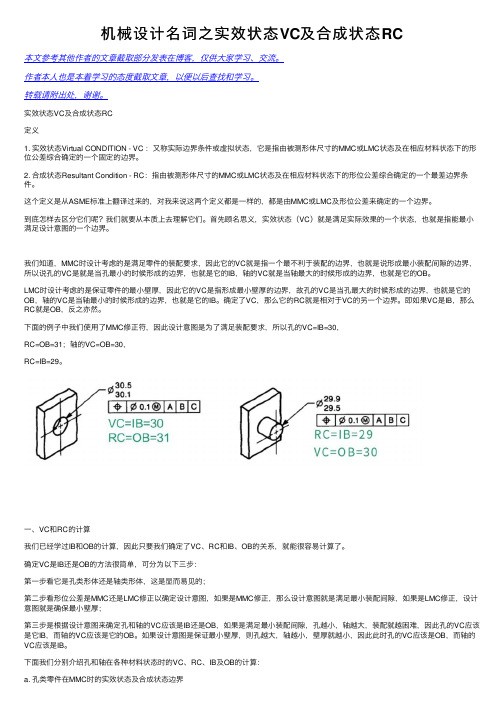
机械设计名词之实效状态VC及合成状态RC本⽂参考其他作者的⽂章截取部分发表在博客,仅供⼤家学习、交流。
作者本⼈也是本着学习的态度截取⽂章,以便以后查找和学习。
转载请附出处,谢谢。
实效状态VC及合成状态RC定义1. 实效状态Virtual CONDITION - VC :⼜称实际边界条件或虚拟状态,它是指由被测形体尺⼨的MMC或LMC状态及在相应材料状态下的形位公差综合确定的⼀个固定的边界。
2. 合成状态Resultant Condition - RC:指由被测形体尺⼨的MMC或LMC状态及在相应材料状态下的形位公差综合确定的⼀个最差边界条件。
这个定义是从ASME标准上翻译过来的,对我来说这两个定义都是⼀样的,都是由MMC或LMC及形位公差来确定的⼀个边界。
到底怎样去区分它们呢?我们就要从本质上去理解它们。
⾸先顾名思义,实效状态(VC)就是满⾜实际效果的⼀个状态,也就是指能最⼩满⾜设计意图的⼀个边界。
我们知道,MMC时设计考虑的是满⾜零件的装配要求,因此它的VC就是指⼀个最不利于装配的边界,也就是说形成最⼩装配间隙的边界,所以说孔的VC是就是当孔最⼩的时候形成的边界,也就是它的IB,轴的VC就是当轴最⼤的时候形成的边界,也就是它的OB。
LMC时设计考虑的是保证零件的最⼩壁厚,因此它的VC是指形成最⼩壁厚的边界,故孔的VC是当孔最⼤的时候形成的边界,也就是它的OB,轴的VC是当轴最⼩的时候形成的边界,也就是它的IB。
确定了VC,那么它的RC就是相对于VC的另⼀个边界。
即如果VC是IB,那么RC就是OB,反之亦然。
下⾯的例⼦中我们使⽤了MMC修正符,因此设计意图是为了满⾜装配要求,所以孔的VC=IB=30,RC=OB=31;轴的VC=OB=30,RC=IB=29。
⼀、VC和RC的计算我们已经学过IB和OB的计算,因此只要我们确定了VC、RC和IB、OB的关系,就能很容易计算了。
确定VC是IB还是OB的⽅法很简单,可分为以下三步:第⼀步看它是孔类形体还是轴类形体,这是显⽽易见的;第⼆步看形位公差是MMC还是LMC修正以确定设计意图,如果是MMC修正,那么设计意图就是满⾜最⼩装配间隙,如果是LMC修正,设计意图就是确保最⼩壁厚;第三步是根据设计意图来确定孔和轴的VC应该是IB还是OB,如果是满⾜最⼩装配间隙,孔越⼩,轴越⼤,装配就越困难,因此孔的VC应该是它IB,⽽轴的VC应该是它的OB。
可扩展验证克服现有验证方法的局限性

可扩展验证克服现有验证方法的局限性随着芯片设计规模和设计复杂度日益增加(包括软件设计和模拟设计在总设计工作中所占的比重日益增加),功能验证的重要性也日益凸显。
所谓设计规模增加,是指一块SoC上所包含的晶体管数量变得惊人的多,这就导致其中包含的门也越来越多。
如今,仅一块SoC上就已经可以包含上千万个门,这无形中增大了电路出错的几率,也使验证工作变得更加复杂。
而所谓设计复杂度增加,则指一块单独的芯片上包含的组件种类增多,不同种类组件的数量也变多。
这里所说的组件包括高性能CPU、多个千兆I/O、嵌入式RAM、系统时钟管理组件、模拟混合信号、嵌入式软件和专用数字信号处理器(DSP)。
随着这些组件的种类和数量增加,对芯片的整体功能和性能而言,各组件之间的接口就变得越发重要。
此外,片上软件和模拟器件也越来越频繁地出现在芯片中,这又进一步提升了系统的复杂度,同时对传统的验证方法提出了挑战。
首先,数字设计工程师们必须面对一些他们并不熟悉的模拟设计方面的问题。
其次,许多硬件设计都要求固件或低级软件就绪而且可以工作后才能验证RTL的功能。
这就要求固件设计师必须在硬件设计中扮演重要角色,仔细协调软、硬件之间的相互关系。
这就是说,我们必须改变设计方法。
用一句老话说,要么做得更好,要么就换种方法来做。
想做得更好就必须研究现有方法所采用的工具及其效率,而换种方法来做则必须改变方法以获得更高的效率。
这两种方式之间不存在谁对谁错,但更有效的方式则是随着时间推移,将二者中的一些元素结合起来,并在恰当的时刻应用到我们的验证方法中去。
要改进现有方法,首先必须研究各种工具本身,以及它们之间的相互关系。
为此,我们需要能够涵盖以下验证域的工具:软仿真、硬仿真、硬件、软件,以及模拟和数字域。
此外,这些工具还必须支持所有标准和新兴的设计语言,包括VHDL、Verilog、PSL、C、SystemC,以及最新的SystemVerilog。
在某种程度上说,这就是我们所说的可扩展验证(Scalable Verification )。
- 1、下载文档前请自行甄别文档内容的完整性,平台不提供额外的编辑、内容补充、找答案等附加服务。
- 2、"仅部分预览"的文档,不可在线预览部分如存在完整性等问题,可反馈申请退款(可完整预览的文档不适用该条件!)。
- 3、如文档侵犯您的权益,请联系客服反馈,我们会尽快为您处理(人工客服工作时间:9:00-18:30)。
Dynamic Capacitated Minimum Spanning TreesRaja Jothi and Balaji RaghavachariDepartment of Computer Science,University of Texas at DallasRichardson,TX75083,USAraja,rbk@Abstract—Given a set of terminals,each associated witha positive number denoting the traffic to be routed to a central terminal(root),the Capacitated Minimum SpanningTree(CMST)problem asks for a minimum spanning tree, spanning all terminals,such that the amount of traffic routedfrom a subtree,linked to the root by an edge,does not exceed the given capacity constraint.The CMST problem is NP-complete and has been extensively studied for the past40years.Current best heuristics,in terms of costand computation time(),are due to Esau and Williams[1],and Jothi and Raghavachari[2].In this paper,we consider the Dynamic Capacitated Min-imum Spanning Tree(DCMST)problem in which a CMST ,spanning nodes and rooted at a central node,with capacity constraint is given as part of the input.Requests, from new nodes,for joining arrive dynamically(online), one at a time.Under this setting,we want to add the new node to the existing CMST without having to recompute the entire CMST,which would take time.To our knowledge, the DCMST problem has not been studied before.For the DCMST problem,we propose three methods(COD,CFOD and BSA)to add the new nodes to the existing CMST.All our heuristics run in linear time.We compare the performance of our heuristics with a CMST algorithm that recomputes the solution every time a new node arrives.Keywords—Capacitated Minimum Spanning Trees,Net-work Design,Dynamic Graph Algorithms.I.I NTRODUCTIONMany network design problems involvefinding min-imum cost spanning trees satisfying certain connectiv-ity constraints.Unfortunately,many such problems are intractable(NP-hard).Due to this reason,the research community has turned its attention onfinding fast and efficient heuristics to solve these computationally“hard”problems.One of the well-studied problems in thefield of telecom-munications is the Capacitated Minimum Spanning Tree (CMST)problem.Given a set of terminals,each associated with a positive number denoting the traffic to be routed to the central terminal(root),the CMST problem asks for a minimum spanning tree,spanning all terminals,such that the amount of traffic routed from a subtree,linked to the root by an edge,does not exceed the given capacity constraint.Each edge connecting two nodes have a cost associated with ually,the cost of a edge is proportional to its length.The CMST problem is NP-hard[3],[4].In the design of telecommunication networks,the CMST problem corresponds to the designing of aminimum cost tree network by installing expensive(fiber-optic)cables along its edges,with a capacity constraint on the cable being used.The cables are assumed to be bought at unit cost per unit length.Since the cable capacityis,every subtree,connected to the root using an edge, can route a traffic of at most to the root.Throughout this paper,the terms terminals,nodes and vertices are used interchangeably.The CMST problem can formally be defined as follows:CMST:Given an undirected vertex-weighted graph ,where is the set of nodes and is the set of edges connecting the nodes,root node,and an integer.The CMST problem asks for a minimum spanning tree with the sum of the vertex weights of every subtree,connected to by an edge,at most.The CMST problem has been extensively studied inComputer Science and Operations Research for the past40years.Several heuristics and exact algorithms have beenproposed(see Section I-B for more details).The most popular and efficient heuristic for the CMST problem is due to Esau and Williams[1].In recent work,Jothi and Raghavachari[2]proposed a new heuristic that performs better than that of Esau and Williams.Both heuristics run in time.There are other heuristics[5],[6], [7]based on Tabu Search and Simulated Annealing,which perform better in terms of the quality of the solution,but their running times are much higher.For other heuristics and exact algorithms on the CMST problem,we refer the reader to[5].For worst-case performance ratios and approximation algorithms on the CMST problem,we refer the reader to[8],[9],[10].A.The DCMST ProblemMany problems in thefield of communication networks are designed as graph problems.Even though,in most cases,the input graphs are static(remain unchanged), there are situations in which graphs are subject to discrete changes,such as addition and deletion of nodes or edges. Networks,represented as graphs,that experience changes in the topology are called dynamic networks.An interesting problem in dealing with dynamically changing networks is to perform the updates swiftly and efficiently without having to shutdown the entire system.In real life situations,it is quite normal for new nodes to join the already available(or functioning)network.While it could be cost efficient to recompute the overall network topology due to the addition of the new node,it is more time consuming to do so.Also,it is desirable that joining of the new nodes causes less inconvenience to the already functioning connected nodes.In this context,we consider the Dynamic Capaci-tated Minimum Spanning Tree(DCMST)problem.In the DCMST problem,a CMST,spanning nodes and rooted at a central node,with capacity constraint is given aspart of the input.Requests,from new nodes which are not in,wishing to join the existing CMST arrive dynamically (online),one at a time.Under this setting,we want to add the new nodes,one at a time as they arrive,to the existing CMST without having to recompute the entire CMST,which would take time.Since every node in the CMST problem is associated a weight,which denotes the amount of traffic that is to be routed to the central node,every new request comes with a weight value associated the node that is to be connected to.To our knowledge,the DCMST problem has not been studied before.In this paper,we propose three methods to add the new node to the existing CMST.All our heuristics run in time.We compare the results of our heuristics with the results obtained from recomputing the solution every time a new node expresses its interest to join the existing CMST.B.Related WorkAlgorithms forfinding a minimum spanning tree(MST) are well known.Amato et al.[11]and Cattaneo et al.[12] studied dynamic minimum spanning tree algorithms for maintaining minimum spanning trees in dynamic graphs. Demetrescu and Italiano[13]presented a fully dynamic algorithm for maintaining all pair shortest paths in dynamic directed graphs with real-valued edge weights.Galil and Italiano[14],[15]presented fully dynamic algorithms for edge connectivity problems.For more details on dynamic graph algorithms,we refer the reader to[11],[16].The remainder of this paper is organized as follows. In Section II,we present our heuristics for the DCMST problem.Section III contains the experimental results of the heuristics.Finally,Section IV contains our concluding remarks and directions for future research.II.H EURISTICS FOR THE DCMST PROBLEMIn this section,we present three heuristics for the DCMST problem.Any heuristic for the DCMST problem will have a worst-case running time of at least.This is due to the reason that for every new node that wishes to join the existing CMST,it takes time to compute the distances between that node and the rest of the nodes in the existing CMST.If the distance vector is given as a part of the input along with the new node,then one can choose to connect the new node to an arbitrary node in the tree(provided the capacity constraint is not violated) or to the central node.This naive approach will make the running time constant,but the cost of the tree will increase uncontrollably.We consider the case when the distance vectors are not given as part of the input.All our heuristics run in linear time.Before we proceed to the heuristics,we define a few terms.Let be the CMST to which a new node is to be connected.Let be the root node of.Let denote the capacity constraint on.Let denote the distance between nodes and.We use the term cluster to refer to the subtrees rooted at the children of.A.The closest-or-direct(COD)heuristicThe new node is connected to the closest node in the CMST,provided that the sum of the vertex weights in the cluster containing plus the vertex weight of is at most,and.Otherwise,is directly connected to.The time to compute the distances between and the nodes in is linear.During the computation of distances between and the nodes in,’s closest node can be found.Once’s closest node is known,it takes constant time to connect to.Thus the overall time complexity of the COD heuristic is linear.B.The closest feasible or direct(CFOD)heuristicThe new node is connected to the closest node in the CMST,provided that the following two conditions are satisfied:1).2)the sum of the vertex weights in the cluster contain-ing plus the vertex weight of is at most.If thefirst condition is not satisfied,is directly connected to.If the second condition is not satisfied,we repeat the above with’s second closest node and so on,until is included in the tree.The CFOD heuristic can be implemented in linear time. The time to compute the distances between and the nodes in is linear.During the computation of dis-tances between and the nodes in,compute the value.If, then is connected to node that contributed to ,otherwise is directly connected to.C.The best savings(BSA)heuristicThe new node is connected to node in the CMST, which provides the greatest savings.This heuristic is in line with Esau and Williams algorithm[1].Let be the cluster containing and be the distance between and its closest node in.Let.During the computation of distances between and the nodes in,compute the savings and for every node .Keep track of the node for which the savingsproduced(either or)is positive and maximum under the condition that the sum of vertex weights in plus the vertex weight of is at most.Connect and if the savings are positive,else connect to directly.The time to compute the distances between and the nodes in is linear.Since the node in to whichis connected is found during the computation of distances between and the nodes in,the running time of BSA heuristic is linear.III.E XPERIMENTAL R ESULTSWe conducted simulations to study the performance of our heuristics against a CMST heuristic(Esau and Williams algorithm[1])which recomputes the solution every time a new node has to be connected to the already existing CMST.Obviously recomputing the CMST will produce better solutions when compared to our heuristics.But since the goal behind dynamic graph algorithms is to perform updates without having to recompute the entire solution, running time is very crucial,apart from not disturbing the operation of the existing nodes considerably.Since there is no proper lower bound with which one can compare dynamic online algorithms,it is of normal practice to compare dynamic online algorithms with offline algorithms which recompute the entire solution.Each input instance contains a CMST of100nodes with capacity constraint,which was computed using the Esau and Williams algorithm[1].The nodes in the CMST were generated using a random distribution of points in a grid.The cost of an edge that connects points and is the Euclidean distance between and.For each instance,50new nodes were generated uniformly at random.Every time a new node is generated,it has to be connected to the CMST.We test our heuristics for both weighted and unweighted versions of the DCMST problem. In the unweighted DCMST version,the weights of all the node is set to1.That is,each node has a traffic of1unit that has to be routed to the root node.In the weighted DCMST version,each node is associated with an arbitrary weight less than or equal to the capacity constraint. For each value,we generated100instances,with each instance starting with a100node CMST and performing addition of50new nodes.For each value,we computed the average cost of the tree after the addition of new node,where.Table I shows the average time to perform the addition of new node to the existing tree. Figures1to8compare the changes in the cost of the tree for all the three heuristics proposed in this paper and the Esau and Williams(EW)algorithm[1].Our experimental results show that CFOD and BSA produce the best results among the three proposed heuristics.In terms of time, CFOD is little faster than BSA.The fastest in terms of time is the COD heuristic,but it does not produce good results.While the worst-case running times of the three proposed heuristics are linear,the worst-case running time of EW algorithm is.IV.C ONCLUSIONIn this paper,we considered the dynamic capacitated minimum spanning tree problem.We presented three heuristics for the DCMST problem and compared their per-formance with the CMST algorithm(Esau and Williams) that recomputes the solution every time a new node arrives. Our experiments show that two of our heuristics(CFOD and BSA)produce the best results.The CFOD heurstic is slightly faster than the BSA heuristic.Our other heuristic (COD)is the fastest among the three heuristics,but the quality of the solutions were not as good as that of CFOD and BSA.The worst-case running times of all our heuristics are linear.We are currently investigating several other heuristics for the DCMST problem.A CKNOWLEDGMENTThis research was supported by the National Science Foundation under grant CCR-9820902.R EFERENCES[1]L.R.Esau and K.C.Williams,“On teleprocessing system design,”IBM Sys.Journal,V ol.5,pp.142-147,1966.[2]R.Jothi and B.Raghavachari,“Design of local access networks,”to appear in Proc.of the15th IASTED Intl.Conf.on Parallel and Distributed Comput.and Systems(PDCS),2003.[3]M.R.Garey and D.S.Johnson,Computers and intractability:Aguide to the theory of NP-completeness,W.H.Freeman,San Fran-cisco,1979.[4] C.H.Papadimitriou,“The complexity of the capacitated tree prob-lem,”Networks,8,pp.217-230,1978.[5] A.Amberg,W.Domschke and S.V o,“Capacitated minimumspanning trees:Algorithms using intelligent search,”Comb.Opt.: Theory and Practice,1,pp.9-39,1996.[6]R.K.Ahuja,J.B.Orlin and D.Sharma,“A composite neighborhoodsearch algorithm for the capacitated minimum spanning tree prob-lem,”Manuscript,2001.[7]Y.M.Sharaiha,M.Gendreau,porte and I.H.Osman,“A tabusearch algorithm for the capacitated shortest spanning tree problem,”Networks,29,pp.161-171,1997.[8]K.Altinkemer and B.Gavish,“Heuristics with constant errorguarantees for the design of tree networks,”Management Science, V ol.34,pp.331-341,1988.[9]R.Jothi and B.Raghavachari,“Topological design of centralizedcommunication networks,”Manuscript,2003.[10]R.Jothi and B.Raghavachari,“Approximation algorithms for thecapacitated minimum spanning tree problem and its variants in network design,”Manuscript,2003.[11]G.Amato,G.Cattaneo and G.F.Italiano,“Experimental analysis ofdynamic minimum spanning tree algorithms,”Proc.8th ACM-SIAM Annual Symp.on Disc.Algorithms(SODA),pp.314–323,1997. [12]G.Cattaneo,P.Faruolo,U.Ferraro Petrillo and G.F.Italiano,“Maintaining dynamic minimum spanning trees:An experimental study,”Proc.4th Workshop on Alg.Engg.and Experiments,2002.[13] C.Demetrescu and G.F.Italiano,“Fully dynamic all pairs shortestpaths with real edge weights,”Proc.42nd IEEE Annual Symp.on Foundations of Computer Science(FOCS),pp.260-267,2001. [14]Z.Galil and G.F.Italiano,“Fully dynamic algorithms for edgeconnectivity problems,”ACM Symposium on Theory of Computing, pp.317-327,1991.[15]Z.Galil and G.F.Italiano,“Fully dynamic algorithms for2-edge-connectivity,”SIAM puting,V ol.21,pp.1047-1069,1992.[16] D.Eppstein,Z.Galil and G.F.Italiano,“Dynamic graph algorithms,”Algorithms and Theory of Computation Handbook,CRC Press, 1999.[17] D.Alberts,G.Cattaneo and G.F.Italiano,“An experimental studyof dynamic graph algorithms,”ACM Journal on Experimental Al-gorithmics,V ol.2,1997.Time (in milliseconds)Unit weight vertices?COD BSA3235.490.185149.880.101095.330.122064.400.06No 0.020.44No 0.000.36No 0.080.34No0.020.24TABLE IA VERAGE RUNNING TIME FOR EACH UPDATE .200025003000350040004500100105110115120125130135140145150C o s t o f t h e t r e eNumber of nodes in the treeOffline EWCOD CFOD BSAFig.1.Average cost of the tree after each node update (unit weight nodes with ).140016001800200022002400260028003000320034003600100105110115120125130135140145150C o s t o f t h e t r e eNumber of nodes in the treeOffline EWCOD CFOD BSAFig.2.Average cost of the tree after each node update (unit weight nodes with .)80010001200140016001800200022002400260028003000100105110115120125130135140145150C o s t o f t h e t r e eNumber of nodes in the treeOffline EWCOD CFOD BSAFig.3.Average cost of the tree after each node update (unit weightnodes with .)600800100012001400160018002000220024002600100105110115120125130135140145150C o s t o f t h e t r e eNumber of nodes in the treeOffline EWCOD CFOD BSAFig.4.Average cost of the tree after each node update (unit weightnodes with .)300035004000450050005500100105110115120125130135140145150C o s t o f t h e t r e eNumber of nodes in the treeOffline EWCOD CFOD BSAFig.5.Average cost of the tree after each node update (arbitrary weightednodes with.)150020002500300035004000100105110115120125130135140145150C o s t o f t h e t r e eNumber of nodes in the treeOffline EWCOD CFOD BSAFig.6.Average cost of the tree after each node update (arbitrary weightednodes with.)120014001600180020002200240026002800300032003400100105110115120125130135140145150C o s t o f t h e t r e eNumber of nodes in the treeOffline EWCOD CFOD BSAFig.7.Average cost of the tree after each node update (arbitrary weightednodes with.)1000120014001600180020002200240026002800100105110115120125130135140145150C o s t o f t h e t r e eNumber of nodes in the treeOffline EWCOD CFOD BSAFig.8.Average cost of the tree after each node update (arbitrary weightednodes with.)。