MPSW14中文资料
MPSW42G;MPSW42RLRA;MPSW42RLRAG;MPSW42;中文规格书,Datasheet资料
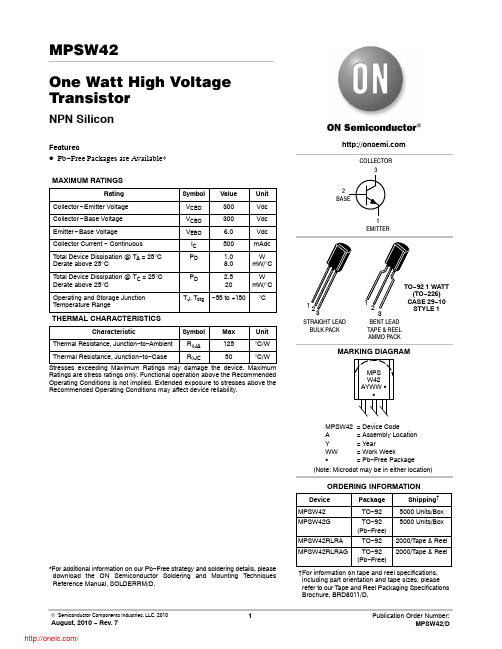
MPSW42One Watt High Voltage TransistorNPN SiliconFeatures•Pb−Free Packages are Available*MAXIMUM RATINGSRating Symbol Value Unit Collector−Emitter Voltage V CEO300Vdc Collector−Base Voltage V CBO300Vdc Emitter−Base Voltage V EBO 6.0Vdc Collector Current − Continuous I C500mAdcTotal Device Dissipation @ T A = 25°C Derate above 25°C P D 1.08.0WmW/°CTotal Device Dissipation @ T C = 25°C Derate above 25°C P D 2.520WmW/°COperating and Storage Junction Temperature Range T J, T stg−55 to +150°CTHERMAL CHARACTERISTICSCharacteristic Symbol Max Unit Thermal Resistance, Junction−to−Ambient R q JA125°C/W Thermal Resistance, Junction−to−Case R q JC50°C/W Stresses exceeding Maximum Ratings may damage the device. Maximum Ratings are stress ratings only. Functional operation above the Recommended Operating Conditions is not implied. Extended exposure to stresses above the Recommended Operating Conditions may affect device reliability.*For additional information on our Pb−Free strategy and soldering details, please download the ON Semiconductor Soldering and Mounting Techniques Reference Manual, SOLDERRM/D.†For information on tape and reel specifications, including part orientation and tape sizes, please refer to our T ape and Reel Packaging Specifications Brochure, BRD8011/D.MPSW42RLRA TO−922000/T ape & Reel MPSW42RLRAG TO−92(Pb−Free)2000/T ape & Reel DevicePackage Shipping†MPSW42TO−925000 Units/Box MPSW42G TO−92(Pb−Free)5000 Units/Box MPSW42= Device CodeA= Assembly LocationY= YearWW= Work WeekG= Pb−Free Package(Note: Microdot may be in either location)ORDERING INFORMATIONCOLLECTOR21EMITTERMARKING DIAGRAMMPSW42AYWW GGBENT LEADTAPE & REELAMMO PACKSTRAIGHT LEADBULK PACK−92 1 WATT(TO−226)−10STYLE 1ELECTRICAL CHARACTERISTICS (T A = 25°C unless otherwise noted)Characteristic Symbol Min Max Unit OFF CHARACTERISTICSCollector−Emitter Breakdown Voltage (Note 1)(I C = 1.0 mAdc, I B = 0)V(BR)CEO300−VdcCollector−Base Breakdown Voltage(I C = 100 m Adc, I E = 0)V(BR)CBO300−VdcEmitter−Base Breakdown Voltage(I E = 100 m Adc, I C = 0)V(BR)EBO 6.0−VdcCollector Cutoff Current(V CB = 200 Vdc, I E = 0)I CBO−0.1m AdcEmitter Cutoff Current(V EB = 6.0 Vdc, I C = 0)I EBO−0.1m Adc ON CHARACTERISTICSDC Current Gain(I C = 1.0 mAdc, V CE = 10 Vdc)(I C = 10 mAdc, V CE = 10 Vdc)(I C = 30 mAdc, V CE = 10 Vdc)h FE254040−−−−Collector−Emitter Saturation Voltage(I C = 20 mAdc, I B = 2.0 mAdc)V CE(sat)−0.5VdcBase−Emitter Saturation Voltage(I C = 20 mAdc, I B= 2.0 mAdc)V BE(sat)−0.9Vdc SMALL−SIGNAL CHARACTERISTICSCurrent−Gain − Bandwidth Product(I C = 10 mAdc, V CE = 20 Vdc, f = 20 MHz)f T50−MHzCollector Capacitance(V CB = 20 Vdc, I E = 0, f = 1.0 MHz)C cb− 3.0pF1.Pulse Test: Pulse Width v 300 m s, Duty Cycle v2.0%.C , C A P A C I T A N C E (p F )Figure 1. DC Current GainV R , REVERSE VOLTAGE (VOLTS)1000Figure 2. CapacitanceI C , COLLECTOR CURRENT (mA)V , V O L T A G E (V O L T S )1.40.01.21.00.80.60.40.2100100.11.0100Figure 3. ”ON” VoltagesI C , COLLECTOR CURRENT (mA)1200.1 1.01010080600h F E , D C C U R R E N T G A I N1002040PACKAGE DIMENSIONSTO −92 (TO −226) 1 WATTCASE 29−10ISSUE OSTYLE 1:PIN 1.EMITTER2.BASE3.COLLECTORNOTES:1.DIMENSIONING AND TOLERANCING PER ANSI Y14.5M, 1994.2.CONTROLLING DIMENSION: INCHES.3.CONTOUR OF PACKAGE BEYOND DIMENSION R IS UNCONTROLLED.4.DIMENSION F APPLIES BETWEEN DIMENSIONS P AND L. DIMENSIONS D AND J APPLY BETWEEN DIMENSIONS L AND K MINIMUM. THE LEADDIMENSIONS ARE UNCONTROLLED IN DIMENSION P AND BEYOND DIMENSION K MINIMUM.SECTION X −XNOTES:1.DIMENSIONING AND TOLERANCING PER ASME Y14.5M, 1994.2.CONTROLLING DIMENSION: INCHES.3.CONTOUR OF PACKAGE BEYOND DIMENSION R IS UNCONTROLLED.4.DIMENSION F APPLIES BETWEEN DIMENSIONS P AND L. DIMENSIONS D AND J APPLY BETWEEN DIMENSIONS L AND K MINIMUM. THE LEADDIMENSIONS ARE UNCONTROLLED IN DIMENSION P AND BEYOND DIMENSION K MINIMUM.SECTION X −XSTRAIGHT LEAD BULK PACKBENT LEAD TAPE & REEL AMMO PACKDIM MIN MAX MIN MAX MILLIMETERSINCHES A 0.1750.205 4.44 5.21B 0.2900.3107.377.87C 0.1250.165 3.18 4.19D 0.0180.0210.460.53F 0.0160.0190.410.48G 0.0450.055 1.15 1.39H 0.0950.105 2.42 2.66J 0.0180.0240.460.61K 0.500---12.70---L 0.250--- 6.35---N 0.0800.105 2.04 2.66P ---0.100--- 2.54R 0.135--- 3.43---V0.135--- 3.43---DIM MIN MAX MIN MAX MILLIMETERSINCHES A 0.1750.205 4.44 5.21B 0.2900.3107.377.87C 0.1250.165 3.18 4.19D 0.0180.0210.460.53G 0.0940.102 2.40 2.80J 0.0180.0240.460.61K 0.500---12.70---N 0.0800.105 2.04 2.66P ---0.100--- 2.54R 0.135--- 3.43---V0.135--- 3.43---ON Semiconductor and are registered trademarks of Semiconductor Components Industries, LLC (SCILLC). SCILLC reserves the right to make changes without further noticeto any products herein. SCILLC makes no warranty, representation or guarantee regarding the suitability of its products for any particular purpose, nor does SCILLC assume any liability arising out of the application or use of any product or circuit, and specifically disclaims any and all liability, including without limitation special, consequential or incidental damages.“Typical” parameters which may be provided in SCILLC data sheets and/or specifications can and do vary in different applications and actual performance may vary over time. All operating parameters, including “Typicals” must be validated for each customer application by customer’s technical experts. SCILLC does not convey any license under its patent rights nor the rights of others. SCILLC products are not designed, intended, or authorized for use as components in systems intended for surgical implant into the body, or other applications intended to support or sustain life, or for any other application in which the failure of the SCILLC product could create a situation where personal injury or death may occur. Should Buyer purchase or use SCILLC products for any such unintended or unauthorized application, Buyer shall indemnify and hold SCILLC and its officers, employees, subsidiaries, affiliates,and distributors harmless against all claims, costs, damages, and expenses, and reasonable attorney fees arising out of, directly or indirectly, any claim of personal injury or death associated with such unintended or unauthorized use, even if such claim alleges that SCILLC was negligent regarding the design or manufacture of the part. SCILLC is an Equal Opportunity/Affirmative Action Employer. This literature is subject to all applicable copyright laws and is not for resale in any manner.PUBLICATION ORDERING INFORMATION分销商库存信息:ONSEMIMPSW42G MPSW42RLRA MPSW42RLRAG MPSW42。
ADuM1401ARW中文资料
Absolute Maximum Ratings.......................................................... 14
Bidirectional communication 3 V/5 V level translation High temperature operation: 105°C High data rate: dc to 90 Mbps (NRZ) Precise timing characteristics
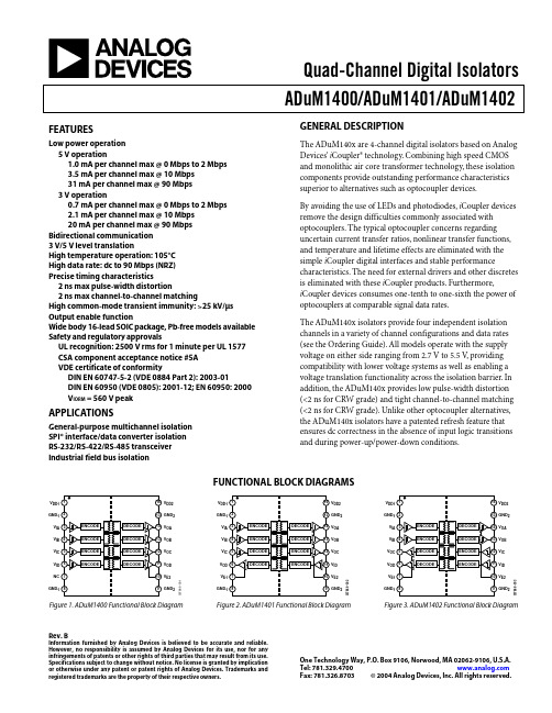
Figure 1. ADuM1400 Functional Block Diagram
03786-0-001 03786-0-002 03786-0-003
FUNCTIONAL BLOCK DIAGRAMS
VDD1 1 GND1 2
VIA 3 VIB 4 VIC 5 VOD 6 VE1 7 GND1 8
元器件交易网
Quad-Channel Digital Isolators ADuM1400/ADuM1401/ADuM1402
FEATURES
Low power operation 5 V operation 1.0 mA per channel max @ 0 Mbps to 2 Mbps 3.5 mA per channel max @ 10 Mbps 31 mA per channel max @ 90 Mbps 3 V operation 0.7 mA per channel max @ 0 Mbps to 2 Mbps 2.1 mA per channel max @ 10 Mbps 20 mA per channel max @ 90 Mbps
LM20143MH资料

January 16, 2008 LM201433A, PowerWise® Adjustable Frequency Synchronous Buck RegulatorGeneral DescriptionThe LM20143 is a full featured adjustable frequency syn-chronous buck regulator capable of delivering up to 3A of continuous output current. The current mode control loop can be compensated to be stable with virtually any type of output capacitor. For most cases, compensating the device only re-quires two external components, providing maximum flexibil-ity and ease of use. The device is optimized to work over the input voltage range of 2.95V to 5.5V making it suited for a wide variety of low voltage systems.The device features internal over voltage protection (OVP) and over current protection (OCP) circuits for increased sys-tem reliability. A precision enable pin and integrated UVLO allows the turn-on of the device to be tightly controlled and sequenced. Start-up inrush currents are limited by both an internally fixed and externally adjustable Soft-Start circuit. Fault detection and supply sequencing is possible with the integrated power good circuit.The frequency of this device can be adjusted from 500 kHz to 1.5 MHz by connecting an external resistor from the RT pin to ground.The LM20143 is designed to work well in multi-rail power supply architectures. The output voltage of the device can be configured to track a higher voltage rail using the SS/TRK pin. If the output of the LM20143 is pre-biased at startup it will not sink current to pull the output low until the internal soft-start ramp exceeds the voltage at the feedback pin.The LM20143 is offered in a 16-pin eTSSOP package with an exposed pad that can be soldered to the PCB, eliminating the need for bulky heatsinks.Features■Input voltage range 2.95V to 5.5V■Accurate current limit minimizes inductor size■97% peak efficiency■Adjustable output voltage down to 0.8V■Adjustable switching frequency (500 kHz to 1.5 MHz)■32 mΩ integrated FET switches■Starts into prebiased loads■Output voltage tracking■Peak current mode control■Adjustable Soft-Start with external capacitor■Precision enable pin with hysteresis■Integrated OVP, UVLO, power good and thermal shutdown■eTSSOP-16 exposed pad package Applications■Simple to design, high efficiency point of load regulation from a 5V or 3.3V bus■High Performance DSPs, FPGAs, ASICs and microprocessors■Broadband, Networking and Optical Communications InfrastructureTypical Application Circuit30030501 PowerWise® is a registered trademark of National Semiconductor Corporation.© 2008 National Semiconductor LM20143 3A, PowerWise ® Adjustable Frequency Synchronous Buck RegulatorConnection Diagram30030502Top VieweTSSOP-16 PackageOrdering InformationOrder Number Package Type NSC Package DrawingPackage MarkingSupplied As LM20143MH eTSSOP-16MXA16A20143MH92 Units of Rail LM20143MHE 250 Units of Tape and Reel LM20143MHX2500 Units of Tape and ReelPin DescriptionsPin #Name Description1SS/TRKSoft-Start or Tracking control input. An internal 5 µA current source charges an external capacitor to set the Soft-Start ramp rate. If driven by a external source less than 800 mV, this pin overrides the internal reference that sets the output voltage. If left open, an internal 1ms Soft-Start ramp is activated.2FBFeedback input to the error amplifier from the regulated output. This pin is connected to the inverting input of the internal transconductance error amplifier. An 800 mV reference connected to the non-inverting input of the error amplifier sets the closed loop regulation voltage at the FB pin.3PGOOD Power good output signal. Open drain output indicating the output voltage is regulating within tolerance. is recommend for most applications.4COMP External compensation pin. Connect the compensation network to resistor and capacitor to this pin to compensate the device.5NC These pins must be connected to GND to ensure proper operation.6,7PVIN Input voltage to the power switches inside the device. These pins should be connected together at the device. A low ESR capacitor should be placed near these pins to stabilize the input voltage.8,9SW Switch pin. The PWM output of the internal power switches.10,11PGND Power ground pin for the internal power switches.12EN Precision enable input for the device. An external voltage divider can be used to set the device turn-on threshold. If not used the EN pin should be connected to PVIN.13VCC Internal 2.7V sub-regulator. This pin should be bypassed with a 1 µF ceramic capacitor.14AVIN Analog input supply that generates the internal bias. Must be connected to VIN through a low pass RC filter.15AGND Quiet analog ground for the internal bias circuitry.16RT Frequency adjust pin. Connecting a resistor on this pin to ground will set the oscillator frequency.EPExposed PadExposed metal pad on the underside of the package with a weak electrical connection to ground. It is recommended to connect this pad to the PC board ground plane in order to improve heat dissipation. 2L M 20143Absolute Maximum Ratings (Note 1)If Military/Aerospace specified devices are required, please contact the National Semiconductor Sales Office/ Distributors for availability and specifications.Voltages from the indicated pins to GNDAVIN, PVIN, EN, PGOOD, SS/TRK, COMP, FB, RT-0.3V to +6V Storage Temperature-65°C to 150°C Junction Temperature150°CPower Dissipation (Note 2) 2.6W Lead Temperature (Soldering,10 sec)260°C Minimum ESD Rating (Note 3)±2kV Operating RatingsPVIN, AVIN to GND 2.95V to 5.5V Junction Temperature−40°C to + 125°CElectrical Characteristics Unless otherwise stated, the following conditions apply: AVIN = PVIN = VIN = 5V.Limits in standard type are for TJ = 25°C only, limits in bold face type apply over the junction temperature (TJ) range of -40°C to+125°C. Minimum and Maximum limits are guaranteed through test, design, or statistical correlation. Typical values represent the most likely parametric norm at TJ= 25°C, and are provided for reference purposes only.Symbol Parameter Conditions Min Typ Max UnitV FB Feedback pin voltage VIN= 2.95V to 5.5V0.7880.80.812VΔV OUT/ΔI OUT Load Regulation I OUT = 100 mA to 3A0.08%/AI CL Switch Current Limit Threshold VIN= 3.3V 4.3 4.8 5.3ARDS_ON High-Side Switch On Resistance ISW= 3.5A3655mΩRDS_ON Low-Side Switch On Resistance ISW= 3.5A3252mΩI Q Operating Quiescent Current Non-switching, VFB= VCOMP3.56mAI SD Shutdown Quiescent current VEN= 0V90180µAV UVLO VIN Under Voltage Lockout Rising VIN2.45 2.7 2.95VVUVLO_HYS VIN Under Voltage Lockout Hysteresis Falling VIN45100mVV VCC VCC Voltage IVCC= 0 µA 2.45 2.7 2.95VI SS Soft-Start Pin Source Current VSS/TRK= 0V2 4.57µAV TRACK SS/TRK Accuracy, VSS- VFBVSS/TRK= 0.4V-10315mVOscillatorF OSCH Oscillator Frequency RT= 49.9 kΩ135015001650kHzF OSCL Oscillator Frequency RT= 249 kΩ450510570kHzDCMAX Maximum Duty Cycle ILOAD= 0A85%TON_TIMEMinimum On Time100nsTCL_BLANK Current Sense Blanking Time After Rising VSW80nsError Amplifier and ModulatorI FB Feedback pin bias current VFB= 0.8V1100nAICOMP_SRC COMP Output Source Current VFB= VCOMP= 0.6V80100µAICOMP_SNK COMP Output Sink Current VFB= 1.0V, VCOMP= 0.6V80100µAGm Error Amplifier Transconductance ICOMP= ± 50 µA450510600µmhoAVOLError Amplifier Voltage Gain2000V/V Power GoodV OVP Over Voltage Protection Rising Threshold With respect to VFB105108111%VOVP_HYSOver Voltage Protection Hysteresis23%V PGTH PGOOD Rising Threshold With respect to VFB929496%VPGHYSPGOOD Falling Hysteresis23%TPGOODPGOOD deglitch time16µsI OL PGOOD Low Sink Current VPGOOD= 0.4V0.61mAI OH PGOOD High Leakage Current VPGOOD= 5V5100nALM20143Symbol ParameterConditionsMinTypMaxUnitEnableV IH_EN EN Pin turn-on Threshold V EN Rising 1.08 1.18 1.28V V EN_HYS EN Pin Hysteresis 66 mV Thermal ShutdownT SD Thermal Shutdown160 °C T SD_HYS Thermal Shutdown Hysteresis 10 °C Thermal ResistanceθJAJunction to Ambient38°C/WNote 1:Absolute Maximum Ratings indicate limits beyond which damage to the device may occur. Operating Ratings indicate conditions for which the device is intended to be functional, but do not guarantee specific performance limits. For guaranteed specifications and test conditions, see the Electrical Characteristics.Note 2:The maximum allowable power dissipation is a function of the maximum junction temperature, T J_MAX , the junctions-to-ambient thermal resistance, θJA ,and the ambient temperature, T A . The maximum allowable power dissipation at any ambient temperature is calculated using: P D_MAX = (T J_MAX – T A )/θJA . The maximum power dissipations of 2.6W is determined using T A = 25°C, θJA = 38°C/W, and T J_MAX = 125°C.Note 3:The human body model is a 100 pF capacitor discharged through a 1.5 k Ω resistor to each pin.Typical Performance CharacteristicsUnless otherwise specified: C IN = C OUT = 100 µF, L = 1.0 µH(Coilcraft MSS1038), V IN = 5V, V OUT = 1.2V, R LOAD = 1.2Ω, f SW = 1 MHz, T A = 25°C for efficiency curves, loop gain plots and waveforms, and T J = 25°C for all others.Efficiency vs. Load Current (V IN = 5V, f SW = 1.5 MHz)30030531Efficiency vs. Load Current (V IN = 3.3V, f SW = 1.5 MHz)30030530Efficiency vs. Load Current (V IN = 5V, f SW = 1.0 MHz)30030547Efficiency vs. Load Current (V IN = 3.3V, f SW = 1.0 MHz)30030546 4L M 20143Efficiency vs. Load Current (V IN = 5.0V, f SW = 500 kHz)30030549Efficiency vs. Load Current (V IN = 3.3V, f SW = 500 kHz)30030548High-Side FET Resistance vs. Temperature 30030557Low-Side FET Resistance vs. Temperature30030558Error Amplifier Gain vs. Frequency 30030536Line Regulation30030537LM20143Load Regulation30030538Feedback Pin Voltage vs. Temperature30030551Switching Frequency vs. Temperature30030539Switching Frequency vs. R T30030550Quiescent Current vs. V IN (Not Switching)30030540Shutdown Current vs. Temperature30030541 6L M 20143Enable Threshold vs. Temperature30030528UVLO Threshold vs. Temperature30030545Peak Current Limit vs. Temperature30030542Peak Current Limit vs. V OUT30030554Peak Current Limit vs. V IN30030555Load Transient Response30030534LM20143Line Transient Response30030543Start Up (Soft-Start)30030544Start Up (Tracking)30030533Short Circuit Input Current vs. V IN30030556Power Down30030532 8L M 20143Block Diagram30030503 LM20143Operation DescriptionGENERALThe LM20143 switching regulator features all of the functions necessary to implement an efficient low voltage buck regula-tor using a minimum number of external components. This easy to use regulator features two integrated switches and is capable of supplying up to 3A of continuous output current.The regulator utilizes peak current mode control with nonlin-ear slope compensation to optimize stability and transient response over the entire output voltage range. Peak current mode control also provides inherent line feed-forward, cycle-by-cycle current limiting and easy loop compensation. The switching frequency can be varied from 500 kHz to 1.5 MHz with an external resistor to ground. The device can operate at high switching frequency allowing use of a small inductor while still achieving efficiencies as high as 96%. The precision internal voltage reference allows the output to be set as low as 0.8V. Fault protection features include: current limiting,thermal shutdown, over voltage protection, and shutdown ca-pability. The device is available in the eTSSOP-16 package featuring an exposed pad to aid thermal dissipation. The LM20143 can be used in numerous applications to efficiently step-down from a 5V or 3.3V bus. The typical application cir-cuit for the LM20143 is shown in Figure 2 in the design guide.PRECISION ENABLEThe enable (EN) pin allows the output of the device to be en-abled or disabled with an external control signal. This pin is a precision analog input that enables the device when the volt-age exceeds 1.2V (typical). The EN pin has 100 mV of hys-teresis and will disable the output when the enable voltage falls below 1.1V (typical). If the EN pin is not used, it should be connected to VIN. Since the enable pin has a precise turn-on threshold it can be used along with an external resistor divider network from V IN to configure the device to turn-on at a precise input voltage. The precision enable circuitry will re-main active even when the device is disabled.PEAK CURRENT MODE CONTROLI n most cases, the peak current mode control architecture used in the LM20143 only requires two external components to achieve a stable design. The compensation can be select-ed to accommodate any capacitor type or value. The external compensation also allows the user to set the crossover fre-quency and optimize the transient performance of the device.For duty cycles above 50% all current mode control buck converters require the addition of an artificial ramp to avoid sub-harmonic oscillation. This artificial linear ramp is com-monly referred to as slope compensation. What makes the LM20143 unique is the amount of slope compensation will change depending on the output voltage. When operating at high output voltages the device will have more slope com-pensation than when operating at lower output voltages. This is accomplished in the LM20143 by using a non-linear parabolic ramp for the slope compensation. The parabolic slope compensation of the LM20143 is much better than the traditional linear slope compensation because it optimizes the stability of the device over the entire output voltage range.CURRENT LIMITThe precise current limit of the LM20143 is set at the factory to be within 10% over the entire operating temperature range.This enables the device to operate with smaller inductors that have lower saturation currents. When the peak inductor cur-rent reaches the current limit threshold, an over current event is triggered and the internal high-side FET turns off and thelow-side FET turns on allowing the inductor current to ramp down until the next switching cycle. For each sequential over-current event, the reference voltage is decremented and PWM pulses are skipped resulting in a current limit that does not aggressively fold back for brief over-current events, while at the same time providing frequency and voltage foldback protection during hard short circuit conditions.SOFT-START AND VOLTAGE TRACKINGThe SS/TRK pin is a dual function pin that can be used to set the start up time or track an external voltage source. The start up or Soft-Start time can be adjusted by connecting a capac-itor from the SS/TRK pin to ground. The Soft-Start feature allows the regulator output to gradually reach the steady state operating point, thus reducing stresses on the input supply and controlling start up current. If no Soft-Start capacitor is used the device defaults to the internal Soft-Start circuitry re-sulting in a start up time of approximately 1 ms. For applica-tions that require a monotonic start up or utilize the PGOOD pin, an external Soft-Start capacitor is recommended. The SS/TRK pin can also be set to track an external voltage source. The tracking behavior can be adjusted by two external resistors connected to the SS/TRK pin as shown in Figure 7.in the design guide.PRE-BIAS START UP CAPABILITYThe LM20143 is in a pre-biased state when the device starts up with an output voltage greater than zero. This often occurs in many multi-rail applications such as when powering an FP-GA, ASIC, or DSP. In these applications the output can be pre-biased through parasitic conduction paths from one sup-ply rail to another. Even though the LM20143 is a syn-chronous converter it will not pull the output low when a pre-bias condition exists. During start up the LM20143 will not sink current until the Soft-Start voltage exceeds the voltage on the FB pin. Since the device can not sink current it protects the load from damage that might otherwise occur if current is conducted through the parasitic paths of the load.POWER GOOD AND OVER VOLTAGE FAULT HANDLING The LM20143 has built in under and over voltage compara-tors that control the power switches. Whenever there is an excursion in output voltage above the set OVP threshold, the part will terminate the present on-pulse, turn-on the low-side FET, and pull the PGOOD pin low. The low-side FET will re-main on until either the FB voltage falls back into regulation or the zero cross detection is triggered which in turn tri-states the FETs. If the output reaches the UVP threshold the part will continue switching and the PGOOD pin will be asserted and go low. Typical values for the PGOOD resistor are on the or-der of 100 k Ω or less. To avoid false tripping during transient glitches the PGOOD pin has 16 µs of built in deglitch time to both rising and falling edges.UVLOThe LM20143 has a built-in under-voltage lockout protection circuit that keeps the device from switching until the input voltage reaches 2.7V (typical). The UVLO threshold has 45mV of hysteresis that keeps the device from responding to power-on glitches during start up. If desired the turn-on point of the supply can be changed by using the precision enable pin and a resistor divider network connected to V IN as shown in Figure 6. in the design guide.THERMAL PROTECTIONInternal thermal shutdown circuitry is provided to protect the integrated circuit in the event that the maximum junction tem-10L M 20143perature is exceeded. When activated, typically at 160°C, the LM20143 tri-states the power FETs and resets soft start. After the junction cools to approximately 150°C, the part starts up using the normal start up routine. This feature is provided to prevent catastrophic failures from accidental device over-heating.LIGHT LOAD OPERATIONThe LM20143 offers increased efficiency when operating at light loads. Whenever the load current is reduced to a point where the peak to peak inductor ripple current is greater than two times the load current, the part will enter the diode emu-lation mode preventing significant negative inductor current.The point at which this occurs is the critical conduction bound-ary and can be calculated by the following equation:Several diagrams are shown in Figure 1 illustrating continu-ous conduction mode (CCM), discontinuous conduction mode, and the boundary condition.It can be seen that in diode emulation mode, whenever the inductor current reaches zero the SW node will become high impedance. Ringing will occur on this pin as a result of the LC tank circuit formed by the inductor and the parasitic capaci-tance at the node. If this ringing is of concern an additional RC snubber circuit can be added from the switch node to ground.At very light loads, usually below 100 mA, several pulses may be skipped in between switching cycles, effectively reducing the switching frequency and further improving light-load effi-ciency.30030505FIGURE 1. Modes of Operation for LM20143LM20143Design GuideThis section walks the designer through the steps necessaryto select the external components to build a fully functionalpower supply. As with any DC-DC converter numerous trade-offs are possible to optimize the design for efficiency, size, orperformance. These will be taken into account and highlight-ed throughout this discussion. To facilitate component selec-tion discussions the circuit shown in Figure 2 below may beused as a reference. Unless otherwise indicated all formulasassume units of amps (A) for current, farads (F) for capaci-tance, henries (H) for inductance and volts (V) for voltages.30030523FIGURE 2. Typical Application CircuitThe first equation to calculate for any buck converter is duty-cycle. Ignoring conduction losses associated with the FETsand parasitic resistances it can be approximated by:INDUCTOR SELECTION (L)The inductor value is determined based on the operating fre-quency, load current, ripple current, and duty cycle.The inductor selected should have a saturation current ratinggreater than the peak current limit of the device. Keep in mindthe specified current limit does not account for delay of thecurrent limit comparator, therefore the current limit in the ap-plication may be higher than the specified value. To optimizethe performance and prevent the device from entering currentlimit at maximum load, the inductance is typically selectedsuch that the ripple current, ΔiL, is less than 30% of the ratedoutput current. Figure 3, shown below illustrates the switchand inductor ripple current waveforms. Once the input volt-age, output voltage, operating frequency, and desired ripplecurrent are known, the minimum value for the inductor can becalculated by the formula shown below:30030509FIGURE 3. Switch and Inductor Current WaveformsIf needed, slightly smaller value inductors can be used, how-ever, the peak inductor current, IOUT+ Δi L/2, should be keptbelow the peak current limit of the device. In general, the in-ductor ripple current, ΔiL, should be greater than 10% of therated output current to provide adequate current sense infor-mation for the current mode control loop. If the ripple currentin the inductor is too low, the control loop will not have suffi-cient current sense information and can be prone to instability.OUTPUT CAPACITOR SELECTION (COUT)The output capacitor, COUT, filters the inductor ripple currentand provides a source of charge for transient load conditions.A wide range of output capacitors may be used with theLM20143 that provide excellent performance. The best per-formance is typically obtained using ceramic, SP, or OSCONtype chemistries. Typical trade-offs are that the ceramic ca-pacitor provides extremely low ESR to reduce the outputripple voltage and noise spikes, while the SP and OSCONcapacitors provide a large bulk capacitance in a small volumefor transient loading conditions.When selecting the value for the output capacitor the two per-formance characteristics to consider are the output voltageripple and transient response. The output voltage ripple canbe approximated by using the formula shown below.Where, ΔVOUT(V) is the amount of peak to peak voltage rippleat the power supply output, RESR(Ω) is the series resistanceof the output capacitor, fSW(Hz) is the switching frequency,and COUT(F) is the output capacitance used in the design.The amount of output ripple that can be tolerated is applica-tion specific; however a general recommendation is to keepthe output ripple less than 1% of the rated output voltage.Keep in mind ceramic capacitors are sometimes preferredbecause they have very low ESR; however, depending onpackage and voltage rating of the capacitor the value of thecapacitance can drop significantly with applied voltage. Theoutput capacitor selection will also affect the output voltagedroop during a load transient. The peak droop on the outputvoltage during a load transient is dependent on many factors;however, an approximation of the transient droop ignoringloop bandwidth can be obtained using the following equation.12LM2143Where, COUT(F) is the minimum required output capacitance,L (H) is the value of the inductor, VDROOP(V) is the outputvoltage drop ignoring loop bandwidth considerations, ΔIOUT-STEP(A) is the load step change, RESR(Ω) is the outputcapacitor ESR, VIN(V) is the input voltage, and VOUT(V) isthe set regulator output voltage. Both the tolerance and volt-age coefficient of the capacitor needs to be examined whendesigning for a specific output ripple or transient drop target.INPUT CAPACITOR SELECTION (CIN)Good quality input capacitors are necessary to limit the ripplevoltage at the VIN pin while supplying most of the switch cur-rent during the on-time. In general it is recommended to usea ceramic capacitor for the input as they provide both a lowimpedance and small footprint. One important note is to usea good dielectric for the ceramic capacitor such as X5R orX7R. These provide better over temperature performanceand also minimize the DC voltage derating that occurs on Y5Vcapacitors. For most applications, a 22 µF, X5R, 6.3V inputcapacitor is sufficient; however, additional capacitance maybe required if the connection to the input supply is far from thePVIN pins. The input capacitor should be placed as close aspossible PVIN and PGND pins of the device.Non-ceramic input capacitors should be selected for RMScurrent rating and minimum ripple voltage. A good approxi-mation for the required ripple current rating is given by therelationship:As indicated by the RMS ripple current equation, highest re-quirement for RMS current rating occurs at 50% duty cycle.For this case, the RMS ripple current rating of the input ca-pacitor should be greater than half the output current. For bestperformance, low ESR ceramic capacitors should be placedin parallel with higher capacitance capacitors to provide thebest input filtering for the device.SETTING THE OUTPUT VOLTAGE (RFB1, RFB2)The resistors RFB1and RFB2are selected to set the outputvoltage for the device. Table 1, shown below, provides sug-gestions for RFB1and RFB2for common output voltages.TABLE 1. Suggested Values for RFB1and RFB2RFB1(kΩ)RFB2(kΩ)V OUTshort open0.84.9910 1.28.8710.2 1.512.710.2 1.821.510.2 2.531.610.2 3.3If different output voltages are required, RFB2should be se-lected to be between 4.99 kΩ to 49.9 kΩ and RFB1can becalculated using the equation below.ADJUSTING THE OPERATING FREQUENCY (RT)The operating frequency of the LM20143 can be adjusted byconnecting a resistor from the RT pin to ground. The equationshown below can be used to calculate the value of RTfor agiven operating frequency.Where, fSWis the switching frequency in kHz, and RTis thefrequency adjust resistor in kΩ. Please refer to the curve Os-cillator Frequency verses RTin the typical performance char-acteristics section. If the RTresistor is omitted the device willnot operate.LOOP COMPENSATION (RC1, CC1)The purpose of loop compensation is to meet static and dy-namic performance requirements while maintaining adequatestability. Optimal loop compensation depends on the outputcapacitor, inductor, load, and the device itself. Table 2 belowgives values for the compensation network that will result ina stable system when using a 100 µF, 6.3V ceramic X5R out-put capacitor and 1 µH inductor.TABLE 2. Recommended Compensation forCOUT= 100 µF, L = 1 µH & fSW= 1 MHzVINVOUTCC1(nF)RC1(kΩ)5.00 3.30 4.717.85.00 2.50 4.712.15.00 1.80 4.77.685.00 1.50 4.7 5.95.00 1.20 4.7 3.575.000.80 4.7 1.583.30 2.504.7133.30 1.804.79.763.30 1.504.7 6.493.30 1.204.7 4.643.300.804.7 1.58If the desired solution differs from the table above the looptransfer function should be analyzed to optimize the loopcompensation. The overall loop transfer function is the prod-uct of the power stage and the feedback network transferfunctions. For stability purposes, the objective is to have aloop gain slope that is -20db/decade from a very low frequen-cy to beyond the crossover frequency. Figure 4, shown below,shows the transfer functions for power stage, feedback/com-pensation network, and the resulting closed loop system forthe LM20143.LM20143。
M1A3P600-PQ144PP中文资料(Actel)中文数据手册「EasyDatasheet - 矽搜」

•差分I / O标准:LVPECL,LVDS,B-LVDS,和
M-LVDS(A3P250及以上)
•I / O寄存器输入,输出,并启用路径 •支持热插拔,冷饶让I / O •可编程输出摆率
‡ † 和驱动强度
•弱上拉/ -Down
•IEEE 1149.1(JTAG)边界扫描测试
•引脚兼容横跨ProASIC3系列套餐
169
1.0 1.45
FG256 17 × 17
289
1.0 1.60
FG484 23 × 23
529
1.0 2.23
II
v1.0
芯片中文手册,看全文,戳
ProASIC3订购信息
闪存ProASIC3系列FPGA
A3P1000 _ 1
FG
G
144
I
封装引脚数
应用程序(温度范围)
空白=商业(0°C至+ 70°C环境温度下)
A3P600 = 60万系统门 A3P1000 = 1,000,000个系统门
ProASIC3器件与 ARM7
M7A3P1000 = 1,000,000个系统门
ProASIC3器件具有 Cortex-M1
M1A3P250 = 250000系统门
M1A3P400 = 400000系统门 M1A3P600 = 600000个系统门 M1A3P1000 = 百万个系统门
* 为-F速度等级目标DC和开关特性只是基于模拟. 规定-F速度等级特点是主题建立FPGA规格后更改.一些限制可能会增加,并会反映在该文档后续版本.该-F速度等 级只在商用温度范围内支持.
v1.0
III
芯片中文手册,看全文,戳
温度等级奉献
包裹
MPSW42中文资料

CASE 29–05, STYLE 1 TO–92 (TO–226AE)
THERMAL CHARACTERISTICS
Characteristic Thermal Resistance, Junction to Ambient Thermal Resistance, Junction to Case Symbol RqJA RqJC Max 125 50 Unit °C/W °C/W
v 300 ms, Duty Cycle v 2.0%.
Preferred devices are Motorola recommended choices for future use and best overall value.
Motorola Small–Signal Transistors, FETs and Diodes Device Data © Motorola, Inc. 1996
Motorola Preferred Device
1
2
1 EMITTER
3
MAXIMUM RATINGS
Rating Collector – Emitter Voltage Collector – Base Voltage Emitter – Base Voltage Collector Current — Continuous Total Device Dissipation @ TA = 25°C Derate above 25°C Total Device Dissipation @ TC = 25°C Derate above 25°C Operating and Storage Junction Temperature Range Symbol VCEO VCBO VEBO IC PD PD TJ, Tstg Value 300 300 6.0 500 1.0 8.0 2.5 20 – 55 to +150 Unit Vdc Vdc Vdc mAdc Watt mW/°C Watts mW/°C °C
ADUM1410ARWZ中文资料
06580-002
APPLICATIONS
General-purpose multichannel isolation SPI interface/data converter isolation RS-232/RS-422/RS-485 transceivers Industrial field bus isolation
元器件交易网
Quad-Channel Digital Isolators ADuM1410/ADuM1411/ADuM1412
FEATURES
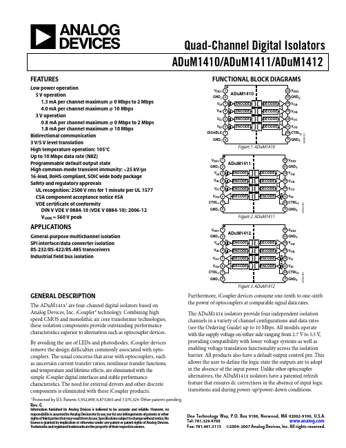
FUNCTIONAL BLOCK DIAGRAMS
06580-001
Low power operation 5 V operation 1.3 mA per channel maximum @ 0 Mbps to 2 Mbps 4.0 mA per channel maximum @ 10 Mbps 3 V operation 0.8 mA per channel maximum @ 0 Mbps to 2 Mbps 1.8 mA per channel maximum @ 10 Mbps
元器件交易网
ADuM1410/ADuM1411/ADuM1412
TABLE OF CONTENTS
Features .............................................................................................. 1
Electrical Characteristics—3 V Operation................................ 5
Electrical Characteristics—Mixed 5 V/3 V or 3 V/5 V Operation....................................................................................... 7
M1A3P250-2VQ100IVQ100中文资料(Microsemi)中文数据手册「EasyDatasheet - 矽搜」

版本
器件手册章节可以有不同版本号. Actel目标是为客户提供及时事项最新信息.其结果是,该 表数据之前公布 已被充分表征.数据表被指定为"产品简介","高级",并 "生产".这些类别定义如下:
产品简介
产品简介是一个数据表摘要版本(高级或生产),包含 一般产品信息.本文给出具体设备和家庭概况 信息.
I / O说明和使用方法
I/在IGLOO和ProASIC3器件O结构. . . . . . . . . . . . . . . . . . . . . . . . . . . . . . . . . . . . . . . . . . . .7-1 I / O软件控制在低功耗闪存设备. . . . . . . . . . . . . . . . . . . . . . . . . . . . . . . . . . . . . . . . .8-1 DDR为Actel低功耗闪存设备. . . . . . . . . . . . . . . . . . . . . . . . . . . . . . . . . . . . . . . . . . . . . . . .9-1
封装和引脚说明 引脚说明. . . . . . . . . . . . . . . . . . . . . . . . . . . . . . . . . . . . . . . . . . . . . . . . . . . . . . . . . . . . . . . . . . .10-1 包装. . . . . . . . . . . . . . . . . . . . . . . . . . . . . . . . . . . . . . . . . . . . . . . . . . . . . . . . . . . . . . . . . . . . . . .11-1
最新MPS使用说明书(西门子)

M P S使用说明书(西门子)FMS使用说明书一、产品概述:随着现代科技的日新月异,自动化生产线作为能实现产品生产过程自动化的一种机器体系,现代生产企业竞争的重要手段,扮演着越来越重要的角色。
所谓的自动化生产线,即通过采用一套能自动进行加工、检测、装卸运输的机器设备,组成高度连续的、完全自动化的生产线,来实现产品的生产。
是在连续流水线基础上进一步发展形成的,是一种先进的生产组织形式。
它的发展趋势是:提高可调性,扩大工艺范围,提高加工精度和自动化程序,同计算机结合实现整体自动化车间与自动化工厂。
与此同时,社会对自动化职业技能人才的日益见长,结合我们的当前社会需求和教学的需求,我公司的FMS模块话自动化设备应运而生。
其主要特色:一、灵活性:我公司FMS以其模块化大大的提高了其灵活性,更贴近现实生产实际过程,让学生在学校就能够了解实际生产实践的细节,填补了产学同步的空白。
二、综合性:我公司产品综合了现代实际生产中较流行的较先进的各种很实用的技术知识点,其中包括PLC控制编程技术,ProfiBus网络通讯技术,电气控制技术,气动应用技术,传感器技术,步进驱动控制技术,机器人应用技术等几大主要知识点。
三、创新性:由于采用了模块化的设计,学生可以发挥自己的创新思维,对原有的生产流程进行创新改造。
在掌握基础知识的前提下,进一步提高学生的积极性、动手能力和创新思维,为将来的就业和实现自己的人生价值打下坚实的基础。
综上可知,我司的FMS产品不但融合了现代先进的技术知识点,而且根据社会发展和教学的需要采用了较先进的设计理念。
本产品主要相关教材有《模块化生产加工系统应用教程》、《模块化生产加工系统应用技术》、《典型自动化设备及生产线应用与维护》等,适合广大中职、高职院校、技能鉴定机构单位等进行自动化方向的培训和教学等场合。
二、产品构成及参数:(1) MPS系统构成我司SX-815A-III FMS柔性自动化由计算机系统单元、主站网络单元、供料单元、上下机械手单元、气动搬运单元、模拟加工单元、图像检测单元、成品装配单元、机器人单元、成品分拣单元、环形传送单元、立体仓库单元和分类网络监控单元等组成。
联拓辉 LTH1410 2A 降压、开关型PWM DC DC 稳压器 数据手册

2A 降压、开关型PWM DC/DC 稳压器LTH1410LTH1410数据手册基本描述:LTH1410是一个由内部功率MOSFET 单片集成降压(buck )稳压器,达到2A 的连续输出。
电流可以在大范围的电源输入下有很好的负载能力和线性调节能力。
电流型实现了快速的暂态过程和提高回路的稳定性。
故障保护包括了一个循环电流限制和过热保护,小于20微安的关断电流。
LTH1410要求一个最小数量的容易使用的标准外围组件。
同步引脚允许这部分驱动600kHz 电路。
特性:�2A 的输出电流�0.18Ω的内部开关型MOSFET 内阻�稳定的低ESR 输出陶瓷电容�高达90%功效�低于20μA 的关断电流�400kHz 的固定频率�过热保护�循环过电流保护� 4.75V 至15V 的工作输入范围�输出电压调整:1.28V 至13V �可设计的欠电压保护�与输入频率同步�8引脚SO 封装应用:�DVD ,车载电器,GPS �分散功率系统�通信产品�计算机(网卡,调制解调器,监视器,主板,声卡……)�电池充电器,电话,数据库,LED 显示器,卫星接收器2A降压、开关型PWM DC/DC稳压器典型应用电路:LTH1410功效vs.输出电压&输出电流(V IN=10V)系统框图:LTH1410BLOCK DIAGRAM功能描述:LTH1410是一个电流型稳压器,也就是说,补偿引脚的电压与流过负载的电流成比例。
在开始时,上面的晶体管M1是断开的,下面的晶体管M2是闭合的,V C引脚的电压比电流检测放大器的输出更高,电流比较器的输出是低电平,400kHz时钟信号的上升沿使RS触发。
它的输出使M2断开,使M1闭合,从而使开关引脚和电感与输入电源连接。
增大的电感电流被电流检测放大器检测并且放大。
电流比较器用来比较被电流检测放大器输出的斜波补偿电流与误差放大器的输出。
当电流检测放大器的值加上斜波补偿信号超过Comp引脚电压时,RS触发器复位并且芯片恢复到最初M1断开,M2闭合的状态,反之,如果电流检测放大器的值加上斜波补偿信号没有超过Comp引脚的电压,那么,时钟信号的下降沿将会使触发信号复位。
mps430G2553中文资料

时钟
I/O 封装类型
16
512 2x TA3
8
8
512 2x TA3
8
4
256 2x TA3
8
2
256 2x TA3
8
1
256 2x TA3
8
24
32 引脚 QFN 封装
28 引脚
24 TSSOP 封
LF,
装
-
1
DCO,
VLO
20 引脚
16 TSSOP 封
装
16
20 引脚 PDIP 封装
24
32 引脚 QFN 封装
引导加 载器 (BSL)
嵌入式 仿真模
块 (EEM)
1
1
1
1
1
1
1
1
1
1
表 1. 提供的选项(1)(2) (接下页)
ZHCS178E – APRIL 2011 – REVISED JANUARY 2012
闪存 (KB)
RAM (B)
Timer_A
COMP_A+ 通道
10 通道 ADC
USCI A0/B0
典型应用包括低成本传感器系统,此类系统负责捕获模拟信号、将之转换为数字值、随后对数据进行处理以进行显 示或传送至主机系统。
1
Please be aware that an important notice concerning availability, standard warranty, and use in critical applications of Texas Instruments semiconductor products and disclaimers thereto appears at the end of this data sheet.
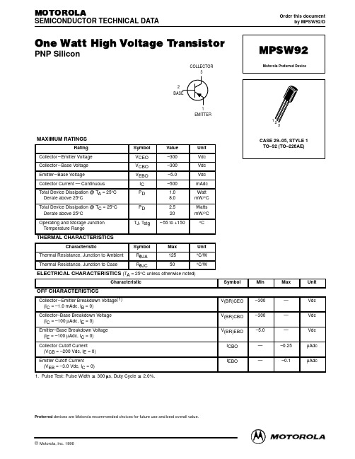
MPSW92中文资料
SMALL–SIGNAL CHARACTERISTICS
Current–Gain — Bandwidth Product (IC = –10 mAdc, VCE = –20 Vdc, f = 20 MHz) Collector–Base Capacitance (VCB = –20 Vdc, IE = 0, f = 1.0 MHz) 1. Pulse Test: Pulse Width fT Ccb 50 — — 6.0 MHz pF
Ceb
TJ = 25°C
30 20
Ccb
–5.0 –10
–20
–50 –100 –200
10 –1.0
–2.0 –3.0
–5.0 –7.0 –10
–20 –30
–50 –70 –100
VR, REVERSE VOLTAGE (VOLTS)
IC, COLLECTOR CURRENT (mA)
Figure 5. Capacitance
v 300 ms, Duty Cycle v 2.0%.
Preferred devices are Motorola recommended choices for future use and best overall value.
Motorola Small–Signal Transistors, FETs and Diodes Device Data © Motorola, Inc. 1996
Figure 1. DC Current Gain
Figure 2. Collector Saturation Region
2
Motorola Small–Signal Transistors, FETs and Diodes Device Data
ADUM1400英文芯片资料

ADuM1400/1/2
0~2Mbps 时 1401 工作电流 0~2Mbps 时 1402 工作电流 输入电平 IDD1 IDD2 IDD1 IDD2 VIH VIL 输出电平 VOH VOL 最大输出电流 IO1(side1) IO2(side2) VDD1=VDD2=3V,TA=25℃ 工作参数 工作电压 符号 VDD1 VDD2 静态工作电流 IDDI(Q) IDDO(Q) 0~2Mbps 时 1400 工作电流 0~2Mbps 时 1401 工作电流 0~2Mbps 时 1402 工作电流 输入电平 IDD1 IDD2 IDD1 IDD2 IDD1 IDD2 VIH VIL 输出电平 VOH VOL 最大输出电流 IO1(side1) IO2(side2) -18 -22 VDD1,2-0.1 3.0 0.0 0.1 18 22 1.6 0.4 Min 2.7 2.7 Typ 3.0 3.0 0.26 0.11 1.2 0.5 1.0 0.7 0.9 0.9 Max 3.6 3.6 0.31 0.14 1.9 0.9 1.6 1.2 1.5 1.5 单位 V V mA mA mA mA mA mA mA mA V V V V mA mA -18 -22 VDD1,2-0.1 5.0 0.0 0.1 18 22 2.0 0.8 1.8 1.2 1.5 1.5 2.4 1.8 2.1 2.1 mA mA mA mA V V V V mA mA
功能描述 Side1 端供电电源(2.7V~5.5V) Side1 端电源地 Side1 逻辑输入 A Side1 逻辑输入 B Side1 逻辑输出 C Side1 逻辑输出 D Side2 端供电电源(2.7V~5.5V) Side2 端电源地 Side2 逻辑输出 A Side2 逻辑输出 B Side2 逻辑输入 C Side2 逻辑输入 D 输出使能 1 脚 当 VE1 为高或悬空时,VOC,VOD 输出有效 当 VE1 为低时,VOC,VOD 输出禁止 输出使能 2 脚 当 VE2 为高或悬空时,VOA,VOB 输出有效 当 VE2 为低时,VOA,VOB 输出禁止
MPSA14中文资料
元器件交易网
DISCRETE SEMICONDUCTORS
DATA SHEET
book, halfpage
M3D186
MPSA14 NPN Darlington transistor
Product specification Supersedes data of 1997 Apr 24
OUTLINE
VERSION
IEC
REFERENCES
JEDEC
EIAJ
EUROPEAN PROJECTION
SOT54
TO-92
SC-43
ISSUE DATE 97-02-28
1999 Apr 27
4
元器件交易网
Philips Semiconductors
NPN Darlington transistor
APPLICATIONS • High gain amplification.
DESCRIPTION NPN Darlington transistor in a TO-92; SOT54 plastic package. PNP complement: MPSA64.
PINNING
PIN 1 2 3
Application information
M1A3P400-FFGG144中文资料(Actel)中文数据手册「EasyDatasheet - 矽搜」

* 为-F速度等级目标DC和开关特性只是基于模拟. 规定-F速度等级特点是主题建立FPGA规格后更改.一些限制可能会增加,并会反映在该文档后续版本.该-F速度等 级只在商用温度范围内支持.
v1.0
III
芯片中文手册,看全文,戳
温度等级奉献
包裹
A3P015 A3P030
ARM7设 备
在零件号"G". 6. M1A3P250设备不支持FG256或QN132包.
表 1-1•
ProASIC3 FPGA包装规格尺寸
包裹
QN68
长 ×宽
8×8
(毫米 \毫米)
标称面产品
64
(mm 2)
间距( mm)
0.4
高度( mm)
0.90
QN132 8×8
64
0.5 0.75
VQ100 14 × 14
• 单芯片解决方案
• 防护留编程设计时已关闭
高性能
•350 MHz系统性能
•3.3 V,66 MHz64位PCI
†
在系统编程( ISP)和安全性
•安全ISP使用片上128位高级加密
标准(AES)解密(除ARM功能ProASIC
通过JTAG器件)(IEEE 1532兼容)
†
• FlashLock ® 以安全FPGA内容
A3P600 = 60万系统门 A3P1000 = 1,000,000个系统门
ProASIC3器件与 ARM7
M7A3P1000 = 1,000,000个系统门
ProASIC3器件具有 Cortex-M1
M1A3P250 = 250000系统门
M1A3P400 = 400000系统门 M1A3P600 = 600000个系统门 M1A3P1000 = 百万个系统门
ADUM1410_1411_1412_cn中文资料

受美国专利5,952,849号、6,873,065号、6,903,578号和7,075,329号保护。 Document Feedback
Rev. J
Information furnished by Analog Devices is believed to be accurate and reliable. However, no responsibility is assumed by Analog Devices for its use, nor for any infringements of patents or other rights of third parties that may result from its use. Speci cations subject to change without notice. No license is granted by implication or otherwise under any patent or patent rights of Analog Devices. Trademarks and registered trademarks are the property of their respective owners.
修订历史
2014年4月—修订版I至修订版J 更改表5 ......................................................................................... 10 2012年3月—修订版H至修订版I 为特性部分的“安全和法规认证”创建超链接 ........................ 1 更改印刷电路板布局部分 ........................................................ 19 2010年11月—修订版G至修订版H 特性部分增加TÜV认证 .............................................................. 1 表5增加TÜV栏 ............................................................................ 10 2007年6月—修订版F至修订版G 全面更新VDE认证 ....................................................................... 1 更改特性和应用部分 ................................................................... 1 更改表1中的直流规格 ................................................................. 3 更改表2中的直流规格 ................................................................. 5 更改表3中的直流规格 ................................................................. 7 更改法规信息部分 ..................................................................... 10 增加表10 ....................................................................................... 12 增加隔离寿命部分 ..................................................................... 21 2007年2月—修订版E至修订版F 增加ADuM1410ARWZ .......................................................... 通篇 引脚名称CTRL统一更新为CTRL2............................................ 1 更改订购指南 .............................................................................. 21 2006年10月—修订版D至修订版E 增加ADuM1411和ADuM1412 ............................................. 通篇 删除ADuM1310....................................................................... 通篇 更改“特性”...................................................................................... 1 更改技术规格部分 ....................................................................... 3 更新外形尺寸 .............................................................................. 20 更改“订购指南”............................................................................20 2006年3月—修订版C至修订版D 增加注释1并更改图2 ................................................................... 1 更改绝对最大额定值 ................................................................. 11 2005年11月—修订版C:初始版065Biblioteka 0-001CTRL2 GND2
MPS_MP1470规格书
HSRDS-ON LSRDS-ON SWLKG ILIMIT fSW VFB=0.75V DMAX VFB=700mV τON_MIN VFB VEN_RISING VEN_FALLING IEN INUVVth INUVHYS τSS VEN=2V VEN=0
1 3 400 88 776 1.4 1.23 3.7 490 92 90 800 1.5 1.32 1.6 0 3.85 4.2 340 1 150 20 4.55 580
824 1.6 1.41
V mV ms °C °C
MP1470 Rev. 1.02 8/27/2013
MPS Proprietary Information. Patent Protected. Unauthorized Photocopy and Duplication Prohibited. © 2013 MPS. All Rights Reserved.
MP1470 Rev. 1.02 8/27/2013
MPS Proprietary Information. Patent Protected. Unauthorized Photocopy and Duplication Prohibited. © 2013 MPS. All Rights Reserved.
The MP1470 requires a minimal number of readily-available, standard, external components and is available in a space-saving 6-pin TSOT23 package.
APPLICATIONS
MPS Proprietary Information. Patent Protected. Unauthorized Photocopy and Duplication Prohibited. © 2013 MPS. All Rights Reserved.
MPSW63中文资料
SMALL–SIGNAL CHARACTERISTICS
Current–Gain — Bandwidth Product(2) (IC = –10 mAdc, VCE = –5.0 Vdc, f = 100 MHz) 1. Pulse Test: Pulse Width 2. fT = |hfe| • ftest. fT 125 — MHz
1
2
3
CASE 29–05, STYLE 1 TO–92 (TO–226AE)
THERMAL CHARACTERISTICS
Characteristic Thermal Resistance, Junction to Ambient Thermal Resistance, Junction to Case Symbol RqJA RqJC Max 125 50 Unit °C/W °C/W
K
DIM A B C D F G H J K L N P R V
X X G H V
1 2 3
D J SECTION X–X
N C
N
CASE 029–05 (TO–226AE) ISSUE AD
STYLE 1: PIN 1. EMITTER 2. BASE 3. COLLECTOR
Motorola reserves the right to make changes without further notice to any products herein. Motorola makes no warranty, representation or guarantee regarding the suitability of its products for any particular purpose, nor does Motorola assume any liability arising out of the application or use of any product or circuit, and specifically disclaims any and all liability, including without limitation consequential or incidental damages. “Typical” parameters which may be provided in Motorola data sheets and/or specifications can and do vary in different applications and actual performance may vary over time. All operating parameters, including “Typicals” must be validated for each customer application by customer’s technical experts. Motorola does not convey any license under its patent rights nor the rights of others. Motorola products are not designed, intended, or authorized for use as components in systems intended for surgical implant into the body, or other applications intended to support or sustain life, or for any other application in which the failure of the Motorola product could create a situation where personal injury or death may occur. Should Buyer purchase or use Motorola products for any such unintended or unauthorized application, Buyer shall indemnify and hold Motorola and its officers, employees, subsidiaries, affiliates, and distributors harmless against all claims, costs, damages, and expenses, and reasonable attorney fees arising out of, directly or indirectly, any claim of personal injury or death associated with such unintended or unauthorized use, even if such claim alleges that Motorola was negligent regarding the design or manufacture of the part. Motorola and are registered trademarks of Motorola, Inc. Motorola, Inc. is an Equal Opportunity/Affirmative Action Employer. How to reach us: USA / EUROPE / Locations Not Listed: Motorola Literature Distribution; P.O. Box 20912; Phoenix, Arizona 85036. 1–800–441–2447 or 602–303–5454 MFAX: RMFAX0@ – TOUCHTONE 602–244–6609 INTERNET: http://Design–
芯片基本功能介绍(doc 7页)
芯片基本功能介绍(doc 7页)总结芯片功能线性稳压块:2951、LP2951、m5236、2950开机芯片:东芝TM87XX、IBM:TB6805F、TB6806F、TB6808F、TB62501F、TMP48UI/O芯片:PC97338、PC87391、PC87392、pc87393、SMSC系列:FDC7N869、FDC37N958、LPC47N227、LPC47N267系统供电芯片:MAX1632、MAX1631、MAX1904、MAX1634、MAX785、MAX786、SB3052、SC1402、LTC1628CPU供电芯片:MAX1711、MAX1714、MAX1717、MAX1718、MAX1897供电芯片搭配使用:ADP3203/ADP3415、ADP3410/ADP3421、ADP3410/ADP3422充电芯片:MAX1645、MAX745、MAX1772、MAX1773、ADP3806、TC490/591、MB3887、MB3878、MAX1908 ,LT1505GCPU温度控制芯片:MAX1617、MAX1020A、AD1030A、CM8500 MAX1989显卡品牌:ATI、NVIDIA、S3、NEOMAGIC、TRIDENT、SMI、INTEL、FW82807和CH7001A 搭配使用网卡芯片:RTL8100、RTL8139、Intel DA82562、RC82540、3COM、BCM440网卡隔离:LF8423、LF-H80P、H-0023、H0024、H0019、ATPL-119声卡芯片:ESS1921、ESS1980S、STAC9704、AU8810、4299-JQ、TPA0202、4297-JQ、8552TS、8542TS、CS4239-KQ、BA7786、AD1981B、AN12942PC卡芯片:R5C551、R5C552、R5C476、R54472PC卡供电芯片:TPS2205、TPS2206、TPS2216、TPS2211、PU2211、M2562A、M2563A、M2564ACOM口芯片:MAX3243、MAX213、ADM213、HIN213、SP3243、MC145583键盘芯片:H8C/2471、H8/3434、H8/3431、PC87570、PC87591键盘芯片:具有开机功能:H8/3434、H8/3437、H8/2147、H8/2149、H8/2161、H8/2168、PC87570、PC87591、H8S/XXX M38857、M38867、M38869笔记本IO芯片大全PC87591S(VPCQ01)/PC 87591L(VPC01)/PC 97317IBW/PC 87393 VGJ笔记本IO芯片大全TB 62501F/TB62506F/TB6808F/KB910QF/KB910QB4/KB910LQF/KB910LQFA1笔记本IO芯片大全KB3910QB0/KB910SFC1/KB3910SF/PC87591E-VLB/IT8510E/PS5130笔记本IO芯片大全PC87591E (-VPCI01),(VPCQ01)/PC 97551-VPC/PC 87570-ICC/VPC笔记本IO芯片大全PC87391VGJ/TB6807F/W83L950D/LPC47N249-AQQ/PCI4510/PC8394T笔记本IO芯片大全PC87392/PC87541L/PC87541V/LPC47N253-AQQ/PC87591E-VLB 笔记本IO芯片大全LPC47N250-SD/LPC47N252-SG/LPC47N254-AQQAAT3200低压差稳压器AAI3680笔记本电脑充电控制芯片AAT4280端口限流保护芯片AD1885主板声卡芯片ADl888主板声卡芯片ADl981主板声卡芯片ADP3160/ADP3167笔记本电脑供电控制芯片ADP3166主板CPU供电控制芯片ADP3168笔记本电脑供电控制芯片ADP3170主板CPU供电控制芯片ADP3180主板CPU供电控制芯片ADP3181笔记本电脑CPU供电芯片ADP3203笔记本电脑CPU供电芯片ADP3421笔记本电脑CPU供电芯片ADP3806笔记本电脑电池充/放电控制芯片AIC1567主板CPU供电控制芯片ALC200主板声卡芯片ALC201A主板声卡芯片ALC655主板声卡芯片AMS1505低压差稳压器APA2020/TPA0202小功率音频功率放大芯片APW7060主板供电控制芯片BQ2040笔记本电脑电池电量检测芯片BQ2060笔记本电脑电池电量检测芯片BQ24700笔记本电脑充电控制芯片BQ2470l笔记本电脑充电控制芯片BQ24702/BQ24703笔记本电脑充电控制芯片CM8501/CM8501A主板内存供电控制芯片CM8562主板内存供电控制芯片CMl9738主板声卡芯片MAXl522/MAXl523/MAXl524笔记本电脑LCD背光电源控制芯片MAXl540/MAXl541笔记本电脑供电控制芯片MAX1631笔记本电脑主电源控制芯片MAXl644笔记本电脑供电控制芯片MAXl645B笔记本电脑电池充电管理芯片MAX1710/MAX1711/MAXl712笔记本电脑CPU内核供电芯片MAX1714笔记本电脑CPU外核供电控制芯片MAX1715笔记本电脑CPU供电芯片MAX1717笔记本电脑CPU供电控制芯片MAX1718笔记本电脑CPU供电控制芯片MAX1736笔记本电脑充电控制芯片MAX1772笔记本电脑充电控制芯片MAX1773笔记本电脑充电控制芯片MAX1830/MAXl831笔记本电脑CPU供电控制芯片MAX1845笔记本电脑CPU内核供电控制芯片MAX1873笔记本电脑充电控制芯片MAX1902笔记本电脑系统供电控制芯片MAX1908笔记本电脑充电控制芯片MAX1909笔记本电脑充电控制芯片MAX1992/MAXl993笔记本电脑供电控制芯片MAX1999笔记本电脑系统供电控制芯片MAX745笔记本电脑充电控制器MAX785/MAX786笔记本电脑系统供电控制芯片MAX8794笔记本电脑DDR内存供电控制芯片MB3878笔记本电脑充电控制芯片MIC2545端口限流保护芯片MIC5205低压差稳压器NCPl205笔记本电脑电源适配器控制芯片NCP1207笔记本电脑电源适配器控制芯片NCP5201主板DDR2内存供电控制芯片NCP5314主板CPU供电控制芯片OZ960笔记本电脑液晶屏高压驱动控制芯片SC1470笔记本电脑供电控制芯片SC1486/SCl486A笔记本电脑内存供电芯片SC2422主板CPU供电控制芯片SC2616主板DDR2内存供电控制芯片TPS51020笔记本电脑DDR内存供电控制芯片TPS54672笔记本电脑内存供电控制芯片。
- 1、下载文档前请自行甄别文档内容的完整性,平台不提供额外的编辑、内容补充、找答案等附加服务。
- 2、"仅部分预览"的文档,不可在线预览部分如存在完整性等问题,可反馈申请退款(可完整预览的文档不适用该条件!)。
- 3、如文档侵犯您的权益,请联系客服反馈,我们会尽快为您处理(人工客服工作时间:9:00-18:30)。
0.6
–6.0 5.0 7.0 10 20 30 50 70 100 200 300 500 IC, COLLECTOR CURRENT (mA)
IC, COLLECTOR CURRENT (mA)
Figure 4. “ON” Voltages
Figure 5. Temperature Coefficients
v 300 ms, Duty Cycle v 2.0%.
CURRENT LIMIT DUTY CYCLE ≤ 10% THERMAL LIMIT SECOND BREAKDOWN LIMIT 100 ms 1.0 ms 1.0 k 1.0 s 500 TA = 25°C 200 1.5 TC = 25°C
3
元器件交易网 MPSW13 MPSW14
PACKAGE DIMENSIONS
A
R P F L
B
SEATING PLANE
NOTES: 1. DIMENSIONING AND TOLERANCING PER ANSI Y14.5M, 1982. 2. CONTROLLING DIMENSION: INCH. 3. CONTOUR OF PACKAGE BEYOND DIMENSION R IS UNCONTROLLED. 4. DIMENSION F APPLIES BETWEEN P AND L. DIMENSIONS D AND J APPLY BETWEEN L AND K MIMIMUM. LEAD DIMENSION IS UNCONTROLLED IN P AND BEYOND DIMENSION K MINIMUM. INCHES MIN MAX 0.175 0.205 0.290 0.310 0.125 0.165 0.018 0.022 0.016 0.019 0.045 0.055 0.095 0.105 0.018 0.024 0.500 ––– 0.250 ––– 0.080 0.105 ––– 0.100 0.135 ––– 0.135 ––– MILLIMETERS MIN MAX 4.44 5.21 7.37 7.87 3.18 4.19 0.46 0.56 0.41 0.48 1.15 1.39 2.42 2.66 0.46 0.61 12.70 ––– 6.35 ––– 2.04 2.66 ––– 2.54 3.43 ––– 3.43 –––
1
2
3
CASE 29–05, STYLE 1 TO–92 (TO–226AE)
THERMAL CHARACTERISTICS
Characteristic Thermal Resistance, Junction to Ambient Thermal Resistance, Junction to Case Symbol RqJA RqJC Max 125 50 Unit °C/W °C/W
(IC = 100 mAdc, VCE = 5.0 Vdc) Collector–Emitter Saturation Voltage (IC = 100 mAdc, IB = 0.1 mAdc) Base–Emitter On Voltage (IC = 100 mAdc, VCE = 5.0 Vdc)
元器件交易网
MOTOROLA
SEMICONDUCTOR TECHNICAL DATA
Order this document by MPSW13/D
One Watt Darlington Transistors
NPN Silicon
COLLECTOR 3 BASE 2
MPSW13 MPSW14
K
DIM A B C D F G H J K L N P R V
X X G H V
1 2 3
D J SECTION X–X
N C
N
CASE 029–05 (TO–226AE) ISSUE AD
STYLE 1: PIN 1. EMITTER 2. BASE 3. COLLECTOR
Motorola reserves the right to make changes without further notice to any products herein. Motorola makes no warranty, representation or guarantee regarding the suitability of its products for any particular purpose, nor does Motorola assume any liability arising out of the application or use of any product or circuit, and specifically disclaims any and all liability, including without limitation consequential or incidental damages. “Typical” parameters which may be provided in Motorola data sheets and/or specifications can and do vary in different applications and actual performance may vary over time. All operating parameters, including “Typicals” must be validated for each customer application by customer’s technical experts. Motorola does not convey any license under its patent rights nor the rights of others. Motorola products are not designed, intended, or authorized for use as components in systems intended for surgical implant into the body, or other applications intended to support or sustain life, or for any other application in which the failure of the Motorola product could create a situation where personal injury or death may occur. Should Buyer purchase or use Motorola products for any such unintended or unauthorized application, Buyer shall indemnify and hold Motorola and its officers, employees, subsidiaries, affiliates, and distributors harmless against all claims, costs, damages, and expenses, and reasonable attorney fees arising out of, directly or indirectly, any claim of personal injury or death associated with such unintended or unauthorized use, even if such claim alleges that Motorola was negligent regarding the design or manufacture of the part. Motorola and are registered trademarks of Motorola, Inc. Motorola, Inc. is an Equal Opportunity/Affirmative Action Employer. How to reach us: USA / EUROPE / Locations Not Listed: Motorola Literature Distribution; P.O. Box 20912; Phoenix, Arizona 85036. 1–800–441–2447 or 602–303–5454 MFAX: RMFAX0@ – TOUCHTONE 602–244–6609 INTERNET: http://Design–
EMITTER 1
MAXIMUM RATINGS
Rating Collector – Emitter Voltage Collector – Base Voltage Emitter – Base Voltage Collector Current — Continuous Total Device Dissipation @ TA = 25°C Derate above 25°C Total Device Dissipation @ TC = 25°C Derate above 25°C Operating and Storage Junction Temperature Range Symbol VCES VCBO VEBO IC PD PD TJ, Tstg Value 30 30 10 1.0 1.0 8.0 2.5 20 – 55 to +150 Unit Vdc Vdc Vdc Adc Watts mW/°C Watts mW/°C °C
3.0 k I C , COLLECTOR CURRENT (mA) 2.0 k
2.0
5.0
10
20
30