2SC4553中文资料
cd4553
MC14553B3-Digit BCD CounterThe MC14553B 3–digit BCD counter consists of 3 negative edge triggered BCD counters that are cascaded synchronously. A quad latch at the output of each counter permits storage of any given count. The information is then time division multiplexed, providing one BCD number or digit at a time. Digit select outputs provide display control.All outputs are TTL compatible.An on–chip oscillator provides the low–frequency scanning clock which drives the multiplexer output selector.This device is used in instrumentation counters, clock displays,digital panel meters, and as a building block for general logic applications.•TTL Compatible Outputs •On–Chip Oscillator •Cascadable•Clock Disable Input•Pulse Shaping Permits Very Slow Rise Times on Input Clock •Output Latches •Master ResetMAXIMUM RATINGS (Voltages Referenced to V ) (Note 1.)may occur.2.Temperature Derating:Plastic “P and D/DW” Packages: – 7.0 mW/_C From 65_C To 125_C This device contains protection circuitry to guard against damage due to high static voltages or electric fields. However, precautions must be taken to avoid applications of any voltage higher than maximum rated voltages to this high–impedance circuit. For proper operation, V in and V out should be constrained to the range V SS v (V in or V out ) v V DD .Unused inputs must always be tied to an appropriate logic voltage level (e.g.,either V SS or V DD ). Unused outputs must be left open.DevicePackage Shipping ORDERING INFORMATIONMC14553BCP PDIP–1625/Rail MC14553BDWSOIC–1647/Rail查询CD4553 供应商Figure 1. Block Diagram121011139765142115V DD = PIN 16V SS = PIN 8TRUTH TABLE4.The formulas given are for the typical characteristics only at 25_C.5.To calculate total supply current at loads other than 50 pF:I T(C L) = I T(50 pF) + (C L – 50) Vfkwhere: I T is in µA (per package), C L in pF, V = (V DD – V SS) in volts, f in kHz is input frequency, and k = 0.004.7.Data labelled “Typ” is not to be used for design purposes but is intended as an indication of the IC’s potential performance.Figure 2. 3–Digit Counter Timing Diagram (Reference Figure 4)100099999899799699599499399299199090190089910110099989796959493929190898887861716151413121110987654321UNITS CLOCKUNITS Q0UNITS Q1UNITS Q2UNITS Q3TENS CLOCKTENS Q0TENS Q3HUNDREDSCLOCK HUNDREDS Q0HUNDREDS Q3DISABLE OVERFLOW MASTER RESET SCAN OSCILLATOR DIGIT SELECT 1DIGIT SELECT 2DIGIT SELECT 3LLOPERATING CHARACTERISTICSThe MC14553B three–digit counter, shown in Figure 4,consists of three negative edge–triggered BCD counters which are cascaded in a synchronous fashion. A quad latch at the output of each of the three BCD counters permits storage of any given count. The three sets of BCD outputs (active high), after going through the latches, are time division multiplexed, providing one BCD number or digit at a time. Digit select outputs (active low) are provided for display control. All outputs are TTL compatible.An on–chip oscillator provides the low frequency scanning clock which drives the multiplexer output selector.The frequency of the oscillator can be controlled externally by a capacitor between pins 3 and 4, or it can be overridden and driven with an external clock at pin 4. Multiple devices can be cascaded using the overflow output, which provides one pulse for every 1000 counts.The Master Reset input, when taken high, initializes the three BCD counters and the multiplexer scanning circuit.While Master Reset is high the digit scanner is set to digit one; but all three digit select outputs are disabled to prolong display life, and the scan oscillator is inhibited. The Disable input, when high, prevents the input clock from reaching the counters, while still retaining the last count. A pulse shaping circuit at the clock input permits the counters to continue operating on input pulses with very slow rise rmation present in the counters when the latch input goes high, will be stored in the latches and will be retained while the latch input is high, independent of other rmation can be recovered from the latches after the counters have been reset if Latch Enable remains high during the entire reset cycle.Figure 4. Expanded Block DiagramBCD OUTPUTS (ACTIVE HIGH)(ACTIVE HIGH)Figure 5. Six–Digit DisplayS T R O R E S C L O C K I N P U TD I S P L A Y S A RE L O W C U R R E N T L E D s(I p e a k < 10 m A P E R S E G M E N T )PDIP–16P SUFFIX PLASTIC DIP PACKAGENOTES:1.DIMENSIONING AND TOLERANCING PER ANSIY14.5M, 1982.2.CONTROLLING DIMENSION: INCH.3.DIMENSION L TO CENTER OF LEADS WHENFORMED PARALLEL.4.DIMENSION B DOES NOT INCLUDE MOLD FLASH.5.ROUNDED CORNERS OPTIONAL.MDIM MIN MAX MIN MAXMILLIMETERSINCHESA0.7400.77018.8019.55B0.2500.270 6.35 6.85C0.1450.175 3.69 4.44D0.0150.0210.390.53F0.0400.70 1.02 1.77G0.100 BSC 2.54 BSCH0.050 BSC 1.27 BSCJ0.0080.0150.210.38K0.1100.130 2.80 3.30L0.2950.3057.507.74M0 10 0 10S0.0200.0400.51 1.01____SOIC–16DW SUFFIX PLASTIC SOIC PACKAGE CASE 751G–03Notes11NotesON Semiconductor and are trademarks of Semiconductor Components Industries, LLC (SCILLC). SCILLC reserves the right to make changes without further notice to any products herein. SCILLC makes no warranty, representation or guarantee regarding the suitability of its products for any particular purpose, nor does SCILLC assume any liability arising out of the application or use of any product or circuit, and specifically disclaims any and all liability, including without limitation special, consequential or incidental damages. “Typical” parameters which may be provided in SCILLC data sheets and/or specifications can and do vary in different applications and actual performance may vary over time. All operating parameters, including “Typicals” must be validated for each customer application by customer’s technical experts. SCILLC does not convey any license under its patent rights nor the rights of others.SCILLC products are not designed, intended, or authorized for use as components in systems intended for surgical implant into the body, or other applications intended to support or sustain life, or for any other application in which the failure of the SCILLC product could create a situation where personal injury or death may occur. Should Buyer purchase or use SCILLC products for any such unintended or unauthorized application, Buyer shall indemnify and hold SCILLC and its officers, employees, subsidiaries, affiliates, and distributors harmless against all claims, costs, damages, and expenses, and reasonable attorney fees arising out of, directly or indirectly, any claim of personal injury or death associated with such unintended or unauthorized use, even if such claim alleges that SCILLC was negligent regarding the design or manufacture of the part. SCILLC is an Equal Opportunity/Affirmative Action Employer. PUBLICATION ORDERING INFORMATIONCENTRAL/SOUTH AMERICA:Spanish Phone:303–308–7143 (Mon–Fri 8:00am to 5:00pm MST)Email:ONlit–spanish@Toll–Free from Mexico: Dial 01–800–288–2872 for Access –then Dial 866–297–9322ASIA/PACIFIC: LDC for ON Semiconductor – Asia SupportPhone:303–675–2121 (Tue–Fri 9:00am to 1:00pm, Hong Kong Time)Toll Free from Hong Kong & Singapore:001–800–4422–3781Email: ONlit–asia@JAPAN: ON Semiconductor, Japan Customer Focus Center4–32–1 Nishi–Gotanda, Shinagawa–ku, Tokyo, Japan 141–0031Phone: 81–3–5740–2700。
CD4553
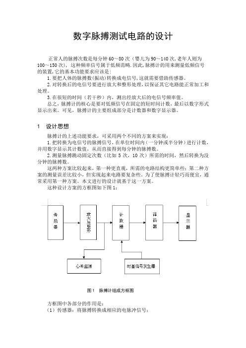
数字脉搏测试电路的设计正常人的脉搏次数是每分钟60~80次(婴儿为90~140次,老年人则为100~150次), 这种频率信号属于低频范畴.因此,脉搏计的用来测量低频信号的装置,它的基本功能要求应该是:1.要把人体的脉搏数(振动)转换成电信号,这就需要借助传感器。
2.对转换后的电信号要进行放大和整形处理,以保证其它电路能正常加工和处理。
3.在很短的时间(若干秒)内,测出经放大后的电信号频率值。
总之,脉搏计的核心是要对低频信号在固定的短时间计数,最后以数字形式显示出来。
可见,脉搏计的主要组成部分是计数器和数字显示器。
1 设计思想脉搏计的上述功能要求,可采用两个不同的方案来实现:1.把转换为电信号的脉搏信号,在单位时间内(一分钟或半分钟)进行计数,并用数字显示其计数值,从而直接得到每分钟的脉搏数。
2.测量脉搏跳动固定次数(比如5次,10次)所需的时间,然后转换为没分钟的脉搏数。
这两种方案比较起来,第一种更直观,所需的电路结构更简单些;第二种方案的测量误差比较小,但实现起来电路要复杂些。
为了使脉搏计轻巧而便宜,通常采用第一种方案。
本文进行的设计就基于这一方案。
这种设计方案的方框图如下图1:图1 脉搏计组成方框图方框图中各部分的作用是:(1)传感器:将脉搏转换成相应的电脉冲信号;(2)放大电路:对微小电脉冲信号进行放大;(3)时基产生电路:产生固定时间(1分钟或半分钟)的控制信号,作为计数器的门控,使计数器只有在此期间才进行计数;(4)计数、译码、显示电路:在门控信号作用期间,对电脉冲信号进行技术,并显示译码器译码,再由数码管显示计数值;(5)心率监测电路:如果出现心率不齐,应有所告警。
2 功能模块实现2.1 传感器为了把脉搏转换成电信号,应采用压电式传感器。
它有两种基本类型:石英晶体和压电陶瓷。
前者温度稳定性和机械强度都很高,工作温度范围宽,转换精度也高。
而压电陶瓷是人工制造的压电材料。
优点是压电系数大、灵敏度高、价格便宜,只是温度稳定性和强度不如石英晶体。
2SA系列(PNP型)三极管全参数表

-1.5
-180
-160
120M
60-200
3CA10F
2SA1011S
SANYO
硅PNP三极管,功率放大,场输出,配对管2SC2344
25
-1.5
-180
-160
120M
60-200
3CA10F
2SA1011W
WS
硅PNP三极管,功率放大,场输出,配对管2SC2344
25
-1.5
-180
-160
200m
-500m
-40
-32
200M
82-390
2SA1037AK
ROHM
硅PNP三极管,一般小信号放大,配对管2SC2412K
200m
-150m
-60
-50
140M
120-560
2SA1037B
LRC
硅PNP三极管,一般小信号放大,配对管2SC2412K/2SC4081
200m
-150m
-60
-50
-25
200M
50-340
CK77A
2SA0684
PANASONIC
硅PNP三极管,低频功率放大和驱动,配对管2SC1384
1
-1.5
-60
-50
200M
50-340
CK77A
2SA0794
PANASONIC
硅PNP三极管,低频功率放大和驱动,配对管2SC1567
1.2
-500m
-100
-100
120M
60M
70-240
3CA10D
2SA1013
长电
硅PNP三极管,TO-92,放大
2SC945中文资料(Guangdong Kexin)中文数据手册「EasyDatasheet - 矽搜」
SMD型
NPN硅晶体管 2SC945
■ 特征
● 集电极电流高达150mA
● 高ħ
线性
晶体管二极管
SOT-23
■ 绝对最大额定值大= 25℃
参数 集电极基极电压 集电极到发射极电压 发射器基极电压
集电极电流(DC)
功耗 结温 存储温度范围
■ 电气特性TA = 25℃
参数 集电极基击穿电压
集电极 - 发射极击穿电压
发射基地击穿电压 集电极截止电流 发射极截止电流
DC电流增益
集电极饱和电压 基本饱和电压 收藏家基地电容 噪声系数 转换频率
符
额定值
Unit
V
60
V
V
50
V
V
5
V
I
150
mA
P
200
mW
T
150
℃
T
-55到+150
℃
符
V V V
I I
h
V V
C NF f
Min Typ Max Unit
60
V
50
V
μA
130
400
40
0.3 V
1.0 V
3.0 pF
4 10 dB
150
MHz
1
芯片中文手册,看全文,戳
SMD型
2SC945
晶体管二极管
2
Testconditons I =100 μA, I =0 I =1mA, I =0 I =100 μA, I =0 V = 60V, I = 0 V = 5.0 V, I = 0 V = 6.0V, I =1.0mA V = 6.0V, I =0.1mA I =100mA,I =10mA I =100mA,I =10mA V = 10 V, I = 0,F = 1兆赫 V =6V,I =0.1mA,R =10kΩ,f=1kMHZ V =6V,I =10毫安,F = 30兆赫
2SC3356R25中文资料(NEC)中文数据手册「EasyDatasheet - 矽搜」
–150˚ –120˚
–30˚ –150˚
–60˚ –90˚
–120˚
–30˚
–60˚ –90˚
Data Sheet PU10209EJ02V0DS
5
10
插入最功大率可增5用益功|率SV增益=M1A0GV(分贝)
I 能力= 20 mA
0 0.05 0.1 0.2
0.5
1
2
频率f(GHz)
5 插入功率增益| S
0
0.5 1
5
集电极电流I
10 (mA)
50 70
备注
该图表显示标称特性.
Data Sheet PU10209EJ02V0DS
3
芯片中文手册,看全文,戳
2%
2. 收藏家基地电容,当发射器接地
hFE 分类
秩 打标
h值
R23/Q R23
50至100
R24/R R24
80至160
R25/S R25
125至250
注意 旧规格/新规格
MIN.
TYP. MAX.
单元
–
–
1.0
µA
–
–
1.0
µA
50
120
250
–
–
7
–
GHz
–
11.5
–
dB
–
1.1
2.0
dB0.55订源自信息零件号2SC3356 2SC3356-T1B
数量
50只(不卷) 3千件/卷
供给方式
•8mm宽压花录音 •引脚3(集电极)面带穿孔方
备注
要订购评价样品,请联系您最近销售部门. 单位样品数量为50个.
绝对最大额定值(T
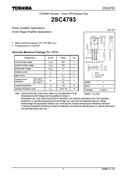
2SC4793中文资料
TOSHIBA Transistor Silicon NPN Epitaxial Type2SC4793Power Amplifier ApplicationsDriver Stage Amplifier Applications• High transition frequency: f T = 100 MHz (typ.) • Complementary to 2SA1837Absolute Maximum Ratings (Tc = 25°C)Characteristics Symbol Rating UnitCollector-base voltage V CBO 230 V Collector-emitter voltage V CEO 230 V Emitter-base voltage V EBO 5 V Collector current I C 1 A Base current I B 0.1 A Ta = 25°C 2.0 Collector powerdissipationTc = 25°CP C20WJunction temperature T j 150 °C Storage temperature rangeT stg−55 to 150°CNote: Using continuously under heavy loads (e.g. the application of high temperature/current/voltage and the significant change intemperature, etc.) may cause this product to decrease in the reliability significantly even if the operating conditions (i.e. operating temperature/current/voltage, etc.) are within the absolute maximum ratings. Please design the appropriate reliability upon reviewing the Toshiba Semiconductor Reliability Handbook(“Handling Precautions”/Derating Concept and Methods) and individual reliability data (i.e. reliability test report and estimated failure rate, etc).Unit: mmJEDEC― JEITA ―TOSHIBA 2-10R1AWeight: 1.7 g (typ.)Electrical Characteristics (Tc = 25°C)Typ.Max UnitCondition Min Characteristics Symbol TestCollector cut-off current I CBO V CB = 230 V, I E = 0 ―― 1.0 μA Emitter cut-off current I EBO V EB = 5 V, I C = 0 ―― 1.0 μA Collector-emitter breakdown voltage V (BR) CEO I C = 10 mA, I B = 0 230 ―― V DC current gain h FE V CE = 5 V, I C = 100 mA 100 ― 320Collector-emitter saturation voltage V CE (sat)I C = 500 mA, I B = 50 mA ―― 1.5 V Base-emitter voltage V BE V CE = 5 V, I C = 500 mA ―― 1.0 V Transition frequency f T V CE = 10 V, I C = 100 mA ― 100 ― MHz Collector output capacitance C ob V CB = 10 V, I E = 0, f = 1 MHz ― 20 ― pF MarkingC4793lead (Pb)-free package orlead (Pb)-free finish.Collector-emitter voltage V CE (V) I C – V CEC ol le c t o r c u r r e n tI C (A )Base-emitter voltage V BE (V)I C – V BEC o l l ec t o r c u r r e n t I C(A )Collector current I C (A)V CE (sat) – I CD C c u r r e n t g a i nh F ECollector current I C (A)V CE (sat) – I CC o l l e c t o r -e m i t t e r s a t u r a t io n vo l t a g e V C E (s a t )(V )Collector current I C (mA) f T – I CT r a n s it i on f r e q u e n c yf T (M H z )Collector-emitter voltage V CE (V)Safe Operating AreaC o l l e c t o r c u r r e n t I C (A )131030 100 300RESTRICTIONS ON PRODUCT USE20070701-EN •The information contained herein is subject to change without notice.•TOSHIBA is continually working to improve the quality and reliability of its products. Nevertheless, semiconductor devices in general can malfunction or fail due to their inherent electrical sensitivity and vulnerability to physical stress. It is the responsibility of the buyer, when utilizing TOSHIBA products, to comply with the standards of safety in making a safe design for the entire system, and to avoid situations in which a malfunction or failure of such TOSHIBA products could cause loss of human life, bodily injury or damage to property.In developing your designs, please ensure that TOSHIBA products are used within specified operating ranges as set forth in the most recent TOSHIBA products specifications. Also, please keep in mind the precautions and conditions set forth in the “Handling Guide for Semiconductor Devices,” or “TOSHIBA Semiconductor Reliability Handbook” etc.• The TOSHIBA products listed in this document are intended for usage in general electronics applications (computer, personal equipment, office equipment, measuring equipment, industrial robotics, domestic appliances, etc.).These TOSHIBA products are neither intended nor warranted for usage in equipment that requires extraordinarily high quality and/or reliability or a malfunction or failure of which may cause loss of human life or bodily injury (“Unintended Usage”). Unintended Usage include atomic energy control instruments, airplane or spaceship instruments, transportation instruments, traffic signal instruments, combustion control instruments, medical instruments, all types of safety devices, etc.. Unintended Usage of TOSHIBA products listed in his document shall be made at the customer’s own risk.•The products described in this document shall not be used or embedded to any downstream products of which manufacture, use and/or sale are prohibited under any applicable laws and regulations.• The information contained herein is presented only as a guide for the applications of our products. No responsibility is assumed by TOSHIBA for any infringements of patents or other rights of the third parties which may result from its use. No license is granted by implication or otherwise under any patents or other rights of TOSHIBA or the third parties.• Please contact your sales representative for product-by-product details in this document regarding RoHS compatibility. Please use these products in this document in compliance with all applicable laws and regulations that regulate the inclusion or use of controlled substances. Toshiba assumes no liability for damage or losses occurring as a result of noncompliance with applicable laws and regulations.。
2SC5103TLQ中文资料
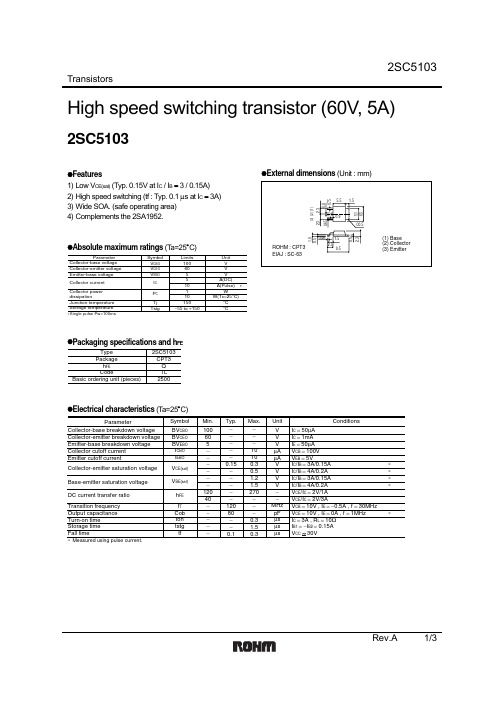
TransistorsRev.A 1/3High speed switching transistor (60V, 5A)2SC5103z Features1) Low V CE(sat) (Typ. 0.15V at I C / I B = 3 / 0.15A) 2) High speed switching (tf : Typ. 0.1 µs at I C = 3A) 3) Wide SOA. (safe operating area) 4) Complements the 2SA1952.z Absolute maximum ratings (T a=25°C)ParameterSymbol V CBO V CEO V EBOI C P C Tj Tstg Limits 10060551150−55 to +150Unit V V V A(DC)10∗A(Pulse)W10W(Tc =25°C)°C °CSingle pulse Pw=100msCollector-base voltage Collector-emitter voltage Emitter-base voltage Collector current Junction temperature Storage temperatureCollector power dissipation∗z Packaging specifications and h FEType 2SC5103CPT3Q TL 2500Package h FE CodeBasic ordering unit (pieces)z External dimensions (Unit : mm)2.30.51.00.59.52.50.8Min.1.56.52.3(2)(3)C0.50.650.9(1)0.752.30.91.55.5(3) Emitter(2) Collector (1) Base ROHM : CPT3EIAJ : SC-635.1z Electrical characteristics (T a=25°C)TransistorsRev.A 2/3zElectrical characteristics curvesC O L L E C T O R C U R R E N T : I C (A )COLLECTOR TO EMITTER VOLTAGE : V CE (V)Fig.1 Ground emitter output characteristicsBASE TO EMITTER VOLTAGE : V BE (V)C O L L E C T O R C U R R E N T : I C (A )Fig.2 Ground emitter propagation characteristicsD C C U R RE N T G A I N : hF ECOLLECTOR CURRENT : I C (A)Fig.3 DC current gain vs. collector currentB A S E S A T U R A T I O N V O L T A G E : V B E (s a t ) (V )C O L L E C T O R S A T U R A T I O N V O L T A G E: V C E (s a t ) (V )COLLECTOR CURRENT : I C (A )Fig.4 Collector-emitter saturation voltageBase-emitter saturation voltage −collector currentC O L L E C T O R O U T P U T C A P A C I T W A N C E : C o b (p F )COLLECTOR TO BASE VOLTAGE : V CB (V)Fig.6 Collector output capacitance vs. collector-base voltage−T R A N S I T I O N F R E Q U E N C Y : f T (M H z )EMITTER CURRENT : I E (A)Fig.5 Gain bandwidth product vs.emitter currentS T R A G E T I M E : t s t g (µs )F A L LT I M E : t f (µs )T U R N O N T I M E : t o n (µs )COLLECTOR CURRENT : I C (A)Fig.7 Switching characteristicsCOLLECTOR TO EMITTER VOLTAGE : V CE (V)C O L L E C T O R C U R R E N T : I C (A )Fig.8 Safe operating areaTIME : t (s)T R A N S I E N T T H E R M A L R E S I S T A N C E : R t h (°C /W )Fig.9 Transient thermal resistanceTransistorsRev.A 3/3BBFig.10 Switching characteristic circuitAppendixAbout Export Control Order in JapanProducts described herein are the objects of controlled goods in Annex 1 (Item 16) of Export T rade ControlOrder in Japan.In case of export from Japan, please confirm if it applies to "objective" criteria or an "informed" (by MITI clause)on the basis of "catch all controls for Non-Proliferation of Weapons of Mass Destruction.Appendix1-Rev1.1。
2SC2655中文资料(secos)中文数据手册「EasyDatasheet - 矽搜」

Min. Typ. Max.
50
-
-
50
-
-
5
-
-
-
-
1
-
-
1
70
-
240
40
-
-
-
-
0.5
-
-
1.2
-
100
-
-
30
-
-
0.15
-
-
2
-
-
0.15
-
单元 V V V μA μA
V V MHz pF
μs
测试条件
IC=100μA, I E=0 IC=10mA, I B=0 IE=100μA, I C=0 VCB=50V, I E=0 VEB=5V, I C=0 VCE=2V, I C=0.5A VCE=2V, I C=1.5A IC=1A, I B=0.05A IC=1A, I B=0.05A VCE=2V, I C=0.5A VCB=10V, I E=0, f=1MHz VCC=30V IB1= -I B2=0.05A IC=1A
芯片中文手册,看全文,戳
2SC2655
2A , 50V NPN塑料封装晶体管
符合RoHS产品 "-C"后缀指定卤素及无铅
特征
低饱和电压:V 高速切换时间:T已 为补充2SA1020
CE(sat) =0.5V(Max)(I C=1A) stg=1μs(Typ.)
^ h分类
产品秩 范围
FE (1) 2SC2655-O
70-140
2SC2655-Y 120-240
收藏家
基地
发射器
TO-92MOD
A
- 1、下载文档前请自行甄别文档内容的完整性,平台不提供额外的编辑、内容补充、找答案等附加服务。
- 2、"仅部分预览"的文档,不可在线预览部分如存在完整性等问题,可反馈申请退款(可完整预览的文档不适用该条件!)。
- 3、如文档侵犯您的权益,请联系客服反馈,我们会尽快为您处理(人工客服工作时间:9:00-18:30)。
The information in this document is subject to change without notice. Before using this document, please confirm that this is the latest version.Not all devices/types available in every country. Please check with local NEC representative for availability and additional information.1998©Document No. D15599EJ2V0DS00 (2nd edition)Date Published April 2002 N CP(K)Printed in JapanSILICON POWER TRANSISTOR2SC4553NPN SILICON EPITAXIAL TRANSISTORFOR HIGH-SPEED SWITCHINGDATA SHEET2002The 2SC4553 is a power transistor designed especially for low collector saturation voltage and features large current switching at a low power dissipation. In addition, a high h FE enables alleviation of the driver load.FEATURES•High h FE and low V CE(sat):h FE ≅ 800 (V CE = 2 V, I C = 3 A)V CE(sat) ≅ 0.12 V (I C = 3 A, I B = 0.03 A)•On-chip C to E damper diode•Mold package that does not require an insulating board or insulation bushingABSOLUTE MAXIMUM RATINGS (Ta = 25°C)ParameterSymbol Ratings Unit Collector to base voltage V CBO 100V Collector to emitter voltage V CEO 100V Emitter to base voltage V EBO 7.0V Collector current (DC)I C(DC)±7.5A Collector current (pulse)I C(pulse)*±10A Base current (DC)I B(DC)2.0A Total power dissipation P T (Tc = 25°C)30W Total power dissipation P T (Ta = 25°C)2.0W Junction temperature T j 150°C Storage temperatureT stg−55 to +150°C*PW ≤ 10 ms, duty cycle ≤ 50%PACKAGE DRAWING (UNIT: mm)(OHFWURGH &RQQHFWLRQ %DVH &ROOHFWRU (PLWWHU(48,9$/(17 &,5&8,7Data Sheet D15599EJ2V0DS2ELECTRICAL CHARACTERISTICS (Ta = 25°C)3DUDPHWHU6\PERO &RQGLWLRQV0,17<30$; 8QLW&ROOHFWRU FXWRII FXUUHQW ,&%29&% 9 ,( µ$(PLWWHU FXWRII FXUUHQW ,(%29(% 9 ,& P$'& FXUUHQW JDLQ K )( 9&( 9 ,& $'& FXUUHQW JDLQK )( 9&( 9 ,& $&ROOHFWRU VDWXUDWLRQ YROWDJH 9&( VDW ,& $ ,% P$ 9&ROOHFWRU VDWXUDWLRQ YROWDJH 9&( VDW ,& $ ,% P$9&ROOHFWRU VDWXUDWLRQ YROWDJH 9&( VDW ,& $ ,% P$ 9&ROOHFWRU VDWXUDWLRQ YROWDJH 9&( VDW ,& $ ,% P$ 9%DVH VDWXUDWLRQ YROWDJH 9%( VDW,& $ ,% P$9*DLQ EDQGZLGWK SURGXFW I 79&( 9 ,& $ 0+]&ROOHFWRU FDSDFLWDQFH &RE 9&% 9 ,( I 0+] S)7XUQ RQ WLPH W RQ µV 6WRUDJH WLPH W VWJ µV )DOO WLPHW I ,& $ 5/ Ω,% −,% P$ 9&& ≅ 95HIHU WR WKH WHVW FLUFXLW µV 'LRGH IRUZDUG YROWDJH9'),') $9SWITCHING TIME (t RQ , t VWJ , t I ) TEST CIRCUIT%DVH FXUUHQW ZDYHIRUP&ROOHFWRU FXUUHQW ZDYHIRUPData Sheet D15599EJ2V0DS3TYPICAL CHARACTERISTICS (Ta = 25°C)7R W D O 3R Z H U 'L V V L S D W L R Q 37 :&DVH 7HPSHUDWXUH 7& °&&R O O H F W R U &X U U H Q W ,& $&ROOHFWRU WR (PLWWHU 9ROWDJH 9&( 9,& 'H U D W L Q J G 7&DVH 7HPSHUDWXUH 7& °&6LQJOH SXOVH7U D Q V L H Q W 7K H U P D O 5H V L V W D Q F H 5W K M −F °& :3XOVH :LGWK 3: V:LWKRXW KHDWVLQN:LWK LQILQLWH KHDWVLQNData Sheet D15599EJ2V0DS4&ROOHFWRU &XUUHQW ,& $&ROOHFWRU &XUUHQW ,& $&R O O H F W R U 6D W X U D W L R Q 9R O W D J H 9&( V D W 9%D V H 6D W X U D W L R Q 9R O W D J H 9%( V D W 9&R O O H F W R U &X U U H Q W ,& $&ROOHFWRU WR (PLWWHU 9ROWDJH 9&( 9&ROOHFWRU &XUUHQW ,& $'& &X U U H Q W *D L Q K )([MEMO]Data Sheet D15599EJ2V0DS5M8E 00. 4The information in this document is current as of July, 2001. The information is subject to change without notice. For actual design-in, refer to the latest publications of NEC's data sheets or data books, etc., for the most up-to-date specifications of NEC semiconductor products. Not all products and/or types are available in every country. Please check with an NEC sales representative for availability and additional information.No part of this docume nt may be copie d or re produce d in any form or by any me ans without prior written consent of NEC. NEC assumes no responsibility for any errors that may appear in this document.NEC does not assume any liability for infringement of patents, copyrights or other intellectual property rights of third parties by or arising from the use of NEC semiconductor products listed in this document or any other liability arising from the use of such products. No license, express, implied or otherwise, is granted under any patents, copyrights or other intellectual property rights of NEC or others.Descriptions of circuits, software and other related information in this document are provided for illustrative purpose s in se miconductor product ope ration and application e xample s. The incorporation of the se circuits, software and information in the de sign of custome r's e quipme nt shall be done unde r the full re sponsibility of customer. NEC assume s no re sponsibility for any losse s incurre d by custome rs or third parties arising from the use of these circuits, software and information.While NEC endeavours to enhance the quality, reliability and safety of NEC semiconductor products, customers agre e and acknowle dge that the possibility of de fe cts the re of cannot be e liminate d e ntire ly. To minimize risks of damage to prope rty or injury (including de ath) to pe rsons arising from de fe cts in NEC se miconductor products, custome rs must incorporate sufficie nt safe ty me asure s in the ir de sign, such as redundancy, fire-containment, and anti-failure features.NEC semiconductor products are classified into the following three quality grades:"Standard", "Spe cial" and "Spe cific". The "Spe cific" quality grade applie s only to se miconductor products de ve lope d base d on a custome r-de signate d "quality assurance program" for a spe cific application. The re comme nde d applications of a se miconductor product de pe nd on its quality grade , as indicate d be low. Custome rs must che ck the quality grade of e ach se miconductor product be fore using it in a particular application."Standard":Computers, office equipment, communications equipment, test and measurement equipment, audioand visual equipment, home electronic appliances, machine tools, personal electronic equipment and industrial robots"Special":Transportation equipment (automobiles, trains, ships, etc.), traffic control systems, anti-disastersystems, anti-crime systems, safety equipment and medical equipment (not specifically designed for life support)"Specific":Aircraft, aerospace equipment, submersible repeaters, nuclear reactor control systems, lifesupport systems and medical equipment for life support, etc.The quality grade of NEC semiconductor products is "Standard" unless otherwise expressly specified in NEC's data she e ts or data books, e tc. If custome rs wish to use NEC se miconductor products in applications not intended by NEC, they must contact an NEC sales representative in advance to determine NEC's willingness to support a given application.(Note)(1)"NEC" as used in this statement means NEC Corporation and also includes its majority-owned subsidiaries.(2)"NEC semiconductor products" means any semiconductor product developed or manufactured by or forNEC (as defined above).••••••。