ADS8342IPFBT;ADS8342IBPFBT;ADS8342IPFBTG4;ADS8342IBPFBTG4;ADS8342IBPFBR;中文规格书,Datasheet资料
[计算机硬件及网络]AolynkDR834ADSL2安全路由器用户手册
![[计算机硬件及网络]AolynkDR834ADSL2安全路由器用户手册](https://img.taocdn.com/s3/m/5f379a57964bcf84b9d57bcc.png)
Aolynk DR834 ADSL2 安全路由器用户手册目录1 产品简介1.1 概述1.2 外观1.2.1 前面板1.2.2 后面板1.3 产品特性2 安装2.1 装箱清单2.2 安装注意事项2.3 连接线缆3 Web配置入门3.1 配置准备3.2 登录3.3 页面相关介绍3.4 路由器缺省设置4 Web基础配置4.1 快速设置(Quick Setup)4.2 广域网设置(WAN Setup)4.2.1 WAN业务配置4.2.2 DNS中继4.2.3 DDNS4.2.4 PVC 搜索4.3 局域网设置(LAN Setup)4.3.1 LAN4.3.2 DHCP4.3.3 DHCP客户端4.4 设备(Device)4.4.1 重启/恢复出厂设置(Restart) 4.4.2 密码(Password)4.4.3 远程访问(Remote)4.4.4 备份/恢复配置(Backup)4.4.5 升级(Upgrade)4.5 状态(Status)4.5.1 状态记录4.5.2 数据传输通道(Channels)4.5.3 端口状态(Ports)4.5.4 日志(Log)4.5.5 Ping4.6 保存配置(Save Config)5 高级配置5.1 安全(Security)5.1.1 虚拟服务器(Virtual Server) 5.1.2 防火墙(Firewall)5.1.3 触发器(Trigger)5.1.4 NAT5.1.5 IDS5.2 路由配置(Route)5.2.1 静态路由配置5.2.2 动态路由配置5.3 服务(Service)5.3.1 SNTP5.3.2 SNMP5.3.3 IGMP代理5.4 VPN设置5.4.1 IPSec安全配置5.4.2 密钥管理配置5.4.3 VPN设置举例6 典型配置案例6.1 企业典型需求6.2 组网配置方案6.3 组网图6.4 配置步骤6.5 VPN接入设备的有关配置7 故障排除7.1 故障排除建议7.2 诊断工具7.2.1 Ping7.2.2 Nslookup8 常见问题解答(FAQ)9 附录 - 安装与配置TCP/IP协议9.1 安装TCP/IP协议9.2 配置TCP/IP协议9.2.1 自动获取IP地址9.2.2 指定静态IP地址10 附录 - 配置连接USB接口的PC 10.1 安装USB驱动10.2 配置连接USB接口的PC的IP属性11 附录 - IP地址相关知识简介11.1 IP地址11.1.1 IP地址的结构11.1.2 网络地址分类11.2 子网掩码12 附录 - 技术规格13 附录 - 术语1 产品简介本章简要介绍了Aolynk DR834 ADSL2+安全路由器的外观与功能特性,让用户快速熟悉本产品。
MuxLab 3G-SDI ST2110 over IP 无压缩网关转换器快速安装指南说明书
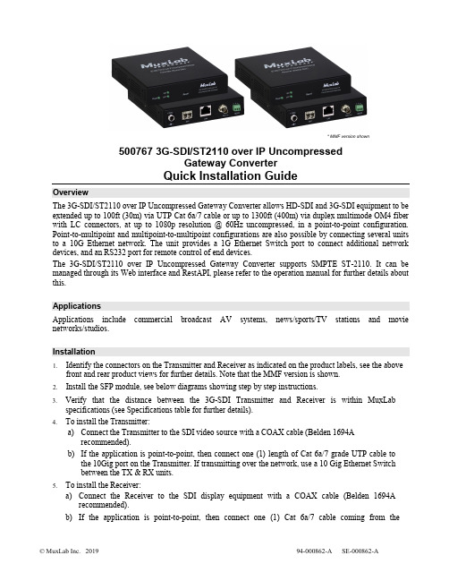
* MMF version shown500767 3G-SDI/ST2110 over IP UncompressedGateway ConverterQuick Installation GuideOverviewThe 3G-SDI/ST2110 over IP Uncompressed Gateway Converter allows HD-SDI and 3G-SDI equipment to be extended up to 100ft (30m) via UTP Cat 6a/7 cable or up to 1300ft (400m) via duplex multimode OM4 fiber with LC connectors, at up to 1080p resolution @ 60Hz uncompressed, in a point-to-point configuration. Point-to-multipoint and multipoint-to-multipoint configurations are also possible by connecting several units to a 10G Ethernet network. The unit provides a 1G Ethernet Switch port to connect additional network devices, and an RS232 port for remote control of end devices.The 3G-SDI/ST2110 over IP Uncompressed Gateway Converter supports SMPTE ST-2110. It can be managed through its Web interface and RestAPI, please refer to the operation manual for further details about this.ApplicationsApplications include commercial broadcast AV systems, news/sports/TV stations and movie networks/studios.Installation1.Identify the connectors on the Transmitter and Receiver as indicated on the product labels, see the abovefront and rear product views for further details. Note that the MMF version is shown.2.Install the SFP module, see below diagrams showing step by step instructions.3.Verify that the distance between the 3G-SDI Transmitter and Receiver is within MuxLabspecifications (see Specifications table for further details).4.To install the Transmitter:a)Connect the Transmitter to the SDI video source with a COAX cable (Belden 1694Arecommended).b)If the application is point-to-point, then connect one (1) length of Cat 6a/7 grade UTP cable tothe 10Gig port on the Transmitter. If transmitting over the network, use a 10 Gig Ethernet Switchbetween the TX & RX units.5.To install the Receiver:a)Connect the Receiver to the SDI display equipment with a COAX cable (Belden 1694Arecommended).b)If the application is point-to-point, then connect one (1) Cat 6a/7 cable coming from theTransmitter, to the 10Gig port on the Receiver. If transmitting over the network, use a 10Gig Ethernet Switch between the TX & RX units.6.If the configuration is a point-to-multipoint or multipoint-to-multipoint:a)You will need to use an Ethernet Switch with Gigabit ports and DHCP Server support. In additionIGMP Protocol support is required for the multipoint-to-multipoint case. Verify that the Ethernet Switch is configured correctly and that the DHCP Server is enabled and that the IGMP Protocol is enabled for multipoint-to-multipoint applications.b)Connect all Transmitters and Receivers to the Ethernet Switch.7.Connect the 12 VDC power supply to each Receiver and to an AC power outlet. Next connect eachTransmitter in the same manner. If power is present, the green power LED on each Transmitter and Receiver will illuminate.Note: Power ‘ON’ the 3G-SDI / ST2110 over IP uncompressed gateway converter only after all data connections have been made.8.Power ‘ON’ the 3G-SDI equipment and verify the image quality.9.The 500767 provides a 1GB Ethernet port to connect additional network devices (e.g. RestAPI controlsoftware).10.This product supports RS232 for remote control on end devices.11.The following diagram illustrates a typical point-to-multipoint LAN configuration.TroubleshootingThe following table describes some of the symptoms, probable causes and possible solutions in regard to the installation of the 3G-SDI/ST2110 over IP Uncompressed Gateway:If you still cannot diagnose the problem, please call MuxLab Customer Technical Support at 877-689-5228 (toll-free in North America) or (+1) 514-905-0588 (International).SFP Module Installation2321 Cohen Street, Montreal, Quebec, Canada. H4R 2N7Tel: (514) 905-0588 Fax: (514) 905-0589 Toll Free (North America): (877) 689-5228E-mail:******************:。
AD8342资料
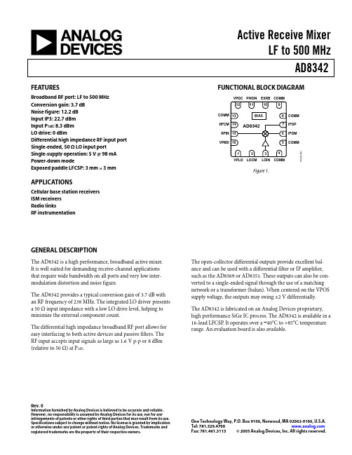
Active Receive MixerLF to 500 MHzAD8342 Rev.0Information furnished by Analog Devices is believed to be accurate and reliable.However, no responsibility is assumed by Analog Devices for its use, nor for anyinfringements of patents or other rights of third parties that may result from its use. Specifications subject to change without notice. No license is granted by implication or otherwise under any patent or patent rights of Analog Devices. Trademarks and registered trademarks are the property of their respective owners.One Technology Way, P.O. Box 9106, Norwood, MA 02062-9106, U.S.A. Tel: Fax: 781.461.3113© 2005 Analog Devices, Inc. All rights reserved.FEATURESBroadband RF port: LF to 500 MHz Conversion gain: 3.7 dBNoise figure: 12.2 dBInput IP3: 22.7 dBmInput P1dB: 8.3 dBmLO drive: 0 dBmDifferential high impedance RF input port Single-ended, 50 Ω LO input portSingle-supply operation: 5 V @ 98 mA Power-down modeExposed paddle LFCSP: 3 mm × 3 mmAPPLICATIONSCellular base station receiversISM receiversRadio linksRF instrumentation FUNCTIONAL BLOCK DIAGRAMCOMMIFOPIFOMCOMM COMMRFCMRFINVPMXVPDC PWDN EXRB COMMVPLO LOCM LOIN COMM05352-1Figure 1.GENERAL DESCRIPTIONThe AD8342 is a high performance, broadband active mixer.It is well suited for demanding receive-channel applications that require wide bandwidth on all ports and very low inter-modulation distortion and noise figure.The AD8342 provides a typical conversion gain of 3.7 dB with an RF frequency of 238 MHz. The integrated LO driver presents a 50 Ω input impedance with a low LO drive level, helping to minimize the external component count.The differential high impedance broadband RF port allows for easy interfacing to both active devices and passive filters. The RF input accepts input signals as large as 1.6 V p-p or 8 dBm (relative to 50 Ω) at P1dB. The open-collector differential outputs provide excellent bal-ance and can be used with a differential filter or IF amplifier, such as the AD8369 or AD8351. These outputs can also be con-verted to a single-ended signal through the use of a matching network or a transformer (balun). When centered on the VPOS supply voltage, the outputs may swing ±2 V differentially.The AD8342 is fabricated on an Analog Devices proprietary, high performance SiGe IC process. The AD8342 is available in a 16-lead LFCSP. It operates over a −40°C to +85°C temperature range. An evaluation board is also available.AD8342Rev. 0 | Page 2 of 20TABLE OF CONTENTSSpecifications.....................................................................................3 AC Performance...............................................................................4 Spur Table..........................................................................................5 Absolute Maximum Ratings............................................................6 ESD Caution..................................................................................6 Pin Configuration and Function Descriptions.............................7 Typical Performance Characteristics.............................................8 Circuit Description.........................................................................14 AC Interfaces...................................................................................15 IF Port..........................................................................................16 LO Considerations.....................................................................17 High IF Applications..................................................................18 Evaluation Board............................................................................19 Outline Dimensions.......................................................................20 Ordering Guide.. (20)REVISION HISTORY4/05—Revision 0: Initial VersionAD8342Rev. 0 | Page 3 of 20SPECIFICATIONSV S = 5 V , T A = 25°C, f RF = 238 MHz, f LO = 286 MHz, LO power = 0 dBm, Z O = 50 Ω, R BIAS = 1.82 kΩ, RF termination = 100 Ω, IF termi-nated into 100 Ω through a 2:1 ratio balun, unless otherwise noted. Table 1.ParameterConditions Min Typ Max Unit RF INPUT INTERFACEReturn LossHi-Z input terminated with 100 Ω off-chip resistor10 dB Input Impedance Frequency = 238 MHz (measured at RFIN with RFCM ac-grounded)1||0.4 kΩ||pF DC Bias Level Internally generated; port must be ac-coupled 2.4 V OUTPUT INTERFACEOutput Impedance Differential impedance, frequency = 48 MHz 10||0.5 kΩ||pF DC Bias Voltage Supplied externally4.75 V S5.25 V Power Range Via a 2:1 impedance ratio transformer 13 dBm LO INTERFACE Return Loss10dB DC Bias VoltageInternally generated; port must be ac-coupled V S − 1.6 V POWER-DOWN INTERFACE PWDN Threshold3.5 V PWDN Response Time Device enabled, IF output to 90% of its final level 0.4 µsDevice disabled, supply current <5 mA 4 µs PWDN Input Bias Current Device enabled −80 µADevice disabled +100 µA POWER SUPPLYPositive Supply Voltage 4.75 5 5.25 V Quiescent CurrentVPDCSupply current for bias cells5 mA VPMX, IFOP, IFOM Supply current for mixer, R BIAS = 1.82 kΩ 58 mA VPLOSupply current for LO limiting amplifier 35 mA Total Quiescent Current V S = 5 V85 98 113 mA Power-Down CurrentDevice disabled500µAAD8342Rev. 0 | Page 4 of 20AC PERFORMANCEV S = 5 V , T A = 25°C, LO power = 0 dBm, Z O = 50 Ω, R BIAS = 1.82 kΩ, RF termination 100 Ω, IF terminated into 100 Ω via a 2:1 ratio balun, unless otherwise noted. Table 2.ParameterConditions MinTyp Max Unit RF FREQUENCY RANGE 150 500 MHz LO FREQUENCY RANGE 1 High side LO 60 850 MHz IF FREQUENCY RANGE 110 350 MHz CONVERSION GAIN f RF = 460 MHz, f LO = 550 MHz, f IF = 90 MHz 3.2 dBf RF = 238 MHz, f LO = 286 MHz, f IF = 48 MHz 3.7 dB SSB NOISE FIGURE f RF = 460 MHz, f LO = 550 MHz, f IF = 90 MHz 12.5 dBf RF = 238 MHz, f LO = 286 MHz, f IF = 48 MHz 12.2 dB INPUT THIRD-ORDER INTERCEPTf RF1 = 460 MHz, f RF2 = 461 MHz, f LO = 550 MHz, f IF1 = 90 MHz, f IF2 = 89 MHz each RF tone −10 dBm22.2 dBmf RF1 = 238 MHz, f RF2 = 239 MHz, f LO = 286MHz,f IF1 = 48MHz, f IF2 = 47MHz each RF tone −10 dBm22.7 dBm INPUT SECOND-ORDER INTERCEPT f RF1 = 460 MHz, f RF2 = 410 MHz, f LO = 550 MHz, f IF1 = 90 MHz,f IF2 = 140 MHz50 dBm f RF1 = 238 MHz, f RF2 = 188 MHz, f LO = 286 MHz, f IF1 = 48MHz,f IF2 = 98 MHz44 dBm INPUT 1 dB COMPRESSION POINT f RF = 460 MHz, f LO = 550 MHz, f IF = 90 MHz 8.5 dBm f RF = 238 MHz, f LO = 286 MHz, f IF = 48 MHz 8.3 dBm LO TO IF OUTPUT LEAKAGE LO power = 0 dBm, f LO = 286 MHz −27 dBc LO TO RF INPUT LEAKAGE LO power = 0 dBm, f LO = 286 MHz −55 dBc2× LO TO IF OUTPUT LEAKAGE LO power = 0 dBm, f RF = 238 MHz, f LO = 286 MHzIF terminated into 100 Ω and measured with a differential probe−47 dBm RF TO IF OUTPUT LEAKAGE RF power = −10 dBm, f RF = 238 MHz, f LO = 286 MHz −32 dBc IF/2 SPURIOUS RF power = −10 dBm, f RF = 238 MHz, f LO = 286 MHz−70dBc1Frequency ranges are those that were extensively characterized; this device can operate over a wider range. See the H section for details.igh IF ApplicationsAD8342Rev. 0 | Page 5 of 20SPUR TABLEV S = 5 V , T A = 25°C, RF and LO power = 0 dBm, f RF = 238MHz, f LO = 286MHz, Z O = 50 Ω, R BIAS = 1.82 kΩ, RF termination 100 Ω, IF terminated into 100 Ω via a 2:1 ratio balun.Note: Measured using standard test board. Typical noise floor of measurement system = −100 dBm. Table 3.mnf RF − mf LO0 1 2 3 4 5 6 7 8 9 10 11 12 13 140 <−100 −25 −54 −28 −45 −35 −39 −36 −42 −57 −44 −42 −41 −46 −591 −39 3.5 −42 −6 −48 −16 −50 −28 −57 −37 −68 −45 −54 −37 −61 2 −52 −47 −51 −49 −54 −56 −56 −62 −62 −66 −71 −80 −80 −67 −793 −81 −57 −79 −61 −82 −61 −74 −69 −94 −85 −89 −86 −86 −90 −81 4 −78 −70 −80 −79 −80 −85 −87 −92 −93 −96 −95 <−100 −97 <−100 −95 5 −98 −79 −95 −87 −96 −94 −95 −88 −98 −94 <−100 <−100 <−100 <−100 <−100 6 <−100 <−100 <−100 −99 <−100 −96 <−100 <−100 <−100 <−100 <−100 <−100 <−100 <−100 <−100 7 <−100 <−100 <−100 <−100 −96 <−100 −98 <−100 <−100 <−100 <−100 <−100 <−100 <−100 <−100 8 <−100 <−100 <−100 <−100 <−100 <−100 <−100 <−100 −97 <−100 <−100 <−100 <−100 <−100 <−100 9 <−100 <−100 <−100 <−100 <−100 <−100 <−100 <−100 <−100 <−100 <−100 −99 <−100 <−100 <−100 10 <−100 <−100 <−100 <−100 <−100 <−100 <−100 <−100 <−100 <−100 −99 <−100 <−100 <−100 <−100 11 <−100 <−100 <−100 <−100 <−100 <−100 <−100 −96 <−100 −97 <−100 −96 <−100 <−100 <−100 12 <−100 <−100 <−100 <−100 <−100 <−100 <−100 <−100 −99 <−100 −98 <−100 <−100 <−100 <−100 13 <−100 <−100 <−100 <−100 <−100 <−100 <−100 <−100 <−100 −97 <−100 −97 −99 <−100 <−100 14 <−100 <−100 <−100 <−100 <−100 <−100 <−100 <−100 <−100 <−100 −98 −98 <−100 <−100 <−100 n15 <−100 <−100 <−100 <−100 <−100 <−100 <−100 <−100 <−100 <−100 <−100 <−100 <−100 <−100 <−100AD8342Rev. 0 | Page 6 of 20ABSOLUTE MAXIMUM RATINGSTable 4.ParameterRating Supply Voltage, V S 5.5 V RF Input Level 12 dBm LO Input Level 12 dBm PWDN PinV S + 0.5 V IFOP, IFOM Bias Voltage5.5 V Minimum Resistor from EXRB to COMM 1.8 kΩ Internal Power Dissipation 650 mW θJA77°C/W Maximum Junction Temperature 135°COperating Temperature Range −40°C to +85°C Storage Temperature Range−65°C to +150°CStresses above those listed under Absolute Maximum Ratings may cause permanent damage to the device. This is a stress rating only; functional operation of the device at these or any other conditions above those indicated in the operational sec-tion of this specification is not implied. Exposure to absolute maximum rating conditions for extended periods may affect device reliability.ESD CAUTIONESD (electrostatic discharge) sensitive device. Electrostatic charges as high as 4000 V readily accumulate on the human body and test equipment and can discharge without detection. Although this product features proprietary ESD protection circuitry, permanent damage may occur on devices subjected to high energy electrostatic discharges. Therefore, proper ESD precautions are recommended to avoid performancedegradation or loss of functionality.AD8342Rev. 0 | Page 7 of 20PIN CONFIGURATION AND FUNCTION DESCRIPTIONS05352-0021VPLO 2LOCM 3LOIN 4COMM 11PWDN 12VPDC 10EXRB 9COMM5C O M M 6I F O M 7I F O P 8C O M M 15R F I N16V P M X14R F C M13C O M MFigure 2. 16-Lead LFCSPTable 5. Pin Function Descriptions Pin No. Mnemonic Function 1 VPLO Positive Supply Voltage for the LO Buffer: 4.75 V to 5.25 V. 2 LOCM AC Ground for Limiting LO Amplifier. Internally biased to Vs − 1.6 V. AC-couple to ground. 3 LO IN LO Input. Nominal input level 0 dBm. Input level range −10 dBm to +4 dBm (relative to 50 Ω). Internallybiased to Vs − 1.6 V. AC-couple.4, 5, 8, 9, 13 COMM Device Common (DC Ground). 6, 7 IFOM, IFOP Differential IF Outputs (Open Collectors). Each requires dc bias of 5.00 V (nominal). 10 EXRB Mixer Bias Voltage. Connect resistor from EXRB to ground. Typical value of 1.82 kΩ sets mixer current tonominal value. Minimum resistor value from EXRB to ground = 1.8 kΩ. Internally biased to 1.17 V.11 PWDN Connect to Ground for Normal Operation. Connect pin to V S for disable mode. 12 VPDC Positive Supply Voltage for the DC Bias Cell: 4.75 V to 5.25 V. 14 RFCM AC Ground for RF Input. Internally biased to 2.4 V. AC-couple to ground. 15 RFIN RF Input. Internally biased to 2.4 V. Must be ac-coupled. 16 VPMX Positive Supply Voltage for the Mixer: 4.75 V to 5.25 V.AD8342Rev. 0 | Page 8 of 20TYPICAL PERFORMANCE CHARACTERISTICSV S = 5 V , T A = 25°C, RF power = −10 dBm, LO power = 0 dBm, Z O = 50 Ω, R BIAS = 1.82 kΩ, RF termination 100 Ω, IF terminated into 100 Ω via a 2:1 ratio balun, unless otherwise noted.RF FREQUENCY (MHz)G A I N (d B )50550100150200250300350400450500654321Figure 3. Conversion Gain vs. RF Frequency5005352-025LO LEVEL (dBm)G A I N (d B )–15–10–5054321Figure 4. Gain vs. LO Level, RF Frequency = 238 MHz5.0005352-039TEMPERATURE (°C)G A I N (d B )4.54.03.53.02.52.01.51.00.5–2020406080–40Figure 5. Gain vs. Temperature, f RF = 238 MHz, f LO = 286 MHz51IF FREQUENCY (MHz)G A I N (d B)64325010100150200250300350Figure 6. Conversion Gain vs. IF Frequency5.0005352-026VPOS (V)G A I N (d B )4.54.03.53.02.52.01.51.00.54.755.254.854.955.055.15Figure 7. Gain vs. Vpos, f RF = 238 MHz, f LO= 286 MHz5003.403.90CONVERSION GAIN (238MHz)P E R C E N T A G E45403530252015105 3.453.503.553.603.653.703.753.803.85Figure 8. Conversion Gain Distribution, f RF = 238 MHz, f LO = 286 MHzAD8342Rev. 0 | Page 9 of 20271750550RF FREQUENCY (MHz)I N P U T I P 3 (d B m )100150200250300350400450500262524232221201918Figure 9. Input IP3 vs. RF Frequency2717–15505352-027LO LEVEL (dBm)I N P U T I P 3 (d B m )262524232221201918–13–11–9–7–5–3–113Figure 10. Input IP3 vs. LO Level, f RF1 = 238 MHz, f RF2 = 239 MHz271705352-032TEMPERATURE (°C)I N P U T I P 3 (d B m )–2020406080–40262524232221201918Figure 11. Input IP3 vs. Temperature, f RF1 = 238 MHz, f RF2 = 239 MHz,f LO = 286 MHz 10IF FREQUENCY (MHz)I N P U T I P 3 (d B m )35050100150200250300Figure 12. Input IP3 vs. IF Frequency05352-028VPOS (V)I N P U T I P 3 (d B m )27174.755.25262524232221201918 4.804.854.904.955.005.055.105.155.20Figure 13. Input IP3 vs. Vpos, f RF = 238 MHz, f RF2 = 239 MHzLO Frequency = 286 MHz20020.6INPUT IP3 (238MHz)P E R C E N T A G E1816141210864221.021.421.822.222.623.023.423.824.2Figure 14. Input IP3 Distribution, f RF = 238 MHz, f LO = 286 MHzAD8342Rev. 0 | Page 10 of 2013350550RF FREQUENCY (MHz)I N P U T P 1d B (d B m )121110987654100150200250300350400450500Figure 15. Input P1dB vs. RF Frequency10.05.0–15505352-038LO LEVEL (dBm)I N P U T P 1d B (d B m )9.59.08.58.07.57.06.56.05.5–13–11–9–7–5–3–113Figure 16. Input P1dB vs. LO Level, f RF = 238 MHz10005352-033TEMPERATURE (°C)I N P U T P 1d B (d B m )987654321–2020406080–40Figure 17. Input P1dB vs. Temperature, f RF = 238 MHz, f LO = 286 MHz10010IF FREQUENCY (MHz)I N P U T P 1d B (d B m )98765432150100150200250300350Figure 18. Input P1dB vs. IF Frequency05352-031I N P U T P 1d B (d B m )100987654321VPOS (V)4.755.254.854.955.055.15Figure 19. Input P1dB vs. Vpos, f RF = 238 MHz,f LO= 286 MHz2808.00IP1dB (238MHz)P E R C E N T A G E8.6026242220181614121086428.058.108.158.208.258.308.358.408.458.508.55Figure 20. Input IP3 Distribution, f RF = 238 MHz, f LO = 286 MHzAD8342100550RF FREQUENCY (MHz)I N P U T I P 2 (d B m )150200250300350400450500Figure 21. Input IP2 vs. RF Frequency (Second RF = R F - 50 MHz)604005352-029I N P U T I P 2 (d B m )585654525048464442–155LO LEVEL (dBm)–13–11–9–7–5–3–113Figure 22. Input IP2 vs. LO Level, f RF = 238 MHz, ,f RF2 =188MHz14.011.05055005352-016RF FREQUENCY (MHz)N O I S E F I G U R E (d B )13.513.012.512.011.5100150200250300350400450500Figure 23. Noise Figure vs. RF Frequency, IF Frequency = 48 MHz10IF FREQUENCY (MHz)I N P U T I P 2 (d B m)50100150200250300350Figure 24. Input IP2 vs. IF Frequency (Second RF = R F - 50 MHz)05352-030I N P U T I P 2 (d B m )6040585654525048464442VPOS (V)4.755.254.854.955.055.15Figure 25. Input IP2 vs. Vpos, f RF1 = 238 MHz,f RF2 = 188 MHz, f LO = 286 MHz16010IF FREQUENCY (MHz)N O I S E F I G U R E (d B )141210864260110160210260310Figure 26. Noise Figure vs. IF FrequencyAD83421610–155LO POWER (dBm)N F (d B )15141312–13–11–9–7–5–3–113Figure 27. Noise Figure vs. LO Power, f RF = 238 MHz5.001.805352-024R BIAS (k Ω)G A I N (d B )4.54.03.53.02.52.01.51.00.5 2.02.22.42.62.83.03.23.4Figure 28. Gain vs. R BIAS , RF Frequency = 238 MHz, LO Frequency = 286MHz61451.805352-037R BIAS (k Ω)I N P U T I P 2 (d B m )2.0 2.2 2.4 2.6 2.83.0 3.2 3.459575553514947Figure 29. Input IP2 vs. R BIAS , f RF= 238 MHz (Second RF = RF – 50MHz),f LO = 286 MHz 30011.812.8NOISE FIGURE (dB)P E R C E N T A G E25201510511.912.012.112.212.312.412.512.612.7Figure 30. Noise Figure Distribution, f RF = 238 MHz, f LO = 286 MHz1.8 3.005352-015R BIAS (k Ω)N O I S E F I G U R E A N D I N P U T I P 3 (d B m )2.0 2.2 2.4 2.6 2.81057510095908580S U P P L Y C U R R E N T (m A )Figure 31. Noise Figure, Input IP3 and Supply Current vs. R BIAS ,f RF1 = 238 MHz, f RF2 = 239 MHz, f LO = 286 MHz1001.805352-036R BIAS (k Ω)I N P U T P 1d B (d B m )987654321 2.02.22.42.62.83.03.23.4Figure 32. Input P1dB vs. R BIAS , f RF = 238 MHz, f LO = 286 MHzAD83420–905005352-021LO FREQUENCY (MHz)L E A K A G E (d B c )–10–20–30–40–50–60–70–80250450650850Figure 33. LO to RF Leakage vs. LO Frequency, LO Power = 0 dBm0–455055005352-035RF FREQUENCY (MHz)F E E D T H R OU G H (d B c )–5–10–15–20–25–30–35–40100150200250300350400450500Figure 34. RF to IF Feedthrough, RF Power = −10 dBm0–455085005352-020LO FREQUENCY (MHz)F E E D T H R O UGH (d B c )–5–10–15–20–25–30–35–40150250350450550650750Figure 35. LO to IF Feedthrough vs. LO Frequency, LO Power = 0 dBm120005352-034TEMPERATURE (°C)S U P P L Y C U R R E N T (m A )–20020406080–4010080604020Figure 36. Supply Current vs. Temperature0–186086005352-059LO FREQUENCY (MHz)R E T U R N L O S S (d B )–2–4–6–8–10–12–14–16160260360460560660760Figure 37. LO Return Loss vs. LO Frequency)05352-058Figure 38. Characterization Circuit Used to Measure TPC DataAD8342CIRCUIT DESCRIPTIONThe AD8342 is an active mixer optimized for operation within the input frequency range of near dc to 500 MHz. It has a dif-ferential, high impedance RF input that can be terminated or matched externally. The RF input can be driven either single-ended or differentially. The LO input is a single-ended 50 Ω input. The IF outputs are differential open-collectors. The mixer current can be adjusted by the value of an external resistor to optimize performance for gain, compression, and intermodula-tion, or for low power operation. Figure 39 shows the basic blocks of the mixer, including the LO buffer, RF voltage-to-current converter, bias cell, and mixing core.The RF voltage to RF current conversion is done via a resistively degenerated differential pair. To drive this port single-ended, the RFCM pin should be ac-grounded while the RFIN pin is ac-coupled to the signal source. The RF inputs can also be driven differentially. The voltage-to-current converter then drives the emitters of a four-transistor switching core. This switching core is driven by an amplified version of the local oscillator signal connected to the LO input. There are three limiting gain stages between the external LO signal and the switching core. The first stage converts the single-ended LO drive to a well-balanced differential drive. The differential drive then passes through two more gain stages, which ensures a lim-ited signal drives the switching core. This affords the user a lower LO drive requirement, while maintaining excellent distor-tion and compression performance. The output signal of these three LO gain stages drives the four transistors within the mixer core to commutate at the rate of the local oscillator frequency. The output of the mixer core is taken directly from its open collectors. The open collector outputs present a high impedance at the IF frequency. The conversion gain of the mixer depends directly on the impedance presented to these open collectors. In characterization, a 100 Ω load was presented to the part via a 2:1 impedance transformer.The device also features a power-down function. Application of a logic low at the PWDN pin allows normal operation. A high logic level at the PWDN pin shuts down the AD8342. Power consumption when the part is disabled is less than 10 mW. The bias for the mixer is set with an external resistor (R BIAS) from the EXRB pin to ground. The value of this resistor directly affects the dynamic range of the mixer. The external resistor should not be lower than 1.82 kΩ. Permanent damage to the part could result if values below 1.8 kΩ are used. This resistor sets the dc current through the mixer core. The performance effects of changing this resistor can be seen in the Typical Per-formance Characteristics section.5352-4INPUTRFINRFCMEXTERNALBIASFigure 39. Simplified Schematic Showing the Key Elements of the AD8342 As shown in Figure 40, the IF output pins, IFOP and IFOM, are directly connected to the open collectors of the NPN transistors in the mixer core so the differential and single-ended imped-ances looking into this port are relatively high—on the order of several kΩ. A connection between the supply voltage and these output pins is required for proper mixer core operation.5352-41LOINRFINFigure 40. AD8342 Simplified SchematicThe AD8342 has three pins for the supply voltage: VPDC, VPMX, and VPLO. These pins are separated to minimize or eliminate possible parasitic coupling paths within the AD8342 that could cause spurious signals or reduced interport isolation. Consequently, each of these pins should be well bypassed and decoupled as close to the AD8342 as possible.AD8342AC INTERFACESThe AD8342 is designed to downconvert radio frequencies (RF)to lower intermediate frequencies (IF) using a high or low-side local oscillator (LO). The LO is injected into the mixer core at a frequency higher or lower than the desired input RF. The difference between the LO and the RF , f LO − f RF, (high side) or f RF − f LO (low side) is the intermediate frequency, f IF . In addition to the desired RF signal, an RF image is downconverted to the desired IF frequency. The image frequency is at f LO + f IF when driven with a high side LO . When using a broadband load, the conversion gain of the AD8342 is nearly constant over the specified RF input band (see Figure 3).The AD8342 is designed to operate over a broad frequency range. It is essential to ac-couple RF and LO ports to prevent dc offsets from skewing the mixer core in an asymmetrical man-ner, potentially degrading noise figure and linearity.The RF input of the AD8342 is high impedance, 1 kΩ across the frequency range shown in Figure 41. The input capacitance decreases with frequency due to package parasitics.2.00 1.0001G05352-042FREQUENCY (Hz)R E S I S T A N C E (k Ω)C A P A C I T A N C E (p F )1.751.500.751.251.000.500.750.500.250.25100M 200M 300M 400M 500M 600M 700M800M 900MFigure 41. RF Input ImpedanceThe matching or termination used at the RF input of the AD8342 has a direct effect on its dynamic range. The charac-terization circuit, as well as the evaluation board, uses a 100 Ω resistor to terminate the RF port. This termination resistor in shunt with the input stage results in a return loss of better than −10 dBm (relative to 50 Ω). Table 4 shows gain, IP3, P1dB, and noise figure for four different input networks. This data was measured at an RF frequency of 250 MHz and at an LO frequency of 300 MHz.Table 4. Dynamic Performance for Various Input NetworksInput Network 50 Ω Shunt 100 Ω Shunt 500 Ω Shunt Matched (Fig. 40) Gain (dB) 0.66 3.5 5.3 9.3 I IP3 (dBm) 25.4 22.9 20. 6 18.5 P1dB (dBm) 10.8 8.4 6.3 2.3NF (dB) 14 12.5 10.2 10.5The RF port can also be matched using an LC circuit, as shown in Figure 42.05352-043Z O = 50Ωf MAIN = 250MHzΩFigure 42. Matching CircuitImpedance transformations of greater than 10:1 result in ahigher Q circuit and thus a narrow RF input bandwidth. A 1 kΩ resistor is placed across the RF input of the device in parallel with the device internal input impedance, creating a 500 Ω load. This impedance is matched to as close as possible to 50 Ω for the source, with standard components using a shunt C, series L matching circuit (see Figure 43).Point 1(1000.0 + j0.0)Ω Q = 0.0 at 250.000 MHz Point 2(500.0 + j0.0)Ω Q = 0.0 at 250.000 MHz Point 3(55.6 − j157.2)Ω Q = 2.8 at 250.000 MHz Point 4(55.6 − j0.1)Ω Q = 0.0 at 250.000 MHzFigure 43. LC Matching ExampleAD8342IF PORTThe IF port comprises open-collector differential outputs. The NPN open collectors can be modeled as current sources that are shunted with resistances of ~10 kΩ in parallel with capacitances of ~1 pF.The specified performance numbers for the AD8342 were measured with 100 Ω differential terminations. However, dif-ferent load impedances may be used where circumstances dic-tate. In general, lower load impedances result in lower conver-sion gain and lower output P1dB. Higher load impedances result in higher conversion gain for small signals, but lower IP3 values for both input and output.If the IF signal is to be delivered to a remote load, more than a few millimeters away at high output frequencies, avoid unin-tended parasitic effects due to the intervening PCB traces. One approach is to use an impedance transforming network or transformer located close to the AD8342. If very wideband out-put is desired, a nearby buffer amplifier may be a better choice, especially if IF response to dc is required. An example of such a circuit is presented in Figure 45, in which the AD8351 differen-tial amplifier is used to drive a pair of 75 Ω transmission lines. The gain of the buffer can be independently set by appropriate choice of the value for the gain resistor, R G .50001G05352-045FREQUENCY (Hz)R E S I S T A N C E (k Ω)C A P A C I T A N C E (p F )45403530252015105100M 200M 300M 400M 500M 600M 700M 800M 900MFigure 44. IF Port Impedance05352-046LZ LFigure 45. AD8351 Used as Transmission Line Driver and Impedance BufferThe high input impedance of the AD8351 allows for a shunt differential termination to provide the desired 100 Ω load to the AD8342 IF output port.It is necessary to bias the open-collector outputs using one of the schemes presented in Figure 47 and Figure 48. Figure 47 illustrates the application of a center tapped impedance trans-former. The turns ratio of the transformer should be selected to provide the desired impedance transformation. In the case of a 50 Ω load impedance, a 2-to-1 impedance ratio transformer should be used to transform the 50 Ω load into a 100 Ω differ-ential load at the IF output pins. Figure 48 illustrates a differen-tial IF interface where pull-up choke inductors are used to bias the open-collector outputs. The shunting impedance of the choke inductors used to couple dc current into the mixer core should be large enough at the IF operating frequency so it does not load down the output current before reaching the intended load. Additionally, the dc current handling capability of the selected choke inductors needs to be at least 45 mA. The self-resonant frequency of the selected choke should be higher than the intended IF frequency. A variety of suitable choke inductors are commercially available from manufacturers such as Murata and Coilcraft. Figure 46 shows the loading effects when using nonideal inductors. An impedance transforming network may be required to transform the final load impedance to 100 Ω at the IF outputs. There are several good reference books that explain general impedance matching procedures, including: • Chris Bowick, RF Circuit Design , Newnes, Reprint Edition, 1997.• David M. Pozar, Microwave Engineering , Wiley Text Books, Second Edition, 1997.• Guillermo Gonzalez, Microwave Transistor Amplifiers: Analysis and Design , Prentice Hall, Second Edition, 1996.053Figure 46. IF Port Loading Effects Due to Finite Q Pull-Up Inductors(Murata BLM18HD601SN1D Chokes)。
834B中文资料
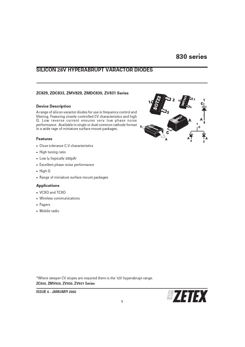
ZC829, ZDC833, ZMV829, ZMDC830, ZV831 Series Device DescriptionA range of silicon varactor diodes for use in frequency control and filtering.Featuring closely controlled CV characteristics and high Q.Low reverse current ensures very low phase noise performance.Available in single or dual common cathode format in a wide rage of miniature surface mount packages.Features·Close tolerance C-V characteristics ·High tuning ratio ·Low I R (typically 200pA)·Excellent phase noise performance ·High Q·Range of miniature surface mount packagesApplications·VCXO and TCXO·Wireless communications ·Pagers ·Mobile radio*Where steeper CV slopes are required there is the 12V hyperabrupt range.ZC930, ZMV930, ZV930, ZV931 Series 830 seriesISSUE 6 - JANUARY 20021SILICON 28V HYPERABRUPT VARACTOR DIODES830 seriesISSUE 6 - JANUARY 20022PARTCapacitance (pF)V R =2V,f=1MHzMin Q V R =3V f=50MHzCapacitance RatioC 2/C 20at f=1MHzMIN.NOM.MAX.MIN.MAX.829A 7.388.29.02250 4.3 5.8829B 7.798.28.61250 4.3 5.8830A 9.010.011.0300 4.5 6.0830B 9.510.010.5300 4.5 6.0831A 13.515.016.5300 4.5 6.0831B 14.2515.015.75300 4.5 6.0832A 19.822.024.2200 5.0 6.5832B 20.922.023.1200 5.0 6.5833A 29.733.036.3200 5.0 6.5833B 31.3533.034.65200 5.0 6.5834A 42.347.051.7200 5.0 6.5834B 44.6547.049.35200 5.0 6.5835A 61.268.074.8100 5.0 6.5835B 64.668.071.4100 5.0 6.5836A 90.0100.0110.0100 5.0 6.5836B95.0100.0105.0100 5.06.5TUNING CHARACTERISTICS at Tamb = 25°CPARAMETER SYMBOLMAX UNIT Forward currentI F 200mA Power dissipation at T amb =25ЊC SOT23P tot 330mW Power dissipation at T amb =25ЊC SOD323P tot 330mW Power dissipation at T amb =25ЊC SOD523P tot250mW Operating and storage temperature range-55to +150ЊCABSOLUTE MAXIMUM RATINGSPARAMETERCONDITIONS MIN.TYP.MAX.UNIT Reverse breakdown voltage I R =10uA 25V Reverse voltage leakageV R =20V 0.220nA Temperature coefficient of capacitanceV R =3V,f =1MHz300400ppCm/ЊCELECTRICAL CHARACTERISTICS at Tamb = 25°C830 seriesTYPICAL CHARACTERISTICSISSUE 6 - JANUARY 20023830 seriesISSUE 6 - JANUARY 20024O R D E R C O D E S A N D P A R T M A R K I N GR E E L C O D ER E E L S I Z ET A P E W I D T HQ U A N T I T Y P E R R E E LT A7i n c h (180m m )8m m3000T C13i n c h (330m m )8m m 10000T A P E A N D R E E L I N F O R M A T I O NT h e o r d e r c o d e s a r e s h o w n a s T A w h i c h i s f o r 7i n c h r e e l s .F o r 13i n c h r e e l s s u b s t i t u t e T C i n p l a c e o f T A i n t h e o r d e r c o d e .ISSUE 6 - JANUARY 20025830 seriesSOT23 PACKAGE DIMENSIONSSOD323 PACKAGE DIMENSIONSZetex plcFields New Road ChaddertonOldham, OL9 8NP United KingdomTelephone (44) 161 622 4422Fax: (44) 161 622 4420Zetex GmbHStreitfeldstraße 19D-81673 München GermanyTelefon: (49) 89 45 49 49 0Fax: (49) 89 45 49 49 49Zetex Inc700 Veterans Memorial Hwy Hauppauge, NY11788USATelephone: (631) 360 2222Fax: (631) 360 8222Zetex (Asia) Ltd3701-04Metroplaza, Tower 1Hing Fong Road Kwai Fong Hong KongTelephone: (852) 26100 611Fax: (852) 24250 494These offices are supported by agents and distributors in major countries world-wide.This publication is issued to provide outline information only which (unless agreed by the Company in writing)may not be used,applied or reproduced for any purpose or form part of any order or contract or be regarded as a representation relating to the products or services concerned.The Company reserves the right to alter without notice the specification,design,price or conditions of supply of any product or service.For the latest product information,log on to©Zetex plc 2001830 series6ISSUE 6 - JANUARY 2002DIM MILLIMETRES MIN.MAX A ᎏ0.800A10.0000.100A20.6000.800b10.1600.300c 0.0800.220D 0.7000.900E 1.500 1.700E1 1.100 1.300L 0.2000.400L10.1700.230⍜1Њ4Њ10ЊSOD523 PACKAGE DIMENSIONSSOD323 PACKAGE DIMENSIONS。
机场视频监控系统及安防集成

机场视频监控系统及安防集成2009-04-14 11:27:13 作者:深圳市博康系统工程有限公司宋绍锋黄鹰来源:安防技术与设计第25期近年来随着我国经济的高速增长,航空运输得到了迅猛的发展,全国各大枢纽机场进入了新一轮的改、扩建高潮,特别为了保障奥运会的需要,首都机场T3航站楼、上海浦东机场T2航站楼率先完成了扩建。
今年以来,国家为刺激经济作出了四万亿的巨大投资计划,其中机场等交通基础设施是重点投入领域,这必将带来新机场和机场扩建的新高潮。
鉴于国内外反恐形势的日益严峻,机场空防以及运行管理的需要,机场安防系统的建设得到了前所未有的重视。
同时安防技术也在快速发展,正逐步由模拟监控系统向数字监控系统过渡。
而数字化的安防技术为与机场其它业务系统的集成提供了更好的技术支撑。
本文从机场视频监控系统的建设、特点,并围绕机场用户的实际需要,阐述了数字视频监控系统的设计架构、建设模式、与门禁报警、智能化及机场业务系统的集成等,为机场安防系统的建设提供了一种借鉴。
一、机场监控系统的建设模拟监控系统和数字视频监控系统是安防监控系统中的两大技术体系。
模拟系统具有系统延时小、设备成熟等优点。
但当系统矩阵规模超过一定限度时,就会出现矩阵扩容设备呈几何级增长,多级联网造成图像质量急剧下降,且不能直接使用计算机进行视频浏览、管理,不便于视频资源共享等缺点。
数字视频监控系统具有扩容方便、资源易于共享、适于构建大型分布系统、便于分析、管理和更易于集成等特点。
目前在安防监控行业使用得比较成熟、稳定的视频压缩标准,主要有MPEG-2、MPEG-4及H.264,近两年支持H.264压缩算法的编解码器产品进步很快,逐渐获得了用户的青睐。
现代化的机场作为安防系统应用的一个重要行业,其对于集成的要求远远高于其它行业,因此数字化、网络化的安防系统更能符合机场的业务需求。
目前国内最大的两个机场首都机场T3和浦东机场T2都采用了数字化的安防监控系统。
QLogic QLE7340单口40GbpsQDR InfiniBand PCIe 2.0 X8主机

QLogic QLE7340 Single-Port 40 Gbps QDR InfiniBand Host Channel AdapterProduct Guide (withdrawn product)High-performance computing (HPC) solutions have used InfiniBand networks to meet the needs of the most demanding sets of applications and grand challenges. The QLE7340 is a single-port 40 Gbps InfiniBand PCI Express Gen2 x8 host channel adapter (HCA). It is a highly integrated design that delivers a high message rate and low latency, making it the ideal solution for HPC applications.Figure 1 shows the QLogic QLE7340 single-port 4X QDR IB PCIe 2.0 X8 host channel adapter.Figure 1. QLogic QLE7340 Single-Port 40 Gbps QDR InfiniBand HCADid you know?Click here to check for updatesDid you know?The QLogic QLE7340 HCA is part of IBM Intelligent Cluster solution (formerly IBM Systems Cluster 1350). IBM Intelligent Cluster is your key to a fully integrated HPC solution. IBM clustering solutions include servers, storage, and industry-leading OEM interconnects that are factory-integrated, fully tested, and delivered to your door, ready to plug into your data center, all with a single point of contact for support.Part number informationTable 1. Ordering part numbers and feature codesDescription Part number Feature code QLogic QLE7340 Single-Port 40 Gbps QDR InfiniBand HCA59Y188857630.5 m QLogic Copper QDR InfiniBand QSFP 30AWG Cable59Y189237251 m QLogic Copper QDR InfiniBand QSFP 30AWG Cable59Y189637263 m QLogic Copper QDR InfiniBand QSFP 28AWG Cable59Y190037273 m QLogic Optical QDR InfiniBand QSFP Cable59Y1920373110 m QLogic Optical QDR InfiniBand QSFP Cable59Y1924373230 m QLogic Optical QDR InfiniBand QSFP Cable59Y192837333m IBM Optical QDR InfiniBand QSFP Cable49Y0488598910m IBM Optical QDR InfiniBand QSFP Cable49Y0491599030m IBM Optical QDR InfiniBand QSFP Cable49Y04945991 Features and benefitsSupported serversThe QLogic QLE7340 HCA is supported in the IBM System x servers listed in Table 2 as part of the IBM Intelligent Cluster portfolio.Table 2. Supported servers in the IBM Intelligent Cluster portfolioQLogic QLE7340 HCA5763Y Y Y Y Y Y Y Y N N N N N Popular configurationsPopular configurationsFigure 2 illustrates how the QLogic QLE7340 HCA can be used in configurations. In this example, weconnect all InfiniBand HCAs to a QLogic 12200 QDR InfiniBand switch.Figure 2. x3650 M2 server with the QLogic QLE7340 HCA connected to an InfiniBand networkThe parts used are listed in Table 3.Table 3. Components used when connecting QLogic QLE7340 HCA to an InfiniBand network (Figure 2)Diagram reference Partnumber/machinetypeDescriptionQuantity Varies x3650 M2 or other supported server (See Table 2.)1 59Y1888QLogic QLE7340 HCA1 Varies QLogic QDR InfiniBand QSFP Cable, copper or optical (SeeTable 1.)1 0449-020QLogic 12200 (iDPx) 36-port QDR InfiniBand Switch Bundle1Supported operating systemsTrademarksLenovo and the Lenovo logo are trademarks or registered trademarks of Lenovo in the United States, other countries, or both. A current list of Lenovo trademarks is available on the Web athttps:///us/en/legal/copytrade/.The following terms are trademarks of Lenovo in the United States, other countries, or both:Lenovo®Intelligent ClusterSystem x®The following terms are trademarks of other companies:Linux® is the trademark of Linus Torvalds in the U.S. and other countries.Other company, product, or service names may be trademarks or service marks of others.。
ad834使用手册

ad834使用手册引言:AD834是一款广泛应用于通信领域的集成电路芯片,它是一款高性能、高精度的多功能模数转换器。
本手册将为读者提供有关AD834的基本信息以及使用指南,帮助用户更好地了解和使用这款芯片。
一、AD834的基本介绍AD834是一款由Analog Devices公司设计和生产的集成电路芯片。
它具备了多种功能,包括模拟信号的放大、变换以及数字信号的处理,广泛应用于通信系统、无线电设备以及雷达等领域。
AD834的设计高度集成化,可以实现高度精确的信号处理和转换,大大简化了系统设计和调试的难度,提高了整体性能。
二、AD834的主要特性1. 高性能模数转换器:AD834具有高分辨率和高采样率的模数转换功能,可以对模拟信号进行快速、精确的采样和转换,输出数字信号供后续处理。
2. 宽带放大器:AD834内置了宽带放大器电路,可以放大模拟信号的幅度,满足不同应用场景下对信号放大的需求。
3. 低噪声传输:AD834采用了先进的低噪声技术,减少了信号在转换过程中的噪声干扰,提供了清晰、稳定的信号传输。
4. 调制和解调功能:AD834具备先进的调制和解调功能,可以将模拟信号转换为数字信号,或将数字信号转换为模拟信号,满足不同通信系统的需求。
5. 多种输出接口:AD834支持多种输出接口,包括模拟输出、数字输出和串行接口,方便与其他设备进行连接和数据交互。
三、AD834的使用指南1. 电源连接:使用AD834之前,首先需要正确连接芯片的电源。
通常,AD834需要提供正负供电电压,确保电源电压的稳定和合适的范围。
2. 信号输入和输出连接:根据不同的应用需求,将输入信号与AD834的输入端口相连,并将输出端口与下游电路或设备进行连接。
3. 控制参数设置:AD834提供了一些控制参数,可以通过相应的控制寄存器进行设置。
对于不同的应用场景,用户可以根据需求调整这些参数,以优化模数转换的性能和适应特定的信号处理需求。
常见PHY芯片品牌介绍

常见PHY芯片品牌介绍2008-01-07 11:39目前市场上百兆交换机是一个非常成熟的产品,各个芯片公司对自己的产品都进行了多次的优化和精简。
总的来说规格和性能方面都能满足作为2层傻瓜型交换机的应用。
一些主要的技术指标也基本相同。
所有公司的芯片都可以支持10/100M自适应;全线速交换;支持线序交叉功能。
下面我们将深入分析目前市场上采用的百兆交换机方案:1.Realtek 公司Realtek公司相信大家比较熟悉,市场上百兆网卡大多采用他们公司8139芯片。
作为一个网络低端市场的芯片供应商16口和24口百兆交换机也是他们主推的产品。
Realtek公司百兆交换机方案的芯片型号为:RTL8316 + RTL8208;24口RTL8324 + RTL8208。
Realtek 公司采用的是MAC (媒介控制芯片)与PHY (物理层芯片)相分离的架构。
RTL8316和RTL8324是MAC (媒介控制芯片),RTL8208是8口的PHY (物理层芯片)。
RTL8316集成4 M位DRAM缓存用于数据包存储转发;RTL8324集成4 M位缓存。
这个缓存的大小对于交换机处理数据的能力有着很大的影响!RTL8316和RTL8324 MAC地址表的深度为8K!2.ICPlus 公司ICPlus公司也是台湾一家有着多年历史的网络芯片生产商。
ICPlus公司百兆交换机方案的芯片型号为:IP1726 + IP108。
同样ICPlus公司也采用MAC (媒介控制芯片)与PHY (物理层芯片)相分离的架构。
IP1726是MAC (媒介控制芯片),IP108是8口的PHY (物理层芯片)。
IP1726集成1.5 M位缓存用于数据包存储转发。
IP1726 MAC地址表的深度为4K!3.Admtek 公司Admtek公司今年已经被德国英飞凌公司收购,实际上应该是德国公司。
Admtek公司百兆交换机方案的芯片型号为:ADM6926 + ADM7008。
Pico BTS 242
美国瑞通网络(i roe e o s公司是全面的城域网络 R et t r ) v sn N w k 解决方案提供者,其路由器产品可将城域网络上的原始带宽转 变为可赢利的业务。目前瑞通公司的产品已部署在 4 多个国 0
网络的覆盖及覆盖范围内的信号质量是两个非常重要的方面。
目前, 国内G M运营商的网络在历经多年的充分发展后 , S 已基 本解决了覆盖问题, 从城市、 郊区到农村, 基本上有话务量需求 的地区都已得到了覆盖。而随着网络用户数量的急剧增加,网 络覆盖范围内的信号质量问题变得日益突出了。特别是对室内
产品与市场
Pc T 4 : 门子 室 内和 热 点 地 区 的解ຫໍສະໝຸດ 决 方 案 i B S2 2 西 o
邓学 军
( 海 西 门子 移动 通信 有 限公 司 上 海 2 10 ) 上 026
站分成了两部分: 服务器和代理机。 服务器负责对整个基站的控制、 BC的A i接1 网管、 与 S b 3、 s
1 引 言
移动网络运营商的网络质量是赢得并保留客户,从而使收 益获得稳定增长的基础。在衡量移动网络质量的众多指标中,
告警、 对代理机控制并向代理机提供电压。 代理机实际是将通常基站中的载波单元分离出来,每个代
理机就是一个T X 它与服务器之间用标准双绞线相连, R, 传输距
离最远可达 22 m . 。 k
的发展对宽带化、 多媒体化提出了越来越高的要求,I P网络的 建设也迫切需要一种更为高效的技术,解决服务质量问题以及
家和地区的一些大型网络中。包括英国电信、 韩国电信、和记 环球电讯、中国电信、中国网通、 C Wodo M I r Cm等。近日,美 l
ADS8344中文资料
+4.75V < VCC < 5.25V
SHDN = VDD Data Transfer Only
16
14
15
8
±2
1.2
4
±0.05
1.0
4
20
3
16
4.5
T
100
500
30
100
2.4
0.024
2.4
T
0
2.4
T
DYNAMIC CHARACTERISTICS Total Harmonic Distortion(2) Signal-to-(Noise + Distortion) Spurious Free Dynamic Range Channel-to-Channel Isolation
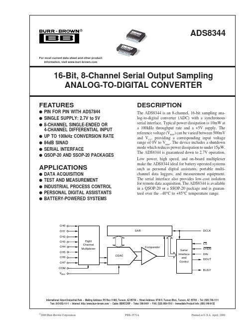
CH0 CH1 CH2 CH3 CH4 CH5 CH6 CH7 COM VREF
Eight Channel Multiplexer
SAR
CDAC
Comparator
Serial Interface
and Control
DCLK
CS SHDN DIN DOUT
BUSY
International Airport Industrial Park • Mailing Address: PO Box 11400, Tucson, AZ 85734 • Street Address: 6730 S. Tucson Blvd., Tucson, AZ 85706 • Tel: (520) 746-1111 Twx: 910-952-1111 • Internet: / • Cable: BBRCORP • Telex: 066-6491 • FAX: (520) 889-1510 • Immediate Product Info: (800) 548-6132
ADS8341E;ADS8341EB;ADS8341EBG4;ADS8341E2K5;ADS8341E2K5G4;中文规格书,Datasheet资料
DESCRIPTION
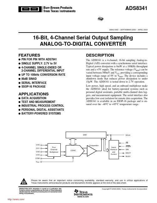
The ADS8341 is a 4-channel, 16-bit sampling Analog-toDigital (A/D) converter with a synchronous serial interface. Typical power dissipation is 8mW at a 100kHz throughput rate and a +5V supply. The reference voltage (VREF) can be varied between 500mV and VCC, providing a corresponding input voltage range of 0V to VREF. The device includes a shutdown mode that reduces power dissipation to under 15µW. The ADS8341 is tested down to 2.7V operation.
Low power, high speed, and an onboard multiplexer make the ADS8341 ideal for battery-operated systems such as personal digital assistants, portable multi-channel data loggers, and measurement equipment. The serial interface also provides low-cost isolation for remote data acquisition. The ADS8341 is available in an SSOP-16 package and is ensured over the –40°C to +85°C temperature range.
ADS8344 芯片在船载气象观测设备中的应用

ADS8344 芯片在船载气象观测设备中的应用作者:于慧彬,李小峰来源:《科技创新与生产力》 2015年第3期于慧彬1,2,李小峰1,2(1. 山东省海洋环境监测技术重点实验室,山东青岛 266001;2. 山东省科学院海洋仪器仪表研究所,山东青岛 266001)摘要:在海洋和大气观测领域,对温湿度等气象参数的观精度要求越来越严格。
文章设计和实现了一种基于ADS8344芯片的用于实时观测温湿度数据的数据采集模块。
该模块采用基于AVR单片机的嵌入式系统集成设计方案,通过ADS8344芯片实现温湿度传感器的信号采集,为船载气象观测设备测量本点的气象信息。
关键词:ADS8344;温湿度测量;数据采集模块;船载气象设备中图分类号:TN79-2 文献标志码:A DOI:10.3969/j.issn.1674-9146.2015.03.062在海洋和大气观测领域,人们对温湿度等气象参数的观精度要求越来越严格。
此次设计的数据采集模块服务于某型船舶气象观测设备,该设备实现了船舶本站各种气象要素实时数据的自动采集观测。
其基本工作原理是通过该设备内部的数据采集模块实时采集外部传感器测量的船舶所处位置的气温、气压、湿度、风速和风向等气象要素观测数据,并进行运算和汇总,实时获得气象观测数据,将处理过的数据分发给其他外部设备,用于辅助船舶航行、气象资料收集及动力定位等应用。
1 数据采集模块的设计文章设计的数据采集模块是一款船用气象观测设备的传感器采样处理模块。
考虑到作为船用观测设备,在进行传感器的输出信号选择时,选用了不易受外界干扰的4~20 mA标准电流信号作为其输出信号[1]。
因此在主机端进行信号采集时,需要在数据采集模块设计硬件A/D采样转换电路,将传感器输出的电流信号转换为数字量,然后通过微处理器进行运算处理。
数据采集模块的A/D采样电路硬件设计主要分为3个部分,分别是微处理器MCU、A/D转换器和参考电源设计[2]。
fod8342光耦参数

fod8342光耦参数FOD8342光耦参数光耦器件是一种将输入和输出电路通过光信号进行隔离的电子元件。
FOD8342是一款常见的光耦器件,具有多种参数和特性。
本文将对FOD8342光耦器件的参数进行介绍和解析。
1. 电气特性FOD8342的电气特性包括输入和输出特性。
输入特性方面,其输入电流为5mA,输入电压为1.5V。
输出特性方面,其输出电流为16mA,输出电压为30V。
这些参数对于设计和选择电路时非常重要,可以根据实际需求来确定使用FOD8342的合适条件。
2. 绝缘特性FOD8342的绝缘特性非常优秀,其绝缘电压可达3750Vrms。
这意味着在使用FOD8342进行信号隔离时,可以有效地阻止输入和输出之间的电流和电压相互干扰,保证了电路的安全性和可靠性。
3. 工作温度范围FOD8342的工作温度范围为-40°C至+105°C。
这个范围适用于各种环境条件下的应用,可以满足大部分工业和商业设备的需求。
4. 封装类型FOD8342采用了DIP-4封装,这种封装形式方便了器件的安装和焊接,使其可以广泛应用于各种电子设备中。
5. 光耦比光耦比是光耦器件的一个重要参数,它表示了输入光功率和输出电流之间的关系。
FOD8342的光耦比为50%,这意味着输入的光功率的50%可以转化为输出电流。
这个参数可以帮助我们评估光耦器件的工作效率和性能。
6. 响应时间FOD8342的响应时间非常短,仅为5微秒。
这意味着它可以在很短的时间内完成输入和输出信号的转换,适用于高速传输和快速响应的应用领域。
7. 电流传输比电流传输比是光耦器件的另一个重要参数,它表示了输入电流和输出电流之间的比例关系。
FOD8342的电流传输比为200%,这意味着输出电流是输入电流的两倍。
这个参数可以帮助我们评估光耦器件的放大能力和信号传输效果。
8. 应用领域由于FOD8342具有优秀的绝缘特性、高速响应和可靠性,它被广泛应用于工业自动化、电力电子、通信设备等领域。
fod8342 典型应用电路

fod8342 典型应用电路典型应用电路是指在实际工程或项目中广泛应用的电路设计。
这些设计已经被验证并有效地解决了特定的问题或满足了特定的需求。
以下是一些常见的典型应用电路和它们的相关参考内容:1. 电源管理电路:电源管理电路通常用于提供稳定可靠的电源供电,以确保其他电路和设备正常工作。
其中一个重要的电源管理电路是稳压电路。
稳压电路的核心是稳压器件,如线性稳压器、开关稳压器等。
可以参考的内容包括:- 《稳压电路设计手册》:介绍了稳压电路的基本原理、设计方法和常见应用。
- 《电源管理设计指南》:详细讲解了电源管理电路的设计、优化和故障排除技巧。
- 《稳压器件手册》:提供了各种稳压器件的参数、应用案例和选型指南。
2. 信号放大电路:信号放大电路用于放大小信号,以便传递、处理或测量。
常用的信号放大电路包括运算放大器(OP-AMP)电路、差分放大器电路等。
相关参考内容包括:- 《运算放大器应用手册》:介绍了运算放大器的基本原理、特性和常见应用电路。
- 《放大器设计指南》:讲解了放大器电路设计的基本原理、技巧和优化方法。
- 《差分放大器设计指南》:详细介绍了差分放大器的设计原理、优化和应用案例。
3. 滤波电路:滤波电路用于去除电信号中的杂波或选择特定频率范围的信号。
常见的滤波电路包括低通滤波器、高通滤波器和带通滤波器等。
相关参考内容包括:- 《滤波器设计手册》:介绍了滤波器的基本原理、设计方法和常见应用。
- 《模拟滤波器设计指南》:详细讲解了模拟滤波器的设计原理、优化和实现技巧。
- 《数字滤波器设计手册》:提供了数字滤波器的设计方法、算法和应用案例。
4. 时钟和定时电路:时钟和定时电路用于生成、分配和同步系统中的时钟信号。
这些电路通常应用于数字系统、通信系统和计算机系统中。
相关参考内容包括:- 《时钟和计时电路设计手册》:介绍了时钟电路和定时电路的设计原理、实现方法和应用实例。
- 《数字系统时钟设计指南》:详细讲解了数字系统中时钟设计的技巧、优化和故障排除方法。
微Focus安全ArcSight连接器智能连接器for IP流信息导出(IPFIX)配置指南June

Micro Focus Security ArcSight ConnectorsSmartConnector for IP Flow Information Export (IPFIX)Configuration GuideJune, 2018Configuration GuideSmartConnector for IP Flow Information Export (IPFIX)June, 2018Copyright © 2016 – 2017; 2018 Micro Focus and its affiliates and licensors.WarrantyThe only warranties for products and services of Micro Focus and its affiliates and licensors (“Micro Focus”) are set forth in the express warranty statements accompanying such products and services. Nothing herein should be construed as constituting an additional warranty. Micro Focus shall not be liable for technical or editorial errors or omissions contained herein. The information contained herein is subject to change without notice.Restricted Rights LegendConfidential computer software. Except as specifically indicated otherwise, a valid license from Micro Focus is required for possession, use or copying. Consistent with FAR 12.211 and 12.212, Commercial Computer Software, Computer Software Documentation, and Technical Data for Commercial Items are licensed to the U.S. Government under vendor's standard commercial license.Trademark NoticesAdobe™ is a trademark of Adobe Systems Incorporated. Microsoft® and Windows® are U.S. registered trademarks of Microsoft Corporation. UNIX® is a registered trademark of The Open Group. Revision HistoryDate Description10/17/2017 Added encryption parameters to Global Parameters.11/30/2016 Updated installation procedure for setting preferred IP address mode.08/30/2016 First release of this connector.Configuration Guide SmartConnector for IP Flow Information Export (IPFIX)This guide provides information for installing the SmartConnector for IP Flow Information Export (IPFIX) and configuring the device for event collection. IPFIX Version 10 is supported. Product OverviewInternet Protocol Flow Information Export (IPFIX) is an IETF protocol and the name of the IETF working group defining the protocol. It was created based on the need for a common, universal standard of export for Internet Protocol flow information from routers, probes, and other devices used by mediation systems, accounting/billing systems, and network management systems to facilitate services such as measurement, accounting, and billing.The IPFIX standard defines how IP flow information is to be formatted and transferred from an exporter to a collector.Similar to the NetFlow protocol, IPFIX considers a flow to be any number of packets observed in a specific timeslot and sharing a number of properties (same source, same destination, and same protocol). Using IPFIX, devices such as routers can inform a central monitoring station about their view of a potentially larger network.IPFIX is a push protocol; each sender will periodically send IPFIX messages to configured receivers without any interaction by the receiver.IPFIX can integrate information that would normally be sent to Syslog or SNMP directly in the IPFIX packet, thus eliminating the need for these additional services collecting data from each network device. This lets hardware vendors specify a Vendor ID and put any proprietaryinformation into a Flow and export it out of the collector/analyzer for further dissecting andmonitoring.IPFIX also allows fields of a variable length, which means IDs do not have to conform to a fixed length. Netflow does not allow variable length fields. Variable length fields let you saveinformation such as URLs (which differ from site to site), messages, HTTP hosts, and more. ConfigurationFor instructions on configuring IPFIX for event collection, see the vendor documentation for your IPFIX-supported device.Install the SmartConnectorThe following sections provide instructions for installing and configuring your selectedSmartConnector.SmartConnector for IP Flow Information Export (IPFIX)Prepare to Install ConnectorBefore you install any SmartConnectors, make sure that the ArcSight products with which the connectors will communicate have already been installed correctly (such as ArcSight ESM or ArcSight Logger).For complete product information, read the Administrator's Guide as well as the Installation and Configuration guide for your ArcSight product before installing a new SmartConnector. If you are adding a connector to the ArcSight Management Center, see the ArcSight Management Center Administrator's Guide for instructions, and start the installation procedure at "Set GlobalParameters (optional)" or "Select Connector and Add Parameter Information."Before installing the SmartConnector, be sure the following are available:⏹Local access to the machine where the SmartConnector is to be installed⏹Administrator passwordsInstall Core SoftwareUnless specified otherwise at the beginning of this guide, this SmartConnector can be installed on all ArcSight supported platforms; for the complete list, see the SmartConnector Product and Platform Support document, available from the Micro Focus SSO and Protect 724 sites.1Download the SmartConnector executable for your operating system from the Micro Focus SSO site.2Start the SmartConnector installation and configuration wizard by running the executable.Follow the wizard through the following folder selection tasks and installation of the coreconnector software:IntroductionChoose Install FolderChoose Shortcut FolderPre-Installation SummaryInstalling...3When the installation of SmartConnector core component software is finished, the following window is displayed:Configuration GuideSet Global Parameters (optional)If you choose to perform any of the operations shown in the following table, do so before adding your connector. You can set the following parameters:Parameter SettingFIPS mode Select 'Enabled' to enable FIPS compliant mode. To enable FIPS Suite B Mode, see theSmartConnector User Guide under "Modifying Connector Parameters" for instructions. Initially, thisvalue is set to 'Disabled'.Remote Management Select 'Enabled' to enable remote management from ArcSight Management Center. When queriedby the remote management device, the values you specify here for enabling remote managementand the port number will be used. Initially, this value is set to 'Disabled'.Remote Management Listener Port The remote management device will listen to the port specified in this field. The default port number is 9001.Preferred IP Version When both IPv4 and IPv6 IP addresses are available for the local host (the machine on which theconnector is installed), you can choose which version is preferred. Otherwise, you will see only oneselection. The initial setting is IPv4.The following parameters should be configured only if you are using Micro Focus SecureData solutions to provide encryption. See the Micro Focus SecureData Architecture Guide for more information.Parameter SettingFormat Preserving Encryption Data leaving the connector machine to a specified destination can be encrypted by selecting ‘Enabled’ to encrypt the fields identified in ‘Event Fields to Encrypt' before forwarding events. If encryption is enabled, it cannot be disabled. Changing any of the encryption parameters again will require a fresh installation of the connector.Format PreservingPolicy URLEnter the URL where the Micro Focus SecureData Server is installed.Proxy Server (https) Enter the proxy host for https connection if any proxy is enabled for this machine.SmartConnector for IP Flow Information Export (IPFIX)Parameter SettingProxy Port Enter the proxy port for https connection if any proxy is enabled for this machine.Format Preserving Identity The Micro Focus SecureData client software allows client applications to protect and access data based on key names. This key name is referred to as the identity. Enter the user identity configured for Micro Focus SecureData.Format PreservingSecretEnter the secret configured for Micro Focus SecureData to use for encryption.Event Fields to Encrypt Recommended fields for encryption are listed; delete any fields you do not want encrypted and add anystring or numeric fields you want encrypted. Encrypting more fields can affect performance, with 20 fieldsbeing the maximum recommended. Also, because encryption changes the value, rules or categorizationcould also be affected. Once encryption is enabled, the list of event fields cannot be edited.After making your selections, click Next. A summary screen is displayed. Review the summary of your selections and click Next. Click Continue to return to proceed with "Add a Connector" window.Continue the installation procedure with "Select Connector and Add Parameter Information." Select Connector and Add Parameter Information1Select Add a Connector and click Next. If applicable, you can enable FIPS mode and enable remote management later in the wizard after SmartConnector configuration.2Select IP Flow Information Export (IPFIX) and click Next.3Enter the required SmartConnector parameters to configure the SmartConnector, then click Next.Configuration GuideParameter DescriptionIPFIX Port Enter the number of the port to which the SmartConnector will listen.IPFIX IP Address The only currently supported value for this field is (ALL), meaning the connector will listen toall IP addresses on the specified port. Individual IP addresses cannot be specified at this time.Select a Destination1The next window asks for the destination type; select a destination and click Next. For information about the destinations listed, see the ArcSight SmartConnector User Guide.2Enter values for the destination. For the ArcSight Manager destination, the values you enter for User and Password should be the same ArcSight user name and password you createdduring the ArcSight Manager installation. Click Next.3Enter a name for the SmartConnector and provide other information identifying the connector's use in your environment. Click Next. The connector starts the registrationprocess.4If you have selected ArcSight Manager as the destination, the certificate import window for the ArcSight Manager is displayed. Select Import the certificate to the connector fromdestination and click Next. (If you select Do not import the certificate to connector fromdestination, the connector installation will end.) The certificate is imported and the Addconnector Summary window is displayed.Complete Installation and Configuration1Review the Add Connector Summary and click Next. If the summary is incorrect, click Previous to make changes.2The wizard now prompts you to choose whether you want to run the SmartConnector as a stand-alone process or as a service. If you choose to run the connector as a stand-aloneprocess, select Leave as a standalone application, click Next, and continue with step 5.3If you chose to run the connector as a service, with Install as a service selected, click Next. The wizard prompts you to define service parameters. Enter values for Service Internal Name and Service Display Name and select Yes or No for Start the service automatically. The InstallService Summary window is displayed when you click Next.4Click Next on the summary window.5To complete the installation, choose Exit and Click Next.For instructions about upgrading the connector or modifying parameters, see the SmartConnector User Guide.SmartConnector for IP Flow Information Export (IPFIX)Run the SmartConnectorSmartConnectors can be installed and run in stand-alone mode, on Windows platforms as aWindows service, or on UNIX platforms as a UNIX daemon, depending upon the platformsupported. On Windows platforms, SmartConnectors also can be run using shortcuts and optional Start menu entries.If the connector is installed in stand-alone mode, it must be started manually and is notautomatically active when a host is restarted. If installed as a service or daemon, the connector runs automatically when the host is restarted. For information about connectors running asservices or daemons, see the ArcSight SmartConnector User Guide.To run all SmartConnectors installed in stand-alone mode on a particular host, open a command window, go to $ARCSIGHT_HOME\current\bin and run: arcsight connectors To view the SmartConnector log, read the file$ARCSIGHT_HOME\current\logs\agent.log; to stop all SmartConnectors, enter Ctrl+C in the command window.Device Event Mapping to ArcSight FieldsThe following section lists the mappings of ArcSight data fields to the device's specific event definitions. See the ArcSight Console User's Guide for more information about the ArcSight data fields.IPFIX Event Mappings to ArcSight ESM FieldsArcSight ESM Field Device-Specific FieldBase Event Count flowsBytes In bytesDestination Address ip_dst_addrDestination Port l4_dst_portDevice Address DeviceAddressDevice Custom IPv6 Address 2 ipv6_src_addr (Source IPV6 Address)Device Custom IPv6 Address 3 ipv6_dst_addr (Destination IPV6 Address)Device Custom Number 1 pkts (packets)Device Custom Number 2 tcp_flags (tcp_flags)Device Custom String 1 ip_next_hop (nexthop)Device Custom String 2 src_as (Source BGP autonomous system number)Device Custom String 3 dst_as (Destination BGP autonomous system number)Device Custom String 4 src_mask (src_mask)Device Custom String 5 dst_mask (dst_mask)Device Custom String 6 tcp_flags descrDevice Event Class Id 'flow'Device Inbound Interface interface_input_snmpDevice Outbound Interface interface_output_snmpConfiguration GuideArcSight ESM Field Device-Specific FieldDevice Product 'IPFIX'Device Receipt Time pkthdr_unix_secsDevice Vendor 'IPFIX'Device Version pkthdr_versionEnd Time last_switchedName 'IPFIX event'Request Url undefined_32769Source Address ip_src_addrSource Port l4_src_portStart Time first_switchedTransport Protocol protocol。
基于网络编码和安全极化码的无线抗窃听传输技术分析

通信网络技术DOI:10.19399/j.cnki.tpt.2023.04.046基于网络编码和安全极化码的无线抗窃听传输技术分析郭 菲(国网北京市电力公司,北京100051)摘要:无线通信本身具有较强的开放性,其信号具有广播性,因此使得合法用户在接受服务的过程中很容易受到非法用户的窃听。
为了解决这一问题,将网络编码和安全极化码相结合,对信源码块进行重新编码,生成内码,再经过计算巴氏参数、信道分集等过程,以安全极化码为外码,保障通信安全,降低窃听的可靠性,进而提高无线抗窃听能力,希望能够对相关工作提供一定帮助。
关键词:网络编码;安全极化码;无线抗窃听传输技术Analysis of Wireless Anti-Eavesdropping Transmission Technology Based on NetworkEncoding and Secure Polarization CodeGUO Fei(State Grid Beijing Electric Power Company, Beijing 100051, China)Abstract: Wireless communication itself has a strong openness, its signal has broadcasting characteristics, so legal users are vulnerable to illegal users in the process of receiving services. In order to solve this problem, the network coding and security polarization code are combined, and the source code block is rewritten. The internal code is generated through the process of calculating Pap parameters and conducting channel diversity. The security polarization code is the external code to ensure the communication security, reduce the reliability of eavesdropping, and then improve the wireless anti-eavesdropping ability. I hope it can provide some help to the relevant work.Keywords: network code; secure polarization code; wireless anti-eavesdropping transmission technology0 引 言极化码技术在提出后,已被广泛应用于各领域无线通信中,是重要的控制信道编码技术。
基于ADS8341与ARM的数据采集模块接口设计

基于ADS8341与ARM的数据采集模块接口设计韩卫洁;陈江锋;董兴;田军【期刊名称】《现代电子技术》【年(卷),期】2014(000)024【摘要】为了对冻土区土壤环境进行实时采集处理和检测,在此选取ADS8341作为A/D转换芯片,STM32F103ZET6芯片作为微处理器,设计并实现了将ADS8341芯片和STM32F103ZET6芯片相结合用于采集土壤环境数据的硬件电路和A/D采集软件控制过程。
经过实际的检测与分析,该设计可以对冻土区土壤进行实时高效的采集、处理以及对数据的保存,以便后期数据的查询和土壤环境总体趋势的预测。
%In order to conduct real⁃time acquisition, processing and detection of the frozen soil environment data, ADS8341 is chosen as A/D conversion chip and STM32F103ZET6 chip as MPU. The data acquisition circuit and A/D acquisi⁃tion software control process based on ADS8341 and STM32F103ZET6 was designed. The actual tested and analyzed results show that the interface circuit can achieve real⁃time effective acquisition,processing and storage of the frozen soil environmentdata,which contribute to the future query of the relevant data and prediction of the trend of soil environment.【总页数】4页(P84-86,89)【作者】韩卫洁;陈江锋;董兴;田军【作者单位】长安大学工程机械学院,陕西西安 710064;长安大学材料科学与工程学院,陕西西安 710064;长安大学工程机械学院,陕西西安 710064;长安大学工程机械学院,陕西西安 710064【正文语种】中文【中图分类】TN964-34【相关文献】1.基于ARM的RFID数据采集模块设计 [J], 杨阳;胡耀光;周玉偈2.基于ARM芯片与数据采集模块的过滤材料完整性测试仪 [J], 戴志巍;张兴华;王正飞;俞健;黄彦3.基于ARM7内核微处理器的嵌入式USB数据采集模块 [J], 鲍玉军;葛康杰;赵梦婷4.基于ADS8364高速数据采集模块接口设计 [J], 刘品;李松岩;徐赫5.基于ARM7的水监测系统数据采集模块设计 [J], 吴雪琴;肖永松因版权原因,仅展示原文概要,查看原文内容请购买。
DS8340系列磁盘阵列技术白皮书(V40)
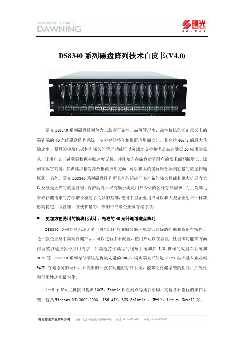
DS8340系列磁盘阵列技术白皮书(V4.0)曙光DS8340系列磁盘阵列包含三款高可靠性、高可管理性、高性价比的真正意义上的端到端的4G光纤磁盘阵列系统,专为存储整合和集群应用而设计。
其高达4Gb/s的最大传输速率、易用的模块化架构和强大的管理功能可以灵活地支持和满足高速数据IO应用的需求,让用户真正感觉到数据存取速度无忧,并且允许存储容量随用户的需求而不断增长。
比如在数字高清、多媒体点播等高数据流应用方面,可以极大的缓解服务器到存储的数据传输瓶颈。
另外,曙光DS8340系列磁盘阵列所具有的超越同类产品的强大性能和超大扩展容量以及领先业界的数据管理、保护功能不仅有助于满足用户今天的各种存储需求,而且为满足未来存储需求的持续增长奠定了良好的基础,使得中型企业用户可以和大型企业用户一样获得高稳定、易管理、方便扩展的可靠的中高端企业级存储系统。
z更加方便易用的模块化设计,先进的4G光纤通道磁盘阵列DS8340系列存储系统为多主机应用和集群服务器环境提供良好的性能和数据有效性,是一款企业级中高端存储产品。
可以进行多种配置,使用户可以在容量、性能和功能等方面作调整以适应各种应用需求,如高速持续读写的视频系统和多I/O 操作的数据库系统和OLTP等。
DS8340系列存储系统是将最先进的4Gb/s端到端光纤信道(FC)技术融入企业级RAID存储系统的设计,开发出的一款多功能的存储系统,能够使存储系统的性能、扩展性和可用性达到最大化。
4-8个4Gb主机接口提供LOOP、Fabric和点到点等拓扑结构,支持各种流行的操作系统:包括Windows NT/2000/2003,IBM AIX、SUN Solaris 、HP-UX、Linux、Novell等。
基于先进的模块化设计,系统在容量和性能方面提供极大的灵活性。
每个机箱占3U空间,可容纳16块硬盘。
随着用户需求的增长,可以方便地连接 4Gb FC JBOD――JB8340FF 来扩展存储容量。
- 1、下载文档前请自行甄别文档内容的完整性,平台不提供额外的编辑、内容补充、找答案等附加服务。
- 2、"仅部分预览"的文档,不可在线预览部分如存在完整性等问题,可反馈申请退款(可完整预览的文档不适用该条件!)。
- 3、如文档侵犯您的权益,请联系客服反馈,我们会尽快为您处理(人工客服工作时间:9:00-18:30)。
ORDERING INFORM来自TIONPRODUCT MAXIMUM INTEGRAL LINEARITY ERROR (LSB) NO MISSING CODES (Bits) PACKAGE– LEAD PACKAGE DESIGNATOR(1) SPECIFIED TEMPERATURE RANGE ORDERING NUMBER TRANSPORT MEDIA, QUANTITY Tape and Reel, 250 Tape and Reel, 2000 Tape and Reel, 250 Tape and Reel, 2000
ADS8342
SBAS277 – MAY 2003
16ĆBit, 250kSPS, 4ĆChannel, Parallel Output ANALOGĆTOĆDIGITAL CONVERTER
FEATURES D True Bipolar Input D Input Signal Range: ±2.5V D 4-Channel Input Multiplexer D Up to 250kSPS Sampling Rate D Selectable 8-Bit or 16-Bit Parallel Interface D 16-Bit Ensured No Missing Codes D Offset: 1mV max D Low Power: 200mW D TQFP-48 Package D Operating Temperature Range: –40°C to +85°C APPLICATIONS D Data Acquisition D Test and Measurement D Industrial Process Control D Medical Instruments D Laboratory Equipment DESCRIPTION
2
/
ADS8342
SBAS277 – MAY 2003
PACKAGE DISSIPATION RATINGS
BOARD Low K PACKAGE PFB RΘJC (°C/W) 19.6 RΘJA (°C/W) 97.5 DERATING FACTOR ABOVE TA ≤ +25°C (mW/°C) 10.256 TA ≤ +25°C POWER RATING (mW) 1282 TA ≤ +70°C POWER RATING (mW) 820 TA = +85°C POWER RATING (mW) 666
Please be aware that an important notice concerning availability, standard warranty, and use in critical applications of Texas Instruments semiconductor products and disclaimers thereto appears at the end of this data sheet.
Lead temperature 1.6mm (1/16 inch) from case for 10 seconds +300 °C (1) Stresses above these ratings may cause permanent damage. Exposure to absolute maximum conditions for extended periods may degrade device reliability. These are stress ratings only, and functional operation of the device at these or any other conditions beyond those specified is not implied.
ADS8342IPFBT ADS8342 ±6 15 TQFP 48 TQFP-48 PFB –40°C to t +85 85°C ADS8342IPFBR ADS8342IBPFBT ADS8342 ±4 16 TQFP 48 TQFP-48 PFB –40°C t to +85 85°C ADS8342IBPFBR (1) For the most current specification and package information, refer to our web site at .
The ADS8342 is a 4-channel, 16-bit analog-to-digital converter (ADC). It contains a 16-bit succesive approximation register (SAR), a capacitor-based ADC with an inherent sample-and-hold circuit, an interface for microprocessor use, and parallel 3-state output drivers. The ADS8342 is specified at a 250kHz sampling rate while dissipating only 200mW of power using a ±5V power supply. The ADS8342 is available in a TQFP-48 package and is ensured over the –40°C to +85°C temperature range.
RECOMMENDED OPERATING CONDITIONS
MIN Supply voltage, +AVDD to AGND Supply voltage, –AVDD to AGND Low-voltage levels Supply voltage, voltage BVDD to BGND Supply voltage, +DVDD to DGND Supply voltage, –DVDD to DGND Reference input voltage Analog input voltage Common voltage Ground differences, AGND to REFGND or BGND or DGND Voltage differences, +DVDD to +AVDD and –DVDD to –AVDD 5V logic levels 4.75 –5.25 2.7 4.5 4.75 –5.25 2.0 –REFIN –0.3 –0.01 –0.01 0 0 0 5 –5 2.5 NOM 5 –5 MAX 5.25 –4.75 3.6 +DVDD 5.25 –4.75 2.55 +REFIN +0.3 0.01 0.01 UNIT V V V V V V V V V V V
ABSOLUTE MAXIMUM RATINGS
over operating free-air temperature range unless otherwise noted(1) ADS8342I Supply voltage, +AVDD to AGND and +DVDD to DGND Supply voltage, –AVDD to AGND and –DVDD to DGND Supply voltage, BVDD to BGND Analog input voltage to AGND Reference voltage, REFIN to AGND Common voltage to AGND Digital input voltage to BGND Ground voltage differences, AGND to REFGND or BGND or DGND Voltage differences, BVDD or +DVDD to AGND Voltage differences, +DVDD to +AVDD and –DVDD to –AVDD Voltage differences, BVDD to DVDD Input current to any pin except supply Power dissipation Operating virtual junction temperature range, TJ Operating free-air temperature range, TA Storage temperature range, TSTG –0.3 to 6 –6 to 0.3 –0.3 to 6 –AVDD – 0.3 to +AVDD + 0.3 –0.3 to +AVDD + 0.3 –0.3 to +0.3 BGND – 0.3 to BVDD + 0.3 –0.3 to 0.3 –0.3 to 6 –0.3 to 0.3 –(+DVDD) to 0.3 –20 to 20 see Package Dissipation Ratings table –40 to +150 –40 to +85 –65 to +150 °C °C °C UNIT V V V V V V V V V V V mA
Copyright 2003, Texas Instruments Incorporated
/
ADS8342
SBAS277 – MAY 2003
This integrated circuit can be damaged by ESD. Texas Instruments recommends that all integrated circuits be handled with appropriate precautions. Failure to observe proper handling and installation procedures can cause damage. ESD damage can range from subtle performance degradation to complete device failure. Precision integrated circuits may be more susceptible to damage because very small parametric changes could cause the device not to meet its published specifications.
