TSMF3710中文资料
UNITRODE UC1710 UC2710 UC3710 数据手册
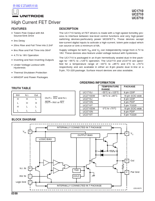
UC1710UC2710UC3710High Current FET DriverFEATURES•Totem Pole Output with 6A Source/Sink Drive •3ns Delay•20ns Rise and Fall Time into 2.2nF •8ns Rise and Fall Time into 30nF •4.7V to 18V Operation•Inverting and Non-Inverting Outputs •Under-Voltage Lockout with Hysteresis•Thermal Shutdown Protection •MINIDIP and Power PackagesDESCRIPTIONThe UC1710family of FET drivers is made with a high-speed Schottky pro-cess to interface between low-level control functions and very high-power switching devices-particularly power MOSFET’s.These devices accept low-current digital inputs to activate a high-current,totem pole output which can source or sink a minimum of 6A.Supply voltages for both V IN and V C can independently range from 4.7V to 18V. These devices also feature under-voltage lockout with hysteresis.The UC1710is packaged in an 8-pin hermetically sealed dual in-line pack-age for –55°C to +125°C operation.The UC2710and UC3710are speci-fied for a temperature range of –40°C to +85°C and 0°C to +70°C respectively and are available in either an 8-pin plastic dual in-line or a5-pin, TO-220 package. Surface mount devices are also available.INV N.I.Out H H L L H H H L L LLLTRUTH TABLEBLOCK DIAGRAMOUT=INV and N.I.OUT=INV or N.I.TEMPERATURE RANGEPACKAGE UC1710J –55°C to +125°C 8 pin CDIPUC2710DW –40°C to +85°C16 pin SOIC-wide UC2710J 8 pin CDIP UC2710N 8 pin PDIP UC2710T 5 pin TO220UC3710DW 0°C to +70°C16 pin SOIC-wide UC3710N 8 pin PDIP UC3710T5 pin TO220ORDERING INFORMATION查询UC2710供应商CONNECTION DIAGRAMS N-Package J-Package T-PackageSupply Voltage, Vin. . . . . . . . . . . . . . . . . . . . . . . . . . .20V. . . . . . . . . . . . . .20V. . . . . . . . . . . . . .20VCollector Supply Voltage, V C. . . . . . . . . . . . . . . . . . . .20V. . . . . . . . . . . . . .20V. . . . . . . . . . . . . .20VOperating Voltage. . . . . . . . . . . . . . . . . . . . . . . . . . . .18V. . . . . . . . . . . . . .18V. . . . . . . . . . . . . .18VOutput Current (Source or Sink)Steady-State. . . . . . . . . . . . . . . . . . . . . . . . . . . . .±500mA. . . . . . . . . . . .±500mA. . . . . . . . . . . . .±1ADigital Inputs. . . . . . . . . . . . . . . . . . . . . . . . . . . .–0.3V-V IN. . . . . . . .–0.3V – V IN. . . . . . . .–0.3V – V INPower Dissipation at Ta=25°C. . . . . . . . . . . . . . . . . . .1W. . . . . . . . . . . . . . .1W. . . . . . . . . . . . . . .3WPower Dissipation at T (Case) = 25°C. . . . . . . . . . . . . .2W. . . . . . . . . . . . . . .2W. . . . . . . . . . . . . .25WOperating Junction Temperature. . . . . . .–55°C to +150°C. . . .–55°C to +150°C. . . .–55°C to +150°CStorage Temperature. . . . . . . . . . . . . . .–65°C to +150°C. . . .–65°C to +150°C. . . .–65°C to +150°CLead Temperature (Soldering, 10 seconds). . . . . . .300°C. . . . . . . . . . . .300°C. . . . . . . . . . . .300°CNote 1: All currents are positive into, negative out of the specified terminal.Note2:Consult Unitrode Integrated Circuits databook for information regarding thermal specificationsand limitations of packages.ABSOLUTE MAXIMUM RATINGSELECTRICAL CHARACTERISTICS:Unless otherwise stated, these specifications apply for V IN= V C= 15V, No load,T A= T J.PARAMETERS TEST CONDITIONS MIN TYP MAX UNITS V IN Supply Current V IN=18V, V C=18V, Output Low2635mAV IN=18V, V C=18V, Output High2130mA V C Supply Current V IN=18V, V C=18V, Output Low 1.5 5.0mAV IN=18V, V C=18V,Output High 5.08mA UVLO Threshold V IN High to Low 3.8 4.1 4.4VV IN Low to High 4.1 4.4 4.8VELECTRICAL CHARACTERISTICS:Unless otherwise stated, these specifications apply for V IN= V C= 15V, No load,T A= T J.PARAMETERS TEST CONDITIONS MIN TYP MAX UNITS UVLO Threshold Hysteresis0.10.30.5V Digital Input Low Level0.8V Digital Input High Level 2.0V Digital Input Current Digital Input = 0.0V–70–4.0µA Output High Sat., V C– V O I O= –100mA 1.35 2.2VI O= –6A 3.2 4.5VOutput Low Sat., V O I O= 100mA0.250.6VI O= 6A 3.4 4.5VThermal Shutdown165°C From Inv., Input to Output (Note 3, 4):Rise Time Delay CL = 03570nsCL = 2.2nF3570nsCL = 30nF3570ns 10% to 90% Rise CL = 02040nsCL = 2.2nF2540nsCL = 30nF85150ns Fall Time Delay CL = 03570nsCL = 2.2nF3570nsCL = 30nF3580ns 90% to 10% Fall CL = 01540nsCL = 2.2nF2040nsCL = 30nF85150ns From N.I. Input to Output (Note 3,4):Rise Time Delay CL = 03570nsCL = 2.2nF3570nsCL = 30nF3570ns 10% to 90% Rise CL = 02040nsCL = 2.2nF2540nsCL = 30nF85150ns Fall Time Delay CL = 03570nsCL = 2.2nF3570nsCL = 30nF3580ns 90% to 10% Fall CL = 01540nsCL = 2.2nF2050nsCL = 30nF85150nsT A= 25°C (Note 5) CL = 03040mA Total Supply Current at 200kHz InputSwitching FrequencyNote: 3. Delay measured from 50% input change to 10% output change.Note: 4. Those parameters with CL= 30nF are not tested in production.Note: 5. Inv. Input pulsed at 50% duty cycle with N.I. Input = 3V. or N.I. Input pulsed at 50% duty cycle with Inv. Input = 0V.UNITRODE CORPORATION7 CONTINENTAL BLVD. • MERRIMACK, NH 03054TEL. (603) 424-2410FAX (603) 424-3460IMPORTANT NOTICETexas Instruments and its subsidiaries (TI) reserve the right to make changes to their products or to discontinue any product or service without notice, and advise customers to obtain the latest version of relevant information to verify, before placing orders, that information being relied on is current and complete. All products are sold subject to the terms and conditions of sale supplied at the time of order acknowledgement, including those pertaining to warranty, patent infringement, and limitation of liability.TI warrants performance of its semiconductor products to the specifications applicable at the time of sale in accordance with TI’s standard warranty. Testing and other quality control techniques are utilized to the extent TI deems necessary to support this warranty. Specific testing of all parameters of each device is not necessarily performed, except those mandated by government requirements.CERTAIN APPLICATIONS USING SEMICONDUCTOR PRODUCTS MAY INVOLVE POTENTIAL RISKS OF DEATH, PERSONAL INJURY, OR SEVERE PROPERTY OR ENVIRONMENTAL DAMAGE (“CRITICAL APPLICATIONS”). TI SEMICONDUCTOR PRODUCTS ARE NOT DESIGNED, AUTHORIZED, OR WARRANTED TO BE SUITABLE FOR USE IN LIFE-SUPPORT DEVICES OR SYSTEMS OR OTHER CRITICAL APPLICATIONS. INCLUSION OF TI PRODUCTS IN SUCH APPLICATIONS IS UNDERSTOOD TO BE FULLY AT THE CUSTOMER’S RISK.In order to minimize risks associated with the customer’s applications, adequate design and operating safeguards must be provided by the customer to minimize inherent or procedural hazards.TI assumes no liability for applications assistance or customer product design. TI does not warrant or represent that any license, either express or implied, is granted under any patent right, copyright, mask work right, or other intellectual property right of TI covering or relating to any combination, machine, or process in which such semiconductor products or services might be or are used. TI’s publication of information regarding any third party’s products or services does not constitute TI’s approval, warranty or endorsement thereof.Copyright © 1999, Texas Instruments Incorporated。
AS3710-BQFP;中文规格书,Datasheet资料

AS3710High Current Power Management Unit for Portable DevicesP ro d uc t B ri ef1 General DescriptionThe AS3710 is a compact System PMU with integrated battery charger and back light driver.The device offers advanced power management func-tions. All necessary ICs and peripherals in a battery powered mobile device are supplied by the AS3710. It features 3 DCDC buck converters as well as 8 low noise LDOs. The different regulated supply voltages are pro-grammable via the serial control interface. 4MHz opera-tion with 1uH coils are reducing cost and PCB space.The three step-up converter generate voltages fore.g.the backlight, classD amplifier, USB host support or LCD display supply. Both constant voltage (for e.g. OLED supply) as well as constant current (white LED backlight) operations with three current sinks are possi-ble. An internal voltage protection is limiting the output voltage in the case of external component failures.AS3710 contains a linear or switching mode Li-Ion bat-tery charger with constant current and constant voltage. The maximum charging current is 1.5A. An integrated battery switch and an optional external switch are sepa-rating the battery during charging or whenever an exter-nal power supply is present. With this switch it is also possible to operate with no or deeply discharged batter-ies. A programmable current limit can be used to control the maximum current used from a USB supply. Addi-tional features are a 30V OV protection and battery tem-perature supervision.The single supply voltage may vary from 2.7V to 5.5V.2 Key FeaturesPower ManagementVoltage Generation⏹ 3 DCDC step down regulators-DVM (0.6V-3.3V;1x 1.2-1.5A, 2x 0.7-1A)-50uA quiescent current-selectable switching frequency (2, 3 or 4MHz)-2A with combined DCDC 2 & 3⏹ 2 analog low noise LDOs, 6 digital LDOs-2x 1.2-3-3V, 6x 0.9-3.3V; 150-300mA-30uA quiescent current (low power mode)⏹ 1 ultra low power always on LDO 2.5V, 10mA ⏹ power supply supervision⏹ 4sec and 8sec emergency shut-down ⏹ stand-by functionHV Backlight Driver⏹ 3x step up with external transistor⏹ voltage control mode and over-voltage protection ⏹ 3 programmable current sinks (max. 40mA)⏹ e.g. 500mA@5V; 40mA@50V⏹ possible external PWM dimming input (DLS, CABC)Battery Charger⏹ prog. trickle charging (25-220mA)⏹ prog. constant current charging (up to 1500mA)⏹ prog. constant voltage charging (3.9V-4.25V)⏹ charger time-out and temperature supervision ⏹ selectable current limitation for USB mode⏹ integrated battery switch & ideal diode (linear mode)⏹ external battery switch control (switching mode)⏹ external 30V OV protectionGeneralSupervisor⏹ automatic battery monitoring with interrupt genera-tion and selectable warning level⏹ automatic temperature monitoring with interruptgeneration and selectable warning and shutdown levelsReal Time Clock⏹ ultra low power 32kHz oscillator ⏹ sec and minute counter, auto wake-up ⏹ selectable alarm (seconds or minutes)⏹ 32kHz clock output to peripheral ⏹ <1uA total power consumption4 General Purpose IOs⏹ 10bit general purpose ADC input ⏹ wake-up/sleep and DVM input ⏹ PWM (DLS, CABAC) dimming input⏹ status output for: charger, low battery, power goodand step-up overcurrent⏹ Q32k clock output ⏹ interrupt output ⏹ PWM output⏹ step-up feedback inputProduct BriefOTP programmable BOOT Sequence ⏹ programmable regulator default voltages ⏹ programmable start-up sequence General Purpose ADC⏹ 10bit resolution⏹ several internal / external sources-VUSB, VSUP, CHGIN, VBAT-GPIOx, CURRx-XOUT32K, SENSEN_SU1-chip temperatureFigure 1. AS3710 Block Diagram Control Interface⏹ I2C control lines, including watchdog⏹ Power-Up input⏹ bidirectional reset, with selectable delay⏹ ultra low power standby modePower-On Reset CircuitPackagingQFN56 7x7mm 0.4mm pitchApplicationPortable Media Players, Portable Navigation Devices,E-Books, Mobile Internet Devices, Tablet PCsProduct Brief - Ke y F e at u re sCopyrightCopyright © 20110.20, austriamicrosystems AG, Schloss Premstaetten, 8141 Unterpremstaetten, Austria-Europe. Trademarks Registered ®. All rights reserved. The material herein may not be reproduced, adapted, merged, trans-lated, stored, or used without the prior written consent of the copyright owner.All products and companies mentioned are trademarks or registered trademarks of their respective companies. DisclaimerDevices sold by austriamicrosystems AG are covered by the warranty and patent indemnification provisions appearing in its Term of Sale. austriamicrosystems AG makes no warranty, express, statutory, implied, or by description regarding the information set forth herein or regarding the freedom of the described devices from patent infringement. austria-microsystems AG reserves the right to change specifications and prices at any time and without notice. Therefore, prior to designing this product into a system, it is necessary to check with austriamicrosystems AG for current informa-tion. This product is intended for use in normal commercial applications. Applications requiring extended temperature range, unusual environmental requirements, or high reliability applications, such as military, medical life-support or life-sustaining equipment are specifically not recommended without additional processing by austriamicrosystems AG for each application. For shipments of less than 100 parts the manufacturing flow might show deviations from the standard production flow, such as test flow or test location.The information furnished here by austriamicrosystems AG is believed to be correct and accurate. However, austriamicrosystems AG shall not be liable to recipient or any third party for any damages, including but not limited to personal injury, property damage, loss of profits, loss of use, interruption of business or indirect, special, incidental or consequential damages, of any kind, in connection with or arising out of the furnishing, performance or use of the tech-nical data herein. No obligation or liability to recipient or any third party shall arise or flow out of austriamicrosystems AG rendering of technical or other services.Contact InformationHeadquartersaustriamicrosystems AGA-8141 Schloss Premstaetten, AustriaTel: +43 (0) 3136 500 0Fax: +43 (0) 3136 525 01For Sales Offices, Distributors and Representatives, please visit:/contact分销商库存信息: AMSAS3710-BQFP。
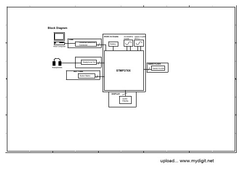
Sigmatel STMP3710方案MP3电路原理图
PREV
B
NEXT
VOL+
VOL-
LCD_CS LCD_RS LCD_RESET LCD_WR LCD_BUSY LCD_RD PWM0 PWM1 PWM2 PWM3 PWM4
28 41 42 43 27 44 91 87 83 84 82
LCD_CS LCD_RS LCD_RESET LCD_WR LCD_RD VDDIO_P
"Menu" & USB Recovery Mode
SW2 R3 1K PSWITCH SW PUSHBUTTON R4 100K 10%
VDDXTAL
GND 73 68 67 VDDXTAL REFP VAG
C
VDDXTAL
"Power/Play/ Pause Button"
C29 0.1uF
C30 0.1uF GND
Y2 32.768kHz 30ppm C36 XpF C37 XpF
RTC_XTALI RTC_XTALO
I2C_SDA I2C_SCL ROTARYB ROTARYA
80 81 25 24
R18 R19
0/NC 0/NC
I2C_SDA I2C_SCL
D18 LED
D17 LED
D10 LED
D12 LED
The 24 MHz crystal should be located close to the STMP37XX. Consult crystal manufacturer datasheet for recommended load capacitor values (typically 10-18pF). Cload = [ (C26*C27) / (C26+C27) ] + Cstray where Cstray = stray PCB capacitance, typically 4 - 6 pF Note: For Microsoft DRM applications use a 30 ppm crystal. NOTE: The crystal load capacitors C26 and C27, should be resized appropriately when STFM1000 is connected to the crystal circuit. Note that STFM1000 TB2 has 1-2 pF of internal capacitance.
37103510系列37113511系列

光纤通讯传输系统用户手册Infinova目录注意事项 (1)产品描述 (2)订购信息 (3)安装 (3)电源 (4)发射机面板 (6)迷你发射机面板 (7)接收机面板 (8)典型系统连接图 (9)网管功能 (10)浪涌保护 (11)注意事项本产品应由专业的技术人员安装。
非专业人员请勿擅自安装操作。
如果在产品的安装过程中需要相关信息或服务,请和当地供应商联系,或者请拨打Infinova客户服务专线:1-732-355-9100,51 Stouts Lane, Monmouth Junction, NJ 08852 U.S.A。
注意:在返送任何产品进行维修前,请务必索取返修授权号码和填写货运通知单。
在该保证书中我们的责任只限于对我们的产品进行维修或替换,条件是产品在规定的额定值和应用范围内使用,及产品按照标准的工程准则使用,并且产品经过我们的检验证明是存在缺陷的。
由于意外,误用,滥用,疏忽,不合法的应用或安装,不合法的操作或维修,连接到不正确的电源电压或已改变的材料,或在非Infinova授权的维修中心进行维修的任何Infinova产品不在此保证书之列。
由美国Infinova公司提供的信息准确可靠。
但是,对于信息的使用,或对于由信息的使用可能导致的对第三方其它权利的任何侵害,Infinova一概不承担责任。
Infinova 公司的任何专利或专利权均不以暗示或其它方式颁发许可证。
警告:本产品应严加保护,防火,防震,谨防雨淋,谨防在潮湿环境中工作!通电状态下请勿向光学端口内观看,以免损伤眼睛!产品描述描述3710/3711和3510/3511系列光端机是在一根光纤上传输数字编码复合视频信号的高质量高可靠性光纤传输系统。
模块兼容PAL 、SECAM 和NTSC 视频信号。
即插即用的设计确保安装简便,无需电气或光学调节。
每台发射机或接收机都配置有状态指示灯,用于指示系统的运行状况。
该系列光端机提供独立式,插卡式和迷你型发射机三款供选择。
SAMSON3730-3智能型电气阀门定位器样本

系列型电气阀门定位器带通信应用型单作用或双作用阀门定位器用于装配到气动控制阀,自校准、自动适配控制阀和气动执行机构。
输入控制信号至行程至开启角度至数字式电气阀门定位器作为气动控制阀的重要附属装置,接受控制系统或控制器输出的电动控制信号,按预先设置关系辅助气动执行机构调整阀位并实现准确定位。
阀门定位器将从控制系统接收的输入控制信号(给定参数)和控制阀位行程或旋转角(被调参数)反馈量进行比较、处理,进而输出相应的气动控制信号(输出参数)给气动执行机构。
特点•易于安装到所有直行程和角行程执行机构上。
-直接集成安装(图)-连接(图)-直接安装在符合标准的杆型支架上-按照标准连接-按标准连接角行程气动执行机构(图)•可安装在任意位置(非悬空)•简单的单旋钮按键、菜单驱动操作•显示、可在任意安装位置选择任何方向读取•使用软件、经串行接口由机进行组态•可变的自动启动具有四种不同的初始化模式•预置参数-只需调整偏离标准的数值•校准后的行程传感器不受机械传动机构磨损的影响•在紧急情况下,同时生产现场不允许控制阀进行全行程动作时,使用“”初始化模式(替换法)对阀门定位器进行替换后的启动•所有参数永久存储在存储器(电源故障保护)•二线制系统,负载电阻为Ω•输出信号压力限值可调•可激活紧急关闭功能•零点连续监视•集成工作温度传感器和运行时间计数器•标配有两个可组态的阀位报警•自诊断;按照建议规范,报警为缩写状态,通过故障报警接点或可选的模拟阀位变送器送出•集成自诊断软件(见)相关产品信息表年月版数据表图:型直接装配到型气动执行机构图:型装配到凸缘图:型按照标准装配图:型带分体式阀位传感器和型微流量控制阀类型-型数字式电气阀门定位器,现场操作、就地通信使用接口,自诊断、通信。
-型数字式电气阀门定位器,现场操作、就地通信使用接口,自诊断、压力传感器用于监控气源和信号压力附加可选-感应式阀位开关(接近开关)-二线制模拟信号的阀位变送器-电磁阀强制排气功能-二进制输入-分体式阀位传感器(图)-模拟输入-不锈钢外壳-泄漏传感器监控阀座泄漏工作原理型数字式电气阀门定位器装配到气动控制阀。
德森印刷机说明书
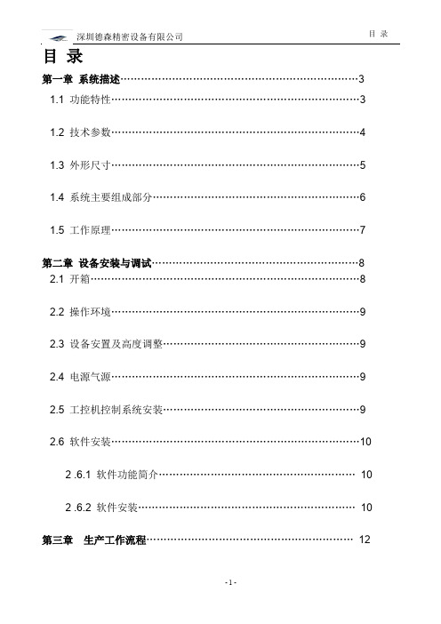
深圳德森精密设备有限公司目录目录第一章系统描述 (3)1.1 功能特性 (3)1.2 技术参数 (4)1.3 外形尺寸 (5)1.4 系统主要组成部分 (6)1.5 工作原理 (7)第二章设备安装与调试 (8)2.1 开箱 (8)2.2 操作环境 (9)2.3 设备安置及高度调整 (9)2.4 电源气源 (9)2.5 工控机控制系统安装 (9)2.6 软件安装 (10)2 .6.1 软件功能简介 (10)2 .6.2 软件安装 (10)第三章生产工作流程 (12)3.2 开始生产前准备 (12)3.2.1范本的准备 (12)3.2.2 锡膏准备 (13)3.2.3 PCB定位调试 (13)3.2.4 刮刀的安装 (14)3.2.5 刮刀压力和速度的选择 (14)3.2.6 脱模速度和脱模长度 (15)3.3试生产 (15)3.4生产流程图 (16)第四章操作系统说明 (17)4.1 系统启动 (17)4.2 主窗口组成 (17)4.2.1归零操作 (17)目录4.2.2主菜单栏 (19)4.2.3主工具栏 (20)4.4 主菜单使用说明 (20)4.4.1打开 (20)4.4.2保存 (21)4.4.3 I/O检测 (21)4.4.4移动检测 (22)4.4.5过板 (23)4.4.6报警复位 (23)4.4.7联机 (23)4.4.8产量清零 (23)4.4.9刮刀移动 (23)4.4.10机器参数 (24)4.4.11更新有效期 (24)4.4.12系统密码 (24)4.4.13密码设置 (24)4.4.14语言 (24)第一章 系统描述4.4.15设置用户产品信息及生产信息 (24)4.4.16查看报警记录 (25)4.4.17生产记录 (25)4.4.18说明 (25)4.4.19故障查询 (26)4.4.20关于DESEN (26)4.5 主工具栏使用说明 (27)4.5.1资料录入 (27)4.5.2生产设置 (31)4.5.3网板自动清洗 (32)4.5.4开始生产 (32)4.5.5停止生产 (33)第一章 系统描述1.1功能特性采用先进的图像视觉识别系统,独立控制与调节的照明,高速移动的镜头,精确地进行PCB 与模板的对准,确保印刷精度为±0.025mm 。
IRFP3710中文资料
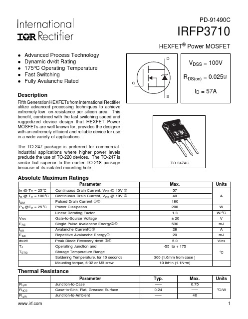
IRFP3710HEXFET ® Power MOSFETFifth Generation HEXFETs from International Rectifier utilize advanced processing techniques to achieve extremely low on-resistance per silicon area. This benefit, combined with the fast switching speed and ruggedized device design that HEXFET Power MOSFETs are well known for, provides the designer with an extremely efficient and reliable device for use in a wide variety of applications.The TO-247 package is preferred for commercial-industrial applications where higher power levels preclude the use of TO-220 devices. The TO-247 is similar but superior to the earlier TO-218 packagebecause of its isolated mounting hole.l Advanced Process Technology l Dynamic dv/dt Ratingl 175°C Operating Temperature l Fast SwitchinglFully Avalanche RatedDescriptionParameterMax.UnitsI D @ T C = 25°C Continuous Drain Current, V GS @ 10V 57I D @ T C = 100°C Continuous Drain Current, V GS @ 10V 40A I DMPulsed Drain Current 180P D @T C = 25°C Power Dissipation 200W Linear Derating Factor 1.3W/°C V GS Gate-to-Source Voltage± 20V E AS Single Pulse Avalanche Energy 530mJ I AR Avalanche Current28A E AR Repetitive Avalanche Energy 20mJ dv/dt Peak Diode Recovery dv/dt 5.0V/ns T J Operating Junction and-55 to + 175T STGStorage Temperature RangeSoldering Temperature, for 10 seconds 300 (1.6mm from case )°CMounting torque, 6-32 or M3 srew10 lbf•in (1.1N•m)Absolute Maximum RatingsParameterTyp.Max.UnitsR q JC Junction-to-Case–––0.75R q CS Case-to-Sink, Flat, Greased Surface 0.24–––°C/WR q JAJunction-to-Ambient–––40Thermal Resistance 1PD-91490CIRFP3710IRFP3710IRFP3710IRFP3710IRFP3710IRFP3710IRFP3710。
TM-xa系列 计重型 收银系列使用说明书V2.30B
1.4 规格 ................................................................................................................. 6 1.5 TM-xA 系列热敏打印机 .................................................................................. 6
前言
感谢您使用上海精函有限公司的产品!在您开始使用本产品前,请务必仔细阅读《前言》中的内容, 并严格遵守这些事项!
1.1 注意事项
Ø 确保电源插头和电源线连接正常,使用三芯电源线进行连接,如果使用了拖线板,则拖线板的插口 也要是三芯的,确保三芯的地线妥善的与建筑大地连接,以避免漏电的情况。
Ø 切勿用沾湿的手插拔电源插头,这样可能导致触电。 Ø 严禁将身体重力压在秤盘上,以免损坏称重传感器。 Ø 严禁撞击重压,或用重物冲击秤盘,以免损坏称重传感器,同时勿超过其最大称量范围。 Ø 严禁淋雨或用水冲洗;如不慎沾水,请用干布擦试干净;若秤体工作异常,请尽速送到经销商处,
3710气动反向放大器安装操作说明
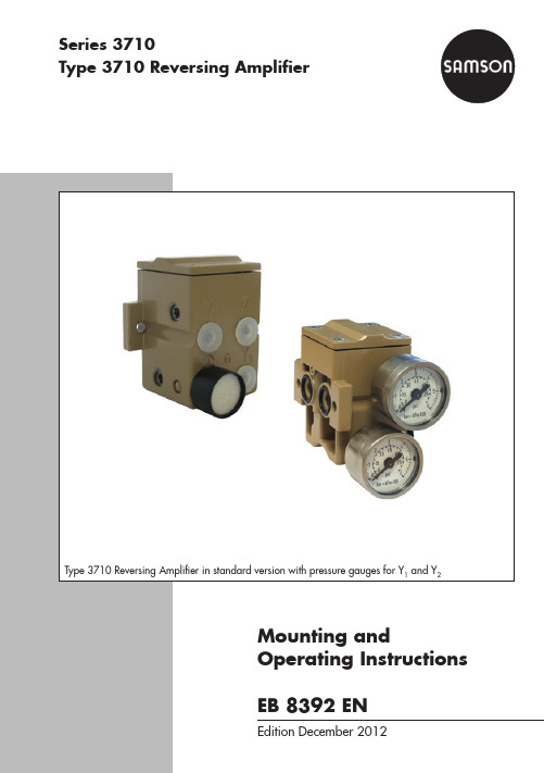
Type 3710 Reversing Amplifier in standard version with pressure gauges for Y 1 and Y 2Series 3710Type 3710 Reversing AmplifierDefinition of signal wordsDANGER!Hazardous situations which, if not avoided, will result in death or seri-ous injuryWARNING!Hazardous situations which, if not avoided, could result in death or seri-ous injuryNOTICEProperty damage message or mal-functionNote:Additional information Tip:Recommended action2 EB 8392 ENNote on these mounting and operating instructionsThese mounting and operating instructions (EB) assist you in mounting and operating the de -vice safely. The instructions are binding for handling SAMSON devices.ÎFor the safe and proper use of these instructions, read them carefully and keep them forlater reference. ÎIf you have any questions about these instructions, contact SAMSON's After-sales Servicedepartment (aftersalesservice@samson.de).Referenced documentationThe documents for the devices used in combination with the reversing amplifier apply in ad -dition to these mounting and operating instructions.The mounting and operating instructions for all supplied devices are included in the delivery. The latest versions of the documents are available on our website at www.samson.de > Prod -uct documentation.ContentsEB 8392 EN 31 General safety instructions .............................................................................42 Markings on the device .................................................................................52.1 Article code ...................................................................................................52.2 Nameplate ....................................................................................................53 Design and principle of operation ..................................................................63.1 Technical data ...............................................................................................73.2 Materials .......................................................................................................74 Attachment to positioners and limit switches ...................................................84.1 Attachment to positioners and limit switches (device index .05 and higher) .........84.2 Attachment to positioners and limit switches (below device index .05) ................84.3 Attachment to Type 3725 Positioner .................................................................84.4 Note on attachment to rotary actuators according to VDI/VDE 3845 ...............104.5 Attachment with Type 4708-54 Supply Pressure Regulator ...............................114.5.1 Note on attachment to Type 3275 Piston Actuator...........................................125 Pneumatic connections .................................................................................125.1 Pressure gauges ...........................................................................................126 Malfunctions ...............................................................................................147 Accessories for Type 3710 (168)Dimensions in mm (17)General safety instructions1 General safety instructionsFor your own safety, follow these instructions concerning the mounting, start-up, and opera-tion of the device:−The device is to be mounted, started up or operated only by trained and experienced personnel familiar with the product. According to these mounting and operating instruc-tions, trained personnel refers to individuals who are able to judge the work they are as-signed to and recognize possible dangers due to their specialized training, their knowl-edge and experience as well as their knowledge of the applicable standards.To avoid damage to any equipment, the following also applies:−Proper shipping and storage are assumed.4 EB 8392 ENMarkings on the device2 Markings on the deviceArticle code2.11Article code2Production ID3Permissible ambient temperature4Configuration IDEB 8392 EN 5Design and principle of operation3 Design and principle of oper-ationThe reversing amplifier allows double-acting pneumatic actuators to be operated using single-acting positioners or limit switches. The positioner creates an output signal pres-sure Y1, to which the air pressure Y2 is add-ed. The reversing amplifier uses the supply pressure Z as auxiliary power.The following rule applies:Y1 + Y2 = ZExample:Y1 of the positioner1 bar Supply pressure Z6 bar Resulting Y25 bar6 EB 8392 ENDesign and principle of operationEB 8392 EN 78 EB 8392 ENAttachment to positioners and limit switches4 Attachment to positioners and limit switchesThe description in section 4.1 and 4.2 ap -plies to the following devices: −Type 3730 Positioner −Type 3731 Positioner −Type 3766 Positioner −Type 3767 Positioner −Type 3768 Limit SwitchÎCheck device index before attachment.Note:See the last two figures of the config -uration ID written on the nameplate for the device index.4.1 Attachment to positionersand limit switches (device index .05 and higher)1. Fasten the reversing amplifier directly tothe positioner/limit switch using two M5 screws. ÎOn mounting the device, make sure thatthe two O-rings (1.2 in Fig. 2 left) are in -serted properly into their groove.Tip:If you lose any O-rings for the revers-ing amplifier, you can order more (order number 8421-9064).4.2 Attachment to positionersand limit switches (below device index .05)Required accessories:Connecting plate (1400-9621) (2 in Fig. 2)1. Screw the special nuts (1) included in theaccessories for the connecting plate (2) into the holes of the positioner.2. Insert the O-rings (1.2) into the groovesof the connecting plate (2). Slide the hol -low bolts (1.3) into the threaded ports and fasten tight.3. Fit O-rings (1.2) on the reversing amplifi -er. Place it on the connecting plate (2) and fasten tight.4.3 Attachment to Type 3725PositionerRequired accessories:Connecting plate (1402-0512) (1 in Fig. 3)1. Fasten the connecting plate (1) betweenthe positioner and the reversing amplifier using two M5 x 50 screws (2).Note:The screws supplied with the connect-ing plate have a TORX PLUS ® profile and must be tightened using a suit-able tool.Attachment to positioners and limit switchesY1Y21.41Special nuts1.2O-rings1.3Hollow bolts1.4Fastening holes2Connecting plateEB 8392 EN 9Attachment to positioners and limit switches4.4 Note on attachment torotary actuators accordingto VDI/VDE 3845The description applies to the following de-vices:−Type 3730 Positioner (angle of rotation >90°)−Type 3766 Positioner−Type 3767 Positioner−Type 3768 Limit SwitchÎFor the attachment of the reversing am-plifier to the above listed devices withmounting kit 1400-8815, remove thevent plug (6) from the intermediate piece(5) and insert into the positioner (seeFig. 4):1. Place the O-ring (3) onto the screw plug(1).2. Screw the screw plug (1) into the ventopening of the intermediate piece (5).3. Thread the threaded bushing (2) and re-taining washer (4) into the free cablegland of the positioner.4. Screw vent plug (6) into the threadedbushing (2).5. Fasten the reversing amplifier directly tothe positioner/limit switch using two M5 screws.Note:The vent plug included in the mount-ing kit (1400-8815) has IP 54 de-gree of protection. For a higher de-gree of protection, select a suitablevent plug from the accessories listedin section 7.10 EB 8392 ENAttachment to positioners and limit switches4.5 Attachment withType 4708-54 Supply Pres-sure RegulatorRequired accessories: Bolts with special nuts (1400-7806) (1 in Fig. 6)1. Screw special nuts (1) into the holes inthe reversing amplifier.2. Insert gasket (3) into the recess of thesupply pressure regulator and slide thespecial hollow bolts (2) into the holes for Output and Supply.3. Position reversing amplifier and fastenusing the hollow bolts (2).Fig. 5: Reversing amplifier with supplypressure regulator mounted ontopositioner and rotary actuatorEB 8392 EN 1112 EB 8392 ENPneumatic connections4.5.1 Note on attachment toType 3275 Piston Actu-atorWhen mounting the reversing amplifier with the Type 4708-54 Supply Pressure Regulator and positioner onto a Type 3275 Piston Ac -tuator:ÎMount the positioner in such a mannerthat the pneumatic connections are lo -cated on the left side (Fig. 7).The supply pressure regulator can only be mounted onto the reversing amplifierin this mounting position.Fig. 7: Type 3710 Reversing Amplifier,Type 4708-54 Supply PressureRegulator with Type 3730 Positioner mounted on Type 3275 Piston Actuator5 Pneumatic connectionsThe air connections are designed either with ¼-18 NPT or G ¼ threads. Customary fit -tings for metal or copper tubing or plastic hoses can be used.Signal pressure connectionsÎSee dimension diagram on page 15for connections ÎY 1: Connect output Y 1 to the signalpressure connection on the actuator that causes the valve to open when the pres -sure rises. ÎY 2: Connect output Y 2 to the signalpressure connection on the actuator that causes the valve to close when the pres -sure rises.5.1 Pressure gaugesThe Type 3710 Reversing Amplifier is de -signed with connections for two pressure gauges on both sides. The connections are sealed with screw plugs G 1/8 when a pres -sure gauge is not installed.Y 1Y 2Fig. 8: The pressure gauges indicate the signalpressure at the outputs.MalfunctionsTechnical dataMounting the pressure gauges1. Remove the screw plug G 1/8 from the re-versing amplifier.2. Insert the seals supplied with the revers-ing amplifier.3. Screw the pressure gauges into the corre-sponding connections.4. Tighten the lock nuts of the pressuregauges leaving a 2 to 3 mm gap be-tween the lock nut and pressure gauge’s square end.ÎAlways use screw plugs G 1/8 to seal any unused pressure gauge connections.6 MalfunctionsThe reversing amplifier is maintenance-free.ÎIf there is leakage between reversing am-plifier and pneumatic connections, check the pipe fittings for leaks.ÎIf there is leakage between reversing am-plifier and positioner, check correct seat-ing of O-rings and replace them withnew ones, if necessary.ÎIn case of other malfunctions, contact SAMSON's After-sales Service depart-ment: aftersalesservice@samson.deEB 8392 EN 13Accessories for Type 37107Accessories for Type 371014 EB 8392 ENDimensions in mm 8 Dimensions in mmEB 8392 EN 15SAMSON AG · MESS- UND REGELTECHNIKWeismüllerstraße 3 · 60314 Frankfurt am Main, Germany Phone: +49 69 4009-0 · Fax: +49 69 4009-1507samson@samson.de · www.samson.deEB 8392 EN2017-01-18 · E n g l i s h。
3710和3720型气动位器和3722型电-气转换器
3710和3720型气动位器和3722型电-气转换器图1. 定位器3710型气动定位器和3720型电-气定位器(图1)被设计用来和薄膜或活塞式旋转执行机构配合使用。
这些定位器能够按特定的输入信号使阀球或阀板停留在特定位置。
3710型定位器能根据气压输入信号使阀门停留在相应位置。
3720型定位器由3722型电-气转换器(图2)和3710型定位器组合而成。
3720型定位器能根据一个直流电流输入信号使阀门停留在相应位置。
与旋转执行机构配合使用时,两种定位器都能很容易地被用于单作用或双作用形式。
2002年8月气源接口W6144 / IL安装在费希尔1052型执行机构上的3720型定位器安装在费希尔1066型执行机构上的3720型定位器W6058-1 / IL输入接口外接地螺钉图2. 3722型电-气转换器W6145 / IL1/2-NPT或M20导线管连接D2437X12规格可用配置3710型: ■单作用或■双作用气动旋转阀门定位器3720型: ■单作用或■双作用电-气旋转阀门定位器由3710型和3722型组成3722型: 一个电-气转换器,将4-20mA直流输入信号转换成供气动定位器使用的0.2-1.0 bar(3-15 psig)气动信号输入信号(1)3710型:标准:■0.2-1.0 bar (3-15 psig)或■0.4-2.0 bar(6-30 psig)分程控制:■0.2-0.6 bar (3-9 psig)和0.6-1.0 bar(9-15 psig)或■0.4-1.2 bar(6-18 psig)和1.2-2.0 bar(18-30psig)3720型:标准: ■4-20mA直流电流且不超过30V的平稳直流电压。
分程使用: ■4-12mA直流电流或12-20mA直流电流。
等效电路3720型: 120欧姆,用3个5.6伏齐纳二极管并联输出信号(1)输出气动压力为执行机构所需最大气压。
作用方式(2): 可在气动阀门定位器上现场进行■正作用和■反作用之间调换。
北洋打印机BTP-L540H(ARM9) 用户手册V1.0

-1-
安全须知
BTP-L540H 用户手册
在使用打印机之前,请仔细阅读下面的注意事项。 1. 安全警告
警告:打印头为发热部件,打印过程中和打印刚结束 时,不要触摸打印头以及周边部件;
警告:不要触摸打印头表面和连接接插件,以免因静 电损坏打印头。
2. 注意事项
1) 打印机应安装在一个平整、稳固的地方;
2) 在打印机的周围留出足够的空间,以便操作和维护;
3) 打印机应远离水源并避免阳光、强光和热源的直射;
4) 避免在高温、高湿以及污染严重的地方使用和存放打印机;
5) 避免将打印机放在有振动和冲击的地方;
6) 避免打印机的表面结露,如果已经形成,在露水消除之前不
要打开打印机的电源;
7) 将打印机的电源连接到一个适当的接地插座上。避免与大型
BTP-L540H 标签打印机
用户手册
山东新北洋信息技术股份有限公司
声明
BTP-L540H 用户手册
本手册内容未经同意不得随意更改,山东新北洋信息技术股
份有限公司(以下简称新北洋)保留在技术、零部件、软件和硬
件上变更产品的权利。用户如果需要与产品有关的进一步信息,
可与新北洋或经销商联系。
未经新北洋的书面许可,本手册的任何章节不得以任何形式、
电机或其它能够导致电源电压波动的设备使用同一插座;
8) 如果较长时间不使用打印机,请断开打印机的电源;
9) 避免水或导电的物质(例如:金属)进入打印机内部,一旦
发生,请立即关闭电源;
10) 避免在无纸状态下打印,否则将严重损害打印胶辊和打印头;
11) 为了保证打印质量和产品的寿命,建议采用推荐的或同等质
3 打印机调节 ............................................................................................ 19 3.1 传感器位置调节 ............................................................................. 19 3.2 打印机常用参数调整 ..................................................................... 20 3.2.1 打印机常用参数的调整及调整范围....................................... 20
TRF3710EVM;中文规格书,Datasheet资料
User's GuideSLAU224–July2007This is the user’s guide for the TRF3710EVM.The TRF3710is a receiver direct downconvert quadrature demodulator that includes programmable baseband filters,adjustable dc offset correction,and buffer amplifiers to directly drive ADCs.The device is suited for operation with CDMA and WCDMA modulation as well as with WiMAX™signals.Contents1Introduction (2)1.1EVM Frequency Configuration Options (2)1.2System Block Diagram (2)2Software Control (2)2.1Installation Instructions (2)2.2Software Operation (2)3EVM Test Configuration (4)3.1Test Block Diagram (4)3.2Test Equipment (5)3.3Calibration (5)4Basic Test Procedure (5)4.1Initial Inspection (5)4.2DC Test (5)4.3Basic RF Test (6)4.4Advanced RF Test (6)5Optional Configurations (8)5.1Mixer Outputs (8)5.2Common Mode Voltage (8)5.3DC Offset Control (8)5.4Analog Gain Control (8)5.5Analog Device Disable (8)List of Figures1System Block Diagram (2)2TRF3710GUI Front Panel (4)3Test Set-up Block Diagram (4)4TRF371x With ADS5232WiMAX3.5MHz Signal EVM Performance (7)List of Tables1Frequency Allocations (5)WiMAX is a trademark of WiMAX Forum CORPORATION.SLAU224–July2007TRF3710EVM1 Submit Documentation Feedback Introduction1Introduction1.1EVM Frequency Configuration OptionsThe TRF3710device is inherently broadband;however,the RF input and LO input require differentialinput which is generally achieved with the use of an RF balun.The EVM can be configured with a different balun to facilitate operation in the desired band.Inspect the board at R101,R102,and R103to determine which balun is populated on the board.1.2System Block DiagramThe basic radio system block diagram in Figure1demonstrates where the TRF3710fits in the overallreceiver.The bold box highlights the TRF3710device.Figure1.System Block Diagram2Software Control2.1Installation Instructions•Open folder named TRF3710_GUI_Installer_Verxpx.fdr(xpx represents the latest version)•Run Setup.exe•Follow the on-screen instructions•Once installed,launch by clicking on the TRF3710_GUI program•When plugging in the USB cable for the first time,the user is prompted to install the USB drivers.–When a pop-up screen opens,select Continue Downloading.–Follow the on screen instructions to install the USB drivers–If needed,the user can access the drivers directly in the install directory2.2Software OperationThe front panel control is shown in Figure2.The registers are set in their default configuration.Thefunctionality of the control registers below.2TRF3710EVM SLAU224–July2007Submit Documentation Feedback2.2.1Register0 2.2.2Register12.2.3Register2 2.2.4Misc Settings Software Control•BB Gain:Sets the gain of the PGA(Programmable Gain Amplifiers);range is0to24.•BBFreq Ctrl:Sets the bandwidth of the BB filters.Setting7is generally suited forWCDMA applications.Setting90is generally suited for CDMAapplications.See data sheet for comprehensive curves.•PWD_Mix/LO/Buf1/Filt/Buf2:Enables SW controlled power down of respective stages inside device.•DC Offset Cal:Selects source for common mode voltage adjustment;Digital settingallows internal registers to fulfill this function.•Cal Reset:Resets the internally stored dc offset values for I and Q back to128.•Readback:If On,it allows the Readback to be enabled.•Readback En:When On,the internal I and Q DAC DC offset settings are readback(only in Auto Cal=Auto mode)•Auto Cal Manual mode allows the DC offset DACs to be user configurable;Auto modeuses the internally stored values.•Auto Cal En:When toggled,an Auto Cal is initiated.Note,Auto Cal must be in Auto mode.•I/Q DAC:Shows the setting of the dc offset I and Q DAC;range is0to255.•I/Q Det:Selects the resolution of the I and Q DAC.•Cal Clk Sel:Toggle between using an externally supplied SPI clock or internal oscillator clock.•Osc.Freq.Selects the oscillator frequency for the internal clock.•Clk Div:Sets the clock divider if the control clocks need to be slowed down.•Mxr I/QOffA/B:Selects the mixer gain for the differential BB paths.Typically,these registersneed no modification.•Reset USB:Toggle this button if the USB port is not responding.This generates a new USBhandle address.•Write Regs:The registers are all written after each modification in the front panel;however,the user can toggle this button to ensure all the registers are loaded as seen onthe screen.•Show Bytes:Shows the32-bit word that is sent for each register.•Show Par Port:Shows the USB pin-out selection•Stop:Stops the programSLAU224–July2007TRF3710EVM3 Submit Documentation Feedback3EVM Test Configuration 3.1Test Block DiagramEVM Test ConfigurationFigure 2.TRF3710GUI Front PanelThe test set-up for general testing of the TRF3710is shown in Figure 3.Figure 3.Test Set-up Block DiagramTRF3710EVM4SLAU224–July 2007Submit Documentation Feedback3.2Test Equipment3.3Calibration4Basic Test Procedure 4.1Initial Inspection4.2DC Test Basic Test ProcedureThe following equipment is required for completing RF Testing:•Power Supply with Current Readout Agilent E3631or Equivalent•Signal Generator for input signal Agilent E4438C or Equivalent•Signal Generator for LO signal Agilent E4438C or Equivalent•Spectrum Analyzer Agilent E4440A or Equivalent•Programming ComputerThe RF cables should be good quality RF cables due to the high frequency signals.•Measure the insertion loss of the RF input cable and use this value to compensate for the desired input power.Note,there is approximately1dB of insertion loss for the input traces and balun on the PCBboard.•Measure the insertion loss of the LO input cable and use this value to compensate for the desired LO power.Note,there is approximately1dB of insertion loss for the input traces and balun on the PCBboard.•BB Loss factor:If using the on-board transformers to interface with50-Ωtest equipment,then there is approximately12.3dB of loss associated with the voltage transformation.This section outlines the basic test procedure for testing the EVM.This section is divided into three test sections:DC and Programmability,Basic CW RF,and Advanced RF Testing.The first section requires only power supply with current readout and a computer for programmability.The second section requires basic RF test equipment and basic technical know-how.The third section is for reference and requires specialized equipment and set-up.Only sections one and two are required to ensure basic functionality.Determine which balun device is placed on the board by inspecting which jumper resistor is installed at the R101,R102,and R103locations.This information determines the proper RF frequencies for which the board is set.Table1.Frequency AllocationsBand Frequency Band F_LO F_RF1G91800–2000MHz 1.9GHz 1.9GHz2G4 2.3–2.7GHz 2.4GHz 2.4GHz3G5 3.5–3.8GHz 3.5GHz 3.5GHz•Connect5V to J11;connect ground to J12.•Engage power supplies.•Verify current is365±25mASLAU224–July2007TRF3710EVM5 Submit Documentation Feedback4.3Basic RF Test4.4Advanced RF TestBasic Test Procedure•Inject LO signal at J7at F_LO frequency at pensate for RF cable losses,including about 1dB for input balun and transmission line losses.•Verify USB cable is connected.•Launch TRF3710EVM_GUI.Select Write Regs to verify programming to the board.•Select CLK Div to 256.•Toggle Auto Cal En on the GUI.Verify that no RF signal in present.•Monitor the dc voltage are TP2(IA)and TP7(IB)and between TP10(QA)and TP12(QB)and verify that the dc offset voltage is 0±15mV.•Inject RF signal at J6at F_RF +300kHz at –pensate for cable loss including about 1dB for input transmission line losses and balun.•Connect Spectrum Analyzer at J3(I).•Set Spectrum analyzer center frequency to 300kHz;set span to 500kHz;set reference level to 0dBm;set analyzer to dc coupling.•Measure signal at 300kHz and verify signal at –9.3dBm ±2dB.Note,there is no compensation for transformer loss.•Adjust BB Gain to 20;verify signal reduces 4dB ±1dB.•Switch output cable to J10(Q)and repeat the procedure above.The EVM is equipped with the differential outputs going to a 16:1transformer for interfacing with 50-Ωtest equipment.This configuration is suitable for completing basic RF test evaluation of the device;however,the inherent high pass nature of a transformer will limit performance at frequencies close to dc.As aresult,this configuration is not suitable for analyzing true modulated signals.As an alternative,the ports at J2,J4,J8,J13offer direct access to the driver amp outputs for the differential I and Q signals respectively.Note,these ports can not drive 50-Ωtest equipment directly.For best performance,the connections to the transformer should be severed by removing capacitors C5,C8,C33,C35.These ports can drive into an ADC directly or into a high impedance differential amplifier.These ports are dc coupled to provide the proper common mode offset voltage to the ADC.The typical EVM performance of the device using a modulated 3.5MHz wide WiMAX signal captured by the ADC is shown in Figure 4.6TRF3710EVMSLAU224–July 2007Submit Documentation FeedbackBasic Test ProcedureFigure4.TRF371x With ADS5232WiMAX3.5MHz Signal EVM PerformanceSLAU224–July2007TRF3710EVM7 Submit Documentation Feedback Optional Configurations5Optional Configurations5.1Mixer OutputsThe mixer outputs can be fed directly to the transformers and to ports J5and J9.This can be useful for measuring the RF performance of the mixer itself without the PGAs or filters.This feature is implemented by toggling the PWD_Buf1to ON.5.2Common Mode VoltageThe common mode voltage is set to a static1.5V by a resistor divider network.Note,the common mode voltage are shifted if the input supply is not5V.Alternatively,this is controlled via a resistive pot by:•Removing R11,R12,R17,R18.•Placing0Ωjumper at:R10and R20.•Adjusting pots at R13and R19.When cascading the device with an ADC it may be desirable to feed the common mode voltage from the ADC to the device.This can be accomplished by:•Removing shunt at W1and W3.•Placing ADC common mode voltage at TP8and TP9.5.3DC Offset ControlThe easiest way to manage the dc offset control is to use the Auto Cal function.This is accomplished by selecting Auto Cal to Auto and toggling the Auto Cal En switch.Monitor the dc offset voltage at TP2(IA) and TP7(IB)and between TP10(QA)and TP12(QB)and verify that the procedure worked sufficiently.The user may also select Readback to On and Readback En to On and find the values of the I and QDAC registers on the GUI.If the RF input signal is disengaged during the auto-cal procedure,then the detection filter bandwidth can remain at10MHz and the clock divider can remain at1.The clock divider can be changed to256toprovide sufficient averaging for the detector to yield superior results.If the RF input signal is applied,reduce the detection filter bandwidth to1kHz and increase the clock divider to1024to increase thedetector averaging.Alternatively,this function can be accomplished by manually programming the I and Q DAC registers.Toggle Auto Cal to Manual.Adjust the I and Q DAC registers on the GUI directly.Monitor the dc offset values at TP2(IA)and TP7(IB)and between TP10(QA)and TP12(QB)until the dc offset is as close to0 mV as possible.A third option is to adjust the common mode through an analog voltage.The EVM is equipped with twopots at R6and R24that control this voltage.On the GUI,change the DC Offset Cal to Analog and adjust the pots at R6and R24while monitoring test points at TP2,TP7,TP10,TP12to get dc offset near0mV.5.4Analog Gain ControlThe device is equipped with three bits to control the PGA gain to facilitate an analog gain control loop that does not require the use of SPI.To use this function,set the BBGain on the GUI to17.Then adjust for the last7states through the binary combination of bits B0,B1,B2that can be toggled at DIP switch SW1. 5.5Analog Device DisableThe device can be disabled by removing jumper at W2.8TRF3710EVM SLAU224–July2007Submit Documentation FeedbackEVALUATION BOARD/KIT IMPORTANT NOTICETexas Instruments(TI)provides the enclosed product(s)under the following conditions:This evaluation board/kit is intended for use for ENGINEERING DEVELOPMENT,DEMONSTRATION,OR EVALUATION PURPOSES ONLY and is not considered by TI to be a finished end-product fit for general consumer use.Persons handling the product(s)must have electronics training and observe good engineering practice standards.As such,the goods being provided are not intended to be complete in terms of required design-,marketing-,and/or manufacturing-related protective considerations,including product safety and environmental measures typically found in end products that incorporate such semiconductor components or circuit boards.This evaluation board/kit does not fall within the scope of the European Union directives regarding electromagnetic compatibility,restricted substances(RoHS),recycling (WEEE),FCC,CE or UL,and therefore may not meet the technical requirements of these directives or other related directives.Should this evaluation board/kit not meet the specifications indicated in the User’s Guide,the board/kit may be returned within30days from the date of delivery for a full refund.THE FOREGOING WARRANTY IS THE EXCLUSIVE WARRANTY MADE BY SELLER TO BUYER AND IS IN LIEU OF ALL OTHER WARRANTIES,EXPRESSED,IMPLIED,OR STATUTORY,INCLUDING ANY WARRANTY OF MERCHANTABILITY OR FITNESS FOR ANY PARTICULAR PURPOSE.The user assumes all responsibility and liability for proper and safe handling of the goods.Further,the user indemnifies TI from all claims arising from the handling or use of the goods.Due to the open construction of the product,it is the user’s responsibility to take any and all appropriate precautions with regard to electrostatic discharge.EXCEPT TO THE EXTENT OF THE INDEMNITY SET FORTH ABOVE,NEITHER PARTY SHALL BE LIABLE TO THE OTHER FOR ANY INDIRECT,SPECIAL,INCIDENTAL,OR CONSEQUENTIAL DAMAGES.TI currently deals with a variety of customers for products,and therefore our arrangement with the user is not exclusive.TI assumes no liability for applications assistance,customer product design,software performance,or infringement of patents or services described herein.Please read the User’s Guide and,specifically,the Warnings and Restrictions notice in the User’s Guide prior to handling the product.This notice contains important safety information about temperatures information on TI’s environmental and/or safety programs,please contact the TI application engineer or visitNo license is granted under any patent right or other intellectual property right of TI covering or relating to any machine,process,or combination in which such TI products or services might be or are used.FCC WarningThis evaluation board/kit is intended for use for ENGINEERING DEVELOPMENT,DEMONSTRATION,OR EVALUATION PURPOSES ONLY and is not considered by TI to be a finished end-product fit for general consumer use.It generates,uses,and can radiate radio frequency energy and has not been tested for compliance with the limits of computing devices pursuant to part15of FCC rules,which are designed to provide reasonable protection against radio frequency interference.Operation of this equipment in other environments may cause interference with radio communications,in which case the user at his own expense will be required to take whatever measures may be required to correct this interference.Mailing Address:Texas Instruments,Post Office Box655303,Dallas,Texas75265Copyright©2007,Texas Instruments IncorporatedEVM WARNINGS AND RESTRICTIONSIt is important to operate this EVM within the input voltage range of5V0.5V and the output voltage range of5V0.5V.Exceeding the specified input range may cause unexpected operation and/or irreversible damage to the EVM.If there are questions concerning the input range,please contact a TI field representative prior to connecting the input power.Applying loads outside of the specified output range may result in unintended operation and/or possible permanent damage to the EVM. Please consult the EVM User's Guide prior to connecting any load to the EVM output.If there is uncertainty as to the load specification, please contact a TI field representative.During normal operation,some circuit components may have case temperatures greater than85°C.The EVM is designed to operate properly with certain components above85°C as long as the input and output ranges are maintained.These components include but are not limited to linear regulators,switching transistors,pass transistors,and current sense resistors.These types of devices can be identified using the EVM schematic located in the EVM User's Guide.When placing measurement probes near these devices during operation, please be aware that these devices may be very warm to the touch.Mailing Address:Texas Instruments,Post Office Box655303,Dallas,Texas75265Copyright©2007,Texas Instruments IncorporatedIMPORTANT NOTICETexas Instruments Incorporated and its subsidiaries(TI)reserve the right to make corrections,modifications,enhancements, improvements,and other changes to its products and services at any time and to discontinue any product or service without notice. Customers should obtain the latest relevant information before placing orders and should verify that such information is current and complete.All products are sold subject to TI’s terms and conditions of sale supplied at the time of order acknowledgment.TI warrants performance of its hardware products to the specifications applicable at the time of sale in accordance with TI’s standard warranty.Testing and other quality control techniques are used to the extent TI deems necessary to support this warranty.Except where mandated by government requirements,testing of all parameters of each product is not necessarily performed.TI assumes no liability for applications assistance or customer product design.Customers are responsible for their products and applications using TI components.To minimize the risks associated with customer products and applications,customers should provide adequate design and operating safeguards.TI does not warrant or represent that any license,either express or implied,is granted under any TI patent right,copyright,mask work right,or other TI intellectual property right relating to any combination,machine,or process in which TI products or services are rmation published by TI regarding third-party products or services does not constitute a license from TI to use such products or services or a warranty or endorsement e of such information may require a license from a third party under the patents or other intellectual property of the third party,or a license from TI under the patents or other intellectual property of TI. Reproduction of TI information in TI data books or data sheets is permissible only if reproduction is without alteration and is accompanied by all associated warranties,conditions,limitations,and notices.Reproduction of this information with alteration is an unfair and deceptive business practice.TI is not responsible or liable for such altered rmation of third parties may be subject to additional restrictions.Resale of TI products or services with statements different from or beyond the parameters stated by TI for that product or service voids all express and any implied warranties for the associated TI product or service and is an unfair and deceptive business practice.TI is not responsible or liable for any such statements.TI products are not authorized for use in safety-critical applications(such as life support)where a failure of the TI product would reasonably be expected to cause severe personal injury or death,unless officers of the parties have executed an agreement specifically governing such use.Buyers represent that they have all necessary expertise in the safety and regulatory ramifications of their applications,and acknowledge and agree that they are solely responsible for all legal,regulatory and safety-related requirements concerning their products and any use of TI products in such safety-critical applications,notwithstanding any applications-related information or support that may be provided by TI.Further,Buyers must fully indemnify TI and its representatives against any damages arising out of the use of TI products in such safety-critical applications.TI products are neither designed nor intended for use in military/aerospace applications or environments unless the TI products are specifically designated by TI as military-grade or"enhanced plastic."Only products designated by TI as military-grade meet military specifications.Buyers acknowledge and agree that any such use of TI products which TI has not designated as military-grade is solely at the Buyer's risk,and that they are solely responsible for compliance with all legal and regulatory requirements in connection with such use.TI products are neither designed nor intended for use in automotive applications or environments unless the specific TI products are designated by TI as compliant with ISO/TS16949requirements.Buyers acknowledge and agree that,if they use anynon-designated products in automotive applications,TI will not be responsible for any failure to meet such requirements. Following are URLs where you can obtain information on other Texas Instruments products and application solutions:Products ApplicationsAmplifiers AudioData Converters AutomotiveDSP BroadbandInterface Digital ControlLogic MilitaryPower Mgmt Optical NetworkingMicrocontrollers SecurityRFID TelephonyLow Power Video&ImagingWirelessWirelessMailing Address:Texas Instruments,Post Office Box655303,Dallas,Texas75265Copyright©2007,Texas Instruments Incorporated分销商库存信息: TITRF3710EVM。
IR3710MTRPBF资料
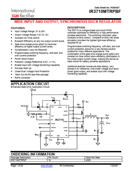
APPLICATION CIRCUIT
Enhanced Gate Drive Application Circuit: V5
D2
D BOOT VIN RFF
D1
V3.3
C1 CPO PVCC FF BOOT UGATE
L C BOOT
6.2k
10k
VCC EN FCCM PGOOD ISET
VOUT
VOUT
IR3710PHASE
LGATE PGND FB
COUT
R1
R ISET
SS
GND
C SS
R2
3.3V Input Voltage Application Circuit:
V3.3
DBOOT NC 6.2k 10k
VCC EN FCCM PGOOD ISET LGATE PGND FB
R FF
IR3710PHASE
LGATE PGND FB
C OUT
R1
RISET
SS
GND
C SS
R2
ORDERING INFORMATION
Package Description IR3710MTRPbF Page 1 of 20 Pin Count 16 IR Confidential Parts Per Reel 4000 1/23/09
元器件交易网
Data Sheet No. PD60367
IR3710MTRPBF
WIDE INPUT AND OUTPUT, SYNCHRONOUS BUCK REGULATOR
FEATURES
Input Voltage Range: 3V to 28V Output Voltage Range: 0.5V to 12V Constant On-Time control Excellent Efficiency at very low output current levels Gate drive charge pump option to maximize efficiency at higher output current levels Compensation Loop not Required Programmable switching frequency, soft start, and over current protection Power Good Output Precision Voltage Reference (0.5V, +/-1%) Enable Input with Voltage Monitoring Capability Pre-bias Start Up Under/Over Voltage Fault Protection 16pin 3x3 MLPQ lead free package RoHS compliant
LINEAR TECHNOLOGY LT3710 说明书

TIME500µs 3710 G081msV GBIASC GBIAS = 2.2µF I GBIAS3710fBOOST (Pin 1): Topside (Boosted) Driver Supply. This pin is used to bootstrap and supply the topside power switch gate drive circuitry. In normal operation V BOOST is powered from the internally generated 8V GBIAS, V BOOST = V SW +8.2V when TGATE is on.TGATE (Pin 2): Topside (Boosted) N-Channel MOSFET Driver. When TGATE is on, the voltage is equal to V SW + 6V.SW (Pin 3): Switch Node Connection to Inductor.CSET (Pin 4): Oscillator Timing Pin. The capacitor on this pin sets the PWM switching frequency.SYNC (Pin 5): Synchronization Input. This pin should be connected to the secondary side output of the power transformer with a series resistor. A filtering capacitor of 10pF is recommended.ILCOMP (Pin 6): Current Limit Amplifier Compensation Node. At current limit, CA1 pulls down on this pin to regulate the output current.SS (Pin 7): Soft-Start. A capacitor on this pin sets the output ramp up rate. The typical time for SS to reach the programmed level is (C • 0.8V)/10µA.V FB (Pin 8): Voltage Amplifier Inverting Input. A resistor divider to this pin sets the output voltage. Nominal voltage at this pin is 0.8V.PI FU CTIO SU U UBGS (Pin 9): Bottom Gate Switching Control. CA2 moni-tors the inductor current and prohibits BGATE from turn-ing on when the inductor current is low (below 8mV across the current sense resistor RS1) to allow discontinous mode operation. Grounding this pin disables comparator CA2.VA OUT (Pin 10): Voltage Amplifier Output.CL + (Pin 11): Current Limit Amplifier Positive Input. The threshold is set at 70mV.CL – (Pin 12): Current Limit Amplifier Negative Input.When used, CL – is connected to the output capacitor side of the current + sense resistor and CL + is connected to the inductor side of the current sense resistor.V CC (Pin 13): Supply of the IC. For proper bypassing, a low ESR capacitor is required.PGND (Pin 14): Ground of the Bottom Side N-Channel MOSFET Driver.BGATE (Pin 15): Bottom Side N-Channel MOSFET Driver.GBIAS (Pin 16): 8V Regulator Output for Boostrapping V BOOST . A bypass capacitor of at least 2µF is needed.Exposed Pad (Pin 17): Connect to PGND (Pin 14).Output N-Channel MOSFET DriversThe LT3710 employs high speed N-channel MOSFET synchronous drivers to achieve high system efficiency.GBIAS is the 8V regulator output to bias and supply the drivers and should be properly bypassed with a low ESR capacitor to ground plane. A Schottky catch diode is required on the switch node.Light Load OperationIf the BGS pin is grounded, the LT3710 stays in continuous mode independent of load condition except in soft-start operation (see Soft-Start section). If the BGS pin is left open, under light load and V RS1 drops below 8mV, BGATE will be turned off(see comparator CA2 of Block Diagram)and the LT3710 goes into discontinous mode operation.Current LimitCurrent limit is set by the 70mV threshold across CL + and CL –, the inputs of the amplifier CA1. By connecting an external resistor RS1(see Block Diagram), the current limit is set for 70mV/R S1. R6 and C6 stablize the current limit loop. If current limit is not used, both CL + and CL –should be grounded and the BGS pin should also be grounded to disable comparator CA2.Soft-Start and ShutdownDuring soft-start, V SS is the reference voltage that controls the output voltage and the output ramps up following V SS .The effective range of V SS is from 0V to V REF . The typical time for the output to reach the programmed level is (C • 0.8V)/10µA.During start up, BGATE will stay off until V SS gets up to 1.6V. This prevents the bottom MOSFET from turning on if the output is precharged.To shut down the LT3710, the SS pin should be pulled below 50mV by a VN2222 type N-channel transistor. Note that during shutdown BGATE will be locked off when V SS drops below 0.6V. This prevents the bottom MOSFET fromAPPLICATIO S I FOR ATIOW UUU discharging the output, which would cause the output to undershoot below yout ConsiderationsFor maximum efficiency, the switching rise and fall times are less than 20ns. To prevent radiation, the power MOSFETs, SW pin and input bypass capacitor leads should be kept as short as possible. A ground plane should be used under the switching circuitry to prevent interplane coupling and to act as a thermal spreading path. Note that the bottom metal of the package is the heat sink, as well as the IC signal ground, and must be soldered to the ground plane.Output Voltage ProgrammingThe feedback reference voltage is 0.8V. The output voltage can be easily programmed by the resistor divider, R3 and R4, as shown in the Block Diagram.V R R OUT208134=+.•Filtering on the SYNC InputIt is necessary to add RC filtering on the SYNC input of the LT3710 to eliminate the negative glitch at the turn on of the top MOSFET. When the top MOSFET M1 turns on, the transformer secondary current instantly changes from the original first output inductor current to the sum of two output inductor currents. The high di/dt on the trans-former leakage inductance causes the transformer sec-ondary voltage V S to drop for a short interval. If the leakage inductance is large enough, the V S dip will be lower than the synchronization threshold (about 2.5V), falsely trig-gering the synchronization. The top MOSFET is turned off immediately. As a result, the output voltage will not be regulated properly.A filter circuit is needed to ensure proper operation. A small RC filter with R S = 10k and C S = 10pF are typical.3710fOutput Inductor SelectionThe key parameters for choosing the inductor include inductance, RMS and saturation current ratings and DCR.The inductance must be selected to achieve a reasonable value of ripple current, which is determined by:∆=−()I V D f LL OUT212••Typically, the inductor ripple current is designed to be 20% to 40% of the maximum output current.The RMS current rating must be high enough to deliver the maximum output current. A sufficient saturation current rating should prevent the inductor core from saturating.These two current ratings can be determined by:I I I I I IRMS O LMAX SAT O LMAX≥+∆≥+∆22122where I O is the maximum output current and ∆I LMAX is the maximum peak-to-peak inductor ripple current.To optimize the efficiency, we usually choose the inductor with the minimum DCR if the inductance and current ratings are the same.Power MOSFET SelectionThe LT3710 drives two external N-channel MOSFETs to deliver high currents at high efficiency. The gate drive voltage is typically 6.5V. The key parameters for choos-ing MOSFETs include drain to source voltage rating V DSS and R DS(ON) at 6.5V gate drive. Note that the transformer secondary voltage waveform will overshoot at its rising edge due to the ringing between transformer leakage inductance and parasitic capacitance. The V DSS of both top and bottom MOSFETs must be sufficiently higher than the maximum overshoot. It is recommended that an RC snubber or a voltage clamping circuitry be placed across the transformer secondary winding to limit the V S overshoot.The R DS(ON) of the MOSFETs should be selected to deliver the required current at the desired efficiency as well as to meet the thermal requirement of the MOSFET package.The conduction power losses of the MOSFETs are:P M1 ≅ I O 2 • R DS(ON)M1 • D2P M2 ≅ I O 2 • R DS(ON)M2 • (1 – D2)where I O is the maximum output current of LT3710 circuit,R DS(ON)M1 and R DS(ON)M2 are the on-resistance for the top and bottom MOSFETs, respectively. The R DS(ON) must be determined with 6.5V gate drive and the expected operat-ing temperature.A good number of high performance power MOSFET selections are available from Siliconix, International Rec-tifier and Fairchild. If the V DSS and R DS(ON) ratings are the same, the MOSFETs with the lowest gate charge Q G should be chosen to minimize the power loss associated with the MOSFET gate drives, the switching transitions and the controller bias supply.Output Capacitor SelectionThe selection of the output capacitor is determined by the output ripple and load transient requirements. In low output voltage applications, always choose capacitors with low ESR. The output ripple voltage is approximated by:∆≈∆+V I ESR fC OUT L OUT 18where ∆I L is the inductor peak-to-peak ripple current.A partial list of low ESR high performance capacitor typesincludes SP capacitors from Panasonic and Cornell Dubilier,POSCAPs and OS-CON capacitors from Sanyo, T510 and T520 surface mount capacitors from Kemet.Design ExampleFigure 3 shows an application example for the LT3710. It is a dual output, high efficiency, isolated DC/DC power supply with 36V to 72V input, 3.3V/10A and 1.8V/10A outputs. The basic power stage topology is a 2-transistorAPPLICATIO S I FOR ATIOW UUULT371011Information furnished by Linear Technology Corporation is believed to be accurate and reliable.However, no responsibility is assumed for its use. Linear Technology Corporation makes no represen-tation that the interconnection of its circuits as described herein will not infringe on existing patent rights.121630 McCarthy Blvd., Milpitas, CA 95035-7417(408) 432-1900 q FAX: (408) 434-0507 q © LINEAR TECHNOLOGY CORPORA TION 2002LT/TP 0803 1K • PRINTED IN USA。
台安S310使用手册

微 处 理 机 控 制 I G B T 推 动交 流 电 机 驱 动 器 使 用 手 册S310系列220V 级0.4~1.5KW (0.88~2.9KVA)地址:江苏省无锡国家高新技术产业开发区65-C号电话: 0510-********(代表号)传真: 0510-********料号:4KA72X201W41为持续改善产品,本公司保留变更设计规格的权利。
S310使用手册目次第零章前言0.1 前言0.2 产品检查第一章安全注意事项1.1 使用时的注意事项1.1.1 送电前1.1.2 送电中1.1.3 运转前1.1.4 运转中1.1.5 检查保养时第二章型号说明第三章使用环境及安装3.1 使用环境3.2 使用环境的注意事项3.3 电磁接触器及电线规格3.3.1 配线应注意事项3.3.2无熔线断路器 / 电磁接触器3.3.3 外围设备的应用及注意事项3.4 规格3.4.1 产品个别规格3.4.2 产品共通规格3.5 S310配线图3.6 变频器端子说明3.7 外型尺寸图第四章软件索引4.1 按键面板使用说明4.2 参数一览表4.3 参数功能说明第五章故障排除及保养5.1故障指示及对策5.1.1 故障指示及对策5.1.2 特殊情况说明5.1.3 按键操作错误说明5.1.4 变频器本体指示灯说明5.2 一般故障检查方法5.3 故障品简单排除步骤0-10-1 1-1 1-1 1-1 1-1 1-1 1-2 1-2 2-1 3-1 3-1 3-2 3-3 3-33-7 3-7 3-7 3-9 3-10 3-12 4-1 4-14-10 5-1 5-1 5-1 5-2 5-25-3 5-4 4-3 3-3 3-4 5-2 0-15.4 日常检查与定期检查5.5 保养与检查第六章外围组件6.1 输入侧交流电抗器规格及制动电阻6.2 操作面板尺寸图及延长线附录一 S310变频器参数设定表5-10 5-11 6-1 6-1 6-1第零章 前言0.1前言为了充分地发挥本变频器的功能及确保使用者的安全,请详阅本操作手册。
青岛海尔洗衣机内桶专机
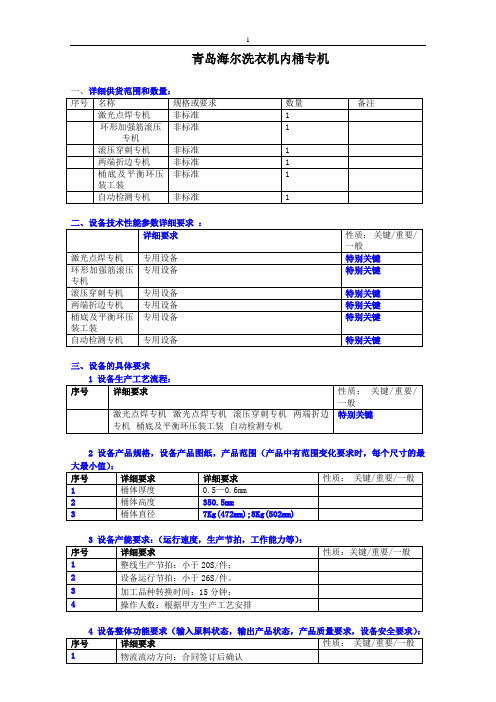
青岛海尔洗衣机内桶专机一、详细供货范围和数量:二、设备技术性能参数详细要求:三、设备的具体要求1 设备生产工艺流程:2 设备产品规格,设备产品图纸,产品范围(产品中有范围变化要求时,每个尺寸的最大最小值):4 设备整体功能要求(输入原料状态,输出产品状态,产品质量要求,设备安全要求):6设备各部分的输入状态,输出状态,质量要求,安全要求,功能和技术要求,以及具体四、设备的总体技术要求:1、设备整体设计和安装质量符合国家相关标准和规范。
符合人机原理:操作方便安全,可最大限度减少工艺动作,降低劳动强度并不会对操作人员的个人身体条件提出高于平常水平的要求。
2设备的设计应充分考虑设备的运行可靠性和无维修设计。
设备运行稳定,故障率低,易于维修维护。
3设备的安装、调整、产品型号更换应方便可靠。
因发生以上工作时,设备不得出现因结构不合理引起的变形或破坏。
4设备设计制造充分考虑了产品质量的稳定性和品种适应性,设备的设计应方便后来的品种增加、型号变换和技术的升级换代。
5设备外型美观,结构工艺合理,安装整齐规范。
6设备的制作外观精良,表面具备良好的防锈处理措施。
油漆要求:喷塑或烤漆。
7 设备要求适合三班制连续运转要求,结构件在设计载荷的2倍范围内可经受非连续冲击不变形不损坏,主要(关键)部件应质量可靠,连续运行12个月内不损坏。
8设备的设计应充分考虑工艺操作和安全生产所需要的各部分控制、启动、急停、连动、连锁、互锁保护、等待等,可最大程度保证生产连续、流畅、均衡进行,可最大限度减少设备因急开急停、工件等待等原因引发的效率和能源损失。
10设备在运行过程中应无异常声音和异常的振动,无异常气味,各部分的温升应符合标准。
润滑装置、油等的过滤装置齐全有效。
设备无跑、冒、滴、漏等问题。
11设备原材料和部件必须选择优质产品,原材料和部件无设计缺陷和加工缺陷。
设计应充分考虑部件的标准化和通用性,不得采用乙方技术独享性质的元器件。
12该设备的设计加工制作是建立在对海尔产品、工艺、工位操作排布、使用条件和环境完全了解的基础上的,并与之相适应。
- 1、下载文档前请自行甄别文档内容的完整性,平台不提供额外的编辑、内容补充、找答案等附加服务。
- 2、"仅部分预览"的文档,不可在线预览部分如存在完整性等问题,可反馈申请退款(可完整预览的文档不适用该条件!)。
- 3、如文档侵犯您的权益,请联系客服反馈,我们会尽快为您处理(人工客服工作时间:9:00-18:30)。
TSMF3710Document Number 81088Rev. 1.3, 21-Feb-07Vishay Semiconductors1948553High Speed Infrared Emitting Diode, 870 nm, GaAlAs Double HeteroDescriptionTSMF3710 is a high speed infrared emitting diode in GaAlAs double hetero (DH) technology in a miniature PLCC-2 SMD package.DH technology combines high speed with high radiant power at wavelength of 870 nm.Features•High radiant power •High speed t r = 30 ns•High modulation band width f c = 12 MHz •Peak wavelength λp = 870 nm •High reliability•Low forward voltage•Suitable for high pulse current application •Wide angle of half intensity•Compatible with automatic placement equipment •EIA and ICE standard package•Suitable for infrared, vapor phase and wavesolder process•8mm tape and reel standard: GS08 or GS18 •Lead (Pb)-free component•Component in accordance to RoH S 2002/95/EC and WEEE 2002/96/ECApplications•High speed IR data transmission•High power emitter for low space applications •High performance transmissive or reflective sen-sorsParts TableAbsolute Maximum RatingsT amb = 25°C, unless otherwise specifiedPartOrdering codeRemarksTSMF3710-GS08TSMF3710-GS08MOQ: 7500 pc TSMF3710-GS18TSMF3710-GS18MOQ: 8000 pcParameterT est conditionSymbol Value Unit Reverse voltage V R 5V Forward current I F 100mA Peak forward current t p /T = 0.5, t p = 100 µs I FM 200mA Surge forward current t p = 100 µsI FSM 1A Power dissipation P V 170mW Junction temperature T j 100°C Operating temperature range T amb - 40 to + 85°C Storage temperature range T stg - 40 to + 100°C Soldering temperature t ≤ 10 secT sd 260°C Thermal resistance junction/ambientR thJA450K/W 2Document Number 81088Rev. 1.3, 21-Feb-07TSMF3710Vishay SemiconductorsBasic CharacteristicsT amb = 25°C, unless otherwise specifiedTypical CharacteristicsT amb = 25°C, unless otherwise specifiedParameterTest conditionSymbol MinTyp.Max Unit Forward voltage I F = 100 mA, t p = 20 ms V F 1.5 1.8V I F = 1 A, t p = 100 µs V F 2.3V Temp. coefficient of V F I F = 100 mA TK VF -2.1mV/K Reverse current V R= 5 VI R 10µA Junction capacitance V R = 0 V , f = 1 MHz, E = 0C j 125pF Radiant intensity I F = 100 mA, t p = 20 ms I e 1022mW/sr I F = 1 A, t p = 100 µs I e 100mW/sr Radiant power I F = 100 mA, t p = 20 ms φe 40mW Temp. coefficient of φe IF = 100 mATK φe -0.35%/K Angle of half intensity ϕ±60deg Peak wavelength I F = 100 mA λp 870nm Spectral bandwidth I F = 100 mA Δλ40nm Temp. coefficient of λp I F = 100 mA TK λp 0.25nm/K Rise time I F = 100 mA t r 30ns Fall timeI F = 100 mAt f 30ns Virtual source size∅0.44mmFigure 1. Power Dissipation vs. Ambient Temperature 05014846P - P o w e r D i s s i p a t i o n (m W )V T am b - Am b ient Temperat u re (°C)Figure 2. Forward Current vs. Ambient Temperature14847I - F o r w a r d C u r r e n t (m A )F T am b - Am b ient Temperat u re (°C)020*********TSMF3710Document Number 81088Rev. 1.3, 21-Feb-07Vishay Semiconductors3Figure 3. Pulse Forward Current vs. Pulse Duration Figure 4. Forward Current vs. Forward Voltage Figure 5. Radiant Intensity vs. Forward Pulse Current0.010.111010100t p - P u lse Length (ms)10095 9985I - F o r w a r d C u r r e n t (m A )F18873I F - F o r w a r d C u r r e n t (m A )1000100101V F - For w ard V oltage (V )24130.11110100100018874I F - For ward P u lse C u rrent (mA)I - R a d i a n t I n t e n s i t y (m W /s r )e Figure 6. Relative Radiant Power vs. WavelengthFigure 7. Relative Radiant Intensity vs. Angular Displacement82087092015821- R e l a t i v e R a d i a n t P o w e re r e l Φ - W a v elength (nm)λ0.4 0.2 0 0.2 0.4 I - R e l a t i v e R a d i a n t I n t e n s i t ye r e l 0.694 80130.60.9 0.8 0°30°10°20°40°50°60°70°80°0.71.0 4Document Number 81088Rev. 1.3, 21-Feb-07TSMF3710Vishay SemiconductorsPackage Dimensions in mmTSMF3710Document Number 81088Rev. 1.3, 21-Feb-07Vishay Semiconductors5Temperature - Time ProfileDrypackDevices are packed in moisture barrier bags (MBB) toprevent the products from moisture absorption during transportation and storage. Each bag contains a des-iccant.Floor LifeFloor life (time between soldering and removing from MBB) must not exceed the time indicated in J-STD-020. TSM... is released for:Moisture Sensitivity Level 2, according to JEDEC, J-STD-020Floor Life: 1 yearConditions: T amb < 30°C, RH < 60 %DryingIn case of moisture absorption devices should be baked before soldering. Conditions see J-STD-020 or Label. Devices taped on reel dry using recommended conditions 192 h at 40°C (+ 5°C), RH < 5 %Figure 8. Lead Tin (SnPb) Reflow Solder ProfileTime (s)T e m p e r a t u r e (°C )250200 150 100 50Figure 9. Blister TapeFigure10. Tape Dimensions in mm for PLCC-2 6Document Number 81088Rev. 1.3, 21-Feb-07TSMF3710Vishay Semiconductors Missing DevicesA maximum of 0.5 % of the total number of compo-nents per reel may be missing, exclusively missing components at the beginning and at the end of the reel. A maximum of three consecutive components may be missing, provided this gap is followed by six consecutive components.The tape leader is at least 160 mm and is followed by a carrier tape leader with at least 40 empty comparte-ments. The tape leader may include the carrier tape as long as the cover tape is not connected to the car-rier tape. The least comoponent is followed by a car-rier tape trailer with a least 75 empty compartements and sealed with cover tape.Cover Tape Removal ForceThe removal force lies between 0.1 N and 1.0 N at a removal speed of 5 mm/s. In order to prevent compo-nents from popping out of the bliesters, the cover tape must be pulled off at an angle of 180° with regard to the feed direction.Figure 11. Beginning and End of ReelFigure12. Dimensions of ReelDe-reeling directionTape leader min.75empty compartments40empty compartmentsCarrier leader Carrier trailer94 8158948665La b el:V Type Gro u pTape Prod u Code Q uTSMF3710Document Number 81088Rev. 1.3, 21-Feb-07Vishay Semiconductors7Ozone Depleting Substances Policy StatementIt is the policy of Vishay Semiconductor GmbH to1.Meet all present and future national and international statutory requirements.2.Regularly and continuously improve the performance of our products, processes, distribution and operating systems with respect to their impact on the health and safety of our employees and the public, as well as their impact on the environment.It is particular concern to control or eliminate releases of those substances into the atmosphere which are known as ozone depleting substances (ODSs).The Montreal Protocol (1987) and its London Amendments (1990) intend to severely restrict the use of ODSs and forbid their use within the next ten years. Various national and international initiatives are pressing for an earlier ban on these substances.Vishay Semiconductor GmbH has been able to use its policy of continuous improvements to eliminate the use of ODSs listed in the following documents.1.Annex A, B and list of transitional substances of the Montreal Protocol and the London Amendments respectively2.Class I and II ozone depleting substances in the Clean Air Act Amendments of 1990 by the Environmental Protection Agency (EPA) in the USA3.Council Decision 88/540/EEC and 91/690/EEC Annex A, B and C (transitional substances) respectively.Vishay Semiconductor GmbH can certify that our semiconductors are not manufactured with ozone depleting substances and do not contain such substances.We reserve the right to make changes to improve technical designand may do so without further notice.Parameters can vary in different applications. All operating parameters must be validated for each customer application by the customer. Should the buyer use Vishay Semiconductors products for any unintended or unauthorized application, the buyer shall indemnify Vishay Semiconductors against all claims, costs, damages, and expenses, arising out of, directly or indirectly, any claim of personaldamage, injury or death associated with such unintended or unauthorized use.Vishay Semiconductor GmbH, P.O.B. 3535, D-74025 Heilbronn, GermanyLegal Disclaimer NoticeVishay Document Number: Revision: 08-Apr-051NoticeSpecifications of the products displayed herein are subject to change without notice. Vishay Intertechnology, Inc., or anyone on its behalf, assumes no responsibility or liability for any errors or inaccuracies.Information contained herein is intended to provide a product description only. No license, express or implied, by estoppel or otherwise, to any intellectual property rights is granted by this document. Except as provided in Vishay's terms and conditions of sale for such products, Vishay assumes no liability whatsoever, and disclaims any express or implied warranty, relating to sale and/or use of Vishay products including liability or warranties relating to fitness for a particular purpose, merchantability, or infringement of any patent, copyright, or other intellectual property right. The products shown herein are not designed for use in medical, life-saving, or life-sustaining applications. Customers using or selling these products for use in such applications do so at their own risk and agree to fully indemnify Vishay for any damages resulting from such improper use or sale.。
