DF3A8.2LFU_07中文资料
SA8382中文资料

SA828 Family
Three-Phase PWM Waveform Generator
DS4226 - 2.0 November 1996
The SA828 PWM generator has been designed to provide waveforms for the control of variable speed AC machines, uninterruptible power supplies and other forms of power electronic devices which require pulse width modulation as a means of efficient power control. The six TTL level PWM outputs (Fig. 2) control the six switches in a three-phase inverter bridge. This is usually via an external isolation and amplification stage. The SA828 is fabricated in CMOS for low power consumption. Information contained within the pulse width modulated sequences controls the shape, power frequency, amplitude, and rotational direction (as defined by the red-yellow-blue phase sequence) of the output waveform. Parameters such as the carrier frequency, minimum pulse width, and pulse delay time may be defined during the initialisation of the device. The pulse delay time (underlap) controls the delay between turning on and off the two power switches in each output phase of the inverter bridge, in order to accommodate variations in the turnon and turn-off times of families of power devices. The SA828 is easily controlled by a microprocessor and its fully-digital generation of PWM waveforms gives unprecedented accuracy and temperature stability. Precision pulse shaping capability allows optimum efficiency with any power circuitry. The device operates as a stand-alone microprocessor peripheral, reading the power waveform directly from an internal ROM and requiring microprocessor intervention only when operating parameters need to be changed. An 8-bit multiplexed data bus is used to receive addresses and data from the microprocessor/controller. This is a standard MOTELTM bus, compatible with most microprocessors/controllers. Rotational frequency is defined to 12 bits for high accuracy and a zero setting is included in order to implement DC injection braking with no software overhead. This family is pin and functionally compatible with the MA828 PWM generator . Two standard wave shapes are available to cover most applications. In addition, any symmetrical wave shape can be integrated on-chip to order.
HYC9088A_07中文资料
HYC9088AARCNET® Twisted Pair and Coaxial Compatible High Impedance Transceiver HIT™FEATURES•ARCNET on Twisted Pair or Coaxial Cable •Drives Shielded and Unshielded Twisted Pair Cable or Coaxial Cable•Compatible with Existing ARCNET Installations • 2.5 Mbps operation •Supports Star, Bus, and Daisy Chained Configurations•Enhanced Built-in Filters for Reduced EMI •Twenty Pin Single In-Line Package •Straight or Right Angle Lead Frame •New Reduced SizeGENERALDESCRIPTIONThe HYC9088A Twisted Pair and Coaxial Compatible High Impedance Transceiver (HIT) is a hybrid module that interfaces an ARCNET Local Area Network controller to one twisted pair or coaxial cable. The HIT interfaces directly with Standard Microsystems Corporation's ARCNET LAN controllers operating at 2.5 Mbps and connects to a variety of shielded and unshielded twisted pair or coaxial cables via an on-board transformer. The network topologies supported by the HIT are daisy chain, star, and bus configurations.During data transmission, the HIT converts the digital pulse information provided by the ARCNET LAN controller into analog signals and drives them onto the cable. The transmitted signals are filtered to eliminate undesirable frequencies. The receiver section of the HYC9088 identifies dipulse signals on the cable and converts them into TTL signals to be supplied to the ARCNET LAN controller.The HIT supports ARCNET's Dipulse Encoding Scheme and, is 100% compatible with all existing coax-based ARCNET networks. This provides an ARCNET network designer with flexibility to easily combine coax and twisted pair cabling.ORDERING INFORMATIONOrder Number(s):HYC9088A R for right angle lead frame leaded packageHYC9088A R-LF for right angle lead frame lead-free RoHS compliant packageSMSC HYC9088A Revision (02-16-07)80 ARKAY DRIVE, HAUPPAUGE, NY 11788 (631) 435-6000, FAX (631) 273-3123Copyright © 2007 SMSC or its subsidiaries. All rights reserved.Circuit diagrams and other information relating to SMSC products are included as a means of illustrating typical applications. Consequently, complete information sufficient for construction purposes is not necessarily given. Although the information has been checked and is believed to be accurate, no responsibility is assumed for inaccuracies. SMSC reserves the right to make changes to specifications and product descriptions at any time without notice. Contact your local SMSC sales office to obtain the latest specifications before placing your product order. The provision of this information does not convey to the purchaser of the described semiconductor devices any licenses under any patent rights or other intellectual property rights of SMSC or others. All sales are expressly conditional on your agreement to the terms and conditions of the most recently dated version of SMSC's standard Terms of Sale Agreement dated before the date of your order (the "Terms of Sale Agreement"). The product may contain design defects or errors known as anomalies which may cause the product's functions to deviate from published specifications. Anomaly sheets are available upon request. SMSC products are not designed, intended, authorized or warranted for use in any life support or other application where product failure could cause or contribute to personal injury or severe property damage. Any and all such uses without prior written approval of an Officer of SMSC and further testing and/or modification will be fully at the risk of the customer. Copies of this document or other SMSC literature, as well as the Terms of Sale Agreement, may be obtained by visiting SMSC’s website at . SMSC is a registered trademark of Standard Microsystems Corporation (“SMSC”). Product names and company names are the trademarks of their respective holders.SMSC DISCLAIMS AND EXCLUDES ANY AND ALL WARRANTIES, INCLUDING WITHOUT LIMITATION ANY AND ALL IMPLIED WARRANTIES OF MERCHANTABILITY, FITNESS FOR A PARTICULAR PURPOSE, TITLE, AND AGAINST INFRINGEMENT AND THE LIKE, AND ANY AND ALL WARRANTIES ARISING FROM ANY COURSE OF DEALING OR USAGE OF TRADE. IN NO EVENT SHALL SMSC BE LIABLE FOR ANY DIRECT, INCIDENTAL, INDIRECT, SPECIAL, PUNITIVE, OR CONSEQUENTIAL DAMAGES; OR FOR LOST DATA, PROFITS, SAVINGS OR REVENUES OF ANY KIND; REGARDLESS OF THE FORM OF ACTION, WHETHER BASED ON CONTRACT; TORT; NEGLIGENCE OF SMSC OR OTHERS; STRICT LIABILITY; BREACH OF WARRANTY; OR OTHERWISE; WHETHER OR NOT ANY REMEDY OF BUYER IS HELD TO HAVE FAILED OF ITS ESSENTIAL PURPOSE, AND WHETHER OR NOT SMSC HAS BEEN ADVISED OF THE POSSIBILITY OF SUCH DAMAGES.Revision (02-16-07)Page 2SMSC HYC9088ADATASHEETRevision (02-16-07) Page 3 SMSC HYC9088ADATASHEETPIN CONFIGURATIONNC NC VDD GND NC VCC R TPA NC TPDPH-B/SHIELD PH-A/CENTER GND GND TPC TPB GND nPULSE2DISABLE nPULSE1PACKAGE: 20-Pin SIPPin 1 DesignatorRevision (02-16-07) Page 4 SMSC HYC9088ADATASHEETDESCRIPTION OF PIN FUNCTIONSPIN NO.NAMESYMBOLDESCRIPTION1, 2, 5, 9 No Connect NCNot used. Make no connection to these pins.3 Power Supply VDD-5 Volts power supply. 4, 13, 14, 17Ground GND Ground. 6 Power Supply VCC+5 Volts power supply.7 Receive Data RXOutput. This signal carries the TTL receive pulse information to the ARCNET LAN Controller Device. 8, 16, 15, 10Test Points TPA, TPB, TPC, TPDTest points. Make no connection to these pins.11 Phase-B/ Shield PH-B/SHIELD Output. Connect this signal to Twisted Pair Connector pin 3 or the shield of the coaxial cable.12 Phase-A/ Center PH-A/ CENTER Output. Connect this signal to Twisted Pair Connector pin 2 or the center of the coaxial cable.18nPulse 2nPULSE2Input. This signal is supplied by the ARCNET LAN Controller Device.19 Disable TX DISABLE TRANSMIT Input. A high level on this signal disables the transmit sectionof the HYC9088. It is normally connected to ground. 20nPulse 1nPULSE1Input. This signal is supplied by the ARCNET LAN Controller Device.Revision (02-16-07) Page 5SMSC HYC9088ADATASHEETFUNCTIONAL DESCRIPTIONThe HYC9088A HIT integrates a host of discrete components into a hybrid module and provides the Local Area Network designer with space and cost savings as well as the enhanced reliability of a single component. Since the HIT is a high impedance transceiver, it does not disturb the characteristic impedance of the cable used to interconnect ARCNET nodes. The two far ends of the twisted pair cable must be terminated using terminating resistors equal to the characteristic impedance of the cable. The HIT is made up of a transmit section and a receive section. (Please refer to Figure 1).Transmit SectionThe ARCNET LAN controller transmits a logic "1" by generating two 100 ns non-overlapping negative pulses, nPULSE1 and nPULSE2. These signals are converted by the HIT into a 200 ns dipulse signal. The HIT shapes the 200 ns signal into a single cycle of a 5 MHz sine-wave and filters higher frequency components. The dipulse signal is then transformer-coupled onto the cable and has a minimum voltage output of 16 Volts peak-to-peak. The exact output voltage of the HIT will vary depending on the characteristic impedance of the cable used. The driving circuitry of the HIT has been designed to present a high impedance on the cable in order to minimize loading.The DISABLE input of the HYC9088 can be used to prevent the device from transmitting. During normal operation, the DISABLE input is tied to ground.Receiver SectionThe received dipulse signal from the cable is electrically isolated through the use of a transformer. This signal is passed through a filter which eliminates out of band noise. The receive signal is then fed to a comparator which converts it into a TTL signal ready to be applied to the LAN controller chip. The comparator compares the received signal to an internal voltage threshold to distinguish noise from real signal.APPLICATION INFORMATIONSmall Twisted Pair NetworksThe HIT eliminates the need for active hubs in small ARCNET networks. For example, a ten node ARCNET network can be constructed by connecting ten HITs using a daisy-chained or bus configuration (see Figure 2). Note that both extremes of the cable must be terminated with a resistor which matches the characteristic impedence of the Twisted Pair Cable. For the cable types specified in Table 1, the maximum length of the twisted pair cable recommended is 400 feet.Small Coax NetworkNo active hub is required for an ARCNET network consisting of eight nodes or less using the HYC9088 for coax cable (See Figure 2A). Both ends of the cable must be terminated with a resistor which matches the characteristic impedance of the coax cable. For the RG62 cable specified in Table 1, the maximum length of the coax cable recommended is 1000 feet.Combination of Twisted Pair and Coax NetworksA Two-Port Link is used to combine twisted pair network and a coax network. A Two-Port Link has a coax connector on one side and two modular jacks on the other and contains the proper impedance-matching circuitry. Refer to Figure 3 for an illustration of a twisted pair network combined with a coaxial network.Revision (02-16-07) Page 6SMSC HYC9088ADATASHEETProper Connection for Twisted PairEach twisted pair compatible ARCNET node would typically have two RJ-11 modular connectors mounted on the node card (refer to Figure 4). PHASE A should be connected to pin 2 of the connectors and PHASE B to pin 3. A twisted pair segment would have an RJ-11 modular jack on each end (see Figure 5). Please note that the suggested numbering scheme of the modular jack shown in Figure 5 may not be consistent with that found on some manufacturers' products. Please ensure consistent connection of Phase A and Phase B signals throughout the network to avoid the reception of erroneous data. Table 1 - Specifications for CablingPARAMETER VALUE FOR COAX VALUE FOR TWISTED PAIR WiringRG62 Solid Copper 22, 24, or 26 AWG Number of Twists/Foot N/A2 min.DC Resistance3.4 Ohms/1000 ft. 28.6 Ohms/1000 ft. max. Characteristic Impedance 93 Ohms at 1 MHz 105 Ohms 20% at 1 MHz Maximum Attenuation 5.5 dB/1000 ft. at 5 MHz16.0 dB/1000 ft. at 5 MHzDISABLERx DA T A+5V GND -5V GND GND GNDAFIGURE 1 – HYC9088A INTERNAL BLOCK DIAGRAMFIGURE 2 – TYPICAL SMALL TWISTED PAIR ARCNET NETWORK USING HYC9088AFIGURE 2A – TYPICAL SMALL COAX ARCNET NETWORK USING HYC9088AFIGURE 3 – TYPICAL COMBINATION OF TWISTED PAIR AND COAXIAL CABLE ON AN ARCNET NETWORKUSING HYC9088ARevision (02-16-07)Page 7SMSC HYC9088ADATASHEETFIGURE 4 – RJ-11 CONNECTORS ON NODE CARDFIGURE 5 – PHASE RELATIONSHIP ON TWISTED PAIR SEGMENT AND RJ-11 CONNECTOR PINOUTRevision (02-16-07)Page 8SMSC HYC9088ADATASHEETFIGURE 6 – TYPICAL HYC9088A INTERCONNECT FOR TWISTED PAIR CABLEFIGURE 7 – TYPICAL HYC9088A INTERCONNECT FOR COAXIAL CABLEFIGURE 8 – DESCRIPTION OF TERMINATOR WIRINGRevision (02-16-07)Page 9SMSC HYC9088ADATASHEETRevision (02-16-07) Page 10 SMSC HYC9088ADATASHEETOPERATIONAL DESCRIPTIONMAXIMUM GUARANTEED RATINGS*Operating Temperature Range.....................................................................................................0o C to +70oC Storage Temperature Range.....................................................................................................-55o to +150o C Lead Temperature Range (soldering, 10 seconds)...............................................................................+325o C Positive Voltage on any pin, with respect to Ground...........................................................................V cc +0.3V Negative Voltage on any pin, except V DD , with respect to Ground...........................................................-0.3V*Stresses above those listed above could cause permanent damage to the device. This is a stress rating only and functional operation of the device at any other condition above those indicated in the operation sections of this specification is not implied.Note: When powering this device from laboratory or system power supplies, it is important that the Absolute Maximum Ratings not be exceeded or device failure can result. Some power supplies exhibit voltage spikes on their outputs when the AC power is switched on or off. In addition, voltage transients on the AC power line may appear on the DC output. If this possibility exists, it is suggested that a clamp circuit be used.DC ELECTRICAL CHARACTERISTICS (T A = 0o C to 70o C, V CC2 = +5.0 V ± 5%, V DD = -5.0V ± 5%)PARAMETER SYMBOL MIN TYP MAX UNITS COMMENTS Low Input VoltageHigh Input VoltageReceived Signal Amplitude V IL V IH V R 2.0 6.0 3.0 0.8 V V V p-p V o-p I IL = -0.8 mAI IH = +0.2 mA Low Output VoltageHigh Output VoltageTransformer OutputCable Noise Amplitude V OL V OH V T V C 2.4 16 820 100.4 4V V V p-p V O-p V p-p One TTL LoadOne TTL LoadZ chr cable = 120Ω or 93ΩV CC Supply CurrentV DD Supply CurrentI CC I DD 190 180 285270 mA mAPulse Width, nPulse 1, n2PW100nSShorting the transformer output may cause permanent damage to the device.元器件交易网FIGURE 9 – 20 PIN SIP PACKAGE DIMENSIONSRevision (02-16-07)Page 11SMSC HYC9088ADATASHEET。
DF7-3S-3.96C中文资料

3.96 mm Pitch Miniature Connectors for Internal Power Supplies (UL,C-UL and TÜV Listed)
DF7 Series
Complete Locking Function
Completely enclosed locking system
UL/C-UL
TÜV
Item
11. Contact resistance 12. Insulator resistance 13. Withstanding voltage 14. Insertion-Extraction force (per contact) 15. Durability (mating/unmating) 16. Vibration 17. Shock 18. Humidity
8.Cost Effective Tooling
The same crimping tools are used to terminate socket and pin contacts.
9. Prevention of Short Circuits between Adjacent Contacts
6 Applicable Conductor
1618: AWG 16 to AWG 18 2022: AWG 20 to AWG 22 2426: AWG 24 to AWG 26
7 Packaging
SCF: Socket contacts / Reel SC: Socket contacts / Bag PCF: Plug contacts / Reel PC: Plug contacts / Bag
2. Increased Contact Retention of Crimped Contacts and Prevention of Incomplete Insertion
Ultra Flame Propane Canister 8oz 安全数据表说明书

ULTRA COOL PRODUCTS889 BARTON ST. UNIT #1STONEY CREEK, ON L8E 5V1905-643-0060PRODUCT: Ultra Flame Propane Canister 8ozCODE: UF-4949SECTION 01: IDENTIFICATIONProduct Identifier.......................................Ultra Flame Propane Canister 8ozOther means of Identification....................UF-4949Chemical Family........................................Propane.Recommended use and restrictions..........Soldering, braising.Initial Supplier Identifier.............................Ultra Cool Products889 Barton St. Unit #1Stoney Creek, ON L8E 5V1Tel: 905-643-0060Fax: 905-828-8070Email: info@ultracooEmergency telephone number and any ...Ultra Cool Products: 905-643-0060 (9:00 - 5:00; M-F) . In the event of a transportrestrictions on the use of that number emergency contact CANUTEC at (613) 996-6666. .SECTION 02: HAZARD IDENTIFICATIONSignal Word...............................................DANGER.Hazard Classification................................. Flammable Gases — Category 1. Gases Under Pressure — Liquefied Gas. FlammableLiquid - Category 2. Skin Sensitizer — Category 1. Skin Irritation — Category 2.Hazard Statements....................................H220 Extremely flammable gas . H225 Highly flammable liquid and vapour. H280 Containsgas under pressure; may explode if heated . H315 Causes skin irritation. H317 May causean allergic skin reaction. Prevention.................................................P210 Keep away from all sources of heat, sparks, open flames, hot surfaces. No smoking.P233 Keep container tightly closed. P240 Ground and bond container and receivingequipment. P241 Use explosion-proof equipment . P242 Use only non-sparking tools. P243Take precautionary measures against static discharge. P261 Avoid breathing dust, vapor,mist or spray. P264 Wash thoroughly after handling. P272 Contaminated work clothingshould not be allowed out of the workplace. P280 Wear protective gloves/protectiveclothing/eye protection/face protection. Response..................................................P377 Leaking gas fire: Do not extinguish, unless leak can be stopped safely . P381 In caseof leakage, eliminate all ignition sources . P303+P361+P353 IF ON SKIN (or hair)immediately take off all contaminated clothing, rinse skin with water or use emergencyshower. P370+P378 In case of fire - use dry chemical powder, CO2 or foam to extinguish.P302+P352 IF ON SKIN: Wash with plenty of water. P333+P313 If skin irritation or rashoccurs: Get medical attention. P362+P364 Take off contaminated clothing and wash beforereuse. Storage......................................................P403+P235 Store in well ventilated place. Keep cool. P410 + P403 Protect from sunlight.Store in a well-ventilated place . Disposal.....................................................P501 Dispose of contents and empty containers in accordance with local regulations.Other hazards............................................H400 Very toxic to aquatic life . H410 Very toxic to aquatic life with long lasting effects.Avoid release to the environment. Collect spillage.Mixture Statement.....................................This product has been classified based upon the information provided by the supplier.SECTION 03: COMPOSITION / INFORMATION ON INGREDIENTSCHEMICAL NAME AND SYNONYMS CAS #WT. %Petroleum gases, liquefied 68476-85-799.7Ethyl Mercaptin75-08-10.28Cyclohexene, 1-methyl-4-(1-methylethenyl)- 138-86-30.02SECTION 04: FIRST-AID MEASURESFIRST AID MEASURES:Skin Contact.............................................Flush contaminated skin with plenty of water. Remove contaminated clothing and shoes.To avoid the risk of static discharges and gas ignition, soak contaminated clothingthoroughly with water before removing it. Get medical attention if symptoms occur. In caseof contact with liquid, warm frozen tissues slowly with lukewarm water and get medicalattention. Do not rub affected area. Wash clothing before reuse. Clean shoes thoroughlybefore reuse.Eye Contact..............................................Check for an remove any contact lenses. Immediately flush eyes with plenty of water for atleast 15 minutes, occasionally lifting the upper and lower eyelids. . Get medical attentionimmediately.Ingestion...................................................Remove victim to fresh air and keep at rest in a position comfortable for breathing. Getmedical attention if adverse health effects persist or are severe. Ingestion of liquid cancause burns similar to frostbite. If frostbite occurs, get medical attention. Never giveanything by mouth to an unconscious person. . If unconscious, place in recovery positionand get medical attention immediately. Maintain an open airway. Loosen tight clothing suchas a collar, tie, belt or waistband. As this product rapidly becomes a gas when released,refer to the inhalation section.Inhalation..................................................If inhaled, remove to fresh air. If not breathing, give artificial respiration. If breathing isdifficult, give oxygen. Get medical attention. It may be dangerous to the person providingair to give mouth-to-mouth resuscitation. If unconscious, place in recovery position and getmedical attention immediately. Maintain an open airway. Loosen tight clothing such as acollar, tie, belt or waistband.Symptoms and effects...............................May cause an allergic skin reaction. Liquid can cause burns similar to frostbite. Dermalcontact with rapidly evaporating liquid could result in freezing of the tissues or frostbite.Harmful if inhaled. Asphyxiant gas.Medical attention and special treatment....Adverse symptoms may include frostbite. Treat symptomatically. In the event of an incidentinvolving this product ensure that medical authorities are provided a copy of this safetydata sheet.SECTION 05: FIRE-FIGHTING MEASURESSuitable and unsuitable extinguishing e an extinguishing agent suitable for the surrounding fire.mediaSpecific hazards arising from the .............Contains gas under pressure. Extremely flammable gas. In a fire or if heated, a pressure hazardous product, such as the nature of increase will occur and the container may burst, with the risk of a subsequent explosion. any hazardous combustion products The vapor/gas is heavier than air and will spread along the ground. Gas may accumulate inlow or confined areas or travel a considerable distance to a source of ignition and flashback, causing fire or explosion. By fire: Protect against potentially toxic and irritating fumes. Special protective equipment and ............Promptly isolate the scene by removing all persons from the vicinity of the incident if there precautions for fire-fighters is a fire. No action shall be taken involving any personal risk or without suitable training.Move containers from fire area if this can be done without risk. Use water spray to keepfire-exposed containers cool. Cool fire-exposed containers with cold water spray. Heat willcause pressure build up and may cause explosive rupture . Eliminate all ignition sources ifsafe to do so. Use self-contained breathing apparatus and full firefighting gear.Decomposition and combustion products may be toxic. Fire-fighters should wearappropriate protective equipment and self-contained breathing apparatus (SCBA) with a fullface-piece operated in positive pressure mode. Contact supplier immediately for specialistadvice.SECTION 06: ACCIDENTAL RELEASE MEASURESPersonal precautions, protective .............No action shall be taken involving any personal risk or without suitable training. Evacuate equipment and emergency procedures surrounding areas. Keep unnecessary and unprotected personnel from entering. Do nottouch or walk through spilled material. Avoid breathing vapor or mist. Provide adequateventilation. Wear appropriate respirator when ventilation is inadequate. Put on appropriatepersonal protective equipment (see section 8). No flares, smoking or flames in hazardarea. Avoid dispersal of spilled material and runoff the contact with soil, waterways, drainsand sewers. Ensure emergency procedures to deal with accidental gas releases are inplace to avoid contamination of the environment.Methods and materials for containment ..Immediately contact emergency personnel. Stop leak if without risk. Use spark-proof tools and cleaning up and explosion-proof equipment. Ventilate area. Prevent product from entering sewers orwaterways.SECTION 07: HANDLING AND STORAGEPrecautions for safe handling....................Exposure to this product requires prior training and information. Read the information onthe label and the safety data sheet before handling this product. Contains gas underpressure. Put on appropriate personal protective equipment. Wear appropriate respiratorSECTION 07: HANDLING AND STORAGEPrecautions for safe handling....................when ventilation is inadequate. Avoid contact with skin and eyes. Do not swallow. Do notbreathe gas/fumes/vapor/spray. Use only in well-ventilated areas. Handle and opencontainer with care. Launder contaminated clothing before reuse. When using, do not eator drink. Wash hands before eating, drinking, or smoking. Do not enter storage areas andconfined spaces unless adequately ventilated. Store and use away from heat, sparks, openflame or any other ignition source. Use explosion-proof electrical (ventilating, lighting andmaterial handling) equipment. Use only non-sparking tools. Take precautionary measuresagainst electrostatic discharges. Empty containers retain product residue and can behazardous. Do not reuse container. Close valve after each use and when empty. Protectcylinders from physical damage; do not drag, roll, slide or drop.Conditions for safe storage, including any Store in accordance with local regulations. Store in a segregated and approved area. Store incompatibilities away from all sources of heat and ignition. Store away from direct sunlight. Store awayfrom incompatible materials . Keep container tightly closed in a well ventilated area.SECTION 08: EXPOSURE CONTROLS / PERSONAL PROTECTIONACGIH TLV OSHA PEL NIOSH INGREDIENTS TWA STEL PEL STEL RELPetroleum gases, 1000 ppm Not established1800 mg/m³ (1000 Not established1800 mg/m³ (1000 liquefied ppm)ppm)Ethyl Mercaptin0.5 ppm0.5 ppm10 ppm (25 mg/m3) 0.5 ppm (1.3ceiling mg/m3L) ceiling Cyclohexene, 30 ppm (WEEL)Not established Not established Not established Not established1-methyl-4-(1-methylethenyl)-Appropriate engineering e local exhaust ventilation to maintain airborne concentrations below the TLV. Suitablerespiratory equipment should be used in cases of insufficient ventilation or whereoperational procedures demand it. For guidance on engineering control measures refer topublications such as the ACGIH current edition of 'Industrial Ventilation, a manual ofRecommended Practice. The engineering controls also need to keep gas, vapor or dustconcentrations below any lower explosive limits. Use explosion -proof ventilationequipment.Individual protection measures, such aspersonal protective equipmentEye/Type..................................................Face shield and safety glasses Use equipment for eye protection tested and approvedunder appropriate government standards such as NIOSH (US) or EN 166(EU).Gloves/Type.............................................Wear skin protection equipment. The selection of skin protection equipment depends onthe nature of the work to be performed. Wear chemical resistant gloves to prevent skincontact. Contact glove supplier for additional information.Footwear/Type.........................................Wear safety boots per local regulations.Clothing/Type ..........................................Wear adequate protective clothing to prevent skin contact.Respiratory/Type......................................Where risk assessment shows air-purifying respirators are appropriate use a full-facerespirator with multi- purpose combination (US) or type ABEK (EN 14387) respiratorcartridges as a backup to engineering controls.Other/Type...............................................Handle in accordance with good industrial hygiene and safety practice. Take offimmediately all contaminated clothing. Wash contaminated clothing before reuse.Emergency eye wash station and shower should be available. Anyone handling thisproduct should wash their hands and face before eating, drinking or using tobaccoproducts.SECTION 09: PHYSICAL AND CHEMICAL PROPERTIESAppearance / physical state .....................Gas, compressed. Colour........................................................Colorless. Odour........................................................Odour added. Sulphur like.Odour Threshold (ppm).............................Not available. pH..............................................................Not applicable.Melting/Freezing Point...............................-166.11°C (-267°F) .Initial Boiling Point/Boiling Range..............-34.66°C (-30.4°F) .Flash Point (deg C), Method.....................-60°C (-76°F).Evaporation Rate.......................................Rapid.Flammability (solid/gas).............................Extremely flammable gas.Upper Flammable Limit (% Vol)................8.5.Lower Flammable Limit (% Vol)................ 1.9.Vapour Pressure (mm Hg)........................70 @ 70°F.Vapour Density (Air=1).............................. 1.76.Relative Density/Specific Gravity..............0.54. Solubility....................................................Not available.SECTION 09: PHYSICAL AND CHEMICAL PROPERTIESCoefficient of Water/Oil Distribution..........Not available.Auto Ignition Temperature (deg C)............862.77°C (1585°F).Decomposition temperature......................Not available. Viscosity....................................................Not applicable.SECTION 10: STABILITY AND REACTIVITYReactivity...................................................Contains gas under pressure; may explode if heated. Reacts with oxidants causing fire andexplosion hazard.Chemical stability......................................Stable at normal temperatures and pressures.Possibility of hazardous reactions.............Will not polymerize.Conditions to avoid, including static .........Avoid all sources of ignition: heat, sparks, open flame. Avoid sunlight. Avoid extreme discharge, shock or vibration temperatures.Incompatible materials..............................Strong oxidizing agents.Hazardous decomposition products..........No hazardous decomposition products if stored and handled as prescribed/indicated.SECTION 11: TOXICOLOGICAL INFORMATIONINGREDIENTS LC50LD50Petroleum gases, liquefied 658 mg/L (4 hr.)Not determinedEthyl Mercaptin4420 ppm (4 hr.)682 mg/kg (oral, rat) Cyclohexene, 1-methyl-4-(1-methylethenyl)- Not determined5300 mg/kg (oral, rat)Route of Exposure.....................................Skin contact, eye contact, inhalation. ATEs..........................................................Not determined.Symptoms related to the physical,chemical and toxicological characteristicsEffects of Acute Exposure.........................Harmful if inhaled. Causes skin, eye and respiratory irritation . Exposure may causerespiratory and / or skin sensitization. Skin contact may cause severe irritation. Liquid cancause burns similar to frostbite. Harmful if absorbed through the skin .Effects of Chronic Exposure......................Intentional misuse by deliberately concentrating and inhaling this product may be harmfulor fatal. Sensitization..............................................May cause an allergic skin reaction. May cause allergy or asthma symptoms or breathingdifficulties if inhaled. Mutagenicity..............................................No known mutagenicity effects.Reproductive Effects.................................No known reproductive effects. .Carcinogenicity of Material........................None of the components present in this material at concentrations equal to or greater than0.1% are listed by IARC, NTP, OSHA OR ACGIH as a carcinogen.Specific Target Organ Toxicity - single .....This information, if applicable, can be found in Section 2.exposureSpecific Target Organ Toxicity - repeated This information, if applicable, can be found in Section 2.exposureSECTION 12: ECOLOGICAL INFORMATIONEcotoxicity.................................................H400: Very toxic to aquatic life. H410 Very toxic to aquatic life with long lasting effects .Discharge into the environment must be avoided.Persistence and degradability...................Product data not available.Bioaccumulation Potential.........................Product data not available.Mobility in soil............................................Product data not available.Other adverse effects................................Product data not available.SECTION 13: DISPOSAL CONSIDERATIONSInformation on safe handling for disposal .Dispose of waste in accordance with all applicable Federal, Provincial/State and localand methods of disposal, including any regulations.contaminated packagingSECTION 14: TRANSPORT INFORMATIONTDG Classification.....................................UN1075 - PETROLEUM GASES, LIQUEFIED, 2.1. Limited Quantity: 0.125 L .Refer to Part 1 of Transportation of Dangerous Goods Regulations for additionalinformation.Transport in bulk / IBC Code.....................No data available.SECTION 15: REGULATORY INFORMATIONCEPA Status.............................................Not reviewed.TSCA Inventory Status..............................All components are listed on TSCA .SECTION 16: OTHER INFORMATIONPrepared by ..............................................Trivalent Data Systems Ltd. . Information based on suppliersSDS. rmation for this material safety data sheet was obtained from sources consideredtechnically accurate and reliable. While every effort has been made to ensure fulldisclosure of product hazards, in some cases data is not available and is so stated. Nowarranty, expressed or implied, is made and supplier will not be liable for any losses,injuries for consequential damages, which may result from the use or reliance on anyinformation contained in this form. .Date of the latest revision of the safety ...2019-09-23data sheet。
HQxxxx-xxx-3AA中文资料

HQ SeriesSPECIFICATIONS STANDARD*SPECIAL ELECTRICALCenter Frequency (Fc)100 to 1000 Mhz80 to 1400 MHz 3dB Relative Bandwidth (% of FC) 4 to 40 4 to 50 Number of Sections Available 3 to 8 2 to 10 Nominal Impedance50 Ohms50 to 75 Ohms Maximum Insertion Loss See Curve See Curve Maximum VSWR 1.5/1 1.3/1 Attenuation in the Stopband See Graph See GraphMaximum Input Power (Average)(Watts to10,000 ft.)500 x 3dB BW (MHz)(Loss Factor)(Fc MHz)See StandardMaximum Input Power (Peak)(Watts to10,000 ft.)300 x 3dB BW (MHz)Fc (MHz)2,000ENVIRONMENTALShock15 G's25 G's Vibration 5 G's10 G's Humidity90% relative100% relativeINSERTION LOSS:The Maximum Insertion Loss at center frequency is equal to :LF x (N + 0.5) / % 3 dB BW + 0.2 Where:LF= Loss Factor, N= Number of Sections% 3dB BW:3dB BW (MHz) x 100divided byCenter Frequency (MHz) Example:A 3 section HQ with a center frequency of 400 MHz and a 3dB BW of 40 MHz would have,1.5 x 3.5 / 10 = 5.25 / 10 = 0.525 0.525 + 0.2 = 0.8 dBConnectors Available on HQ Series:Lark Code Type C DIM.Inches & MMLarkCodeType C DIM.Inches & MMA SMA JACK.800 & 20.3G N JACK 1.625 & 41.3B SMA PLUG.855 & 22.5H N PLUG 1.585 & 40.3C TNC JACK 1.350 & 34.3L SOLDER MPINAXIAL.625 & 15.9D TNC PLUG 1.280 & 32.5*M SOLDER PINRADIAL.625 & 15.9E BNC JACK 1.350 & 34.3S SPECIALF BNC PLUG 1.280 & 32.5*Not recommended for use with this series.LENGTH:The approximate length of a Lark HQ series filter can be determined by the formula:( 0.5 N + 2 / %BW ) x LC = LWhere N is the number of sections used, % BW is:3dB BW (MHz) x 100divided byCENTER FREQUENCY (MHz)LC is the length constant at the specified center frequency, L is the dimension between theconnectors; C1 and C2 are the connector lengths as shown above. All of the length information given here is approximate. Exact length specifications must be quoted by the factory. If a special length is needed,please submit all of your requirements - both electrical and mechanical. This will enable Lark Engineering to quote the optimum design for your application.Example:A 3 section HQ with a center frequency of 400 MHz a 3dB BW of 40 MHz and SMA jack input and output connectors would be:(1.5 + 0.2) x 1.38 = 2.35 + C1 + C2In most cases, the L dimension is rounded to the nearest 1/4 inch which in this instance would be 2.25inches and the O.A.L. is:2.25 + .800 + .800 =3.85 inches.To convert inches to millimeters multiply x 25.40.Lark Engineering HQ SERIES元器件交易网STOPBAND ATTENUATIONThe graph on the following pages defines the normal specification limits on attenuation Lark bandpass filter series HP, HQ, SF, and SM. The minimum level of attenuation in dB is shown as a "number of 3dB bandwidths from center frequency".Since the frequency characteristics vary for differing bandwidths, it is necessary to establishspecifications for each bandwidth of filter. The different graphs represent various 3dB percentage bandwidths. Intermediate values should be interpolated. The 3dB percentage bandwidth is defined asfollows:STOPATT5.HTM元器件交易网As the 3dB bandwidth is exactly 10% of the center frequency, the answer can be read directly from the 10% graph. Using the 5 section curve at the point -1.5 (255 MHz) we find the minimum level of attenuation is 36dB. At +1.6 (348 MHz) the minimum level of attenuation is 48dB.For special requirements, please contact our Application Engineering Department.STOPBAND ATTENUATIONSTOPBAND ATTENUATIONSTOPATT5.HTM元器件交易网STOPBAND ATTENUATIONSTOPBAND ATTENUATIONSTOPBAND ATTENUATION。
DF3A6.2FV中文资料
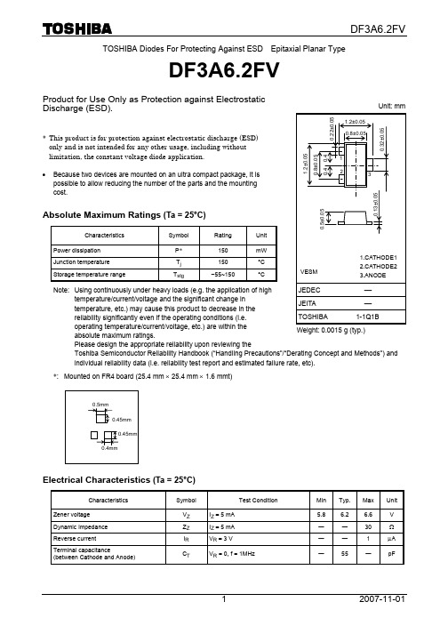
TOSHIBA Diodes For Protecting Against ESD Epitaxial Planar TypeDF3A6.2FVProduct for Use Only as Protection against Electrostatic Discharge (ESD).* This product is for protection against electrostatic discharge (ESD) only and is not intended for any other usage, including without limitation, the constant voltage diode application.• Because two devices are mounted on an ultra compact package, it ispossible to allow reducing the number of the parts and the mounting cost.Absolute Maximum Ratings (Ta = 25°C)Characteristics Symbol RatingUnitPower dissipation P *150 mWJunction temperature T j 150 °C Storage temperature rangeT stg−55~150 °CNote: Using continuously under heavy loads (e.g. the application of hightemperature/current/voltage and the significant change intemperature, etc.) may cause this product to decrease in thereliability significantly even if the operating conditions (i.e.operating temperature/current/voltage, etc.) are within theabsolute maximum ratings.Please design the appropriate reliability upon reviewing theToshiba Semiconductor Reliability Handbook (“Handling Precautions”/“Derating Concept and Methods”) and individual reliability data (i.e. reliability test report and estimated failure rate, etc). *: Mounted on FR4 board (25.4 mm × 25.4 mm × 1.6 mmt)Electrical Characteristics (Ta = 25°C)Characteristics Symbol Test Condition Min Typ. Max UnitZener voltage V Z I Z = 5 mA 5.8 6.26.6VDynamic impedance Z Z I Z = 5 mA ― ― 30 Ω Reverse currentI R V R = 3 V ―― 1 μATerminal capacitance(between Cathode and Anode)C TV R = 0, f = 1MHz― 55 ― pFUnit: mmWeight: 0.0015 g (typ.)Guaranteed Level of ESD ImmunityTest Condition ESD Immunity LevelIEC61000-4-2 (Contact discharge)± 30kVJudgment contents: No element destructionMarking Equivalent Circuit (top view)6.2RESTRICTIONS ON PRODUCT USE20070701-EN •The information contained herein is subject to change without notice.•TOSHIBA is continually working to improve the quality and reliability of its products. Nevertheless, semiconductor devices in general can malfunction or fail due to their inherent electrical sensitivity and vulnerability to physical stress. It is the responsibility of the buyer, when utilizing TOSHIBA products, to comply with the standards of safety in making a safe design for the entire system, and to avoid situations in which a malfunction or failure of such TOSHIBA products could cause loss of human life, bodily injury or damage to property.In developing your designs, please ensure that TOSHIBA products are used within specified operating ranges as set forth in the most recent TOSHIBA products specifications. Also, please keep in mind the precautions and conditions set forth in the “Handling Guide for Semiconductor Devices,” or “TOSHIBA Semiconductor Reliability Handbook” etc.• The TOSHIBA products listed in this document are intended for usage in general electronics applications (computer, personal equipment, office equipment, measuring equipment, industrial robotics, domestic appliances, etc.).These TOSHIBA products are neither intended nor warranted for usage in equipment that requires extraordinarily high quality and/or reliability or a malfunction or failure of which may cause loss of human life or bodily injury (“Unintended Usage”). Unintended Usage include atomic energy control instruments, airplane or spaceship instruments, transportation instruments, traffic signal instruments, combustion control instruments, medical instruments, all types of safety devices, etc.. Unintended Usage of TOSHIBA products listed in his document shall be made at the customer’s own risk.•The products described in this document shall not be used or embedded to any downstream products of which manufacture, use and/or sale are prohibited under any applicable laws and regulations.• Please contact your sales representative for product-by-product details in this document regarding RoHS compatibility. Please use these products in this document in compliance with all applicable laws and regulations that regulate the inclusion or use of controlled substances. Toshiba assumes no liability for damage or losses occurring as a result of noncompliance with applicable laws and regulations.。
FQA8N80C中文资料

Notes:1. Repetitive Rating : Pulse width limited by maximum junction temperature2. L = 22.6mH, I AS = 8.4A, V DD = 50V, R G = 25 Ω, Starting T J = 25°C3. I SD ≤ 8.4A, di/dt ≤ 200A/µs, V DD ≤ BV DSS, Starting T J = 25°C4. Pulse Test : Pulse width ≤ 300µs, Duty cycle ≤ 2%5. Essentially independent of operating temperature∆BV DSS / ∆T J Breakdown Voltage Temperature CoefficientI D = 250 µA, Referenced to 25°C -- 1.02--V/°C I DSS Zero Gate Voltage Drain Current V DS = 800 V, V GS = 0 V ----10µA V DS = 640 V, T C = 125°C ----100µA I GSSF Gate-Body Leakage Current, Forward V GS = 30 V, V DS = 0 V ----100nA I GSSRGate-Body Leakage Current, ReverseV GS = -30 V, V DS = 0 V-----100nAOn CharacteristicsV GS(th)Gate Threshold Voltage V DS = V GS , I D = 250 µA 3.0-- 5.0V R DS(on)Static Drain-Source On-ResistanceV GS = 10 V, I D = 4.2 A -- 1.29 1.55Ωg FSForward TransconductanceV DS = 50 V, I D = 4.2 A (Note 4)-- 5.7--SDynamic CharacteristicsC iss Input Capacitance V DS = 25 V, V GS = 0 V, f = 1.0 MHz--15802050pF C oss Output Capacitance--135175pF C rssReverse Transfer Capacitance--1317pFSwitching Characteristicst d(on)Turn-On Delay Time V DD = 400 V, I D = 8.0 A,R G = 25 Ω(Note 4, 5)--4090ns t r Turn-On Rise Time --110230ns t d(off)Turn-Off Delay Time --65140ns t f Turn-Off Fall Time --70150ns Q g Total Gate Charge V DS = 640 V, I D = 8.0 A,V GS = 10 V(Note 4, 5)--3545nC Q gs Gate-Source Charge --10--nC Q gdGate-Drain Charge--14--nCDrain-Source Diode Characteristics and Maximum RatingsI S Maximum Continuous Drain-Source Diode Forward Current ----8.4A I SM Maximum Pulsed Drain-Source Diode Forward Current----33.6A V SD Drain-Source Diode Forward Voltage V GS = 0 V, I S = 8.4 A ---- 1.4V t rr Reverse Recovery Time V GS = 0 V, I S = 8.4 A,dI F / dt = 100 A/µs (Note 4)--690--ns Q rrReverse Recovery Charge--8.2--µCDISCLAIMERFAIRCHILD SEMICONDUCTOR RESERVES THE RIGHT TO MAKE CHANGES WITHOUT FURTHER NOTICE TO ANY PRODUCTS HEREIN TO IMPROVE RELIABILITY, FUNCTION OR DESIGN. FAIRCHILD DOES NOT ASSUME ANY LIABILITY ARISING OUT OF THE APPLICATION OR USE OF ANY PRODUCT OR CIRCUIT DESCRIBED HEREIN;NEITHER DOES IT CONVEY ANY LICENSE UNDER ITS PATENT RIGHTS, NOR THE RIGHTS OF OTHERS.LIFE SUPPORT POLICYFAIRCHILD’S PRODUCTS ARE NOT AUTHORIZED FOR USE AS CRITICAL COMPONENTS IN LIFE SUPPORT DEVICES OR SYSTEMS WITHOUT THE EXPRESS WRITTEN APPROVAL OF FAIRCHILD SEMICONDUCTOR CORPORATION.As used herein:1. Life support devices or systems are devices or systems which, (a) are intended for surgical implant into the body,or (b) support or sustain life, or (c) whose failure to perform when properly used in accordance with instructions for use provided in the labeling, can be reasonably expected to result in significant injury to the user.2. A critical component is any component of a life support device or system whose failure to perform can be reasonably expected to cause the failure of the life support device or system, or to affect its safety or effectiveness.PRODUCT STATUS DEFINITIONS Definition of TermsDatasheet Identification Product Status DefinitionAdvance InformationFormative or In Design This datasheet contains the design specifications for product development. Specifications may change in any manner without notice.PreliminaryFirst ProductionThis datasheet contains preliminary data, andsupplementary data will be published at a later date.Fairchild Semiconductor reserves the right to make changes at any time without notice in order to improve design.No Identification Needed Full ProductionThis datasheet contains final specifications. Fairchild Semiconductor reserves the right to make changes at any time without notice in order to improve design.Obsolete Not In ProductionThis datasheet contains specifications on a product that has been discontinued by Fairchild semiconductor.The datasheet is printed for reference information only.TRADEMARKSThe following are registered and unregistered trademarks Fairchild Semiconductor owns or is authorized to use and is not intended to be an exhaustive list of all such trademarks.FACT™FACT Quiet series™FAST ®FASTr™FRFET™GlobalOptoisolator™GTO™HiSeC™I 2C™ImpliedDisconnect™ISOPLANAR™LittleFET™MicroFET™MicroPak™MICROWIRE™MSX™MSXPro™OCX™OCXPro™OPTOLOGIC ®OPTOPLANAR™PACMAN™POP™Power247™PowerTrench ®QFET™QS™QT Optoelectronics™Quiet Series™RapidConfigure™RapidConnect™SILENT SWITCHER ®SMART START™SPM™Stealth™SuperSOT™-3SuperSOT™-6SuperSOT™-8SyncFET™TinyLogic ®TruTranslation™UHC™UltraFET ®VCX™ACEx™ActiveArray™Bottomless™CoolFET™CROSSVOLT ™DOME™EcoSPARK™E 2CMOS™EnSigna™Across the board. Around the world.™The Power Franchise™Programmable Active Droop™。
MSMA082资料
(4.803) (3.819) (2.717)
Note: Dimensions reflect incremental type motor. For absolute type motor dimensions, refer to the motor specification.
MFMCB«««0GET 30 - 750W (add'l brake cable)
MFMCA«««2FCT 1.2 - 5.0kW
MFMCA«««3FCT 3.0 - 5.0kW
MSMA _ _ _ A1 _ 2500p/r incremental MSMA _ _ _ C1 _ 17bit absolute for 30 - 750W
battery backup
Specifications
A
Round shaft
B
Round shaft, brake
C
Round shaft, oil seal
D Round shaft, brake & oil seal
E
Key shaft
F
Key shaft, brake
G
Key shaft, oil seal
For customer supplied cables. See the Minas A Series Accessories section
Available for absolute encoder. See the Minas A Series Accessories section
TABLE OF CONTENTS
DC24V
Optional Brake Cable MFMCA«««0EET MFMCB«««0GET MFMCA«««2FCT MFMCA«««3FCT
tps7a8300
1 特性
3 说明
•1 超低压降: 2A 时的最大值为 125mV • 输出电压噪声:6µVRMS • 电源纹波抑制:
– 在 1MHz 时为 40dB • 输入电压范围:
– 无偏置:1.4V 至 6.5V – 有偏置:1.1V 至 6.5V • 两个输出电压模式: – ANY-OUT™ 版本(借助印刷电路板 (PCB) 布
7.4 Device Functional Modes........................................ 24 8 Application and Implementation ........................ 25
8.1 Application Information............................................ 25 8.2 Typical Application .................................................. 29 8.3 Do's and Don'ts ....................................................... 31 9 Power-Supply Recommendations...................... 31 10 Layout................................................................... 32 10.1 Layout Guidelines ................................................. 32 10.2 Layout Example .................................................... 32 11 器件和文档支持 ..................................................... 33 11.1 器件支持................................................................ 33 11.2 文档支持................................................................ 33 11.3 Trademarks ........................................................... 33 11.4 Electrostatic Discharge Caution ............................ 33 11.5 术语表 ................................................................... 33 12 机械封装和可订购信息 .......................................... 34
FAIRCHILD FQPF3N80 数据手册

现货库存、技术资料、百科信息、热点资讯,精彩尽在鼎好!F Q P F 3N 80FQPF3N80800V N-Channel MOSFETGeneral DescriptionThese N-Channel enhancement mode power field effect transistors are produced using Fairchild’s proprietary,planar stripe, DMOS technology.This advanced technology has been especially tailored to minimize on-state resistance, provide superior switching performance, and withstand high energy pulse in the avalanche and commutation mode. These devices are well suited for high efficiency switch mode power supply.TO-220FG SDFQPF3N80(Note 4)(Note 4, 5)(Note 4, 5) (Note 4)Electrical Characteristics T C= 25°C unless otherwise notedNotes:1. Repetitive Rating : Pulse width limited by maximum junction temperature2. L = 185mH, I AS = 1.8A, V DD = 50V, R G = 25 Ω, Starting T J = 25°C3. I SD ≤ 3.0A, di/dt ≤ 200A/µs, V DD ≤ BV DSS, Starting T J = 25°C4. Pulse Test : Pulse width ≤300µs, Duty cycle ≤2%5. Essentially independent of operating temperatureSymbol Parameter Test Conditions Min Typ Max UnitsOff CharacteristicsBV DSS Drain-Source Breakdown Voltage V GS = 0 V, I D = 250 µA800----V ∆BV DSS / ∆T J Breakdown Voltage Temperature CoefficientI D = 250 µA, Referenced to 25°C --0.9--V/°C I DSS Zero Gate Voltage Drain Current V DS = 800 V, V GS = 0 V ----10µA V DS = 640 V, T C = 125°C ----100µA I GSSF Gate-Body Leakage Current, Forward V GS = 30 V, V DS = 0 V ----100nA I GSSRGate-Body Leakage Current, ReverseV GS = -30 V, V DS = 0 V-----100nAOn CharacteristicsV GS(th)Gate Threshold Voltage V DS = V GS , I D = 250 µA3.0-- 5.0V R DS(on)Static Drain-Source On-ResistanceV GS = 10 V, I D = 0.9 A -- 3.8 5.0Ωg FSForward TransconductanceV DS = 50 V, I D = 0.9 A -- 2.3--SDynamic CharacteristicsC iss Input Capacitance V DS = 25 V, V GS = 0 V, f = 1.0 MHz--530690pF C oss Output Capacitance--5775pF C rssReverse Transfer Capacitance--7.09.0pFSwitching Characteristicst d(on)Turn-On Delay Time V DD = 400 V, I D = 3.0 A,R G = 25 Ω--1540ns t r Turn-On Rise Time --4090ns t d(off)Turn-Off Delay Time --3070ns t f Turn-Off Fall Time --3070ns Q g Total Gate Charge V DS = 640 V, I D = 3.0 A,V GS = 10 V--1519nC Q gs Gate-Source Charge -- 3.5--nC Q gdGate-Drain Charge--7.7--nCDrain-Source Diode Characteristics and Maximum RatingsI S Maximum Continuous Drain-Source Diode Forward Current ---- 1.8A I SM Maximum Pulsed Drain-Source Diode Forward Current----7.2A V SD Drain-Source Diode Forward Voltage V GS = 0 V, I S = 1.8 A ---- 1.4V t rr Reverse Recovery Time V GS = 0 V, I S = 3.0 A,dI F / dt = 100 A/µs--530--ns Q rrReverse Recovery Charge-- 2.8--µCF Q P F 3N 80FQPF3N80F Q P F 3N 80FQPF3N80F Q P F 3N 80TRADEMARKSThe following are registered and unregistered trademarks Fairchild Semiconductor owns or is authorized to use and is not intended to be an exhaustive list of all such trademarks.ACEx™Bottomless™CoolFET™CROSSVOLT™DOME™E2CMOS™EnSigna™FACT™FACT Quiet Series™FAST®FASTr™GlobalOptoisolator™GTO™HiSeC™ISOPLANAR™MICROWIRE™OPTOLOGIC™OPTOPLANAR™POP™PowerTrench®QFET™QS™QT Optoelectronics™Quiet Series™SuperSOT™-3SuperSOT™-6SuperSOT™-8SyncFET™TinyLogic™UHC™DISCLAIMERFAIRCHILD SEMICONDUCTOR RESERVES THE RIGHT TO MAKE CHANGES WITHOUT FURTHER NOTICE TO ANY PRODUCTS HEREIN TO IMPROVE RELIABILITY, FUNCTION OR DESIGN. FAIRCHILD DOES NOT ASSUME ANY LIABILITY ARISING OUT OF THE APPLICATION OR USE OF ANY PRODUCT OR CIRCUIT DESCRIBED HEREIN; NEITHER DOES IT CONVEY ANY LICENSE UNDER ITS PATENT RIGHTS, NOR THE RIGHTS OF OTHERS.LIFE SUPPORT POLICYFAIRCHILD’S PRODUCTS ARE NOT AUTHORIZED FOR USE AS CRITICAL COMPONENTS IN LIFE SUPPORT DEVICES OR SYSTEMS WITHOUT THE EXPRESS WRITTEN APPROVAL OF FAIRCHILD SEMICONDUCTOR INTERNATIONAL.As used herein:1. Life support devices or systems are devices or systems which, (a) are intended for surgical implant into the body, or (b) support or sustain life, or (c) whose failure to perform when properly used in accordance with instructions for use provided in the labeling, can be reasonably expected to result in significant injury to the user.2. A critical component is any component of a life support device or system whose failure to perform can be reasonably expected to cause the failure of the life support device or system, or to affect its safety or effectiveness.PRODUCT STATUS DEFINITIONSDefinition of TermsDatasheet Identification Product Status DefinitionAdvance Information Formative or InDesign This datasheet contains the design specifications for product development. Specifications may change in any manner without notice.Preliminary First Production This datasheet contains preliminary data, andsupplementary data will be published at a later date.Fairchild Semiconductor reserves the right to makechanges at any time without notice in order to improvedesign.No Identification Needed Full Production This datasheet contains final specifications. FairchildSemiconductor reserves the right to make changes atany time without notice in order to improve design. Obsolete Not In Production This datasheet contains specifications on a productthat has been discontinued by Fairchild semiconductor.The datasheet is printed for reference information only.VCX™。
样本册-滤波器140507
插入损耗 插入耗损是在标准50Ω系统条件下测定的
FLAC32-3A
FLAC32-6A
共模
差模
FLAC12B-3WE
FLAC12B-6WE
外形尺寸 单位(mm) FLAC32-3A FLAC32-6A FLAC12B-3WE FLAC12B-6WE
电路图原理图
10
单相D系列滤波器
产品特点 良好的共模、差模抑制性,能有效的抑制线-线、 线-地之间的电磁干扰。 灵活的安装方式 满足UL & ENEC的认证
声明 本书中所列技术参数仅供参考,技术参数如有变化恕不另行通知,请以实物及产品《技术规格书》为准,详情请联系
中石公司。
5
JONES 单相电源滤波器
单相A系列滤波器
产品特点 良好的共模、差模抑制性,能有效的抑制线-线、 线-地之间的电磁干扰。 低泄漏电流 灵活的安装方式 满足UL & ENEC的认证
6A
10A
1768VDC/1min
115/250
<0.5mA@250VAC, (line/line)
20A
50/60 Hz
VAC
50Hz
2000VAC/1min
30A
(lines/case)
6A
FLHDB3H-10LL
10A
FLHDM3H-10LL
10A
气候类别 25/85/21
插入损耗 插入耗损是在标准50Ω系统条件下测定的
d1B00
50
0
0.01
0.10
1.00
10
0
100MHz
0.01
0.10
1.00
10
100MHz
FLHD01-6A
DF7手册
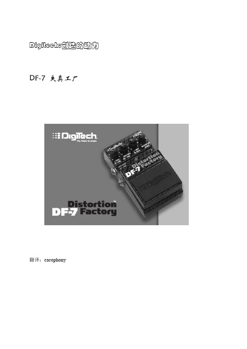
Digitech:创造的动力DF-7 失真工厂翻译:cacophony一致声明:厂商名称:Digitech厂商地址:8760 S. Sandy Parkway Sandy, Utah 84070, USA产品声明:产品名称:DF-7 失真工厂产品选择:全部(需要符合EN60065,EN60742要求的Class II电源适配器或其他同类产品)遵守以下产品制造规格:安全性:IEC60050(1998)电磁兼容性:EN55013(1990) EN55020(1991)辅助信息:本产品还符合如下标准:低压指导 73/23/EEC电磁兼容指导 89/336/EEC 及修正 93/68/EEC工程副总监-MI8760 S. Sandy Parkway Sandy, Utah 84070, USA日期:2004年12月13日欧洲承包商:您所在地的Digitech销售服务部门或Harman Music Group ,8760 S. Sandy Parkway Sandy, Utah 84070, USA电话:(801)566-8800传真:(801)568-7583警告:为了保护您,请阅读以下条款:重要的安全说明1、阅读本说明;2、保存本说明;3、注意所有警告;4、禁止在水边使用本产品;5、只能用干燥布料清洁本产品;6、不要堵塞本产品的任何通风口,按照厂家说明来安装本产品;7、不要将本产品安装在任何形式的热源附近,包括:散热器,热容器,炉,以及其他产生热能的仪器(包括音箱);8、保护电源线不被踩踏或缠绕在插座、方便插座以及与效果器的接口上;9、在雷雨天或长时间放置不用时请拔掉电源;10、户不能自行维修本产品,如有需要请联系有资格的维修人员,当本产品出现任何形式的损坏时都需要进行维修,如电源线或插座损坏,电池液体泄露或本产品内掉入杂物,本产品淋雨或暴露在潮湿空气中,非正常工作,或被摔坏;11、警告:为了降低着火或电击的危险,请勿将本产品暴露在雨中或潮湿空气中;12、注意本产品上的商标,包括后盖,或其他标记及相关信息。
DF08中文资料

Maximum Ratings and Electrical Characteristics
(Ratings at 25oC ambient temperature unless otherwise specified.)
Parameter Maximum repetitive peak reverse voltage Maximum RMS voltage Maximum DC blocking voltage Maximum average forward output rectified current at TA=40oC Peak forward surge current single half sine-wave superimposed on rated load (JEDEC Method) Rating for fusing (t < 8.3ms) Max. instantaneous forward voltage drop per leg at 1.0A Maximum DC reverse current at rated DC blocking voltage per leg TA=25oC TA=125oC
D F 06 600 420 600
D F 08 800 560 800
D F 10 1000 700 1000
Units Volts Volts Volts Amp Amps A 2 se c Volts uA pF
o
Typical junction capacitance per leg at 4.0V, 1MHz Typical thermal resistance per leg (Note 1) Operating junction and storage temperature range
LFS系列液体流量开关规格说明书

Page 1Copyright © 2021 Sensata Technologies, Inc. | LFS SERIESPADDLE FLOW SWITCHESSPECIFICATIONSThe LFS range of flow switches are paddle devices that are mounted vertically through a socket or upstand process connection.Electrical connections are made within the housing, which has a screw on sealed lid and cable gland.A choice of paddle sizes is supplied with each switch and selection can be made with reference to the chart below.TechnicalElectricalFeatures• Stainless steel SS304 paddle• 3/4”BSP or 1”NPT mounting plug thread• IP65 Aluminium alloy housing or DIN 43650 connection • Use for flow detection in pipes from 1” bore to 3” bore• Maximum operating pressure 20 barHousing materialAluminium Alloy Paddle material 304grade SS Temperature range See chart below Maximum pressure 20 bar Set point tolerance ±25 %Pressure drop0.2 barConnection in housing or byDIN 43650Mounting thread1”NPT STANDARD PARTSAll ratings are for resistive load only.Page 2CONTACT USCynergy3 Components Ltd.7 Cobham Road,Ferndown Industrial Estate, Wimborne, Dorset,BH21 7PE, United KingdomCopyright © 2021 Sensata Technologies, Inc.Sensata Technologies, Inc. (“Sensata”) data sheets are solely intended to assist designers (“Buyers”) who are developing systems that incorporate Sensata products (also referred to herein as “components”). Buyer understands and agrees that Buyer remains responsible for using its independent analysis, evaluation and judgment in designing Buyer’s systems and products. Sensata data sheets have been created using standard laboratory conditions and engineering practices. Sensata has not conducted any testing other than that specifically described in the published documentation for a particular data sheet. Sensata may make corrections, enhancements, improvements and other changes to its data sheets or components without notice.Buyers are authorized to use Sensata data sheets with the Sensata component(s) identified in each particular data sheet. HOWEVER, NO OTHER LICENSE, EXPRESS OR IMPLIED, BY ESTOPPEL OR OTHERWISE TO ANY OTHER SENSATA INTELLECTUAL PROPERTY RIGHT, AND NO LICENSE TO ANY THIRD PARTY TECHNOLOGY OR INTELLECTUAL PROPERTY RIGHT, IS GRANTED HEREIN. SENSATA DATA SHEETS ARE PROVIDED “AS IS”. SENSATA MAKES NO WARRANTIES OR REPRESENTATIONS WITH REGARD TO THE DATA SHEETS OR USE OF THE DATA SHEETS, EXPRESS, IMPLIED OR STATUTORY, INCLUDING ACCURACY OR COMPLETENESS. SENSATA DISCLAIMS ANY WARRANTY OF TITLE AND ANY IMPLIED WARRANTIES OF MERCHANTABILITY, FITNESS FOR A PARTICULAR PURPOSE, QUIET ENJOYMENT, QUIET POSSESSION, AND NON-INFRINGEMENT OF ANY THIRD PARTY INTELLECTUAL PROPERTY RIGHTS WITH REGARD TO SENSATA DATA SHEETS OR USE THEREOF.All products are sold subject to Sensata’s terms and conditions of sale supplied at SENSATA ASSUMES NO LIABILITY FOR APPLICATIONS ASSISTANCE OR THE DESIGN OF BUYERS’ PRODUCTS. BUYER ACKNOWLEDGES AND AGREES THAT IT IS SOLELY RESPONSIBLE FOR COMPLIANCE WITH ALL LEGAL, REGULATORY AND SAFETY-RELATED REQUIREMENTS CONCERNING ITS PRODUCTS, AND ANY USE OF SENSATA COMPONENTS IN ITS APPLICATIONS, NOTWITHSTANDING ANY APPLICATIONS-RELATED INFORMATION OR SUPPORT THAT MAY BE PROVIDED BY SENSATA.Mailing Address: Sensata Technologies, Inc., 529 Pleasant Street, Attleboro, MA 02703, USA.ISO9001CERTIFIED cynergy3-lfs-v3 Rev: 07/10/21Mechanical DimensionsRepeatability ±5% Connection in housing or by DIN 43650Contact Form SPDT Electrical Specification 180Model No.LFS-02/H Model No.LFS-03/H Model No.LFS-04/HModel No.LFS-01/H Made in the UK。
ADC0808_07资料
VIN=0
ICC
Supply Currentபைடு நூலகம்
DATA OUTPUTS AND EOC (INTERRUPT)
fCLK=640 kHz
VOUT(1)
VOUT(0) VOUT(0) IOUT
Logical “1” Output Voltage
Logical “0” Output Voltage Logical “0” Output Voltage EOC TRI-STATE Output Current
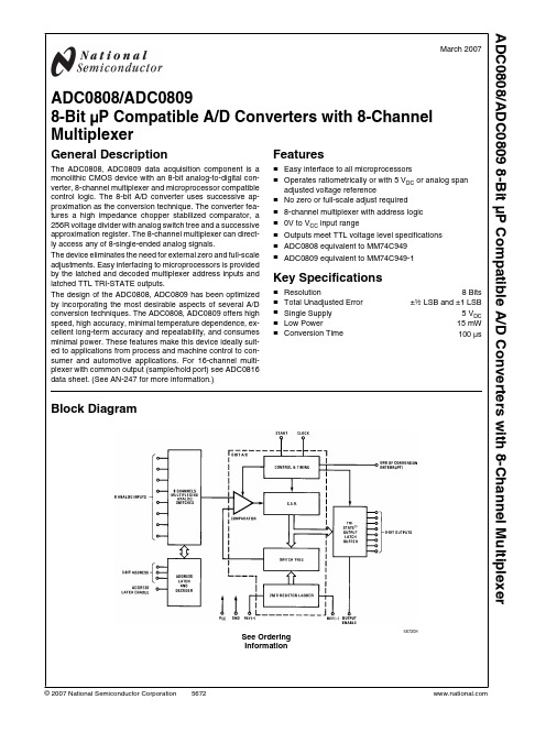
ADC0808/ADC0809 8-Bit μP Compatible A/D Converters with 8-Channel Multiplexer
元器件交易网
March 2007
ADC0808/ADC0809
8-Bit μP Compatible A/D Converters with 8-Channel Multiplexer
See Ordering Information
© 2007 National Semiconductor Corporation 5672
567201
ADC0808/ADC0809
元器件交易网
Connection Diagrams
Dual-In-Line Package
Symbol
Parameter
Conditions
Min
Typ
Max
Units
ANALOG MULTIPLEXER
IOFF(+)
OFF Channel Leakage Current
IOFF(−)
OFF Channel Leakage Current
ACF焊荐_8
형식 FV2300-DOS/RP64F SGMAH-08AAA-21 SGMAH-02AAA-21 EE-SX671 350P5M15 GLS-1 BV-RB10TPZ GP2600-TC11 TPM-233-02 GLS-1 CDQ2-L-80D-P6030-XC10 EE-SX671 T110AR1U1 KBM11-25-16C KBM11-25-20C HL-Φ14x520(특주 품 :4G8VMX23-01) HL-Φ14x770(특주 품 :94534870-20) HT-20-Φ1.6x 80L(F-204) (K0840030-02) 5561(아 연 도금 )(K0840027-01) 6870(아 연 도금 )(K0841257-01) LS250280AL2-002P63(3G8V046-01) MTA4SL-450 MSC-2-A8 FCBN-6K CDQS-B-12-15D-M9B FS-V11 FU-85 EE-SX672A MXU-6-25-M9B CDRB1-BW-10-90S-T99L RH905-FS.OT2 SGMAH-A5AAA-21 E32-T16P E32-T22L E32-D32 E3X-DA11-N MXQ-8L-10-M9BL MXQ-8-20-M9BL MXH-6-5-M9BLS 148-824MHS6-13L
6 E 8 V M B 1 8
8
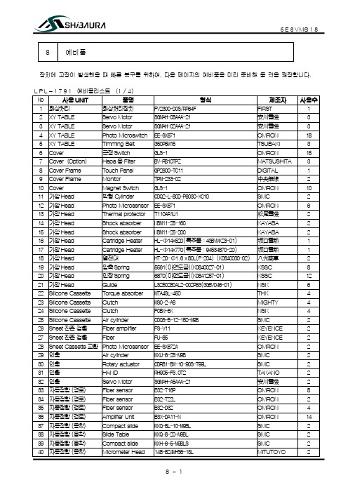
예비품
장치에 고장이 발생했을 때 빠른 복구를 위하여, 다음 페이지의 예비품을 미리 준비해 둘 것을 권장합니다. L P L - 1 7 9 1 예비품리스트 ( 1 / 4 ) No 사용 UNIT 품명 1 화상 처 리 화상 처 리장 치 2 XY TABLE Servo Motor 3 XY TABLE Servo Motor 4 XY TABLE Photo Microswitch 5 XY TABLE Timming Belt 6 Cover 근접Switch 7 Cover(Option) Hepa 용 Filter 8 Cover Frame Touch Panel 9 Cover Frame Monitor 10 Cover Magnet Switch 11 가압Head 박형 Cylinder 12 가압Head Photo Microsensor 13 가압Head Thermal protector 14 가압Head Shock absorber 15 가압Head Shock absorber 16 가압Head Cartridge Heater 17 가압Head Cartridge Heater 18 가압Head 열전 대 19 가압Head 압축Spring 20 가압Head 인장Spring 21 가압Head Guide 22 Silicone Cassette Torque absorber 23 Silicone Cassette Clutch 24 Silicone Cassette Clutch 25 Silicone Cassette Air cylinder 26 Sheet 잔 존검 출 Fiber amplifier 27 Sheet 잔 존검 출 Fiber 28 Sheet Cassette 교 환 Photo Microsensor 29 인출 Air cylinder 30 인출 Rotary actuator 31 인출 HAND 32 인출 Servo Motor 33 자동 접 합 (경로 ) Fiber sensor 34 자동 접 합 (경로 ) Fiber sensor 35 자동 접 합 (경로 ) Fiber sensor 36 자동 접 합 (경로 ) Amplifier Unit 37 자동 접 합 (용착 ) Compact slide 38 자동 접 합 (용착 ) Slide Table 39 자동 접 합 (용착 ) Compact slide 40 자동 접 합 (용착 ) Micrometer Head
DF无线数据收发模块
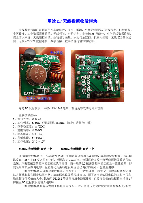
用途DF无线数据收发模块无线数据传输广泛地运用在车辆监控、遥控、遥测、小型无线网络、无线抄表、门禁系统、小区传呼、工业数据采集系统、无线标签、身份识别、非接触RF智能卡、小型无线数据终端、安全防火系统、无线遥控系统、生物信号采集、水文气象监控、机器人控制、无线232数据通信、无线485/422数据通信、数字音频、数字图像传输等领域中。
这是DF发射模块,体积:19x19x8毫米,右边是等效的电路原理图主要技术指标:1。
通讯方式:调幅AM2。
工作频率:315MHZ (可以提供433MHZ,购货时请特别注明)3。
频率稳定度:±75KHZ4。
发射功率:≤500MW5。
静态电流:≤0.1UA6。
发射电流:3~50MA7。
工作电压:DC 3~12V315MHZ发射模块 8元一个433MHZ发射模块 8元一个DF数据发射模块的工作频率为315M,采用声表谐振器SAW稳频,频率稳定度极高,当环境温度在-25~+85度之间变化时,频飘仅为3ppm/度。
特别适合多发一收无线遥控及数据传输系统。
声表谐振器的频率稳定度仅次于晶体,而一般的LC振荡器频率稳定度及一致性较差,即使采用高品质微调电容,温差变化及振动也很难保证已调好的频点不会发生偏移。
DF发射模块未设编码集成电路,而增加了一只数据调制三极管Q1,这种结构使得它可以方便地和其它固定编码电路、滚动码电路及单片机接口,而不必考虑编码电路的工作电压和输出幅度信号值的大小。
比如用PT2262等编码集成电路配接时,直接将它们的数据输出端第17脚接至DF数据模块的输入端即可。
DF数据模块具有较宽的工作电压范围3~12V,当电压变化时发射频率基本不变,和发射模块配套的接收模块无需任何调整就能稳定地接收。
当发射电压为3V时,空旷地传输距离约20~50米,发射功率较小,当电压5V时约100~200米,当电压9V时约300~500米,当发射电压为12V时,为最佳工作电压,具有较好的发射效果,发射电流约60毫安,空旷地传输距离700~800米,发射功率约500毫瓦。
ul758中文版
ul758中文版电器布线电线电缆及其试验方法Standard for Appliance Wiring MaterialUL 758/2000上海电缆研究所电线电缆信息中心37电容和相对电容率试验(潮湿场所缴AWM) (83)37A稳定因数(潮湿场所缴AWM) (83)燃烧性能试验 (84)38用途等级I的水平燃烧试验 (84)39用途等级II的垂直燃烧试验 (84)40 VW-1燃烧试验 (84)41 FT1燃烧试验 (84)42 FT2燃烧试验 (84)制造和生产试验 (85)43导体连续性试验 (85)44 火花试验 (86)标志 (88)45AWM的表面标志 (88)46标牌,线盘或纸箱上的标志 (88)47多重标志 (89)导论1范围1.1本标准适用于电器布线线缆(AWM),这些布线线缆可以是单芯电线、多芯电缆、光纤或用作多芯电缆构件的绝缘线芯和光纤元件。
1.2适用于本标准的电器布线线缆(AWM),仅用作工厂安装布线,它们可以是电器或其它设备外壳内的布线(内部布线),或电器之间的互连线(外部布线),或作为多芯电缆的构件用于进一步加工。
1.3本标准不适用于目前由美国国家电气规程(NEC)NFPA70纳入的任何电线、电缆或软线,如果它们在拟用于的最终产品的安装说明范围外不打算按NEC规程敷设在建筑或结构中的话。
1.4适用于本标准的电器布线线缆(AWM),最低工作温度为60℃(140°F)干燥环境,最低额定电压为30V。
导体规格从50AWG~2000kcmil不等。
完全由光纤元件组成的电器布线线缆或由导线与光纤元件复合组成的电器布线线缆,也适用于本标准。
1.5本标准不涉及任何光纤元件或光纤元件组的光学性能。
1.6除了上述结构的电线电缆外,本标准还建成立了评件特殊结构电线电缆的导则,这些电线电缆由于拟用于的最终产品的性质不需要满足通用电器布线线缆的全部要求。
1.7电器布线线缆(AWM)的最终验收,取决于它在符合适用标准的完整设备中的使用。
风云卫星数据和产品应用手册
风云卫星数据和产品应用手册第1章概述1.1 FY-3A卫星概况风云三号A气象卫星(简称FY-3A)是我国的第二代太阳同步极轨气象卫星。
风云三号气象卫星将实现全球、全天候、多光谱、三维、定量对地观测。
风云三号星发射总质量为2450kg,发射尺寸:4.38m×2m×2m,卫星长期功耗1130W。
卫星本体由服务舱、推进舱与有效载荷舱组成。
服务舱采用中心承力筒和隔板结构,主要安装电源、测控、数管及姿轨控分系统的部件和设备、推进舱采用中心承筒和隔板结构,主要安装推进系统设备以及蓄电池组和放电调节器。
有效载荷舱隔板和构架结构,主要安装探测仪器的探测头部,舱内主要安装探测仪器的电子设备等。
风云三号A卫星有十一台遥感探测仪器。
遥感数据通过两个实时传输信道(HRPT和MPT)和一个延时传输信道(DPT)进行传输。
风云三号A卫星设计寿命为3年。
1.2 主要技术指标1.2.1 卫星轨道⑴轨道类型:近极地太阳同步轨道⑵轨道标称高度:831公里⑶轨道倾角:98.81°⑷入轨精度:半长轴偏差: |Δa|≤5公里轨道倾角偏差:|Δi|≤0.1°轨道偏心率≤0.003⑸标称轨道回归周期为5.79天⑹轨道保持偏心率:≤0.00013⑺交点地方时漂移:2年小于15分钟⑻卫星发射窗口:降交点地方时10:051.2.2 卫星姿态⑴姿态稳定方式:三轴稳定⑵三轴指向精度:≤0.3°⑶三轴测量精度:≤0.05°⑷三轴姿态稳定度:≤4×10⁻³ °/s1.2.3 太阳帆板对日定向跟踪1.2.4 星上记时⑴记时方式:J2000日计数和日毫秒计数⑵记时单位:1毫秒⑶时间精度(星地总精度):小于20毫秒1.2.5 遥感探测仪器性能指标1.2.5.1 可见光红外扫描辐射计(VIRR)(1)通道数、各通道波段范围、灵敏度见表1-1。
(2)空间分辨率:星下点分辨率1.1Km(3)扫描范围:±55.4°(4)扫描器转速:6线/秒(5)每条扫描线采样点数:2048(6)MTF≥0.3(7)通道配准:飞行方向/扫描方向星下点配准精度<0.5个像元(8)扫描抖动:<0.8个IFOV(9)通道信号衰减:<15%/2年(10)量化等级:10比特(11)定标精度:可见光和近红外通道:CH1、2、7、8、9 7%(反射率)CH6、10 10%(反射率)红外通道:1k(270k)。
- 1、下载文档前请自行甄别文档内容的完整性,平台不提供额外的编辑、内容补充、找答案等附加服务。
- 2、"仅部分预览"的文档,不可在线预览部分如存在完整性等问题,可反馈申请退款(可完整预览的文档不适用该条件!)。
- 3、如文档侵犯您的权益,请联系客服反馈,我们会尽快为您处理(人工客服工作时间:9:00-18:30)。
• Low terminal capacitance : CT = 5.0 pF (typ.)
Electrical Characteristics (Ta = 25°C)
Characteristics
Zener voltage Dynamic impedance Knee dynamic impedance Reverse current Terminal capacitance (between Cathode and Anode)
Symbol
VZ ZZ ZZK IR
CT
Test Condition
IZ = 5 mA IZ = 5 mA IZ = 0.5 mA VR = 5 V
VR = 0 V, f = 1 MHz
Min Typ. Max Unit
7.8 8.2 8.6
V
⎯
⎯
60
Ω
⎯
⎯
100
Ω
⎯
⎯
0.5
μA
⎯
5.0
⎯
pF
Guaranteed Level of ESD Immunity
• Please contact your sales representative for product-by-product details in this document regarding RoHS compatibility. Please use these products in this document in compliance with all applicable laws and regulations that regulate the inclusion or use of controlled substances. Toshiba assumes no liability for damage or losses occurring as a result of noncompliance with applicable laws and regulations.
3
2007-11-01
元器件交易网
DF3A8.2LFU
RESTRICTIONS ON PRODUCT USE
20070701-EN
• The information contained herein is subject to change without notice.
• TOSHIBA is continually working to improve the quality and reliability of its products. Nevertheless, semiconductor devices in general can malfunction or fail due to their inherent electrical sensitivity and vulnerability to physical stress. It is the responsibility of the buyer, when utilizing TOSHIBA products, to comply with the standards of safety in making a safe design for the entire system, and to avoid situations in which a malfunction or failure of such TOSHIBA products could cause loss of human life, bodily injury or damage to property. In developing your designs, please ensure that TOSHIBA products are used within specified operating ranges as set forth in the most recent TOSHIBA products specifications. Also, please keep in mind the precautions and conditions set forth in the “Handling Guide for Semiconductor Devices,” or “TOSHIBA Semiconductor Reliability Handbook” etc.
°C
Note: Using contg. the application of high
JEDEC
―
temperature/current/voltage and the significant change in
temperature, etc.) may cause this product to decrease in the
Absolute Maximum Ratings (Ta = 25°C)
Characteristics
Symbol
Rating
Unit
Power dissipation
P
100
mW
Junction temperature Storage temperature range
Tj
125
°C
Tstg
−55 ~ 125
Test Condition
ESD Immunity Level
IEC61000-4-2 (Contact discharge)
± 6kV
Criterion: No damage to device elements
Marking
FU
Equivalent Circuit
(top view)
1
2007-11-01
• The products described in this document shall not be used or embedded to any downstream products of which manufacture, use and/or sale are prohibited under any applicable laws and regulations.
JEITA
―
reliability significantly even if the operating conditions (i.e. operating temperature/current/voltage, etc.) are within the
TOSHIBA
1-2P1A
absolute maximum ratings. Please design the appropriate reliability upon reviewing the
DF3A8.2LFU
IF – VF
100
10
1
0.5 0.6 0.7
0.8 0.9
1
1.1 1.2
Forward voltage VF (V)
Total capacitance CT (pF)
1 0 1 2 3 4 5 6 7 8 9 10
Reverse voltage VR (V)
2
2007-11-01
元器件交易网 DF3A8.2LFU
TOSHIBA Diodes for Protecting against ESD Epitaxial Planar Type
DF3A8.2LFU
Product for Use Only as Protection against Electrostatic Discharge (ESD)
元器件交易网
Zener current IZ (A)
100 m 10 m
IZ – VZ
1m 100 μ
10 μ
1μ 5 6 7 8 9 10 11 12 13 14 15
Zener voltage VZ (V)
CT – VR
10
Ta = 25°C f = 1 MHz
Forward current IF (mA)
• The TOSHIBA products listed in this document are intended for usage in general electronics applications (computer, personal equipment, office equipment, measuring equipment, industrial robotics, domestic appliances, etc.).These TOSHIBA products are neither intended nor warranted for usage in equipment that requires extraordinarily high quality and/or reliability or a malfunction or failure of which may cause loss of human life or bodily injury (“Unintended Usage”). Unintended Usage include atomic energy control instruments, airplane or spaceship instruments, transportation instruments, traffic signal instruments, combustion control instruments, medical instruments, all types of safety devices, etc.. Unintended Usage of TOSHIBA products listed in his document shall be made at the customer’s own risk.
