Resonant Tunneling through Multi-Level and Double Quantum Dots
纳米领域中的电子隧穿方式
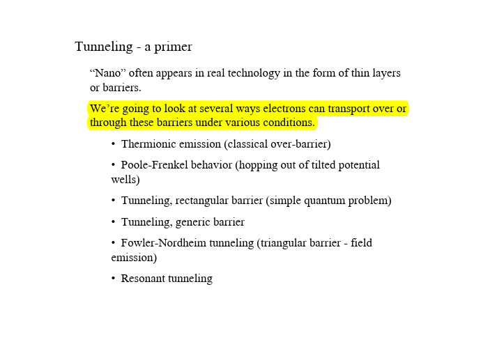
Tunneling -a primer“Nano”often appears in real technology in the form of thin layers or barriers.We’re going to look at several ways electrons can transport over or through these barriers under various conditions.•Thermionic emission (classical over-barrier)•Poole-Frenkel behavior (hopping out of tilted potentialwells)•Tunneling, rectangular barrier (simple quantum problem)•Tunneling, generic barrier•Fowler-Nordheim tunneling (triangular barrier -fieldemission)•Resonant tunnelingThermionic emission: applicationsThermionic emission often governs:•Electron injection into semiconductors from metals.•Emission of electrons from hot materials into vacuum(the filament in every cathode ray tube, ion gauge, etc.)•Partly responsible for emission in thermal fieldemission sources (electron microscopy).Poole-Frenkel behaviorIf hopping rate is activated,]/exp[~0T k U B −σLowering of barrier means]/)4/(exp[~2/103T k F e B πεεσ−→Scaling of conductance with T and F like this is the signature of Poole-Frenkel behavior.Prevalent in organic semiconductors, amorphous Si, etc.Combined picture:Realistic tunneling probabilitiesAs we saw from rectangularbarrier case, tunneling onlyoccurs with significant probabilityat very short length scales (verynarrow barriers).Tunneling is exponentiallysuppressed with barrier width.Factoid: metal-metal tunneling current in vacuum (or air) decays with distance roughly like 1 order of magnitude per Angstrom (!).One of your homework problems: what is the probability ofa Volkswagon Beetle tunneling through a speed bump?Resonant tunnelingAlgebra gets a bit messy….image from FerryResonant tunneling diodeDoes this actually work?GaAs RTD, AlGaAs barriers, a= b= 5 nm. image from FerryA very subtle questionA philosophy question worth pondering, even thoughit’s not directly germane to the course:How long does the tunneling process take?That is, for particles that successfully traverse barrier,how long are they “in”the classically forbidden region?Consider incident Gaussian wavepacket + transmittedGaussian wavepacket.Surprising answer: measuring positions of peaks ofwavepacket, tunneling “velocity”can greatly exceed c!For more information, read Landauer and Martin, RMP66, 217 (1994).To summarize:•Thermionic emission = classical thermal over-barrier•Poole-Frenkel = field-assisted classical thermal hopping•Single-barrier tunneling is straightforward.•Generic barriers: WKB approximation•Fowler-Nordheim = field-assisted tunneling•Double barriers: must account for interference•Result: resonant tunneling diodes w/ NDR•Nontrivial interpretation issues associated with tunneling!Next time:•Scattering matrices•Landauer-Buttiker formalism -conductance as transmission.。
声学超构材料术语

声学超构材料术语1范围本文件规定了包括声子晶体、声超材料等人工微结构的声学超构材料等相关术语的定义。
本文件适用于声学超构材料及其相关领域的活动。
2规范性引用文件下列文件对于本文件的应用是必不可少的。
凡是注日期的引用文件,仅所注日期的版本适用于本文件。
凡是不注日期的引用文件,其最新版本(包括所有的修改单)适用于本文件。
GB/T32005-2015电磁超材料术语GB/T3947-1996声学名词术语3基础定义3.1超构材料metamaterials一种特种复合材料或结构,通过对材料关键物理尺度上进行一定序构设计,使其获得常规材料所不具备的超常物理性能。
3.2声学超构材料acoustic metamaterials具备超常声学特性的一类超构材料3.3声子晶体phononic crystal由两种以上具有不同弹性参数的材料按一定空间序构周期排列的复合人工介质形成的一种声学超构材料。
4分类4.1固体弹性波超构材料solid elastic wave metamaterials用于调控固体中弹性波的声学超构材料。
4.2水声超构材料underwater acoustic metamaterials用于调控水中声波的声学超构材料。
4.3空气声超构材料用于调控空气中声波的声学超构材料。
4.4次声声学超构材料infrasound metamaterials工作频率在20Hz以下的声学超构材料4.5超声声学超构材料ultrasonic metamaterials工作频率在20kHz以上的声学超构材料4.6可听声超构材料audible sound metamaterials工作频率在20Hz-20kHz范围的声学超构材料4.7局域共振型声学超构材料resonant acoustic metamaterials基于局域共振原理的声学超构材料4.8非局域共振型声学超构材料non-resonant acoustic metamaterials 不基于局域共振原理的声学超构材料4.9线性声学超构材料linear metamaterials具有线性动力学效应的声学超构材料4.10非线性声学超构材料nonlinear metamaterials具有非线性动力学效应的声学超构材料4.11各向同性声学超构材料isotropic acoustic metamaterials具有各向同性的声学特性的声学超构材料4.12各向异性声学超构材料anisotropic acoustical metamaterials具有各向异性的声学特性的声学超构材料4.13复合声学超构材料composite acoustic metamaterials与其他材料复合的声学超构材料4.14可重构声学超构材料reconfigurable acoustic metamaterials宏观或微观结构可重构的声学超构材料4.15可编程声学超构材料programmable acoustic metamaterials利用逻辑基元对声场进行程序化调控的声学超构材料4.16微纳声学超构材料micro-scale acoustic metamaterials微观结构的绝对尺度在微米或纳米级的声学超构材料4.17多物理场耦合型超构材料multi-physical coupled metamaterials 声场与其他物理场相互耦合的声学超构材料4.18吸声超构材料sound absorption metamaterials能够有效控制噪声且尺寸小巧的声学超构材料。
英语
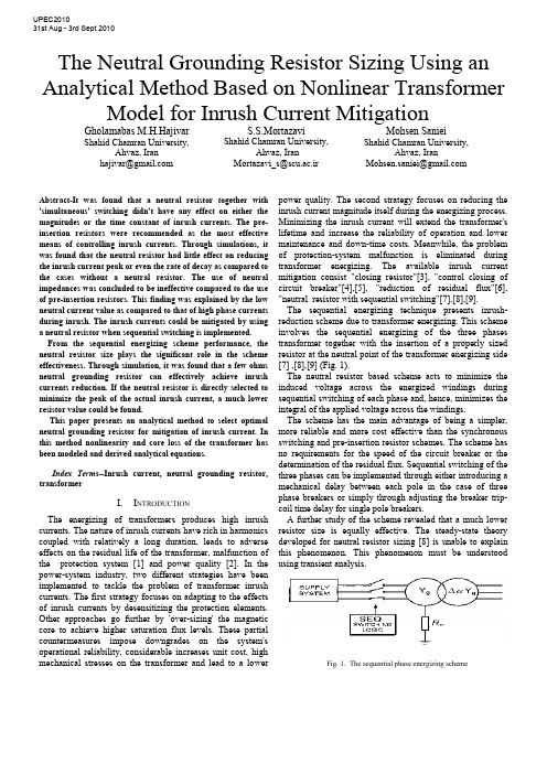
The Neutral Grounding Resistor Sizing Using an Analytical Method Based on Nonlinear Transformer Model for Inrush Current MitigationGholamabas M.H.Hajivar Shahid Chamran University,Ahvaz, Iranhajivar@S.S.MortazaviShahid Chamran University,Ahvaz, IranMortazavi_s@scu.ac.irMohsen SanieiShahid Chamran University,Ahvaz, IranMohsen.saniei@Abstract-It was found that a neutral resistor together with 'simultaneous' switching didn't have any effect on either the magnitudes or the time constant of inrush currents. The pre-insertion resistors were recommended as the most effective means of controlling inrush currents. Through simulations, it was found that the neutral resistor had little effect on reducing the inrush current peak or even the rate of decay as compared to the cases without a neutral resistor. The use of neutral impedances was concluded to be ineffective compared to the use of pre-insertion resistors. This finding was explained by the low neutral current value as compared to that of high phase currents during inrush. The inrush currents could be mitigated by using a neutral resistor when sequential switching is implemented. From the sequential energizing scheme performance, the neutral resistor size plays the significant role in the scheme effectiveness. Through simulation, it was found that a few ohms neutral grounding resistor can effectively achieve inrush currents reduction. If the neutral resistor is directly selected to minimize the peak of the actual inrush current, a much lower resistor value could be found.This paper presents an analytical method to select optimal neutral grounding resistor for mitigation of inrush current. In this method nonlinearity and core loss of the transformer has been modeled and derived analytical equations.Index Terms--Inrush current, neutral grounding resistor, transformerI.I NTRODUCTIONThe energizing of transformers produces high inrush currents. The nature of inrush currents have rich in harmonics coupled with relatively a long duration, leads to adverse effects on the residual life of the transformer, malfunction of the protection system [1] and power quality [2]. In the power-system industry, two different strategies have been implemented to tackle the problem of transformer inrush currents. The first strategy focuses on adapting to the effects of inrush currents by desensitizing the protection elements. Other approaches go further by 'over-sizing' the magnetic core to achieve higher saturation flux levels. These partial countermeasures impose downgrades on the system's operational reliability, considerable increases unit cost, high mechanical stresses on the transformer and lead to a lower power quality. The second strategy focuses on reducing the inrush current magnitude itself during the energizing process. Minimizing the inrush current will extend the transformer's lifetime and increase the reliability of operation and lower maintenance and down-time costs. Meanwhile, the problem of protection-system malfunction is eliminated during transformer energizing. The available inrush current mitigation consist "closing resistor"[3], "control closing of circuit breaker"[4],[5], "reduction of residual flux"[6], "neutral resistor with sequential switching"[7],[8],[9].The sequential energizing technique presents inrush-reduction scheme due to transformer energizing. This scheme involves the sequential energizing of the three phases transformer together with the insertion of a properly sized resistor at the neutral point of the transformer energizing side [7] ,[8],[9] (Fig. 1).The neutral resistor based scheme acts to minimize the induced voltage across the energized windings during sequential switching of each phase and, hence, minimizes the integral of the applied voltage across the windings.The scheme has the main advantage of being a simpler, more reliable and more cost effective than the synchronous switching and pre-insertion resistor schemes. The scheme has no requirements for the speed of the circuit breaker or the determination of the residual flux. Sequential switching of the three phases can be implemented through either introducing a mechanical delay between each pole in the case of three phase breakers or simply through adjusting the breaker trip-coil time delay for single pole breakers.A further study of the scheme revealed that a much lower resistor size is equally effective. The steady-state theory developed for neutral resistor sizing [8] is unable to explain this phenomenon. This phenomenon must be understood using transient analysis.Fig. 1. The sequential phase energizing schemeUPEC201031st Aug - 3rd Sept 2010The rise of neutral voltage is the main limitation of the scheme. Two methods present to control the neutral voltage rise: the use of surge arrestors and saturated reactors connected to the neutral point. The use of surge arresters was found to be more effective in overcoming the neutral voltage rise limitation [9].The main objective of this paper is to derive an analytical relationship between the peak of the inrush current and the size of the resistor. This paper presents a robust analytical study of the transformer energizing phenomenon. The results reveal a good deal of information on inrush currents and the characteristics of the sequential energizing scheme.II. SCHEME PERFORMANCESince the scheme adopts sequential switching, each switching stage can be investigated separately. For first-phase switching, the scheme's performance is straightforward. The neutral resistor is in series with the energized phase and this resistor's effect is similar to a pre-insertion resistor.The second- phase energizing is one of the most difficult to analyze. Fortunately, from simulation studies, it was found that the inrush current due to second-phase energizing is lower than that due to first-phase energizing for the same value of n R [9]. This result is true for the region where the inrush current of the first-phase is decreasing rapidly as n R increases. As a result, when developing a neutral-resistor-sizing criterion, the focus should be directed towards the analysis of the first-phase energizing.III. A NALYSIS OF F IRST -P HASE E NERGIZING The following analysis focuses on deriving an inrush current waveform expression covering both the unsaturatedand saturated modes of operation respectively. The presented analysis is based on a single saturated core element, but is suitable for analytical modelling of the single-phase transformers and for the single-phase switching of three-phase transformers. As shown in Fig. 2, the transformer's energized phase was modeled as a two segmented saturated magnetizing inductance in series with the transformer's winding resistance, leakage inductance and neutral resistance. The iron core non-l inear inductance as function of the operating flux linkages is represented as a linear inductor inunsaturated ‘‘m l ’’ and saturated ‘‘s l ’’ modes of operation respectively. (a)(b)Fig. 2. (a) Transformer electrical equivalent circuit (per-phase) referred to the primary side. (b) Simplified, two slope saturation curve.For the first-phase switching stage, the equivalent circuit represented in Fig. 2(a) can accurately represent behaviour of the transformer for any connection or core type by using only the positive sequence Flux-Current characteristics. Based on the transformer connection and core structure type, the phases are coupled either through the electrical circuit (3 single phase units in Yg-D connection) or through the Magnetic circuit (Core type transformers with Yg-Y connection) or through both, (the condition of Yg-D connection in an E-Core or a multi limb transformer). The coupling introduced between the windings will result in flux flowing through the limbs or magnetic circuits of un-energized phases. For the sequential switching application, the magnetic coupling will result in an increased reluctance (decreased reactance) for zero sequence flux path if present. The approach presented here is based on deriving an analytical expression relating the amount of inrush current reduction directly to the neutral resistor size. Investigation in this field has been done and some formulas were given to predict the general wave shape or the maximum peak current.A. Expression for magnitude of inrush currentIn Fig. 2(a), p r and p l present the total primary side resistance and leakage reactance. c R shows the total transformer core loss. Secondary side resistance sp r and leakage reactance sp l as referred to primary side are also shown. P V and s V represent the primary and secondary phase to ground terminal voltages, respectively.During first phase energizing, the differential equation describing behaviour of the transformer with saturated ironcore can be written as follows:()())sin((2) (1)φω+⋅⋅=⋅+⋅+⋅+=+⋅+⋅+=t V (t)V dtdi di d λdt di l (t)i R r (t)V dt d λdt di l (t)i R r (t)V m P ll p pp n p P p p p n p PAs the rate of change of the flux linkages with magnetizing current dt d /λcan be represented as an inductance equal to the slope of the i −λcurve, (2) can be re-written as follows;()(3) )()()(dtdi L dt di l t i R r t V lcore p p P n p P ⋅+⋅+⋅+=λ (4) )()(L core l p c l i i R dtdi−⋅=⋅λ⎩⎨⎧==sml core L L di d L λλ)(s s λλλλ>≤The general solution of the differential equations (3),(4) has the following form;⎪⎩⎪⎨⎧>−⋅⋅+−⋅+−−⋅+≤−⋅⋅+−⋅+−⋅=(5) )sin(//)()( )sin(//)(s s 22222221211112121111λλψωττλλψωττt B t e A t t e i A t B t e A t e A t i s s pSubscripts 11,12 and 21,22 denote un-saturated and saturated operation respectively. The parameters given in the equation (5) are given by;() )(/12221σ⋅++⎟⎟⎠⎞⎜⎜⎝⎛⋅−++⋅=m p c p m n p c m m x x R x x R r R x V B()2222)(/1σ⋅++⎟⎟⎠⎞⎜⎜⎝⎛⋅−++⋅=s p c p s n p c s m x x R x x R r R x V B⎟⎟⎟⎟⎟⎠⎞⎜⎜⎜⎜⎜⎝⎛⋅−+++=⋅−−⎟⎟⎟⎠⎞⎜⎜⎜⎝⎛−c p m n p m p c m R x x R r x x R x σφψ111tan tan ⎟⎟⎟⎟⎟⎠⎞⎜⎜⎜⎜⎜⎝⎛⋅−+++=⋅−−⎟⎟⎟⎠⎞⎜⎜⎜⎝⎛−c p s n p s p c m R R r x x R x σφψ112tan tan )sin(111211ψ⋅=+B A A )sin(222221s t B A A ⋅−⋅=+ωψ mp n p m p m p m p c xx R r x x x x x x R ⋅⋅+⋅−⋅+−⋅+⋅⋅⋅=)(4)()(21211σστm p n p m p m p m p c xx R r x x x x x x R ⋅⋅+⋅−⋅++⋅+⋅⋅⋅=)(4)()(21212σστ s p n p s p s p s p xx R r x x x x x x c R ⋅⋅+⋅−⋅+−⋅+⋅⋅⋅=)(4)()(21221σστ sp n p s p s p sp c xx R r x x x x x x R ⋅⋅+⋅−⋅++⋅+⋅⋅⋅=)(4)()(21222σστ ⎟⎟⎠⎞⎜⎜⎝⎛−⋅==s rs s ri i λλλ10 cnp R R r ++=1σ21221112 , ττττ>>>>⇒>>c R , 012≈A , 022≈A According to equation (5), the required inrush waveform assuming two-part segmented i −λcurve can be calculated for two separate un-saturated and saturated regions. For thefirst unsaturated mode, the current can be directly calculated from the first equation for all flux linkage values below the saturation level. After saturation is reached, the current waveform will follow the second given expression for fluxlinkage values above the saturation level. The saturation time s t can be found at the time when the current reaches the saturation current level s i .Where m λ,r λ,m V and ωare the nominal peak flux linkage, residual flux linkage, peak supply voltage and angular frequency, respectivelyThe inrush current waveform peak will essentially exist during saturation mode of operation. The focus should be concentrated on the second current waveform equation describing saturated operation mode, equation (5). The expression of inrush current peak could be directly evaluated when both saturation time s t and peak time of the inrush current waveform peak t t =are known [9].(10))( (9) )(2/)(222222121//)()(2B eA t e i A peak peak t s t s n peak n n peak R I R R t +−⋅+−−⋅+=+=ττωψπThe peak time peak t at which the inrush current will reachits peak can be numerically found through setting the derivative of equation (10) with respect to time equal to zero at peak t t =.()(11) )sin(/)(022222221212221/ψωωττττ−⋅⋅⋅−−−⋅+−=+−⋅peak t s t B A t te A i peak s peakeThe inrush waveform consists of exponentially decaying'DC' term and a sinusoidal 'AC' term. Both DC and AC amplitudes are significantly reduced with the increase of the available series impedance. The inrush waveform, neglecting the relatively small saturating current s i ,12A and 22A when extremely high could be normalized with respect to theamplitude of the sinusoidal term as follows; (12) )sin(/)()(2221221⎥⎦⎤⎢⎣⎡−⋅+−−⋅⋅=ψωτt t t e B A B t i s p(13) )sin(/)()sin()( 22221⎥⎦⎤⎢⎣⎡−⋅+−−⋅⋅−⋅=ψωτωψt t t e t B t i s s p ))(sin()( 2s n n t R R K ⋅−=ωψ (14) ωλλλφλφωλλφωmm m r s s t r m s mV t dt t V dtd t V V s=⎪⎭⎪⎬⎫⎪⎩⎪⎨⎧⎥⎥⎦⎤⎢⎢⎣⎡⎟⎟⎠⎞⎜⎜⎝⎛−−+−⋅=+⋅+⋅⋅==+⋅⋅=−∫(8) 1cos 1(7))sin((6))sin(10The factor )(n R K depends on transformer saturation characteristics (s λand r λ) and other parameters during saturation.Typical saturation and residual flux magnitudes for power transformers are in the range[9]; .).(35.1.).(2.1u p u p s <<λ and .).(9.0.).(7.0u p r u p <<λIt can be easily shown that with increased damping 'resistance' in the circuit, where the circuit phase angle 2ψhas lower values than the saturation angle s t ⋅ω, the exponential term is negative resulting in an inrush magnitude that is lowerthan the sinusoidal term amplitude.B. Neutral Grounding Resistor SizingBased on (10), the inrush current peak expression, it is now possible to select a neutral resistor size that can achieve a specific inrush current reduction ratio )(n R α given by:(15) )0(/)()(==n peak n peak n R I R I R α For the maximum inrush current condition (0=n R ), the total energized phase system impedance ratio X/R is high and accordingly, the damping of the exponential term in equation (10) during the first cycle can be neglected; [][](16))0(1)0()0(2212=⋅++⎥⎦⎤⎢⎣⎡⋅−+===⎟⎟⎠⎞⎜⎜⎝⎛+⋅⋅n s p c p s pR x n m n peak R x x R x x r R K V R I c s σ High n R values leading to considerable inrush current reduction will result in low X / R ratios. It is clear from (14) that X / R ratios equal to or less than 1 ensure negative DC component factor ')(n R K ' and hence the exponential term shown in (10) can be conservatively neglected. Accordingly, (10) can be re-written as follows;()[](17) )()(22122n s p c p s n p R x m n n peak R x x R x x R r V R B R I c s σ⋅++⎥⎦⎤⎢⎣⎡⋅−+=≈⎟⎟⎠⎞⎜⎜⎝⎛+⋅Using (16) and (17) to evaluate (15), the neutral resistorsize which corresponds to a specific reduction ratio can be given by;[][][](18) )0()(1)0( 12222=⋅++⋅−⋅++⋅−+⋅+=⎥⎥⎦⎤⎢⎢⎣⎡⎥⎥⎦⎤⎢⎢⎣⎡=n s p c p s p n s p c p s n p n R x x R x x r R x x R x x R r R K σσα Very high c R values leading to low transformer core loss, it can be re-written equation (18) as follows [9]; [][][][](19) 1)0(12222s p p s p n p n x x r x x R r R K +++++⋅+==α Equations (18) and (19) reveal that transformers require higher neutral resistor value to achieve the desired inrush current reduction rate. IV. A NALYSIS OF SECOND-P HASE E NERGIZING It is obvious that the analysis of the electric and magnetic circuit behavior during second phase switching will be sufficiently more complex than that for first phase switching.Transformer behaviour during second phase switching was served to vary with respect to connection and core structure type. However, a general behaviour trend exists within lowneutral resistor values where the scheme can effectively limitinrush current magnitude. For cases with delta winding or multi-limb core structure, the second phase inrush current is lower than that during first phase switching. Single phase units connected in star/star have a different performance as both first and second stage inrush currents has almost the same magnitude until a maximum reduction rate of about80% is achieved. V. NEUTRAL VOLTAGE RISEThe peak neutral voltage will reach values up to peak phasevoltage where the neutral resistor value is increased. Typicalneutral voltage peak profile against neutral resistor size is shown in Fig. 6- Fig. 8, for the 225 KVA transformer during 1st and 2nd phase switching. A del ay of 40 (ms) between each switching stage has been considered. VI. S IMULATION A 225 KVA, 2400V/600V, 50 Hz three phase transformer connected in star-star are used for the simulation study. The number of turns per phase primary (2400V) winding is 128=P N and )(01.0pu R R s P ==, )(05.0pu X X s P ==,active power losses in iron core=4.5 KW, average length and section of core limbs (L1=1.3462(m), A1=0.01155192)(2m ), average length and section of yokes (L2=0.5334(m),A2=0.01155192)(2m ), average length and section of air pathfor zero sequence flux return (L0=0.0127(m),A0=0.01155192)(2m ), three phase voltage for fluxinitialization=1 (pu) and B-H characteristic of iron core is inaccordance with Fig.3. A MATLAB program was prepared for the simulation study. Simulation results are shown in Fig.4-Fig.8.Fig. 3.B-H characteristic iron coreFig.4. Inrush current )(0Ω=n RFig.5. Inrush current )(5Ω=n RFig.6. Inrush current )(50Ω=n RFig.7. Maximum neutral voltage )(50Ω=n RFig.8. Maximum neutral voltage ).(5Ω=n RFig.9. Maximum inrush current in (pu), Maximum neutral voltage in (pu), Duration of the inrush current in (s)VII. ConclusionsIn this paper, Based on the sequential switching, presents an analytical method to select optimal neutral grounding resistor for transformer inrush current mitigation. In this method, complete transformer model, including core loss and nonlinearity core specification, has been used. It was shown that high reduction in inrush currents among the three phases can be achieved by using a neutral resistor .Other work presented in this paper also addressed the scheme's main practical limitation: the permissible rise of neutral voltage.VIII.R EFERENCES[1] Hanli Weng, Xiangning Lin "Studies on the UnusualMaloperation of Transformer Differential Protection During the Nonlinear Load Switch-In",IEEE Transaction on Power Delivery, vol. 24, no.4, october 2009.[2] Westinghouse Electric Corporation, Electric Transmissionand Distribution Reference Book, 4th ed. East Pittsburgh, PA, 1964.[3] K.P.Basu, Stella Morris"Reduction of Magnetizing inrushcurrent in traction transformer", DRPT2008 6-9 April 2008 Nanjing China.[4] J.H.Brunke, K.J.Frohlich “Elimination of TransformerInrush Currents by Controlled Switching-Part I: Theoretical Considerations” IEEE Trans. On Power Delivery, Vol.16,No.2,2001. [5] R. Apolonio,J.C.de Oliveira,H.S.Bronzeado,A.B.deVasconcellos,"Transformer Controlled Switching:a strategy proposal and laboratory validation",IEEE 2004, 11th International Conference on Harmonics and Quality of Power.[6] E. Andersen, S. Bereneryd and S. Lindahl, "SynchronousEnergizing of Shunt Reactors and Shunt Capacitors," OGRE paper 13-12, pp 1-6, September 1988.[7] Y. Cui, S. G. Abdulsalam, S. Chen, and W. Xu, “Asequential phase energizing method for transformer inrush current reduction—part I: Simulation and experimental results,” IEEE Trans. Power Del., vol. 20, no. 2, pt. 1, pp. 943–949, Apr. 2005.[8] W. Xu, S. G. Abdulsalam, Y. Cui, S. Liu, and X. Liu, “Asequential phase energizing method for transformer inrush current reduction—part II: Theoretical analysis and design guide,” IEEE Trans. Power Del., vol. 20, no. 2, pt. 1, pp. 950–957, Apr. 2005.[9] S.G. Abdulsalam and W. Xu "A Sequential PhaseEnergization Method for Transformer Inrush current Reduction-Transient Performance and Practical considerations", IEEE Transactions on Power Delivery,vol. 22, No.1, pp. 208-216,Jan. 2007.。
基于共振隧穿二极管的太赫兹技术研究进展
doi:10.3969/j.issn.1003-3114.2024.01.006引用格式:刘军,王靖思,宋瑞良,等.基于共振隧穿二极管的太赫兹技术研究进展[J].无线电通信技术,2024,50(1):58-66.[LIU Jun,WANG Jingsi,SONG Ruiliang,et al.Recent Progress of Terahertz Technology Based on Resonant Tunneling Diode [J].Radio Communications Technology,2024,50(1):58-66.]基于共振隧穿二极管的太赫兹技术研究进展刘㊀军1,王靖思2,宋瑞良1,刘博文1,刘㊀宁1(1.中国电子科技集团公司第五十四研究所北京研发中心,北京100041;2.北京跟踪与通信技术研究所,北京100094)摘㊀要:共振隧穿二极管(Resonant Tunneling Diode,RTD)是一种基于量子隧穿效应的半导体器件,同时具有非线性特性和负阻特性,通过改变偏置电压可以作为太赫兹源和太赫兹探测器,在未来6G 技术中通信感知一体化方面具有优势㊂简要总结了基于RTD 实现的器件的工作原理,对基于RTD 实现的太赫兹源和太赫兹探测器㊁太赫兹通信系统以及太赫兹雷达系统等太赫兹技术的研究进展进行介绍,并对当前存在的技术挑战和未来的发展方向进行探讨㊂基于RTD 的太赫兹技术凭借其突出的优势,将成为未来电子器件领域重要的发展方向㊂关键词:共振隧穿二极管;太赫兹源;太赫兹通信;太赫兹探测器中图分类号:TN919.23㊀㊀㊀文献标志码:A㊀㊀㊀开放科学(资源服务)标识码(OSID):文章编号:1003-3114(2024)01-0058-09Recent Progress of Terahertz Technology Based onResonant Tunneling DiodeLIU Jun 1,WANG Jingsi 2,SONG Ruiliang 1,LIU Bowen 1,LIU Ning 1(1.Beijing Research and Development Center,The 54th Research Institute of CETC,Beijing 100041,China;2.Beijing Institute of Tracking and Telecommunication Technology,Beijing 100094,China)Abstract :Resonant Tunneling Diode (RTD)that has both nonlinear and negative resistance characteristics is a semiconductor de-vice based on the quantum tunneling effect.Advantages of RTD include the facts that they can operate both as an oscillator and detector by changing the bias voltage and show advantages in the integration of communication and sensing for 6G.This paper introduces work-ing principles of RTD and the research progress of terahertz technology based on RTD from the aspects of terahertz sources,terahertz detectors,terahertz communication system and terahertz radar system,and discusses about current technological challenges and future perspectives.RTD-based terahertz technology will become an important development direction in the field of electronic devices in thefuture due to its outstanding advantages.Keywords :RTD;terahertz sources;terahertz communication;terahertz detectors收稿日期:2023-09-22基金项目:国家重点研发计划(2023YFE0206600)Foundation Item :NationalKeyR&DProgramofChina(2023YFE0206600)0 引言在移动通信技术从1G 发展到5G 的过程中,逐步实现了从语音㊁数字消息业务㊁移动互联网㊁智能家居㊁远程医疗㊁智能物联和虚拟现实等应用的发展[1]㊂6G 技术作为5G 技术的演进,不仅作为高速通信系统,也将作为高灵敏度探测系统,以更好地感知物理环境,获得高精度定位㊁成像以及环境重建等信息㊂太赫兹波介于微波与红外之间,具有波束窄㊁带宽宽㊁穿透性高㊁能量性低等特点,易于实现无线通信与无线感知功能的单片集成,从而实现感知功能与通信功能的相互促进与增强,进一步实现万物 智联 [2-4]㊂太赫兹波的产生和探测技术,是太赫兹应用系统的核心技术[5-6]㊂基于固态电子学方法的常温太赫兹源有碰撞电离雪崩渡越时间二极管(Impact Avalanche and Transist Time Diode,IMPATT)[7]㊁耿式二极管[8-9]㊁肖特基势垒二极管(Schottky BarrierDiode,SBD)[10]、超晶格电子器件[11]、晶体管[12]和共振隧穿二极管(ResonantTunnelingDiode,RTD)[13]。
纳米材料的表征特性

纳米材料的表征特性1:表面与界面效应球形颗粒的表面积与直径的平方成正比,其体积与直径的立方成正比,故其比表面积(表面积/体积)与直径成反比。
随着颗粒直径变小,比表面积将会显著增大,说明表面原子所占的百分数将会显著增加。
对直径大于0.1μm的颗粒的表面效应可忽略不计,当尺寸小于0.1μm时,其表面原子百分数急剧增长,甚至1g超微颗粒表面积的总和可高达l00m2,这时的表面效应将不容忽略。
超微颗粒的表面与大块物体的表面是十分不同的,若用高倍率电子显微镜对金超微颗粒(直径为2×10⁻³μm)进行电视摄像,实时观察发现这些颗粒没有固定的形态,随着时间的变化会自动形成各种形状(如立方八面体,十面体,二十面体多粒晶等),它既不同于一般固体,又不同于液体,是一种准固体。
在电子显微镜的电子束照射下,表面原子仿佛进入了“沸腾”状态,尺寸大于10nm后才观察不到这种颗粒结构的不稳定性,这时微颗粒具有稳定的结构状态。
超微颗粒的表面具有很高的活性,在空气中金属颗粒会迅速氧化且燃烧。
如要防止自燃,可采用表面包覆或有意识地控制氧化速率,使其缓慢氧化生成一层极薄且致密的氧化层,确保表面稳定化。
利用表面活性,金属超微颗粒有望成为新一代的高效催化剂、储气材料或低熔点材料。
2:小尺寸效应当纳米粒子的尺寸与光波的波长、传导电子的德布罗意波长以及超导态的相干长度或透射深度等物理尺寸相当或比它们更小时,周期性的边界条件被破坏,声、光、电、磁、热力学特性等均会随着粒子尺寸的减小发生显著的变化。
这种因尺寸的减小而导致的变化称为小尺寸效应,也叫体积效应。
如纳米粒子的熔点可远低于块状固体,此特性为粉末冶金工业提供了新工艺;利用等离子共振频移随颗粒尺寸变化的性质,可以通过改变颗粒尺寸,控制吸收边的位移,构造具有一定频宽的微波吸收纳米材料,用于电磁波屏蔽、隐形飞机等。
材料的硬度和强度随着晶粒尺寸的减小而增大,不少纳米陶瓷材料的硬度和强度比普通材料高4—5倍,如纳米TiO2的显微硬度为12.75kPa,而普通TiO2陶瓷的显微硬度低于1.96kPa。
穿心螺杆 英语

穿心螺杆英语Piercing the Heart: The Captivating Journey of the Auger SnailThe auger snail, a captivating creature that dwells in the depths of the ocean, has long been a subject of fascination for marine biologists and enthusiasts alike. These enigmatic mollusks, with their intricate spiral shells and unique hunting strategies, offer a glimpse into the remarkable adaptations that have allowed them to thrive in the underwater realm.At first glance, the auger snail may appear unassuming, but its true allure lies in the intricate details that make it a remarkable predator. Its shell, a testament to the power of evolution, is a masterpiece of engineering, spiraling gracefully in a mesmerizing pattern that has inspired artists and designers throughout history. This architectural marvel not only serves as a protective shield but also plays a crucial role in the snail's hunting prowess.The auger snail's hunting technique is truly awe-inspiring. Unlike many other predatory snails, the auger snail does not rely on brute force or overwhelming numbers to capture its prey. Instead, it employs a unique strategy that combines precision, patience, and aremarkable set of specialized tools. At the heart of this strategy is the snail's radula, a ribbon-like tongue adorned with rows of sharp, harpoon-like teeth.As the auger snail prowls the ocean floor, it uses its radula to meticulously drill through the shells of its prey, often burrowing deep into the vulnerable flesh within. This process, known as "boring," is a marvel of biological engineering, as the snail's radula is perfectly adapted to the task, rotating and flexing with incredible dexterity to penetrate even the most robust of shells.The auger snail's drilling prowess is not the only remarkable aspect of its hunting behavior. These snails also possess a keen sense of chemical detection, allowing them to track their prey with remarkable precision. By detecting the subtle chemical signatures left by their quarry, the auger snail can navigate the vast, murky depths of the ocean with unerring accuracy, homing in on its target with laser-like focus.Once the auger snail has breached its prey's defenses, it injects a potent venom that quickly incapacitates the victim. This venom, a complex cocktail of enzymes and neurotoxins, is a testament to the snail's evolutionary adaptations, allowing it to subdue even the most formidable of prey with remarkable efficiency.The auger snail's hunting prowess is not the only aspect of its biology that has captivated researchers. These snails also possess a remarkable reproductive strategy that is truly unique in the animal kingdom. Unlike many other mollusks, which rely on external fertilization, the auger snail engages in a complex courtship ritual that culminates in internal fertilization.During this process, the male auger snail uses a specialized appendage, known as a penile papilla, to transfer sperm directly to the female's reproductive tract. This intricate mating dance, which can last for hours, is a testament to the snail's sophisticated nervous system and the intricate coordination required to successfully reproduce in the challenging underwater environment.The auger snail's life cycle is also a subject of intense study, as these snails exhibit a remarkable ability to regenerate lost body parts, including their radula and even portions of their intricate shell. This remarkable capacity for regeneration has captured the attention of researchers, who are exploring the potential applications of this ability in fields ranging from medicine to materials science.As we delve deeper into the world of the auger snail, it becomes increasingly clear that these captivating creatures are far more than just another species in the vast ocean ecosystem. They are living embodiments of the incredible adaptations and evolutionarystrategies that have allowed life to thrive in the underwater realm, offering us a window into the incredible diversity and complexity of the natural world.Through the study of the auger snail, we gain a greater appreciation for the intricate web of life that sustains our planet, and the countless wonders that still await discovery in the vast, unexplored depths of the ocean. As we continue to unravel the mysteries of these remarkable mollusks, we are reminded of the importance of preserving and protecting the delicate balance of the marine environment, ensuring that these captivating creatures and countless others like them can continue to captivate and inspire generations to come.。
Collective charge density fluctuations in superconducting layered systems with bilayer unit
a r X i v :c o n d -m a t /9811123v 2 [c o n d -m a t .s u p r -c o n ] 19 A u g 1999Collective charge density fluctuations in superconducting layered systems with bilayerunit cellsE.H.Hwang and S.Das SarmaCenter for Superconductivity Research,Department of Physics University of Maryland,College Park,Maryland 20742-4111(February 1,2008)Collective modes of bilayered superconducting superlattices (e.g.,YBCO)are investigated within the conserving gauge-invariant ladder diagram approximation including both the nearest interlayer single electron tunneling and the Josephson-type Cooper pair tunneling.By calculating the density-density response function including Coulomb and pairing interactions,we examine the two collective mode branches corresponding to the in-phase and out-of-phase charge fluctuations between the two layers in the unit cell.The out-of-phase collective mode develops a long wavelength plasmon gap whose magnitude depends on the tunneling strength with the mode dispersions being insensitive to the specific tunneling mechanism (i.e.,single electron or Josephson).We also show that in the presence of tunneling the oscillator strength of the out-of-phase mode overwhelms that of the in-phase-mode at k =0and finite k z ,where k z and k are respectively the mode wave vectors perpendicular and along the layer.We discuss the possible experimental observability of the phase fluctuation modes in the context of our theoretical results for the mode dispersion and spectral weight.PACS Number :74.20.-z;74.80.Dm;71.45.Gm;74.25.GzI.INTRODUCTIONIn contrast to bulk isotropic superconductors,where longitudinal collective modes (i.e.,plasmons)associated with the density fluctuation response is virtually of no particular interest or significance in the context of super-conducting properties,there has been substantial recent theoretical interest in the longitudinal collective mode spectra of layered high-T c superconductors 1–6.This in-terest arises primarily from the highly anisotropic two dimensional layered structure of these materials which,in principle,allow for sub-gap plasmon modes resid-ing inside the superconducting gap in the low wave vector regime.This gives rise to interesting collective mode behavior 1–10in layered anisotropic superconduc-tors which have no analogs in bulk isotropic supercon-ductors.In this paper we consider the effect of having multilayer complex unit cells,as existing in YBCO and BISCO high-T c superconductor materials,on the lon-gitudinal electronic collective mode spectrum.We find a number of collective modes arising from the complex unit cell structure,and comment on their possible ex-perimental relevance.One of our goals is to critically assess whether observable electronic collective mode be-havior could shed some light on the interesting and un-usual mechanism producing high T c superconductivity in these materials.The other goal is to predict novel collec-tive mode behavior peculiar to layered superconductors with no analogs in bulk systems.The collective mode spectrum is characterized by the energy dispersion (¯h =1throughout this paper)rela-tion ω≡ω(k ,k z ),which we calculate in this paper,where k ≡|k |is the two dimensional wave vector in the so-called a-b plane (along the layer)and k z is the wave vector along the c -axis,then k z =|k |cos θ,k =|k |sin θ.Because of the strong a-b plane versus c -axis anisotropy in these materials,the dependence of the collective mode frequency on k and k z is very dif-ferent.[We ignore any anisotropy,which is invariably rather small,in the a-b plane and assume intralayer pla-nar isotropy,i.e.,ω(k ,k z )≡ω(k ,k z ).]The structural model we employ considers the layered superconductor to be a one dimensional superlattice along the z direc-tion (c -axis)composed of a periodic system of bilayer unit cells with an intracell layer separation of c and a superlattice period of d (>c ).The two active layers sep-arated by a distance c within each unit cell are taken to be identical and are assumed to be planar two dimen-sional electron gas (2D EG)systems of charge density n s per unit area and zero layer thickness each.In most of our calculations presented in this paper the intercell electron hopping (or tunneling)between neighboring unit cells (separated by a distance d )is neglected (i.e.,we ne-glect any superlattice band width along the z direction),but we critically examine the effect of intracell electron hopping between the two layers within each unit cell on the collective mode dispersion.We comment upon the effect of a finite inter cell hopping in the conclusion of this article.We include in our theory the long range (in-tracell and intercell)Coulomb interaction among all the layers.This long range Coulomb interaction,which cou-ples all the layers,is of great importance in determiningthe collective mode spectrum.We also include in our theory of collective mode dispersion the effect of the su-perconducting pairing interaction,assumed in our model to be a short-range in-plane attractive interaction of the BCS-Fermi liquid type,which is treated in a fully gauge invariant Nambu-Gorkov formalism.Our work is thus a generalization of the earlier work1,2by Fertig and Das Sarma,and by Hwang and Das Sarma(who considered only the monolayer superconducting superlattice situa-tion with only a single layer per unit cell)to a complex unit cell situation with two layers per unit cell.To keep the situation simple we will consider only the s-wave gap symmetry1,which,according to ref.2gives a very good account of the collective mode dispersion even for the d-wave case except at very large wave vectors.Follow-ing the work of Fertig and Das Sarma1there has been a great deal of theoretical and experimental work2–10 on the electronic collective mode properties in layered superconducting materials,but the specific issue consid-ered in this paper has not earlier been discussed in the literature for a multilayer superconducting system.It should also be pointed out that,while the focus of our work is the collective mode behavior in layered high-T c cuprate superconductors(which are intrinsic superlattice systems due to their highly anisotropic crystal structure with CuO layers),our results equally well describe ar-tificial superconducting superlattices made of multilayer metallic structures provided k and k z are good wave vectors in the system.The collective mode dispersion in bilayered supercon-ducting superlattices is quite complicated.There are es-sentially two different branches of long wavelength collec-tive modes:in-phase(ω+)modes and out-of-phase(ω−) modes,depending on whether the electron densityfluc-tuations in the two layers are in-phase or out-of-phase. Each of these collective modes disperses as a function of wave vector,showing strong anisotropy in k and k z dis-persion.In particular,the limits(k z=0,k →0)and (k z→0,k =0)are not equivalent because the k z=0 three dimensional limit is singular.For k z=0the in-phaseω+collective mode is a gapped three dimensional plasma mode at long wavelengths(k z=0,k →0)by virtue of the Higgs mechanism arising from the long range Coulomb interaction coupling all the layers.This mode characterizes the long wavelength in-phase chargefluc-tuations of all the layers.For non-zero k z theω+mode vanishes at long wavelengths(k →0)because atfinite k z the system is essentially two dimensional.The out-of-phaseω−collective mode branch arises purely from the bilayer character of the system and indicates the out-of-phase densityfluctuations in the two layers.In the ab-sence of any interlayer hopping(either intracell and inter-cell)theω−mode is purely acoustic in nature vanishing at long wavelengths(k →0)asω−(k z,k →0)∼O(k ) independent of the value of k z.Forfinite interlayer tun-nelingω−exhibits a tunneling gap at k =0.The Higgs gap forω+(k z=0,k →0)is not qualitatively affected by intracell interlayer tunneling because the three dimen-sional plasma energy is usually substantially larger thenthe tunneling energy.Note that,in the absence of any intracell and inter-cell tunneling,both in-phase and out-of-phase collective mode branches lie below the superconducting energy gapfor small k [except for theω+(k z=0)mode which is pushed up to the three dimensional plasma frequency].This remains true even for weak intracell and intercell tunnelings,and in this paper we concentrate mainly on this long wavelength“below gap”regime where the phase fluctuation modes could possibly lie in the superconduct-ing gap.For simplicity we also restrict ourselves to s-wave gap symmetry of the superconducting order param-eter.This approximation may atfirst sight appear to be unusually restrictive as it seems to rule out the applica-bility of our theory to bilayer high-T c materials(such as YBCO,BISCO)which are now widely accepted to have d-wave ground state symmetry.This,however,is not the case because at long wavelengths(small k ),which is what we mostly concentrate on,the collective mode spec-trum is insensitive to the order parameter symmetry2, and therefore our results apply equally well to high-T c bilayer materials.The modes we predict and their dis-persion should most easily be observable via the resonant inelastic light scattering spectroscopy,but may also be studied via frequency domain far infrared spectroscopy using a grating coupler.II.THEORY,APPROXIMATIONS,ANDRESULTSIn our calculation we assume that the two layers in each unit cell can be considered to be2D EG,and all layers are identical,having the same2D charge density n s per unit area.Two identical layers separated by a distance c in each unit cell are strongly coupled through the interlayer intracell electron tunneling.The interlayer tunneling is between the well-defined CuO layers in high T c materials. The intercell tunneling between different unit cells sepa-rated by a distance d(in our model d>c)is neglected at first(see section III for the effect of intercell tunneling). Although we neglect the electron tunneling between dif-ferent unit cells,the electrons in all layers are coupled via the intercell long range Coulomb potential which we keep in our theory.Since the long wavelength plasma modes are independent of the gap function symmetry2, we work in the BCS approximation with s-wave pair-ing for simplicity.Then,in the Nambu representation11 the effective Hamiltonian of a bilayered superconductor with2D quasiparticle energyε(k),a tight-binding coher-ent single-electron intracell hopping t(k),and an addi-tional coherent intracell Josephson coupling T J between two nearest layers is given byH=H0−µN+H int+H T J,(1) withH0−µN= n,i k˜εkΨ†k,niτ3Ψk,ni+ n,i k t(k)Ψ†k,niτ3Ψk,n¯i,(2)1H int=Josephson coupling effect.The polarizabilityΠis then diagonal in the unit cell index and becomes the corre-sponding2D polarizability matrix,Π(k,ω)≡Π(k ,ω)χ(k,ω)=Π(k ,ω)cosh(k d)−cos(k z d),(14) g(k)=sinh[k (d−c)]+e−ik z d sinh(k c)(2π)3τ3G i(p1,ω1)×Γi,j(p1,k,ω)G i(k−p1,ω−ω1),(16)where G i(k,ω)is the i-th layer Green’s function with self-energy corrections(self-consistent Hartree approxi-mation in the Coulomb interaction and self-consistent Hatree-Fock approximation in the short-range pairing in-teraction)andΓi,j is a vertex function.The vertex part satisfies the linear integral equationΓij(p1,k,ω)=τ3δij+i2l=1 d2qdω1(2π)3τ3G(q,ω)τi G(q−k,ω1−ω)τ3 =3j=0¯P i,jτj,(19) the vertex function,Eq.(17),becomesγaγb = I30 +V0 Pγb +T J Pγa ,(20) whereγ’s are column vectors,I T3=(0,0,0,1),and P2with v F as the Fermi velocity,N0= m/πis the2D density of states at the Fermi surface,and ω20=16T J∆2/[N0(V20−T2J)]is the tunneling gap induced by thefinite Josephson couplingFIG.2.(a)The plasmon mode (ω±)dispersions in the presence of Josephson tunneling for the neutral bilayered superconducting superlattice as a function of k for fixed k z d =π.Here,x =T J /V 0indicates the Josephson tunneling strength with respect to the intra-layer pairing interaction.Inset shows the ratio of the oscillator strength of ω+to that of ω−.(b)The plasmon mode dispersions (ω±)for the charged system.Inset shows the ratio of the oscillator strength of ω−to that of ω+.(c)The ω−(k )band in the superlattice for the charged system as a function of in-plane wave vector (k d )inthe presence of the tunneling.Inset shows the ω±band ofthe bilayer superconducting superlattice.We use parameters roughly corresponding to YBCO in these figures:the sheet density ns =1014cm −2,effective in-plane mass m =5m 0,lattice dielectric constant κ=4,d =12˚A ,and c =3˚A .(T J =0).The ω+mode corresponds to the in-phase motion of the order parameter,or,equivalently the 2-DGoldstone-Anderson-Bogoliubov phase fluctuation modedue to the spontaneously broken continuous gauge sym-metry of the superconducting state.The ω−mode cor-responds to the out-of-phase mode first predicted for a two-band superconductor 13,which has recently been cal-culated within the time-dependent Hartree-Fork-Gor’kov(mean-field)approximation 4for a two-layer supercon-ductor system.In Fig.2(a)we show the calculated col-lective mode dispersion for different Josephson tunneling strengths with respect to the intra-layer pairing interac-tion,x =T J /V 0.When the Josephson tunneling is ab-sent,x =0,the two phason modes ω±are degenerate and have identical dispersion (solid line).But in the presence of finite Josephson tunneling between the nearest layers,x =0,the out-of phase mode (ω−)develops a plasma gap (ω0)depending on the tunneling strength.The in-phase mode ω+is not affected qualitatively by finite Josephson tunneling and remains an acoustic Goldstone mode (i.e.,ω+∼O (k )for k →0)although the velocity of the acous-tic plasmon does depend on TJ (cf.Eq.(22)).In Fig.2(a)the inset shows the relative oscillator strength of the two phason modes,the ratio of the spectral weight of ω−to that of ω+.The ratio decreases as tunneling amplitude increases.This is due to the approach of the ω−modeto the pair-breaking excitation region (ω≈2∆)at large tunneling,which causes decay of the ω−mode to single particle excitations,and the strength of the mode trans-fers to pair-breaking excitations.These results apply toany bilayered neutral superconductors (which,of course,do not exist in nature because Coulomb interaction is always present in real systems).By looking for zeros of the dynamical dielectric func-tion defined by Eq.(11)we find the collective modes of the charged superconducting superlattices.Since the two layers within the cell are identical we have Π11=Π22and Π12=Π21,which gives rise to distinct in-phase and out-of-phase collective charge density fluctuations of thecharged superconductor.Coupling of the in-phase (out-of-phase)mode of the neutral system via the long range Coulomb interaction to the charge density fluctuation ofthe layers gives rise to the in-phase (out-of-phase)collec-tive mode of the charged bilayer system.The dielectric function is a matrix,and the zeros of the det[ǫ],which define the collective mode spectra,are given bydet[ǫ]=[1−(Π11+Π12)(V 1+V 2)]×[1−(Π11−Π12)(V 1−V 2)]=0.(24)In the long wavelength limit Eq.(24)can be analytically solved using Eqs.(13)–(21),and we find two distinct collective modes corresponding to the relative phase of the charge density fluctuations in the two layers within each unit cell:ω2+(k )=ω2pk d1−ω20(∆V −∆V 0)/6,(26)where ωp =(4πn B e 2/κm )1/2is a three dimensionalplasma frequency with the effective three-dimensional electron density of the double-layered supperlattice n B =2n s /d ,and k 2=k 2 +k 2z with k ≡(k ,k z );∆V =N 0(V 1−V 2)and ∆V 0=N 0(V 0−T J )/2.In Fig.2(b)we show the calculated charge density mode dispersion for fixed k z d =πas a function of k d .Tunneling has little effect on the in-phase mode (thin solid line)but profoundly affects the out-of-phase mode (thick lines)by introducing a gap at ω−(k =0)similar to the neutral case.Since in the presence the tunneling the out-of-phase mode acquires a gap,the two modes cross at the resonant frequency (ω+=ω−),but the symmetry (“parity”)as-sociated with the two identical layers does not allow any mode coupling or anti-crossing effect.If the two layers in the unit cell are not identical then there is a mode cou-pling induced anti-crossing around ω+≈ω−.The inset shows the ratio of the oscillator strength of the in-phase mode to that of the out-of-phase mode.In sharp contrast to the neutral system,in the long wavelength limit the out-of-phase mode ω−completely dominates the spectral weight in the presence of interlayer tunneling.In the ab-sence of tunneling (x =0),however,the in-phase mode ω+dominates the spectral weight.Our results for the collective mode dispersion in the presence of finite single-particle tunneling but vanishing Josephson coupling (i.e.,t =0,T J =0)are qualitatively identical to the situation with t =0,T J =0,and are therefore not shown sep-arately.This is,of course,the expected result because t automatically generates an effective Josephson tunnel-ing,i.e.,an effective T J ,in the superconducting system,and therefore the qualitative effect of having a finite T J or a finite t in the superconducting system is similar.We also calculate the collective modes of the bilay-ered superconducting system by including both the sin-gle particle tunneling and the Josephson tunneling be-tween the nearest layers (i.e.,t,T J =0).The two lay-ers in the unit cell hybridized by the single particle tun-neling matrix element,t (k),would lead to a symmet-ric and an antisymmetric combination of the quasipar-ticle states for each value of the wave vector k in theplane.By introducing the symmetric and antisymmetric single electron operators with respect to an interchang-ing of the two layers,αn,k,σ=12(c n 1,kσ+c n 2,kσ)and βn,k,σ=12(c n 1,kσ−c n 2,kσ),the total effective Hamilto-nian can be written asH = nkσα†n,kσε1(k )αn,kσ+β†n,kσε2(k )βn,kσ+11−ω20FIG.3.The dispersion of the out-phase mode (ω−)in the charged system in the presence of both the single particle tunneling and Josephson tunneling as a function of k for a fixed k z d =π.Here,x =T J /V 0and t is the strength of the single particle tunneling with respect to the superconducting energy gap.We use the same parameters as Fig.2.k z d =π.As emphasized before,the collective mode dis-persion is qualitatively independent of the specific tun-neling mechanism (i.e.,t or T J ),and therefore experi-ments involving collective modes cannot distinguish be-tween the existing tunneling mechanisms in high-T c su-perconductors as has recently been emphasized 6in a re-lated context.III.DISCUSSION AND CONCLUSIONWe calculate in this paper the collective charge density fluctuation excitation spectra of both the neutral and the charged superconducting bilayerd superlattices with in-terlayer intra-cell single particle and Josephson tunnel-ing.We use the conserving gauge-invariant ladder dia-gram approximation in the Nambu-Gorkov formalism.In general,there are two types of density fluctuation modes:in-phase (ω+)and out-of-phase (ω−)modes.For neutral superconductors,the out-of-phase collective mode with interlayer tunneling has a plasma gap depending on the tunneling intensity,and the in-phase mode,lying lower in energy,dominates the oscillator strength for all wave vectors.However,for charged superconductors the two phase modes couple to the long range Coulomb interac-tion differently,and the out-of-phase mode with tunnel-ing dominates the oscillator strength in the long wave-length limit (k →0)and finite k z .Since we have used two identical 2D layers in each unit cell there is no mode coupling effect in our theory between ω±modes at the resonant frequency (ω+∼ω−).If the two layers forming the unit cell are not identical then there will be a resonantmode coupling effect (“anti-crossing”)between the in-phase and the out-of-phase modes around ω+≈ω−res-onance point –the nature of this anti-crossing phenom-ena will be similar to what is seen in the corresponding intrasubband-intersubband collective mode coupling in semiconductor quantum well systems 14.We have mostly concentrated in the long wavelength regime (k →0)–at large wave vectors there is significant coupling between the collective modes and the pair-breaking excitations,which has been extensively studied in the literature 1,2.We have also neglected the amplitude fluctuation modes because they usually carry negligible spectral weights compared with the ω±phase fluctuation modes.We have also used an s -wave ground state symmetry which should be a good approximation 2even for d -wave cuprate sys-tems as far as the long wavelength collective mode prop-erties are concerned.Our use of a BCS–Fermi liquid model in our theory is more difficult to defend except on empirical grounds 6and for reasons of simplicity.Finally,we consider the effect of intercell tunneling on the collective mode spectra,which we have so far ne-glected in our consideration.(Our theory includes both intracell and intercell Coulomb coupling between all the layers,and intracell interlayer single electron and Joseph-son tunneling.)The neglect of intercell tunneling is jus-tified by the fact that d ≫c (e.g.,in YBCO d =12˚A ,c =3˚A ).The general effect of intercell tunneling be-comes quite complicated theoretically because one has far too many interlayer coupling terms in the Hamilto-nian in the presence of both intracell and intercell inter-layer tunneling involving both single particle and Joseph-son tunneling.It is clear,however,that the main effect of a weak intercell interlayer tunneling (either single par-ticle or Josephson type,or both)would be to cause a 2D to 3D transition in the plasma mode by opening up a small gap in both ω±modes at long wavelengths (in the charged system).The size of this gap (which is the effective 3D plasma frequency of the k z -motion of the system)will depend on the intercell tunneling strength.This small gap is the 3D c -axis plasma frequency of the system,which has been the subject of several recent stud-ies in the literature 6,12,15.The introduction of a weak intercell interlayer tunnel-ing will therefore modify our calculated results simply through a shift of the energy/frequency origin in our cal-culated dispersion curves.The origin of the ordinate (i.e.,the energy/frequency axis)in our results will shift from zero to ωc ,where ωc is the c-axis plasma frequency aris-ing from the intercell interlayer hopping.For an effec-tive single band tight binding intercell hopping param-eter t c (i.e.,the single electron effective bandwidth in the c -direction is 2t c ),one obtains ωc =ωp t c d/v F ,where ωp =[4πn B e 2/(κm )]1/2is the effective 3D plasma fre-quency with the 2D a-b plane band mass m [see Eq.(25)]and v F is the Fermi velocity in the a-b plane.Note that ωc ≪ωp because t c is very small by virtue of weak intercell coupling.Note also that if one de-fines an effective“3D”c-axis plasma frequencyωpc= [4πn B e2/(κm c)]1/2in analogy withωp,where m c is now the effective mass for electron dynamics along the c-axis, thenωc=ωpc[t/(2E F)]1/2due to the tight bind nature of c-motion.We emphasize that in the presence of intercell hoppingωc sets the scale for the lowest energy that a col-lective mode can have in the multilayer superconductor–ωc is sometimes referred3,7,8to as a Josephson plasmon12 in the literature.In general,it is difficult to theoretically estimateωc in high-T c materials6because the effective t c (and other parameters)may not be known.It is there-fore important to emphasize6,12thatωc can be measured directly from the c-axis plasma edge in reflectivity ex-periments,(we emphasize that a-b plane plasma edge givesωp and the c-axis plasma edge givesωc15),and such measurements15show thatωc is below the superconduct-ing gap in many high-T c materials6.This implies that the effective c-axis hopping,t c,in high-T c materials(ei-ther due to single particle hopping or due to Josephson coupling arising from coherent Cooper pair hopping)has to be very small(much smaller than that given by di-rect band structure calculations)in these systems for the Josephson plasma frequencyωc to be below the super-conducting gap,a pointfirst emphasized by Anderson12. The collective mode situation in a bilayer system in the presence of both intracell and intercell interlayer cou-pling is obviously quite complex,and as emphasized in ref.12,there could in general be several collective phase fluctuation modes depending on the detailed nature of intracell and intercell interlayer hopping matrix.In the most general bilayer system intercell coupling will give rise to two separateω+plasma bands arising from the two distinct possible intercell interlayer coupling—the twoω+bands lying in energy lower that the twoω−bands in the charged system as we show in this paper.In the most general situation12,there could be two low en-ergy Josephson plasma frequenciesωc1,ωc2(>ωc1),cor-responding to the bottoms of the twoω+bands,arising respectively from the larger and the smaller of the inter-cell interlayer hopping amplitudes.To make things really complicated one of these modes(ωc1)could be below the gap and the other(ωc2)above the gap,(or,both could be below or above the gap).While each of these scenarios is possible,c-axis optical response experimental results on inter-bilayer charge dynamics in Y BCO have been interpreted16to exhibit only one c-axis plasma edge in the superconducting state with the frequencyωc between 60cm−1and200cm−1,depending on the oxygen con-tent.There are three possibilities:(1)The two plasma modes(ωc1≈ωc2≈ωc)are almost degenerate because the corresponding intercell hopping amplitudes are close in magnitudes;(2)ωc2is much lager thanωc1(≪ωc2) because the two intercell hopping amplitude are very dif-ferent in magnitudes(we consider this to be an unlikely scenario);(3)one of the two modes carries very little optical spectral weight and is not showing up in c-axis reflectivity measurements,leaving only the other one as the observed c-axis plasma edge.There is,in principle, a fourth(very unlikely)possibility:the observed plasmaedge is reallyωc2,and the other modeωc1(≪ωc2)is too low in energy to show up in c-axis reflectivity measure-ments.Within a nearest-neighbor c-axis interlayer couplingmodel,there is only a single intercell hopping ampli-tude,giving rise to only a single c-axis plasma edgeωc,which now defines the lowest value that the in-phase col-lective modeω+can have,ωc≡ωc+≡ω+(k=0)—ωc is shifted up from zero at long wavelengths due to finite c-axis intercell hopping.The out-of-phase plasmaedge,ωc−≡ω−(k=0),will obviously lie much higher in energy thanωc+≡ωc because the intracell inter-layer hopping is much stronger than the intercell in-terlayer hopping.In particular,even though theωc+ mode may lie in the superconducting gap16,12,we expect ωc−to lie much above the superconducting gap energy in Y BCO.A crude qualitative estimate can be made by assuming that the intra-and intercell hopping am-plitudes scale as inverse squares of lattice parameters: t intra/t inter≈(d/c)2=16.This then leads to the ap-proximate formulaωc−≈162ωc+=256ωc,which,for Y BCO,implies that the long wavelength out-of-phase mode should lie between2eV and6eV,depeding on the oxygen content(assuming that the c-axis plasma edge varies between60cm−1and200cm−1,as reported in ref.16,depending on the oxygen content).While there is some minor observable structure in optical experiments at high energies,we cannotfind any compelling evidence in favor of the existence of a high energy out-of-phase mode in the currently available experimental data.We feel that a spectroscopic experiment,using,for exam-ple,the inelastic electron energy loss spectroscopy which could probe the mode dispersion(and which has been highly successful in studying bulk plasmons in metal films)of theω−mode at high energy,may be required to unambiguously observe the out-of-phase collective mode. What we have shown in this paper is that under suitable conditions(finite k and k z)theω−out-of-phase mode carries reasonable spectral weight and should be observ-able in principle—actual observation,however,awaits experimental investigations using external probes which can study mode dispersion atfinite wave vectors(which optical experiments by definition cannot do;they are long wavelength probes).ACKNOWLEDGMENTSThis work is supported by the U.S.-ARO and the U.S.-ONR.。
人大考研-理学院物理系研究生导师简介-卢仲毅

爱考机构 中国高端考研第一品牌(保过保录限额)爱考机构-人大考研-理学院物理系研究生导师简介-卢仲毅材料计算与物质模拟(点击次数:12544)卢仲毅基本信息职称:教授办公地点:理工楼812室电子邮箱:zlu@电话:0086-10-62512407传真:0086-10-62517887于1996年在意大利国际高等研究院(SISSA)获得凝聚态物理学哲学博士学位。
毕业后,先后在美国能源部Ames国家实验室、Vanderbilt大学物理系和OakRidge 国家实验室计算机科学和数学部工作。
2005年1月作为中国科学院理论物理研究所百人计划入选者被聘为研究员和博士生导师。
2007年1月被聘为中国人民大学教授、物理系材料计算与物质模拟团队学科责任教授和召集人。
主要从事电子结构计算方法及其并行化算法以及分子动力学模拟方法的研究以及这些方法在实际系统中的应用,并承担了多项基金委和科技部的科研项目。
近期科研论著1、FengjieMaandZhong-YiLUPhys.Rew.B78,033111(2008)“Iron-basedlayeredcompoundLaFeAsOisanantiferromagneticsemimeta l”2、FengjieMa,Zhong-YiLU,andTaoXiangPhys.Rew.B78,224517(2008)“As-bridgedantiferromagnetic superexchangeinteractionsinLaFeAsO”3、WeiJi,Zhong-YiLu,andHongjunGaoPhys.Rew.Lett.97,246101,(2006)“Electroncore-holeinteraction anditsinducedionicstructuralrelaxationinmolecularsystemsunderx-rayirradiation”4、YanWang,Zhong-YiLu,X.-G.Zhang,andX.-F.HanPhys.Rew.Lett.97,087210(2006)“First-principlest heoryofquantumwellresonanceindoublebarriermagnetictunneljunctions”5、Zhong-YiLu,X.G.Zhang,andS.PantelidesPhys.Rew.Lett.94,207210(2005)“Spin-dependentresonant tunnelingthroughquantum-wellstatesinmagneticmetallicthinfilms”。
翻译1
公路隧道通风控制优化摘要高速公路隧道的控制方案是基于静态的公路隧道模型设计的。
该控制器的设计是为了保持排气水平低于隧道给定的范围内。
下面便对某公路隧道动态模型进行模拟控制。
◎2006 Elsevier公司保留所有权利。
关键词:建模;通风控制;能量优化;污染控制1.目的在全世界有许多大型公路隧道。
这些隧道的运营必须满足几个要求,如最小能耗优化或对周围环境的影响。
由于隧道系统通常是非常复杂的(可能包括了风机机组,传感器,通风井等),设计一个控制器,根据现代控制设计方法将可以很高效。
令人惊讶的是,这些隧道大部分的控制是通过基于有施工经验的工程师的的方法启发而进行的.然而,对于在Prague, Czech Republic的隧道Mra´zovka(开始建于2004年八月)和Blanka(正在建设中,建于2011)的建造中,采用了一个不同的策略。
在Ferkl et al.(2005),它决定了采用现代控制技术来满足所有随着城市公路隧道相关发展的强烈需求。
控制任务可以表述如下:控制系统的设计应以最小的能量消耗使排放水平处于下面给出的范围内,(见表1)。
2.隧道模拟2.1系统分解隧道系统一般非常复杂,没有简单的模型适合为它的设计。
这时需要对系统进行分解。
以便使处理系统更加容易,将功能和空间结构两者分解成部分进行处理。
功能的分解是非常直观的(图1)。
隧道模型包括三个主要功能部分(或子系统)–交通,通风,排气。
输入和输出被完全可分的系统相当自然的很好的定义和分解是。
隧道系统分为三个子系统的可分性可以从fig.1看出,显而易见的,射流通风风扇,通风井等通风设备不影响交通。
相反,交通会对通风设备产生影响(车辆运动造成空气质量的下降)的结果是空气质量的下降速率和需要通风的原因。
同样的方式,一般废气不影响交通也不影响通风系统[1].但交通影响废气(通过车辆的尾气产生)和通风系统(废气量的变化引起空气量的变化)。
219332012_共振隧穿二极管THz_辐射源研究进展
第 21 卷 第 5 期2023 年 5 月Vol.21,No.5May,2023太赫兹科学与电子信息学报Journal of Terahertz Science and Electronic Information Technology共振隧穿二极管THz辐射源研究进展彭雨欣,孟雄,孟得运(江苏大学物理与电子工程学院,江苏镇江212000)摘要:太赫兹技术被称为“改变未来世界十大技术之一”,对基础科学研究、国民经济发展和国防建设具有重要意义,尤其在未来6G通信方面举足轻重。
太赫兹波源是整个太赫兹技术研究的基础,也是太赫兹应用系统的核心部件。
近年来,共振隧穿二极管(RTD)型太赫兹波源因体积小,质量轻,易于集成,室温工作,功耗低等特点受到广泛关注,为太赫兹波推广应用开辟了新的途径。
通过文献分析,本文从器件材料技术、主要工艺及器件性能等方面对InP基与GaN基RTD太赫兹振荡器的发展进行评述,并探讨了InP基与GaN基RTD太赫兹振荡器件的研究方向。
关键词:共振隧穿二级管;太赫兹波源;磷化铟;氮化镓中图分类号:TN15 文献标志码:A doi:10.11805/TKYDA2022120Research progress of Resonant Tunneling Diode THz radiation sourcePENG Yuxin,MENG Xiong,MENG Deyun(School of Physics and Electronic Engineering,Jiangsu University,Zhenjiang Jiangsu 212000,China) AbstractAbstract::Terahertz technology is known as “one of the top ten technologies to change the future world”, which is of great significance to basic scientific research, national economic development andnational defense construction, especially in the future 6G communication. Terahertz source is essentialto terahertz technology research and the core component of terahertz application system. In recent years,Resonant Tunneling Diode(RTD) terahertz source has attracted extensive attention because of its smallvolume, light weight, easy integration, room temperature operation and low power consumption, whichopens up a new way for the popularization and application of terahertz. Through literature analysis, thispaper reviews the development of RTD terahertz oscillators based on InP and GaN from the aspects ofdevice material technology, main processes and device properties. At present, how to prepare high-performance, mature and stable InP and GaN based RTD terahertz oscillators has always been a researchdirection.KeywordsKeywords::Resonant Tunneling Diode;terahertz source;indium phosphide;gallium nitride 太赫兹(THz)波是指频率在0.3~30 THz(波长为1 mm~10 μm)范围内的电磁波,具有高透射性、宽频性、相干性、低能量性、瞬态性和稳定性等特点和优势,在军事、天文、通信、计算机、生物医学、安检成像等领域发挥巨大作用。
毕设翻译
(10)
其中 是由于椭圆型的隧道衬砌而出现的长期的地面变形,
z1 z H , z 2 z H ,
2 r12 x 2 z12 , r22 x 2 z 2 , m 1 /(1 2 ), k /(1 ), 其中 是土的泊松比。对
于短期不排水的条件下( u 0.5, k 1 ) ,长期的椭圆型的隧道衬砌造成的地面 变形是可以忽略的,也就是说 0 (Loganathan 和 Poulos, 1998)。进而, 地 面变形可以简化为仅仅只有均匀径向地层损失的部分,也就是:
2 1 1 ( x 2 kz12 ) ( x 2 kz2 ) 2 u x a x( 2 2 ) a x{ } 4 4 r1 r2 r1 r2 2 2 2a 2 x 1 2mzz 2 4a 2 xH z 2 mz ( x 2 3 z 2 ) ( 2 ) { } 4 4 6 m r2 r2 m 1 r2 r2
1 BC-3: ur (r a ) u0 (1 sin cos 2 ) (16) 2 u BC-4: ur (r a ) 0 (5 3 sin 3 cos 2 ) (17) 4 (15)-(17)是通过满足隧道周围的四个点的规定的定向位移而得到的,
(9)
u z a 2 x(
2 2 2 z1 z 2 z 2 (kx 2 z 2 ) 2 z1 ( kx z1 ) ) a { } 2 2 4 4 r1 r2 r1 r2
2 2 2 2a 2 (m 1) z 2 mz ( x 2 z 2 ) x 2 z2 m 2 zz 2 (3 x 2 z 2 ) 2 ( ) 2 a H { } 2 4 4 6 m r2 r2 r2 m 1 r2
RuC高压相变的第一性原理计算外文翻译及原文

本科毕业设计(论文)外文翻译译文学生姓名:院(系):材料科学与工程专业班级:材料1101指导教师:完成日期:2015年3月1日要求1、外文翻译是毕业设计(论文)的主要内容之一,必须学生独立完成。
2、外文翻译译文内容应与学生的专业或毕业设计(论文)内容相关,不得少于15000印刷符号。
3.外文翻译译文用A4纸打印。
文章标题用3号宋体,章节标题用4号宋体,正文用小4号宋体,20磅行距;页边距上、下、左、右均为2.5cm,左侧装订,装订线0.5cm。
按中文翻译在上,外文原文在下的顺序装订。
4、年月日等的填写,用阿拉伯数字书写,要符合《关于出版物上数字用法的试行规定》,如“2005年2月26日”。
5、所有签名必须手写,不得打印。
RuC高压相变的第一性原理计算First-principle calculations of high-pressure phasetransformations in RuC作者:Jian Hao, Xiao Tang, Wenjing Li, Yinwei Li起止页码:46004-p1~p5出版日期(期刊号):EPL, 105 (2014) 46004,2014年2月27日出版单位:IOP, EPL (Europhysics Letters)摘要- 使用第一原理计算在高压下RuC的结构稳定性。
结果表明,在9.3GPa的压力下,RuC从ZB型(闪锌矿型)结构转变为空间群为I4mm的四面体结构。
通过RuC5金字塔构造的I4mm结构的稳定性达26GPa,在更高压力下,则更有利成为WC型结构。
观察到伴随ZB型→ I4mm → WC型的相序,配位数增加从4至5,然后至6。
能带结构的计算表明,ZB型相是半导体,而I4mm和WC型相是金属。
此外,对所有三个阶段的RuC的机械特性进行了讨论。
简介-经压缩,由于原子间相互作用的变化和电子密度的再分配,化合物通常经历若干次相变。
结构的变化也因此可以引起物理性质的剧烈变化[1]。
Transport and noise in resonant tunneling diode using self-consistent Green function calcul
a r X i v :c o n d -m a t /0601517v 2 [c o n d -m a t .m e s -h a l l ] 9 M a y 2006Transport and noise in resonant tunneling diode usingself-consistent Green function calculationV.Nam Do and P.Dollfus Institut d’Electronique Fondamentale B ˆa timent 220-Universit´e Paris Sud,91405Orsay cedex,France V.Lien Nguyen Theoretical Dept.,Institute of Physics,VAST P.O.Box 429Bo Ho,Hanoi 10000,Vietnam Abstract The fully self-consistent non-equilibrium Green functions (NEGFs)approach to the quantum transport is developed for the investigation of one-dimensional nano-scale devices.Numerical cal-culations performed for resonant tunneling diodes (RTDs)of different designs and at different temperatures show reasonable results for the potential and electron density profiles,as well as for the transmission coefficient and the current-voltage characteristics.The resonant behavior is discussed in detail with respect to the quantum-well width,the barrier thickness,and the tempera-ture.It is also shown that within the framework of approach used the current noise spectral density can be straightforwardly calculated for both the coherent and the sequential tunneling models.In qualitative agreement with experiments,obtained results highlight the role of charge interaction which causes a fluctuation of density of states in the well and therefore a noise enhancement in the negative differential conductance region.PACS numbers:73.63.Hs,72.70.+m,73.23.AdI.INTRODUCTIONIn nano-scale semiconductor devices the quantum effects become increasingly important and may dominate the transport phenomena.Whatever the system under study the tradi-tional semiclassical Boltzmann equation is no longer an adequate approximation.A rigorous quantum-mechanical approach is now necessary not only to study devices intrinsically based on quantum phenomena(e.g.resonant structures),but also to describe more conventional devices as nano scaledfield effect transistors where quantum effects cannot be neglected anymore.However,the quantum transport theories are more difficult to implement within a general framework.Among the different quantum formalisms developed during the last decades,1the Non-Equilibrium Green Functions can be regarded as one of the most powerful due to its transparent physical route.It provides a general approach to describing quantum transport in the presence of scattering,including the contact and/or gate couplings.A very pedagogical review of the subject can be found in,2where the procedure of the self-consistent solution of the Green function and the Poisson equation is properly described.As stated by Christen and B¨u ttiker,3the self-consistent treatment of the Coulomb potential is necessary to ensure gauge-invariant current-voltage(I-V)characteristics in non-linear transport.However,though the formalism is clear,the NEGF-calculation of transport quantities is often technically complicated.Except a few studies realizing the full two-dimensional calculation,4it is mostly developed for one-dimensional(1D)transport problems possibly coupled with the two-or three-dimensional description of electrostatics.5,6,7The resonant tunneling diode is a typical1D quantum structure which has been extensively studied both theoretically and experimentally.Although the basic structure of this device is simple, the development of a fully self-consistent NEGF-calculation likely to give reasonable I-V characteristics is still a subject of many efforts.8,9,10Alternatively,the Wigner function formalism11,12,13or the self-consistent solution of the Schr¨o dinger and Poisson equations14 have been also used to calculate transport properties of RTDs.The aim of this work is to present results of the fully self-consistent NEGF-calculation of typical electronic and transport quantities such as potential and electron density profile, transmission coefficient,I-V characteristics,and current noise spectral density in double barrier resonant tunneling structures.The Green functions are calculated exactly within the framework of the tight-binding model and self-consistently coupled with the Poissonequation.The calculation procedure though standard is formulated in a simple form that can be readily applied to any1D nano-scale devices and can be easily extended to more complicated pared to other works in the literature,we obtain a good de-scription of resonant behavior for RTDs of different designs and at different temperatures. Although the NEGF-method has been used to calculate the noise in various structures,15,16 to our best knowledge,the present work is thefirst attempt to use this formalism to show both sub-poissonian and super-poissonian shot noise in RTDs,which is now the subject of great attention,both theoretically17,18,19,20,21,22and experimentally.23,24,25,26,27 The paper is organized as follows.Section II describes the model,formulates the problem and the calculation method.In section III the numerical results of the potential and electron density profiles,the transmission coefficient,and the I-V characteristics are presented and discussed in comparison with those reported in the literature.Section IV is specially devoted to the noise calculation.Throughout the work,an attention is properly paid to the practical manner of calculation technique.II.METHOD AND FORMULATIONLet us consider a double barrier resonant tunneling device connected to two infinite contacts,the left(L)and the right(R)(Fig.1).We assume that each contact is characterized by an equilibrium Fermi function,f L(R)=1/[exp(E−µL(R))/k B T+1],with a chemical potential,µL(R).The x-direction is chosen to be perpendicular to the barriers.The(y−z)-cross-section is assumed to be large so that the potential can be considered translation-invariant in this plane.The device is then described by the standard single-band effective mass Hamiltonian:H=H||+H⊥=[E c− 2dx2+U(x)]−2dx (ǫdU(x)ǫ0[n d(x)−n e(x)],(2)where e is the electron charge,ǫ0is the dielectric constant of vacuum,ǫis the relative dielectric constant which may vary along the x-direction,according to the material,and n e and n d,respectively,are the electron and donor density,which are assumed to be independent of y-and z-coordinates.As usual,we consider the case of fully ionized donors.In order to solve the Hamiltonian(1)and Eq.(2)self-consistently with respect to the potential U and the electron density n e,taking into account the contact couplings,and further,to calculate the quantities of interest such as the electron density profile and I-V characteristics of the device,it is convenient to use the NEGF method.For the numerical procedure the system under study is spatially meshed and all quantities of interest are computed at the grid sites.For a grid spacing a along the x-direction,since the Hamiltonian(1)is already variable-separated,we can write it in the matrix form:[H]i,k,i′,k′=−[t xδi+1,i′−(2t x+U i+E ci+ε(k))δi,i′+t xδi−1,i′]δk,k′,(3) where i(i′)indicates grid sites,numbered from left(1)to right(N),t x= 2/2m a2is the coupling energy between adjacent sites along the x-direction(in the nearest neighbor tight-binding scheme),andε(k)= 2k2/2m⊥with k being the wave vector in the(y−z)-plane. The Hamiltonian matrix(3)is written in the{|i> |k>}-basis.2Once we have a matrix representation of the Hamiltonian operator it may seem straight-forward to get the retarded Green function(GF)by inverting the matrix,[(E−iη)I−H]−1, where I is the unit matrix andηis an infinitesimal positive real quantity,η→0+.In practical calculations,however,avoiding to work with infinite contacts,the GFs are calcu-lated only in the device domain and the contact couplings are introduced as the’self-energy’matricesΣr.Thus,for the device under study,taking into account the couplings with two contacts,L and R,the retarded GF can be determined asG r=[(E−iη)I−H−Σr L−Σr R]−1,(4) whereΣris the retarded self-energy matrix describing the coupling between the device L(R)and the left(right)contact.Within the framework of the1D nearest-neighbor tight binding model,these self-energy matrices can be calculated exactly:[Σr L(R)]i,k,i′,k′=t2x[g L(R)(E,k)]i,i′δk,k′δi,i′δi,1(N),(5) where g L(R)(E,k)is a solution of the equation:t2x[g L(R)]2−αL(R)(E,k)g L(R)+1=0,(6)with the convenient sign for the root.In this equationαL(R)(E,k)=E−ε(k)+2t x−(U(0)+E(0)c)L(R),where,in the last term,E(0)cL(R)is the bottom of conduction band at theL(R)-contact and U(0)L(R)is defined by the applied bias.For instance,if the bias V is appliedto the right contact,then U(0)L =0and U(0)R=V.The advanced GF and the advanced self-energies are Hermitian adjoints of the corre-sponding retarded matrices:G a=[G r]+andΣa=[Σr]+.In NEGF method the lesser GF plays the central role,in term of which the measurable quantities are expressed.Noting that in the device under study the contact coupling is the only’scattering’involved,the lesser GF can be expressed as2G<(E,k)=G r(E,k)[Γ<L(E,k)+Γ<R(E,k)]G a(E,k)=i[A L(E,k)f L(E)+A R(E,k)f R(E)].(7)Here,we introduce the lesser tunneling rate defined asΓ<L(R)=i[ΣrL(R)−ΣaL(R)]f L(R)(E),and the spectral function A L(R)=G r[ΣrL(R)−ΣaL(R)]G a.As usual,8the equilibrium realizedin a contact is assumed to be maintained even in the adjacent region of device.The Fermi function(f L or f R)with the same chemical potential(µL orµR)can be then applied in the corresponding region(close to L-or R-contact).Once the lesser GF(Eq.7)is known it is easy to calculate the electron density:[n e]i=−i dEd k[G<]i,i.Assuming that the vertical effective mass m⊥is constant along the x-direction,the GF G<depends on k only through(E−ε(k)),the sum over k-vector can be then changed into an integral that results in[n e]i=m⊥k B Tk B T);i=1,2,...,N,(8)where F0is the zero-order Fermi-Dirac integral,F0(x)=ln(1+e x).Thus,basically,the main body of the problem is to solve the Poisson equation(2)and to calculate the electron density(8)self-consistently.Once the self-consistent solution has been found,the current can be calculated asI i≡I=I0 dET(E){F0(µL−E k B T)}.(9) Here I0=(em⊥k B T)/(2π2 3)and the transmission probability matrix T(E)is defined asT(E)=ΓL(E)G r(E)ΓR(E)G a(E),(10)whereΓL(R)=i(ΓrL(R)−ΓaL(R))is the tunneling rate.2Before presenting the numerical results we would like to mention that using this self-consistent treatment of the electron interaction,the NEGF approach used in this work becomes equivalent to the scattering Fisher-Lee theory.1,2Furthermore,to solve the Pois-son equation we use the Newton-Raphson method with a Jacobian to be determined.10 In this method it is unnecessary tofind the Jacobian exactly and a good approxima-tion may be acceptable to reach the convergence.The Jacobian is actually estimated by fitting the electron density resulting from Eq.(8)with the electron density expression [n e]i=N c F1/2((µi−U i)/k B T),whereµi is thefitting parameter,F1/2is the Fermi-Dirac integral of order1/2,and N c is the effective conduction band density of ing this procedure,both Eqs.(1)and(2)are considered as a single non-linear one for U,which really reduces the time of calculation.III.NUMERICAL RESULTSThe numerical calculations have been performed for typical Al x Ga1−x As/GaAs/Al x Ga1−x As RTDs.Two barriers are symmetrical with the height of 0.3eV and the thickness of d=3nm.The width of quantum well is w=5nm.The barriers and the quantum well(scattering region)are undoped.The double-barrier structure is embedded between two low-doped buffer layers,each10nm-thick.The whole system,in turn,is embedded between two outer access regions of GaAs(emitter and collector),doped at1018cm−3.The thickness of each access region is chosen as30nm,which is believed to be large enough(see the inset of Fig.4).The effective mass is assumed to be constant in the whole device and equal to0.067m0,where m0is the free-electron mass.The relative dielectric constant of11.5is used.This system exhibits one resonant level associated with the conduction band minimum,approximately0.14eV above the bottom of conduction band of GaAs,if the band bending is neglected.The temperature is generally chosen to be300K.In particular,to check the device-size and the temperature effects,some calculations have been also performed for devices with quantum-well width of4nm,with barrier thickness of2nm(Figs.2and3),or at temperature of77K(Figs.4and5).Here it should be noted that buffer layers with an appropriate thickness and dopant den-sity are generally used in numerical calculations as well as in experiments.19,24,27These layersyield a reduction of the highest charge density at resonance in the quantum well and of the charge accumulation in the emitter region.Intrinsically such charge accumulations strongly affect the shape of the potential profile and therefore produce a current instability.20,28How-ever in this work we limit our investigations to the structures with imperceptible instability.To model the Hamiltonian(3)the1D-grid of spacing a=0.25nm is used.With the algorithm mentioned in the preceding section,typically,only5iterations are required to reach a self-consistent solution of Eqs.(2)and(8).Fig.1(a)shows the potential profile cal-culated for the device with barriers3nm-thick and the quantum-well5nm-wide(hereafter, written for short as[3/5/3]-device)at various applied bias.At zero bias(solid line),the potential is lightly risen around the barriers that pulls the resonant level a bit upward.With an applied bias compared to the resonant one(dashed line)or higher(dot-dashed line),a large portion of the potential drop occurs at the right side of the barriers.Qualitatively, our results of potential profile are similar to those obtained in8for the[3/3/3]-device,using the stationary scattering matrix approach.A similar potential profile was also recently re-ported by Pinaud,14solving self-consistently the Schr¨o dinger and the Poisson equations for the[5/5/5]-device.The electron density profiles,corresponding to the potentials in Fig.1(a),are shown in Fig.1(b).Clearly,for any bias,in the regions where the total potential is zero,the electron density is precisely given by the donor density.At zero bias the profile is certainly symmet-rical.Afinite bias brings about an electron accumulation in the well.The accumulation reaches the highest level at the resonant voltage and decreases as the bias is continuously increased.At the same time,the profile becomes more and more asymmetrical.For the bias above resonance,a slight Friedel oscillation of the profile observed in the buffer layer adjacent to the left barrier is due to an electron accumulation at the left barrier,which occurs when the resonant level is much lower than the chemical potential in the left contact. Overall,these results are again in qualitative agreement with those presented in,14where however the data for the bias above resonance is not found.The most profound manifestation of all that are shown in Figs.1can be observed in Fig.2(a),where the transmission coefficient T is plotted versus the energy E for the same device at different applied biases.For low bias(less than or about the resonant bias in I-V characteristics,V p≈0.31V,as can be seen in Fig.5),the T(E)-curve exhibits sharp peaks of almost unit on resonance and then falls offrapidly with energy on both sides.In the rangeof energy under study we identify two resonant peaks in each T(E)-curve separated by a distance weakly sensitive to bias and being equal to≈0.24eV.The bias,however,shifts the picture to the left making thefirst resonant peak to be cut offwhen the bias becomes higher than the resonant one(the case of0.46V in thefigure).Such a disappearance of the sharp peak describes the off-resonant state of the device.Certainly,both the width of peak as well as the peak-to-peak distance strongly depend on the device dimensions.In Fig.2(b) we compare the T(E)-curves of three devices slightly different in the barrier thickness or the quantum-well width:[3/5/3](solid line),[3/4/3](dashed line),and[2/5/2](dot-dashed line).In agreement with the data presented in,14Fig.2(b)reasonably demonstrates that a decrease of either the quantum-well width or the barrier thickness makes the resonant peak wider and the peak-to-peak distance longer.In particular,two devices with the same quantum-well width of5nm have the same position of thefirst resonant peaks,but the peak width is larger and the second peak locates at higher energy for the device with narrower barriers.In Fig.3we show the I-V characteristics for three devices corresponding with the trans-mission coefficients presented in Fig.2(b).To analyze the data in Fig.3it is convenient to introduce two quantities:I P is the current at the peak andγ=I P/I V is the peak to valley ratio,where I V is the current at the valley.Then,Fig.3demonstrates that a decrease of either the barrier thickness or the quantum-well width results in an increase of I P,but a decrease ofγ(γ≈2.3/0.4,≈6/1.4,and≈8/3.4for[3/5/3]-(closed circles),[3/4/3]-(black squares),and[2/5/2]-(black rhombus)-device,respectively).The latter statement is a con-sequence of the smearing of the resonant level that broadens the peak of T(E)as can be seen in Fig.2(b).The width of resonance in energy is inversely proportional to the barrier thickness and/or the quantum-well width.That also explains,for example,why two devices with the same quantum-well width of5nm,but with different barrier thicknesses,(3nm and 2nm),exhibit not only strongly different I P,but also different resonant biases,V p≈0.307V for[3/5/3]-(closed circles)and≈0.34V for the other,though the resonant energies are the same,i.e.≈0.14eV(see Fig.2(b)).Concerning the temperature effect we show in Fig.4the I-V characteristics for the same[3/5/3]-device,but at different temperatures,300K(closed circles)and77K(black squares).As the temperature is lowered from300K to77K,the current I P grows from≈2.28×10⁵Acm−2to≈2.62×10⁵Acm−2,and simultaneously,I V falls from≈0.45×10⁵Acm−2to≈0.33×10⁵Acm−2,whichfinally produces a large change of the peak-to-valley ratioγ(fromγ≈5to≈8).As an important note,in the inset of Fig.4we compare the I-V characteristics of two devices with the same quantum-well width and the same barrier thickness,but with different thicknesses of the GaAs access region,30nm(closed circles)and40nm(crosses). It is apparent that two curves are well coincident in the whole range of bias under study.This makes an argument to suggest that,as mentioned in thefirst section,the GaAs access region of30nm thick can be considered as large enough and consistent with boundary conditions. Such an access region was used in calculations throughout this work.IV.NOISE CALCULATIONSIn this section we demonstrate how the shot noise can be calculated using the NEGF-code developed in section II.Deviations of the noise from the full(Poissonian)noise value in RTD have been extensively investigated in a great number of works,both theoretical19,20,22 and experimental.23,24,25,26,27Mathematically,the measure of these deviations is the Fano factor F defined as the ratio of the actual noise spectral density to the full shot noise value2eI,where I is the average current.Physically,it is widely accepted that the Pauli exclusion and the charge interaction are the two correlations,which cause observed shot noise deviations.While the Pauli exclusion always causes a suppression of noise,the charge correlation may suppress or enhance the noise,depending on the conduction regime.In RTD,is was experimentally found that the noise is partially suppressed(sub-Poissonian noise,F<1)at low bias voltages(pre-resonance)and becomes very large(super-Poissonian noise,F>1)in the negative differential conductance(NDC)region.From theoretical point of view,typically,there are two approaches based on different descriptions of tunneling process.Treating the tunneling through RTD as a quantum coherent process,a general expression of noise has been derived.17,20In the limit of zero frequency and for two-terminal structures it has the form:e2S=where the first term,proportional to f α(E )(1−f α(E )),describes the thermal noise,and the second term,proportional to T (E )[1−T (E )],is nothing but the partition noise.This expression leads to an important consequence that the Fano factor should never be less than 1/2.With T (E )determined in section II,the noise (11)can be straightforwardly calculated.In the inset of Fig.5the Fano factor F calculated in this way for the [3/5/3]-device is presented in the range of low (pre-resonant)bias V .It is clear that the obtained F (V )-dependence describes quite well existent experimental data,19,24including a noise suppression in the positive differential conductance (PDC)region close to the resonance.At higher bias,in the NDC region,as critically discussed in 20,the charge interaction becomes to dramatically affect transport properties of the quantum well,and the expression (11)can no longer be used.On the other hand,treating the tunneling as sequential process in the spirit of master equation,Iannaconne et al.18,19arrived at the following expression formula for Fano factor:F =1−2τg τr /(τg +τr )2,(12)where the generation and recombination rates through barriers are given byτ−1g =−(dI (+)L /dN )|N ∗,τ−1r =(dI (−)R /dN )|N ∗,(13)N is the number of electrons in the well at given bias point and N ∗is the steady-state value of N ,defined from the charge conservation I (+)L (N ∗)=I (−)R (N ∗).The quantities I (+)L and I (−)R are here the flux of electrons injected into the well through the left barrier and the flux of electrons leaving the well through the right barrier,respectively.It was reported that 19the Fano factor calculated from (12)is in good agreement with the experimental data for the[12.4/6.2/14.1]-sample in a large range of bias,including both the PDC pre-resonant region with a sub-poissonian noise and the NDC region with a super-poissonian noise.To realize a calculation of noise (12),using the NEGF-algorithm developed in section II,we note that the fluxes I (+)L and I (−)R can be actually expressed as I (+)L = dE ΓL (E )[A L (E )+A R (E )]F 0(µL −E k B T )+A R (E )F 0(µR −Eshow F calculated in this way as a function of bias for the[3/5/3]-device at two temper-atures,77K(closed circles)and300K(black squares).Overall,the obtained F(V)-curves qualitatively resemble experimental data19,24with a minimum at the resonant bias and a super-poissonian peak in the NDC region.For a given device,with decreasing temperature, as can be seen in Fig.5,the minimum becomes deeper(still greater than1/2)and the super-poissoinian peak becomes higher.The dramatic increase of noise observed in experiment19,24 is caused by the charge interaction enhanced by the particular shape of the density of state in the well.In deriving the expression(12)such an interaction has been self-consistently in-cluded.The role of self-consistent Coulomb interaction in creating a super-Poissonian noise is also recently demonstrated by Oriols et al..22Thus,using the NEGF-algorithm developed in section II we are able to calculate the cur-rent noise in both tunneling regimes,coherent and sequential.It should be here mentioned that in literature there are different opinions about how a super-Poissonian noise can be produced and its relation to the NDC.In the theory19the super-poissonian noise is closely associated with the the NDC,when the timeτg(12)is negative.Blanter and Buttiker em-phasized the role of current instability and stressed that the bias range of super-poissonian noise is generally different with the NDC range.20Comparing the I-V curves and the noises measured in a super-lattice diode and in a RTD,Song et al.24concluded that not NDC,but charge accumulation in the well responds for the super-poissonian noise observed in RTD. Safanov et al.29,measuring the noise in resonant tunneling via interacting localized states, observed a super-Poissonian noise in the range of bias,where there is no NDC.Authors have also pointed out that the effect on noise of the Pauli exclusion principle and of the Coulomb interaction are similar in most mesoscopic systems.For Coulomb blockade metallic quantum dot structures,studies30,31support the idea that not NDC,but charge accumulation in dots, responds for super-poissonian noise.Remarkably,Aleshkin et al.32recently claimed that while in the sequential tunneling double barrier model the Fano factor F is still limited by the lowest value of1/2,in the coherent model F may drop below this value.Then,authors also suggest that the noise suppression below the value1/2can be used to identify a coherent transport.Actually,to solve all these,very fundamental,contradictions a more systematic analysis of noise,taking adequately into account the charge interaction is requested.To this end,it is perhaps most convenient to use the NEGF,well-known as the quantum transport approach capable even to deal with far from equilibrium systems.V.CONCLUSIONThe NEGF approach has been formulated and implemented in a fully self-consistent cal-culating procedure that can be readily applied to any1D nanoscale structures and extended to more complicated devices,e.g.nanoscalefield effect transistors.The Poisson equation solver routine has been improved to considerably speed up calculations.It yields physically reasonable results and allows us to work in a large range of temperature.Numerical calculations have been performed for RTDs of different designs and at different temperatures.The potential and electron density profiles obtained for various applied bias, below and above resonance,rationally describe the resonant behavior in the device.The transmission coefficient and the corresponding I-V characteristics seem to be sensitive not only to the quantum-well width,but also to the barrier thickness.Besides the well-known fact that the quantum-well width defines the resonant level,our calculations show that a decrease of either the quantum-well width or the barrier thickness makes the peak of transmission coefficient wider and the peak-to-peak distance longer.Correspondingly,the peak-to-valley ratio in I-V curves decreases,though the value of the current at the peak is considerably risen.The reason merely lies in a broadening of the resonant level,caused by narrowing the quantum-well width and/or the barrier thickness.Additionally,by lowering the temperature from300K to77K we observed not only a raise of the peak in I-V curve,but also a reduction of the valley current that leads to a significant increase in the peak-to-valley ratio.It was also shown that the NEGF-algorithm developed can be straightforwardly used to calculate the current noise in both coherent and sequential tunneling models.In qualitative agreement with experiments,obtained results highlight the role of charge interaction which causes afluctuation of density of states in the well and therefore a noise enhancement in the NDC region.We believe that in this way,ing the NEGF,a fully quantum transport approach for non-equilibrium problems,one can calculate the noise in a variety of interacting mesoscopic systems and therefore better understand the nature of noise deviations as well as of conduction mechanisms in these structures.Acknowledgments.This work has been partially done with the support of the European Community under contract IST-506844(No.E SINANO).One author(V.L.N)thanks the CNRS for partialfinancial support under PICS programme No.404to his visit at IEFwhere this work has been done.1 D.K.Ferry and S.M.Goodnick,Transport in Nanostructures(Cambridge Univ.Press,1997),Chapter72S.Datta,Superlattices Microstruct.28,253(2000);Electronic transport in mesoscopic systems (Cambridge University Press,1995),Chapter83T.Christen and M.B¨u ttiker,Europhys.Lett.35,523(1996)4 A.Svizhenko,M.P.Anantram,indan,and B.Biegel,J.Appl.Phys.91,2343(2002) 5R.Venugopal,M.Paulsson,S.Goasguen,S.Datta,and M.S.Lundstrom,J.Appl.Phys.93, 5613(2003)6J.Wang,E.Polizzi,and M.Lundstrom,J.Appl.Phys.96,2192(2004)7M.Bescond,K.Nehari,J.L.Autran,N.Cavassilas,D.Munteanu,and nnoo,IEDM,Tech.Dig.IEEE-Cat-No.04CH37602,p.617(2004)8W.P¨o tz,J.Appl.Phys.66,2458(1989)ke and S.Datta,Phys.Rev.B45,6670(1992)ke,G.Klimeck,R.C.Bowen,and D.Jovanovic,J.Appl.Phys.81,7845(1997)11N.C.Kluksdahl,A.M.Kriman,D.K.Ferry,and C.Ringhofer,Phys.Rev.B39,7720(1989) 12L.Shifren,C.Ringhofer,and D.K.Ferry,IEEE Transactions on electron devices,50,769(2003) 13M.Nedjalkov,H.Kosina,S.Selberherr,C.Ringhofer,and D.K.Ferry,Phys.Rev.B70,115319 (2004)14O.Pinaud,J.Appl.Phys.92,1987(2002)15 A.Levy Yeyati,F.Flores,and E.V.Anda,Phys.Rev.B,47,10543(1993)16G.H.Ding and T.K.Ng,Phys.Rev.B56,R15521(1997)17Th.Martin and ndauer,Phys.Rev.B45,1742(1992)18G.Iannaccone,M.Macucci,and B.Pellegrini,Phys.Rev.B55,4539(1997)19G.Iannaccone,G.Lombardi,M.Macucci,and B.Pellegrini,Phys.Rev.Lett.80,1054(1998) 20Ya.M.Blanter and M.B¨u ttiker,Phys.Rev.B59,10217(1999)21Ya.M.Blanter,M.B¨u ttiker,Phys.Rep.336,1(2000)22X.Oriols,A.Trois,and G.Blouin,Appl.Phys.Lett.85,3596(2004)23V.V.Kuznetsov,E.E Mendez,J.D.Bruno,and J.T.Pham,Phys.Rev.B58,R10159(1998) 24W.Song,E.E.Mendez,V.Kuznetsov,and B.Nielsen,Appl.Phys.Lett82,1568(2003)。
the channel tunnel新概念课文

the channel tunnel新概念课文摘要:1.简介:英吉利海峡隧道的历史和背景2.建设过程:隧道的规划、设计和施工3.隧道结构:组成部分和特点4.交通功能:隧道内的交通工具和运输量5.安全措施:防火、救援和应急系统6.未来展望:隧道的发展和潜在影响正文:英吉利海峡隧道,简称“channel tunnel”,是连接英国和法国的地下通道。
本文将为您介绍这个具有重要历史意义和地理价值的项目的背景、建设过程、结构、功能以及安全措施。
英吉利海峡隧道的历史可以追溯到19 世纪,当时就有许多人提出建设一条连接英国和法国的隧道。
然而,直到20 世纪80 年代,这一概念才得以实现。
1986 年,英国和法国政府签署了一项协议,开始着手进行这个世纪工程。
经过长达7 年的艰苦建设,隧道终于在1994 年5 月6 日正式开通。
隧道的建设过程充满了挑战。
首先,工程师们需要克服地下环境的复杂性,包括软土、地下水和岩层。
其次,施工过程中还涉及到众多技术难题,如盾构施工、隧道衬砌以及通风系统等。
然而,在克服了这些困难后,英吉利海峡隧道成为了一个令人瞩目的工程奇迹。
英吉利海峡隧道主要由三条隧道组成,分别是两条铁路隧道和一条服务隧道。
铁路隧道用于高速列车行驶,而服务隧道则负责通风、排水和救援。
隧道的结构特点是采用了盾构法施工,使得隧道内表面十分光滑,有利于降低空气阻力,提高列车速度。
作为连接英国和法国的重要交通设施,英吉利海峡隧道发挥着巨大的作用。
每天有大量的列车和汽车穿梭于隧道内,极大地缩短了两国之间的旅行时间。
据统计,目前每天有超过100 列火车和1 万辆汽车使用隧道。
此外,隧道还设有专门用于货运的设施,以满足日益增长的物流需求。
为了确保隧道的安全,工程师们设计了一系列防火、救援和应急系统。
例如,隧道内每隔50 米就设置了一个防火分区,以阻止火势蔓延。
此外,还配备了专门的救援列车和设备,用于处理突发事件。
展望未来,英吉利海峡隧道将继续发挥其重要作用。
Resonant tunneling transistor
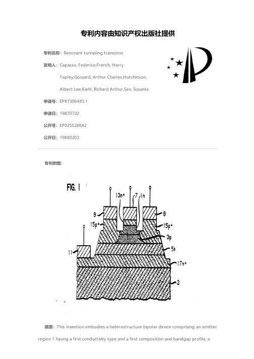
专利名称:Resonant tunneling transistor发明人:Capasso, Federico,French, HarryTapley,Gossard, Arthur Charles,Hutchinson,Albert Lee,Kiehl, Richard Arthur,Sen, Susanta申请号:EP87306485.1申请日:19870722公开号:EP0255288A2公开日:19880203专利内容由知识产权出版社提供专利附图:摘要:This invention embodies a heterostructure bipolar device comprising: an emitter region 1 having a first conductivity type and a first composition and bandgap profile, abase region 3 having a second conductivity type and a second composition and bandgap profile, a collector region 5 having said first conductivity type and having a third composition and bandgap profile, electrical contacts, e.g. 7 and 11, at least to said emitter and collector regions, respectively, and a quantum well between said collector region and said electrical contact to said emitter region, said device being capable of operating such that there are first and third base-emitter voltages and a second base-‐emitter voltage intermediary to said first and third base emitter voltages such that, at said first, second, and third base-emitter voltages, the bottom of the conduction band in at least a portion of said emitter region is below, at, and above, respectively, a quantum resonance of said quantum well, said portion being between said first electrical contact and said quantum well. In one embodiment, a compositionally graded portion of the emitter region is adjacent to the base region, and there is a double barrier in the base region. In another embodiment the quantum well is defined by the emitter and a potential barrier in the base region. Further embodiments have a quantum well between emitter and collector regions or else within the emitter region.申请人:AT&T Corp.地址:32 Avenue of the Americas New York, NY 10013-2412 US国籍:US代理机构:Watts, Christopher Malcolm Kelway, Dr.更多信息请下载全文后查看。
Resonant-tunneling transmission line technology

专利名称:Resonant-tunneling transmission linetechnology发明人:Michael W. Geis,Elliott R. Brown,Stephen J.Eglash,Christopher L. Dennis申请号:US08/916829申请日:19970822公开号:US05825240A公开日:19981020专利内容由知识产权出版社提供摘要:Resonant-tunneling transmission lines in the various architectures rely on discrete or continuous resonant-tunneling heterostructures to actively modify propagating logic signals. One embodiment utilizes amplification of logic signals to counteract ubiquitous losses and distortion associated with any transmission medium. Basically, the logic signal is incrementally reamplified and reshaped as it propagates along the transmission line. Another embodiment is directed to a clocking system that transmits a signal represented by a sinusoid. Then, in proximity to the logic gates or modules, the sinusoid is converted into a square wave that actually clocks the gates and other logic structures. The inventive active transmission line naturally performs this feature, thus enabling clock signal transmission over longer links coupled with sinusoid-to-square wave conversion in a limited area. Still other embodiments implement step or continuous variations in the physical width of the resonant-tunneling transmission line. By manipulating the transmission line width of successive sections of the line, isolation in addition to the logic operation of the input signals is achievable in a simple monolithic circuit design. Further embodiments are directed to oscillator circuits and the control ofthe characteristics of the generated periodic signal.申请人:MASSACHUSETTS INSTITUTE OF TECHNOLOGY 代理机构:Hamilton, Brook, Smith & Reynolds, P更多信息请下载全文后查看。
隧道专业英语词汇

我海瑞克盾构设备-英汉对照英文汉语PROPORTIONAL VALVE BLOCK 流量阀BRAKE VALVE 闸阀DOUBLE PRESTRESS VALVE 流量阀VALVE 闸阀BALL VALVE 球阀BALL VALVE W/LEVER/ 球阀SHUTTLE VALVE 闸阀CHECK VALVE SAE11/2 闸阀NOZZLE 喷嘴PROPORTIONAL VALVE 流量阀PRESSURE REDUCING VALVE 减压阀PLATE 连接块ERECTOR 管片安装机CUTTING WHEEL DRIVE 刀盘主驱动TANK 水箱CYLINDER 液压油缸WAGGON 运输料槽JACK 千斤顶THRUST JACKS UNIT+STROKE MEAS 主推进油缸PLANETARY GEAR 齿轮箱GEAR OIL COOLER 齿轮油冷却器THERMOMETER 0-80 DEGREES C 温度计CONTROL BLOCK 接线板PLATE 连接块MECHANICAL DIRECTIONAL CONTROL 方向控制器PRESSURE CONTROL VALVE 流量阀CONTROL BLOCK 接线板SLIDE BLOCK 滑动轴承阻挡块HYDRAULIK BLOCK 液压阀组PRESSURE REDUCING VALVE 减压阀NON RETURN VALVE 止回阀ONE-WAY RESTRICTOR ZP 闸门DIRECTIONAL CONTROL VALVE 流量阀PRESSURE REDUCING VALVE ZP 流量阀BALL VALVE DN13 球阀BLOCK BALL VALVE 球阀NONRETURN VALVE 止回阀PRESSURE TRANSDUCER 压力传感器HYDRAULIC BLOCK 液压阀组CONTROL BLOCK 接线板CURRENT DIVIDING COIL 线圈PRESSURE FUSE 保险融管PRESSURE SWITCH WITH INDICATIO 压力计SHAFT 连接轴FLOWMETER 流量计INTERLOCK MEANS 管接头COMPRESSED AIR PUMP 压缩空气泵WASHER 垫片CYLINDER HEAD SCREW 螺丝SCREW / M24X360 螺丝NUT M24 螺母 HEXAGON NUT 螺帽FILTER 过滤器ROUND CORD 密封圈SCREW / M16X40 螺丝VENTILATION FILTER 过滤器MEASURING DEVICE 测量装置BINDING 扎带DIVE MOTOR PUMP 排液泵SHEET METAL PACKAGE 盾体连接块ERECTOR PARTS 安装机连接梁RAIL 导轨PRESSURE GAUGE , TYPE 213.53 压力表LAMP 灯泡PUMP 冷却泵THRUST JACKS UNIT+STROKE MEAS 推进油缸COMPENSATOR 补偿器SEAL 密封件PLACA DE GOMA 密封件PLUG 销子LOAD SUPPORT 支架SCREW FITTING 管接头SCREW PUMP 螺旋泵HIGH PRESSURE FILTER 过滤器LEVEL CONTROL 水平控制仪STEEL TANK 水箱SOUND ABSORBER 吸音器PRESSURE GAUGE , TYPE 213.53 压力计REPLENISH-VENTILATION FILTER 通风过滤器GREASE LUBRICATION PUMP UNIT 油脂集中润滑泵GREASE PUMP 200L 油脂泵PRESSURE SWITCH 压力计COUPLING 管接头PIPE 钢管SLEEVE COUPLING 套筒T-PIECE T型块O-RING O型圈REGULATION SYSTEM 气体调节系统FLANGE 法兰WELDING NECK 焊接用连杆LIFTING DEVICE 起吊葫芦PRESSURE TRANSDUCER 压力传感器SHAFT SUPPORT 支架CONTROL 电力控制器GASKET 密封圈SWITCH 压力传感器CRANKING 7,5 KW 压力传感器SPHERICAL PLAIN BEARING 滚珠轴承INSTALLATION 安装PIPE BEND 管接头WELDING NECK 焊接用连杆HOSE 液压管 COVER 盖板 RING 环片 FIXTURE 支座SLIDE BEARING 滑动轴承BEARINGS 滚珠轴承MESH PLATFORM 防滑平台 GASKET 密封圈DISTRIBUTOR 分配器 GATE VALVE 闸阀CLAMP 锁紧接头 THIMBLE 套管LOAD CELL 支座 HOUSING 支座 CHAIN 链条MODULE 支座 AMPLIFIER 沙浆座HIGH PRESSURE CLEANER 高压水喷头BACK FLOW PREVENTION 止回阀CLAMP 锁紧接头PLAIN SLIDE VALVE FLANGE PN16 法兰MOTOR 液压马达HYDRAULIC AGGREGATE 液压阀组HYDRAULIC HAND PUMP 液压手泵DIRECTIONAL CONTROL VALVE 方向阀ONE-WAY RESTRICTOR ZP 闸门RETURN VALVE 回流阀HYDRAULIC FITTING FEMALE 液压接头HYDRAULIC FITTING MALE 液压接头PRESSURE TRANSDUCER 压力传感器BALL VALVE WITH PNEUMATIC DRIV 球阀WIRE BRUSH SEAL 盾尾密封刷 RAIL 支座HEAT EXCHANGER 热交换器BEND 90DEGREE 弯头 ANGLE 角接头SHORT BEND 90 DEGREE 弯头NIPPLE 喷嘴 T-PIECE T型块COUNTER BEARING 沙浆箱轴承DRIVE BEARING 沙浆箱驱动轴承BRACKET 连接件 ELLBOW 90°弯头ANGLE 角接头MAIN DISTRIBUTION 2 电力分配柜EQUIPMENT 电力分配柜 DRUM 电缆卷筒 HOSE 软管THRUST JACKS UNIT+STROKE MEAS 液压阀组SCREW COMPRESSOR 螺杆式空气压缩机WATER UNIT 水冷却单元LEVEL CONTROL WITH WATER FLUSH 水平控制仪BACK FLOW PREVENTION 止回阀PRESSURE GAUGE 压力计CAPASITIVE ROPEPROBE 14 M 连接软管SENSOR 感应器 FIXTURE 支座 GRATING 隔栅PLANETARY GEAR 推进齿轮PRESSURE TRANSDUCER 压力传感器REDUCING FITTING 管接头CLAMPING JAW 锁紧接头CONDUCT 导管 ELECTRIC CABLE 电缆CABLE 电缆 CONDUCT 套管PLANETARY GEAR 推进齿轮LEVEL CONTROL 水平控制仪 SOUND ABSORBER 吸音器SAFESET 安全套件 BRAKE 闸门BOLT DYNAMOMETER 螺旋测力计THREADED ROD 螺纹连杆 SAFETY-BUMPER 缓冲器INCADESCENT LAMP 白炽灯 CABLE CHANNEL 电缆槽CLAMPING JAW 锁紧接头 STEEL TUBE 圆钢EQUIPMENT 电力分配柜 WASHER HV 垫片WELDING NECK 焊接用连杆 CAMERA 摄像头MESH PLATFORM 防滑平台TEMPLATE 模板 PLUG 销子COVER 盖板CRANKING 7,5 KW 发动机 SWITCH 开关CHAIN 链条 THIMBLE 套管CLAMP 锁紧接头 GASKET 密封圈SCREW FITTING 管接头 PRESS FITTINGS 管接头PLACA DE GOMA 连接片SOUND ABSORBER 吸音器THERMOMETER 温度计CLOCK 钟 LOCK 锁NON RETURN VALVE 止回阀AXIAL FULL BEVEL NOZZLE 喷嘴HEATING INSTALLATION 加热器 BAND RECORDER DUAL 计录器AGITATOR 鼓风机/搅拌机FEED PUMP 泵 PUMP 泵DIRECTIONAL SOLENOID VALVE DN5 方向阀PRESSURE REDUCER 减压器 FLOWMETER 流量计AGGREGATE 液体泵站FIXING DEVICE 固定件ERECTOR HEAD 管片安装机机头ATTACHMENT 连接器TRANSFORMER 压力传感器WIRE BRUSH SEAL 盾尾密封刷VENTILATOR 通风机ROPE MEASURING PROBE HOUSING 支座SPRING 弹簧SPHERICAL DISK 连接球CAP 螺帽COMPOUND SLIDE 连接滑块SCREW FITTING 管接头CONNECTOR 继电器HYDRAULIC FEEDER 进料器GATE VALVE 门阀TERMINAL BLOCK 终端阀组SHACKLE 挂钩CLAMP 锁紧接头HIGH PRESSURE CLEANER 高压水枪头BOLT DYNAMOMETER 螺旋测力计BELT 输送带WIRE BRUSH SEAL 盾尾密封刷REVOLVING JOINT 主旋转接头CONSOLE 控制台FREQUENCY CONVERTER 变频器MAIN DISTRIBUTION 1 电力分配柜HIGH CONSISTENCY PUMP 排液泵CONTROL BLOCK 液压阀组HIGH CONSISTENCY PUMP 排液泵HYDRAULIC FEEDER 喂料器T-BLOCK T型块VENTILATOR 通风机CURRENT DIVIDING COIL 线圈MEASURING DEVICE 测量仪BUFFER 垫片GREASE CARTON - SLURRY PUMP 泥浆泵WAGGON 输送料槽JACK 千斤顶CHANGING MAGAZINE 储管器CONTROL CABIN 电力控制柜SUCTION FILTER 过滤器STOP GATE DN80 闸门LEVEL CHECK 水平测量仪CONSOLE 控制台REDUCTION 减压器DIFFUSER 扩散器ROPE CLAMP SYSTEM 缆绳锁紧单元DIFFUSER 蓄能器CHANGING MAGAZINE 储管器ELECTRIC MOTOR 电动马达DAMPING RAIL 缓冲槽VARIABLE DISPLACEMENT PUMP 排液泵O-RING O型圈PROXIMITY SWITCH 接近开关LUBRICATING NIPPLE 喷嘴ROLLER 滚筒FREQUENCY CONVERTER 变频器CONNECTOR 继电器TERMINAL BLOCK 终端阀组BULKHAED GATE 盾体闸门FLUORESCENT LAMP 荧光灯SLIDE BEARING 滑动轴承BAND 带子HEMP 带子FERMIT CAN 油漆PAINT BRUSH 油刷FORK-SHAPED PIECE 连接块BELT 输送带TELEPHONE 紧急电话WELDING NECK 焊接用连杆BUSH 衬套STICKER 标签HOUSING 刀箱T-PIECE T型块CABLE SOCKET 电缆插座SLIDE BEARING 滑动轴承SCREW TENSION CYLINDER M64 M64螺栓拉伸油缸HIGH PRESSURE POWER PACK 高压动力包HIGH PRESSURE HOSE 1600BAR高压油缸HIGH POWER AGGREGATE G20 G20高压泵站INSERT FOR SCREW DRIVER SW 65 SW65套筒INSERT FOR SCREW DRIVER SW 55 SW55套筒POWER SCREW DRIVER HYDRAULIC 液压动力扳手HIGH PRESSURE HOSE 高压油管DISPLACEMENT CYLINDER 移位液压油缸AGGREGAT 液压泵站CONTAINER 20" 20"集装箱SHIELD 盾体INSTALLATION THRUST JACKS 推进千斤顶THRUST JACKS UNIT+STROKE MEAS 推进系统+THRUST CYLINDER 推进油缸CUTTINGWHEEL DRIVE 刀盘驱动SEAL 密封PLANETGEAR 行星齿轮箱MOTOR WATER COOLED 马达水冷却PINION 小齿轮ERECTOR 拼装机PLANETARYGEAR 行星齿轮箱DISPLACEMENT MOTOR 变速马达HUDRAULIC SCHEME/GROUT INJECTION 液压回路/注浆回路HIGH CONSISTENCY PUMP 高压泵WATER CIRCUITS S-317 水循环S-317SLURRY CIRCUIT 泥浆回路BALL VALVE+HYDRAULIC DRIVE 球阀+液压驱动ELECTRIC MOTOR 电动马达PARTICULATE PUMP 小型泵FLANGE BALL VALVE 法兰球阀VACUUM SCHEME 真空装置VACUUMPUMP 真空泵CUTTERHEADMOTOR 刀盘马达HYDR.AGITATOR 液压搅拌机HYDR.THRUST RAM 液压推力缸HYDR.ERECTOR 液压拼装机CIRCULATION PUMP P-0.1 循环泵HYDR.GROUTING 液压注浆PUMP PIPE PIG 清洗泵HYDR.AUXILIARY 1 液压辅助设备1PUMP INTERNAL COOLINGCIRCUIT 内冷却循环泵PUMP DEWATERING COOLINGWATER 抽水泵PUMP WATER HIGHPRESSURE 高压水泵SEGMENT TRANSPORT CRANE 管片起重机SEGMENT TRANSFER CRANE 管片搬运机ROAD-ELEMENT CRANE 道路机EXIT RESERVE 逃出储备 SOCKETS 插座HYDR.OVERCUTTER 液压超挖刀PUMP INDUSTRIALWATER 工业用水泵PUMP GEAROIL 1 齿轮油泵1HYDR.AUXILIARY 2 液压辅助设备2HYDR.FILTERCIRCUIT 液压滤波电路LUBRICATION PUMP 润滑油泵GROUT TANK 1 AGITATOR 浆桶1 搅拌机MOBILE GROUT TANK 1 AGITATOR 移动浆桶1 搅拌机COOLINGSYSTEM HV 2 冷却系统HV 2AUXILIARY RAIL CRANE RIGHT 辅助起重机右DUCT CASSETTE CRANE 管盒起重机PIPE EXTENSION CRANE 管子延伸起重机HEATING MANLOCK 供热人行闸HYDR.ERECTOR EMERGENCY 液压拼装机应急事故DRIVE CABLE REEL 驱动电缆盘PUMP VACUUM ERECTOR 拼装真空泵DRIVE HOSE REEL 驱动软管卷OFFICECONTAINER 办公集装箱CREWCONTAINER 员工集装箱MANLOCK/WORKING CHAMBER 人行闸/工作室EMERGENCY-DEWATERING 应急抽水EFFICIENCY 效率, 功效POWERFACTOR 功率因数SIMULTANEITY 同时发生, 同时SLURRY CIRCUITS AND TUNNEL BELT CONVEYOR 泥水管路及隧道皮带输送机SEGMENT MOULDS 管片模具 GANTRY CRANE 门吊ROLLING STOCK INCL. LOCOMOTIVES 运输车包括牵引机车VENTILATION EQUIPMENT 通风系统TRANSFORMER STATION 变压器SEPARATION PLANT 泥水分离设备GROUT MIXING EQUIPMENT 砂浆搅拌设备COOLING SYSTEMS 冷却系统COMPRESSED AIR PLANTS 压缩空气设备SEGMENT DESIGN 管片设计OD 外径 ID 内径 LENGTH 宽度DISTRIBUTION 布置方式TUNNEL GRADIENT 隧道坡度TUNNEL LENGTH 隧道长度 SHIELD 盾体FRONT SHIELD DIAMETER 盾体前部直径REAR SHIELD DIAMETER 盾体后部直径TBM STEERING MINIMAL HORIZONTAL RADIUS 最小转弯半径CONSTRUCTION OF THE FRONT & REAR SHIELDS 盾体前部、后部结构PRESSURE WALL 压力舱板 SUBMERGED WALL 隔板AIR REGULATION DEVICE 气压调节装置FRONT GATE 前闸门 AGITATOR 搅拌器TAILSKIN 盾尾 DIAMETER 直径TAILSKIN TYPE 盾尾类型TAILSKIN SEAL SYSTEM 盾尾密封系统EMERGENCY TAILSKIN SEAL SYSTEM 紧急盾尾密封系统GREASE LINES 油脂管GROUTING LINES 注浆管GROUTING LINE CLEANING SYSTEM 注浆管清洗系统AIR LOCK 空气闸MAN LOCK 人行闸 NUMBER 数量NUMBER PERSONS 容纳人数 NORM 标准OPERATING PRESSURE 工作压力TEMPORARY MAN LOCK 临时人行闸LENGTH 长度 TYPE 类型 NORM 标准NUMBER PERSONS 容纳人员数OPERATING PRESSURE 操作压力MATERIAL LOCK 材料闸OPERATING PRESSURE 工作压力CUTTING WHEEL (CW) 刀盘 DIAMETER 直径CONSTRUCTION 结构CUTTING WHEEL WITH EXCHANGEABLE TOOLS FROM WITHIN THE ARMS 刀盘带有可从刀盘臂进行更换的刀具SOFT GROUND TOOLS 软土刀具WEAR DETECTION EQUIPMENT 磨损监测系统ROTARY UNIT 旋转中心接头DIRECTION OF ROTATION 旋转方向CENTRE CONIC AREA FLUSHING 中心锥形体部位冲刷CUTTING WHEEL DRIVE 刀盘驱动TYPE OF MAIN DRIVE 主驱动类型MAIN BEARING TYPE 主轴承类型MAX PRESSURE FOR SEAL SYSTEM 密封最高工作压力ELECTRIC MOTOR 电机驱动TOTAL ELECTRICAL POWER 总功率NOMINAL TORQUE 额定扭矩EXCEPTIONAL TORQUE 最大扭矩BREAKOUT TORQUE 脱困扭矩ROTATION SPEED 最大转速OUTSIDE DIAMETER OF MAIN BEARING 柱轴承外径ROTATION DIRECTION 旋转方向LIFE TIME DURATION MAIN BEARING 设计寿命THRUST CYLINDERS 推进油缸QUANTITY 数量DIMENSIONS OF THE THRUST CYLINDERS 油缸尺寸QUANTITY OF THRUST CYLINDER GROUPS 油缸分区数量CYLINDERS WITH STROKE MEASUREMENT SYSTEM 油缸,带有行程及速度量装置SUPPORT 支撑 WORKING PRESSURE 工作压力NOMINAL THRUST FORCE 额定推力MAX. THRUST FORCE 最大推力MAX. EXTENSION SPEED 最大伸出速度RETRACTION SPEED 收回速度ERECTOR CEN STANDARD 管片拼装机CEN 标准GRIPPING SYSTEM 抓取系统DEGREES OF FREEDOM 自由度ROTATION SPEED 回转速度 ROTATION 回转角度MAX SEGMENT WEIGHT 最大提升管片重量RADIO REMOTE CONTROL 无线遥控SPECIFIC LIFT FOR RING BUILDING 管片安装专用提升装置AIR LOCK SHUTTLE TRANSPORTATION SYSTEM IN THE SHIELD 盾机内的穿梭气闸运输系统LIFTING DEVICE 起吊装置TRANSFER CRANE 运输吊机ELECTRIC INSTALLATION CEN STANDARD 电气设备CEN 标准INSTALLED ELECTRIC POWER 功率IP RATING ELECTRIC MOTOR 电机保护等级BACK-UP EQUIPMENT 后配套设备TUNNEL LINES 隧道内管线SLURRY DISCHARGE LINE 泥浆排出管SLURRY FEED LINE 泥浆供应管INDUSTRIAL WATER LINE 工业用水管COMPRESSED AIR LINE 压缩空气管HV CABLE 高压电缆TRAILER STRUCTURE 拖车结构STEEL STRUCTURE TRAILER 拖车钢结构SEGMENT HANDLING SYSTEM 管片吊运系统SEGMENT FEEDER 喂片机SEGMENT CRANE 管片吊机GROUT INJECTION SYSTEM 注浆系统 GROUT TYPE 浆液类型GROUT INJECTION CAPACITY 注浆泵容量 GROUT PUMPS 注浆泵FIXED GROUT TANK 固定砂浆罐STAND BY POSITIONS 备用活塞MOVABLE TANKS 可移动砂浆罐HYDRAULIC INSTALLATION 液压设施WORKING PRESSURE 工作压力AIR LOCK TRANSPORTATION SYSTEM IN THE BACK-UP SYSTEM 后配套系统上的气闸运输系统PLACE RESERVATION 保留空间GREASE STATION 油脂站PNEUMATIC GREASE PUMP 气动油脂泵PNEUMATIC GREASE PUMP 气动油脂泵PNEUMATIC GREASE PUMP 气动油脂泵COMPRESSED AIR UNIT 压缩空气单元ON THE TBM 在盾构机上AIR COMPRESSOR FOR COMPRESSED AIR REGULATION (AIR CUSHI ON) 用于调节压力的压缩空气机(气垫)AIR TANK 储气罐BREATHABLE AIR FILTER DEVICES 呼吸空气过滤设备INDUSTRIAL WATER CIRCUIT 工业用水系统COOLING CIRCUIT 冷却循环系统COOLER TYPE 热交换器类型INTERNAL BOOSTER PUMP 升压泵DISCHARGE BOOSTER PUMP 排出泵INTERMEDIATE TANK 水箱DEWATERING CIRCUIT 排水系统PNEUMATIC PUMP 气动泵PNEUMATIC PUMP FOR INVERT CLEANING 反向清洗的气动泵DIRTY WATER TANK 5M3 污水箱5M3ELECTRIC INSTALLATION 电气设施PRIMARY VOLTAGE 输入电压INSTALLED ELECTRIC POWER 安装的电器系统电源PLC UNIT PLC 单元INDEX OF PROTECTION 保护等级CONTROL CABIN 控制室SUB. DISTRIBUTION PANELS 次级配电柜MAIN DISTRIBUTION PANELS 主配电柜TRANSFORMER MAIN DRIVE MOTOR 主驱动电机变压器TRANSFORMER BACK UP SYSTEM 后配套系统变压器TRANSFORMER SLURRY PUMP P2.1 泥浆泵P2.1变压器MEDIUM VOLTAGE SWITCH 中级开关POWER FACTOR CORRECTION 功率因数补偿EARTH LEAKAGE RELAY 接地泄漏继电器EMERGENCY LIGHTING 应急照明DIESEL GENERATOR 160KVA 柴油发电机160KVAVENTILATION SYSTEM 通风系统SECONDARY VENTILATION 次级通风系统- SILENCER - 消声器- BOOSTER FAN - 鼓风机AIR DUCT CASSETTE DN2,800MM 气管存储筒DN2,800MM EXTENSION SERVICES 延伸作业HV CABLE 10KV 高压电缆10KVEARTHING CABLE 接地电缆SIGNAL CABLE FOR SLURRY PUMPS CONTROL, DATA ACQUISITION CABLE (INCLUDING VMT) 用于泥水泵控制的信号电缆(包括井上井下数据采集、VMT)CCTV OPTICAL FIBRE 用于CCTV信号传输的光缆COOLING WATER 冷却水DEWATERING WATER 排水管EMERGENCY COMPRESSED AIR 紧急压缩空气AIR DUCT 通风管PERSONNEL FACILITIES 员工设施STORAGE AREA 存储区WORKSHOP AREA 工作区RECREATION ROOM 休息室ENGINEER ROOM 工程师室INFIRMARY & TOILET WITH WASHING FACILITIES 医疗设施、洗手间带盥洗装置SLURRY CIRCUIT INSTALLATION 泥浆循环设施SLURRY FLOW RATE 泥浆流量MAIN CIRCUIT ON TBM 在盾构机上的主循环DIAMETER OF SLURRY PIPE ON TBM 盾构机上的泥浆管直径EXCAVATION CHAMBER FLUSHING 开挖舱冲刷BENTONITE NOZZLES LINES 膨润土喷注管BENTONITE NOZZLES LINES 膨润土喷注管CENTRE CONIC AREA FLUSHING 中心锥形体部位冲刷FLUSHING NOZZLES 膨润土冲刷喷嘴FLUSHING PUMP 冲刷泵SUCTION GRID 入口隔栅BY PASS IN SHIELD 在盾体内的旁通VALVES TYPE 阀门类型FLOW METER MEASUREMENT DEVICES 流量测量装置SLURRY LINE PRESSURE SENSORS 泥水管路压力传感器DENSITY MEASUREMENT ON TBM TBM上的密度测量装置DENSITY MEASUREMENT IN THE TUNNEL 隧道内的密度测量装置SLURRY PUMP ON BACK-UP 后配套上的泥浆泵SLURRY PIPES EXTENSION SYSTEM 泥浆管延伸系统SLURRY PIPES STORAGE AREA 泥浆管存储区MAIN CIRCUIT IN TUNNEL 隧道内主循环DIAMETER OF SLURRY PIPELINE IN TUNNEL 隧道内泥浆管直径SLURRY PUMP 排渣泵DIAMETER OF FEED PIPELINE 供应管路直径FEED BOOSTER PUMP 供应泵AUXILIARY EQUIPMENT 辅助设备CCTV SYSTEM CCTV-系统COMMUNICATION SYSTEM 通讯系统GUIDANCE SYSTEM 导向系统TAILSKIN CLEARANCE MEASURING 盾尾间隙测量系统DATA LOGGING SYSTEM 数据采集系统FIRE SUPPRESSION SYSTEM 灭火系统GAS MONITORING SYSTEM 毒气探测系统THRUST CYLINDER 推进油缸ROTARY TRANSMISSION LEADTHROUGH 回转接头EMERGANCY SEAL 紧急密封ELECTROMOTOR 电马达 GEARBOX 齿轮箱PINION 小齿轮 SEAL 密封 PLANETGEAR 行星齿轮箱RACERING 座圈MAIN BEARING 主轴承INSTALLATION THRUST JACKS 推进油缸回路DISPLACEMENT PUMP 变量泵 VACUUMPUMP 真空泵HYDRAULIC SCHEME/ERECTOR 液压图/拼装机DISPLACEMENT PUMP 变量泵FILTER-/COOLING CIRCUIT 滤清器/冷却回路HEAT EXCHAGER 热交换器 SCREWPUMP 螺旋泵HYDRAULIC SCHEME/GROUT INJECTION 液压图/注浆回路GROUTPUMP 注浆泵 SLURRY PUMP 泥浆泵WATER CIRCUIT 水回路 WATER PUMP 水泵SLURRY CIRCUIT 泥浆回路 SLURRY PUMP 泥浆泵HOUSING 壳子 WEEHL 轮子GREASE LUBRICATION 油脂润滑AIRPUMP 空气泵CONTAINER 20" 20"集装箱BRUSH SEAL 盾尾密封刷SEAL SET 密封组DIV.SPARE PARTS SHILD 待定盾体备件BENTONIT NOZZEL 膨润土喷嘴CYLINDER 液压油缸COMPENSATOR 补偿器 BUCKET 铲刀CUTTING KNIFE 齿刀 CUTTINGWHEEL 刀盘FIXING ELEMENTS 固定用元件ERECTOR 拼装机VACCUM PUMP 真空泵 SEAL 密封SUPPORT 支撑 HUSK 支架CYLINDER 油缸 LASER 激光工具ENERGY CHAIN 能量链条FILTERELEMENT 滤芯 CIRCUITS/NETS 回路INSTALLATION THRUST JACKS 推进千斤顶TRANSFORMER 传感器FILTERELEMENT 滤芯 PROP.VALVE 比例阀HYDRAULIC SCHEME/CUTTING WHEEL DRIVE 液压图/刀盘驱动PROP.VALVE 比例阀PRESSUERE SWITCH 压力开关HYDRAULIC SCHEME/ERECTOR 液压图/拼装机REP. KIT VACUUMPUMP 真空泵修理包FILTERELEMENT VAKUUMPUMPE 真空泵滤芯FILTERELEMENT 滤芯PRESSURESWITCH 压力开关PRESSURE GEAUGE 压力表PROP.VALVE 比例阀HYDRAULIC SCHEME/AUXILARY SYSTEMS 液压图/辅助系统DISPLACEMENT PUMP 变量泵NON RETURN VALVE 止回阀PRESSUERE SWITCH 压力开关FILTER-/COOLING CIRCUIT 滤清器/冷却回路DISPLAY 指示器HYDRAULIC SCHEME/GROUT INJECTION 液压图/注浆系统DISPLACEMENT PUMP 变量泵CYLINDER 液压油缸PISTON 活塞泵WATER HIGH PRESSURE UNIT 高压水系统HIGHPRESSUREAGGREGAT 高压站REP. KIT PUMP 泵修理包REP. KIT AGGREGAT 高压站修理包WEAR KIT PUMP 泵易损件修理包WEAR KIT AGGREGAT 高压站易损件修理包TEMP.SWITCH 温度开关 PRESSURE SWITCH 压力开关WATER CIRCUIT 水回路HOSE DN150 DN150的管子FLOWMETER 流量计SLURRY CIRCUIT 泥浆回路FLOWMETER 流量计BALL VALVE DRIVE 球阀驱动COMPENSATOR 补偿器 PACKING 密封 O-RING 密封 SEAL 密封HOUSING 壳子 HUSK 架子 RING 环 O-RING 密封环SLURRY PUMP 泥浆泵REP.KIT 修理包SEAL SET 密封组件SEALING PLATE 密封盘HYDRAULIC SCHEME/GROUT INJECTION 液压图/注浆系统COMPRESSED AIR SCHEME 压缩空气系统REGULATOR 调节器PRESSURE TRANSDUCER MIX 压力传感器PRESSURE RED: VAVE 红色压力阀CONTROL LEVER 控制杆 JOYSTICK 控制器POWER SUPPLY 电力供应POWER SUPPLY UNIT 电力供应单元FREQUENCY CONVERTER - INTERFAC 变频器- 界面FREQUENCY CONVERTER 变频器DIGITAL MEASURING DEVICE 数字测量装置ABSOLUT VALUE INDICATOR 绝缘值指示器CARBON MONOXIDE SENSOR 一氧化碳感应塞METHANE SENSOR 甲烷感应塞OXYGEN SENSOR 氧气感应塞COMMUNICATION SYSTEM 通讯系统INTERFACE MODULES 模块PROCESSOR 处理器PERIPHERAL SYSTEM S7-300 外围系统S7-300DIGITAL INPUT SM321 数字输入SM321FRONT PLUG 392 40-POLIG 前塞392 40-POLIGPLUG-PROFIBUS 塞子-PROFIBUSSOFTWARE 软件ANALOG INPUT 模拟输入ANALOG OUTPUT SM332 模拟输出SM332PLUG 塞子COLOUR CAMERA WITH INFRA-RED 红外线彩色像头LEVEL CARD 液位卡ELECTRIC LIGHT BULB 28V/40MA 灯泡28V/40MABUSH BUTTOM 按钮PRESSURE SWITCH WITH ML24V 22, ML24V 22压力开关SPHERICAL CAP RED 红色球形盖SPHERICAL CAP GREEN 绿色球形盖SPHERICAL CAP YELLOW 黄色球形盖CONTROL CARD 控制卡DIGITAL CARD 数字卡AMPLYFYING CARD 信号放大卡CONTROL CARD 控制卡SEGMENTFEEDER 管片喂送器CYLINDER 油缸DIV.SPARE PARTS SEGMENTFEEDER 待定管片喂送器备件SEGMENTCRANE 管片吊机GEAR MOTOR 齿轮马达DRIVE MOTOR 驱动马达SPARE PART PACK SEGMENT CRANE 管片吊机备件包DIV.SPARE PARTS 待定备件DIV.SPARE PARTS ERECTORPULT 待定拼装机备件拼装机控制面板SCREW TENSION CYLINDER M42 M42螺栓拉伸油缸SCREW TIGHTENING DEVICE M60 M60螺栓上进装置HIGH PRESSURE POWER PACK 高压动力包HIGH-PRESSURE HOSE 高压油管HIGH PRESSURE HOSE 1600BAR高压油缸HIGH POWER AGGREGATE G20 G20高压泵站HIGH PRESSURE HOSE 高压油管INSERT FOR SCREW DRIVER SW 65 SW65套筒INSERT FOR SCREW DRIVER SW 55 SW55套筒POWER SCREW DRIVER HYDRAULIC 液压动力扳手DISPLACEMENT CYLINDER + AGGREGAT 移位油缸+液压泵站TOOL BOX 工具箱CABLE SHEARS 电缆剪SCREW DRIVER 螺丝刀SOCKET WRENCH SET 12K 12K套筒扳手装置DRILLING MACHINE 钻机GAS SOLDERING IRON SET气体烙铁 TIN 锡罐MULTIMETER 万用表 PLIERS 钳子 KALIBRATION DEVIC 校准装置TORCH 手电筒 TWIST DRILL 螺旋钻INDICATION 指示器 FAN 风扇 TORQUE WRENCH 扭矩扳手GRINDER 电砂轮 COAL DRILL 煤钻SEGMENT DATA: 管片参数:OUTSIDE DIAMETER: 15,000MM 外径: 15,000MMINSIDE DIAMETER 13,700MM 内径: 13,700MMLENGTH 2,000MM 宽度: 2,000MMRING DISTRIBUTION: 9+1 管片分布: 9+1MIX SHIELD WITH BACK-UP SYSTEM 混合式盾构机及后配套系统SHIELD BODY 盾体SEGMENTAL STEEL STRUCTURE (FRONT AND REAR SHIELDS) 钢结构块(前盾和后盾)PRESSURE WALL 压力壁SUBMERGED WALL (AIR BUBBLE CHAMBER) 分隔板(气泡调压舱) PRESSURE SENSORS 土压传感器ACCESS DOOR IN THE PRESSURE WALL 压力舱壁中的进入门ACCESS DOOR IN THE SUBMERGED WALL 分隔板中的进入门FLANGE MANLOCK 人闸法兰LANGE FOR MATERIAL LOCK 材料闸法兰MAIN DRIVE SUPPORT 主驱动支架AGITATORS Æ1,900MM 搅拌器Æ1,900MMFRONT GATE 前闸门PROTECTION GRID 保护隔条FLUSHING CIRCUIT IN THE EXCAVATION CHAMBER 开挖舱内的冲洗回路19 X TRIPLE THRUST CYLINDERS 19 X 3个推进油缸INJECTION POINTS 2” FOR SHIELD LUBRICATION 2”盾体润滑注入点TAILSKIN 盾尾SANDWICH TYPE STEEL STRUCTURE 夹层“三明治”式钢结构ROWS OF WIRE BRUSH SEAL 排密封钢丝刷EMERGENCY SEAL SYSTEM 紧急密封系统INJECTION PIPES FOR TAILSKIN GREASE PER GREASE CHAMBER 每个油脂舱盾尾注脂管SINGLE GROUT INJECTION CHANNELS FOR MORTAR 单液砂浆注入管道GROUT AND GREASE PIPES ARE INTEGRATED IN THE TAILSKIN STEEL STRUCTURE 注浆管和注脂管集成在盾尾钢结构里CUTTING WHEEL 刀盘SPOKES STAR DESIGN 星形轮辐设计CENTRE CONE TO CONNECT THE CUTTING WHEEL THE MAIN DRIVE UNIT 中心锥用于连接刀盘和主驱动单元WITH MAN ACCESS TO CHANGE THE TOOLS FROM WITHIN THE ARMS有人员通道,可以从刀盘臂内进入进行换刀FIRST DRESS OF CUTTING TOOLS INCLUDING EXCHANGEABLE CUTTING TO OLS, STANDARD CUTTING TOOLS AND STANDARD BUCKET LIPS, 初装刀,包括可更换刀具、标准切刀和标准铲刀COPY CUTTER, 仿型刀CENTER FLUSHING CIRCUIT EQUIPMENT 中心冲刷设备ROTARY UNIT DN150MM FOR BENTONITE 膨润土旋转单元DN150MM STANDARD SCRAPERS EQUIPPED WITH WEAR DETECTION EQUIPMENT 标准刮刀,带磨损监测装置BUCKET LIPS EQUIPPED WITH WEAR DETECTION EQUIPMENT 铲刀,带磨损监测装置MAIN DRIVE INCLUDING MAIN BEARING Ø 8M AND LUBRICATION SYSTEM主驱动,包括主轴承Ø 8M 和润滑系统INNER AND OUTER SEALING SYSTEM 内外密封系统MAIN BEARING Æ8,000MM 主轴承Æ8,000MMELECTRIC MOTOR 250KW WITH SAFE SET 电机250KW,带安全单元PLANETARY GEAR BOX 行星齿轮箱FREQUENCY DRIVE UNITS 变频驱动单元INSTALLED POWER 3,500KW 安装功率3,500KWSEGMENT ERECTOR 管片安装机ERECTOR BEAM 安装机梁BASE FRAME 基架ROTATION FRAME WITH TELESCOPE 伸缩旋转架TRAVERSE WITH ERECTOR HEAD 横梁及安装机头LIFT FOR RING BUILDING 管片安装升降系统ERECTOR BEARING 安装机轴承REMOTE CONTROL (RADIO) 遥控设备(无线和线控)AUXILIARY CRANE FOR INSTALLATION OF THE AUXILIARY INVERT SEGMENT 辅助吊机,用于安装辅助仰拱块COUNTER WEIGHT 平衡块VACUUM GRIPPING DEVICE INCL. VACUUM PUMP 真空抓取系统,包括真空泵MAN LOCK INCL. EACH 人闸,每个包括DOUBLE CHAMBER 两个舱体STEELWORK 钢架ACCORDING TO DIN EN 12110 依据DIN EN 12110PIPES AND INSTALLATIONS 管道和安装设施AIR LOCK IS EQUIPPED WITH FLANGE 空气闸,有法兰盘MATERIAL LOCK INCL. EACH 材料闸,每个包括STEELWORK 钢架SINGLE CHAMBER 单舱体ACCORDING TO DIN EN 12110 依据DIN EN 12110PIPES AND INSTALLATIONS 管道和安装设施HYDRAULIC SYSTEM 液压系统THRUST CYLINDER HYDRAULIC 推进油缸液压系统GROUT PUMPS HYDRAULIC 砂浆泵液压系统ERECTOR HYDRAULIC 管片安装机液压系统ERECTOR AUXILIARY HYDRAULIC 管片安装机辅助液压系统COPY CUTTER HYDRAULIC 仿型刀液压系统AUXILIARY HYDRAULIC (FRONT GATE, BENTONI TE NOZZLES, …)辅助液压系统(前闸门、膨润土喷嘴、….)FILTER AND COOLING CIRCUIT 过滤器和冷却回路ELECTRICAL EQUIPMENT 电气设备TRANSFORMERS 变压器MAIN AND SUB DISTRIBUTION 主、副配电柜LIGHTING AND EMERGENCY LIGHTING WITH BATTERY 照明及应急照明系统,备电池CONTROL VOLTAGE SYSTEM 电压控制系统CONTROL CABIN WITH AIR CONDITIONING DEVICE 控制室,带空调设备EARTH LEAKAGE RELAY UNITS 接地泄漏继电器MEDIUM VOLTAGE SWITCH UNITS 中压开关单元COMPENSATION UNITS 补偿单元ELECTRICAL EQUIPMENT (CONTINUE) 电气设备(续)EMERGENCY STOPS 紧急停止开关PLC CONFIGURATION S7 INCL. USV BATTERY PLC系统S7 ,包括USV 电池HV CABLE DRUM INCL. 200M HV CABLE 高压电缆卷筒,包括200M 高压电缆EARTH CABLE BOX 接地电缆盒COMMUNICATION CABLE DRUM INCL. 200M OF COMMUNICATION CABLE 通讯电缆卷筒,包括200M通讯电缆SECONDARY VENTILATION SYSTEM 二次通风系统BOOSTER FAN 鼓风扇SILENCERS 消声器AIR DUCT CASSETTE W/O AIR DUCT 风管盒,不含风管HANDLING DEVICE FOR AIR DUCT CASSETTE 风管盒操作设备BACK-UP GANTRIES AND INSTALLATION: 后配套拖车及装备:GANTRY 1 RUNNING ON AUXILIARY RAILS 1号拖车,行走于辅助轨道BRIDGE SECTION 连接桥部分GANTRY 2 RUNNING ON AUXILIARY RAILS 2号拖车,行走于辅助轨道SEGMENT FEEDER RUNNING ON AUXILIARY INVERT SEGMENT 喂片机,行走于辅助仰拱块上TURNING TABLE 转板SEGMENT CRANE 1 管片吊机1SEGMENT CRANE 2 管片吊机2ROAD ELEMENT CRANE 箱涵吊机SET OF CRANES TO HANDLE THE AUXILIARY RAILS/ CONSOLES 套吊机设备,用于操作辅助轨道/托架PLACE RESERVATION FOR THE AIR LOCK SHUTTLE TRANSPORT 预留空气闸穿梭运输的空间GREASE PUMP STATION 油脂泵站GREASE PUMP FOR MAIN DRIVE 主驱动油脂泵GREASE PUMP FOR LABYRINTH (HBW) 迷宫环油脂泵(HBW)CONTROL CABIN WITH AIR CONDITIONING 控制室,带空调设备COMMUNICATION SYSTEM (10 TELEPHONES) 通讯系统(10 部电话机)CCTV SYSTEM INCL. 4 CAMERAS CCTV 系统,包含4个摄像机DIESEL GENERATOR 柴油发电机FIRE FIGHTING EQUIPMENT 灭火设备GAS DETECTION EQUIPMENT 气体检测设备STORAGE AREA WITH SHELVES 存储区域,含架子STORAGE AREA FOR THE TUNNEL PIPES 隧道内管子存储区域WORKSHOP AREA WITH WORK BENCH (W/O TOOLS) 工作台(不含工具)操作区域RECREATION ROOM WITH AIR CONDITIONING 休息室,带空调ENGINEER ROOM WITH AIR CONDITIONING 工程师办公室,带空调INFIRMARY & TOILET WITH WASHING FACILITIES 医务及盥洗室,有清洗设施AUXILIARY RAILS INCL. CONSOLES AND THE INVERT SEGMENT ARE TO BE PROVIDED BY THE BUYER. 辅助轨道(包括托架,仰拱块)由买方提供DATA ACQUISITION SYSTEM 数据采集系统INDUSTRIAL PC (LOCATED AT THE SURFACE) WITH MODEM 工业计算机(在地面上) ,带调制解调器SCREEN AND MESSAGES IN CHINESE AND ENGLISH LANGUAGES 显示屏及中英文信息SOFTWARE (WINDOWS, EXCEL, PC ANYWHERE, WORD) IN ENGLISH 英文软件(WINDOWS, EXCEL, PC ANYWHERE, WORD)MODEM TO CONNECT TO THE SURFACE (WITHOUT TELEPHONE CABLE)连接到地面的调制解调器(不含电话线)TELEPHONE CABLE DRUM 电话电缆卷鼓GUIDANCE SYSTEM (SLS-T APD) 导向系统(SLS-T APD)LASER STATION 激光站ELS TARGET ELS 电子靶INDUSTRIAL PC (LOCATED ON THE MACHINE) 工业计算机(在机器上) SOFTWARE IN ENGLISH 英文软件DATA ACQUISITION UNIT 数据采集单元PRE-CALCULATION OF THE RING SEQUENCE 管片序列预计算TAILSKIN MEASUREMENT SYSTEM 盾尾测量系统SLURRY CIRCUIT ON THE TBM TBM上的泥水回路OUTPUT 3,000M³/H 输出3,000M³/HSET OF SLURRY PIPES ON THE TBM Æ500MM 套TBM上的泥水管Æ500MM DENSITY MEASUREMENT SYSTEM 密度测量系统1 SET OF VALVES DN 500MM 1 套阀,DN 500MMBY PASS IN SHIELD 旁通站,在盾体上FLOW METER DEVICES 流量表BOOSTER PUMP FOR CENTER FLUSHING 中心冲刷增压泵DISCHARGE PUMP 300 SHG TYPE 排泥泵,型号300 SHGSLURRY PIPES EXTENSION SYSTEM (HOSE LOOP) 泥水管延伸系统(胶管回路) SLURRY CIRCUIT IN THE TUNNEL 隧道内的泥水回路OUTPUT DISCHARGE LINE : 3,000M³/H 排泥管输出: 3,000M³/HOUTPUT FEED LINE : 2,700M³/H 进泥管输出: 2,700M³/H200M OF DISCHARGE AND FEED PIPES Æ600MM 200M 排泥管和进泥管Æ6 00MMDENSITY MEASUREMENT SYSTEM 密度测量装置BY PASS IN SHAFT 竖井内的旁通PRESSURE SENSORS INSTALLED ON THE DISCHARGE LINE INCL. COMMUNI CATION CABLE 压力传感器,安装在排泥管上,包括通讯电缆DISCHARGE PUMP 300 SHG TYPE INCL. TRANSFORMER AND MEDIUM SWITC H UNIT 排泥泵,类型300 SHG,包括变压器和中压开关单元FEED PUMP 14/12 GGG EXCL. TRANSFORMER AND MEDIUM SWITCH UNIT进泥泵,14/12 GGG ,不包含变压器和中压开关单元GROUT INJECTION SYSTEM 砂浆注入系统INJECTION PUMP KSP 20 注浆泵KSP 20FIX TANK WITH AGITATOR 固定砂浆罐,带搅拌器TRANSPORT TANK WITH AGITATOR 运输罐,带搅拌器CONTROL PANEL 控制面板MANUAL SWITCH TO CONNECT THE SPARE LINES 人工开关,用来连接备用管线AUTOMATIC REGULATION SYSTEM 自动调节系统GROUT LINES CLEANING DEVICE 注浆管清洁设备PIPES, MEASUREMENT DEVICES AND INSTALLATION 管子、测量设备及配备INDUSTRIAL WATER CIRCUIT 工业水回路CLOSED TYPE CIRCUIT 关闭回路BOOSTER PUMP 增压泵INDUSTRIAL WATER TANK 工业水箱SINGLE HOSE REEL 单胶管卷轴DEWATERING CIRCUIT 排水回路DEWATERING PUMP IN SHIELD 排水泵,在盾体上DEWATERING PUMP IN THE BACK UP SYSTEM 排水泵,在后配套上WASTE WATER TANK 废水箱。
- 1、下载文档前请自行甄别文档内容的完整性,平台不提供额外的编辑、内容补充、找答案等附加服务。
- 2、"仅部分预览"的文档,不可在线预览部分如存在完整性等问题,可反馈申请退款(可完整预览的文档不适用该条件!)。
- 3、如文档侵犯您的权益,请联系客服反馈,我们会尽快为您处理(人工客服工作时间:9:00-18:30)。
a r X i v :c o n d -m a t /9612146v 1 16 D e c 1996Resonant Tunneling through Multi-Level and Double Quantum Dots T.Pohjola 1,2,J.K¨o nig 2,M.M.Salomaa 1,J.Schmid 3,H.Schoeller 2,and Gerd Sch¨o n 1,21Materials Physics Laboratory,Helsinki University of Technology,02150Espoo,Finland 2Institut f¨u r Theoretische Festk¨o rperphysik,Universit¨a t Karlsruhe,76128Karlsruhe,Germany3Max-Planck-Institut f¨u r Festk¨o rperforschung,70569Stuttgart,Germany(February 1,2008)We study resonant tunneling through quantum-dot systems in the presence of strong Coulomb repulsion and coupling to the metallic leads.Motivated by recent experiments we con-centrate on (i)a single dot with two energy levels and (ii)a double dot with one level in each dot.Each level is twofold spin-degenerate.Depending on the level spacing these sys-tems are physical realizations of different Kondo-type ing a real-time diagrammatic formulation we evaluate the spectral density and the non-linear conductance.The latter shows a novel triple-peak resonant structure.73.40.Gk,72.15.Qm,73.20.Dx,73.50.Fq Quantum transport of electrons through discrete en-ergy levels in quantum dots has been studied both ex-perimentally [1,2]and theoretically [3–8].In small dots the Coulomb repulsion is strong and may yield the dom-inant energy scale,which gives rise to Coulomb block-ade phenomena (see e.g.Refs.[4–8]for single dots and Refs.[9–12]for multiple dots).At high temperatures,or when the coupling between the dots and metallic leads is weak,the electrons tunnel through the system sequen-tially.At low temperatures and for strong coupling to the leads resonant tunneling processes contribute signif-icantly to the current [3,13–17].The purpose of this Letter is to investigate electronic transport phenomena through two ultrasmall quantum-dot systems:(i)a single dot with two energy levels and (ii)a double dot with a single level in each dot (seeFig.1).We will show that the two models can be mappedonto each other.Thus,it is sufficient to concentrate onone,the single-dot model with two levels.In both caseswe assume strong Coulomb repulsion between the elec-trons,such that we have to consider only two chargestates,e.g.the empty or the singly-occupied dot sys-tem.We further allow for strong coupling between thequantum dot(s)and the metallic leads adjacent to them.This gives rise to resonant tunneling and –as has beenshown for a single dot with one energy level [15–17]–nonequilibrium Kondo effects.In the following we con-sider the case with vanishing magnetic field.Accordinglythe single-electron states are spin-degenerate,which is aprerequisite for Kondo effects.We suggest that the mod-els could be realized experimentally in a setup resemblingthose in Refs.[18–21].A systematic description of resonant tunneling phe-nomena has been developed in Refs.[3,15,22]in terms of a real-time diagrammatic technique.It has been applied to the problems of electron transport through a single-level quantum dot as well as through a small metal island,both connected to reservoirs via tunnel junctions.In the quantum dot Kondo-type effects manifest themselves as a zero-bias maximum in the differential conductance.Fur-thermore,a zero-bias minimum has been predicted for the case where the level lies above the electrochemical po-tentials of the reservoirs [15].Generalizing this method we calculate the spectral density of the two-level dot and the differential conductance for the current through the dot.As novel result we find a multiply peaked resonant structure both in the spectral functions and the differen-tial conductance.When the two levels in the dot are po-sitioned below the electrochemical potentials of the leads a triple-peak structure emerges in the nonlinear conduc-tance:a zero-bias maximum with one satellite peak on each side.When the levels lie above the electrochemi-cal potentials the peaks turn into notches.Depending on the level spacing our model interpolates between an S =1/2and an S =3/2Kondo-type model (generalized to include transitions between all ’spin states’).We denote the two energy levels of the dot by ε+and ε−(the choice of +and −arises from the eigenstates of the double dot system).Both levels are spin-degenerate,εi ↑=εi ↓=εi for i ∈{+,−}.The Hamiltonian is a gen-eralization of the Anderson model,H =H 0,D +H 0,res +H T .The term H 0,D = iσεiσc †iσc iσ+U 0n D (n D −1)describes the isolated quantum dot.The interaction of the electrons in the dot is accounted for by U 0,with n D = iσc †iσc iσbeing the electron number.The elec-trons in the reservoirs are taken to be non-interacting,H 0,res = α∈{R ,L } kσεαkσa †αkσa αkσ.The tunneling Hamiltonian H T = αkiσ T αkiσc †iσa αkσ+h .c . describes tunneling between the dot and the reservoirs.The double-dot system coupled in series between two reservoirs as shown in Fig.1with one spin-degenerate level in each dot is described by the Hamiltonian H =H 0,D +H 0,res +H t +H T .The Hamiltonian of the two capacitively coupled dots is H 0,D = dσεdσc †dσc dσ+U 12n l n r +U 0 d n d ↑n d ↓.In addition to the terms re-ferring to both dots it contains an additional interaction term U 12n l n r .The index d ∈{l ,r }denotes the left or right dot,respectively.The term H t = σ t c †l σc r σ+h .c . describes the tunneling between the dots,while the1tunneling Hamiltonian H T is modified such that it only couples each dot to the lead adjacent to it.The double-dot model can be mapped onto the two-level single-dot model in the regime of large charging energy,i.e.,when U0and U12are larger than all other energy scales of the system.Then it is sufficient to consider only two adjacent charge states of the dou-ble dot.For appropriate values of a gate voltage cou-pled to the dots these states are the empty and the singly charged dot system.Then,wefirst solve the ex-act eigenstates of the double dot isolated from the leads, i.e.,the eigenstates of H0,D+H t.They are symmetric and antisymmetric combination of the single-dot states in the left and right-hand dots|+ =α|l +β|r and |− =β|l −α|r ,with energiesε+andε−,respectively. The tunneling H T couples the leads to these new eigen-states.Thus the effective tunneling matrix elements are T L,+=αT,T R,+=βT,T L,−=βT,T R,−=−αT. Except for this modification of the matrix elements the double-dot system coincides with the two-level single dot. The mapping is not possible if we consider doubly-occupied states.The interaction between electrons in the same dot is stronger than between electrons in different dots.Hence two electrons in a double dot prefer to stay in different dots,and the low energy two-electron states are formed from these single-electron states only.In contrast in a single dot the two-electron states are composed of all single-electron states.By symmetry,in the case of three and four electron states the mapping is possible again. Physical quantities of interest can be expressed as quantum statistical averages.In particular,the d.c.cur-rent through the quantum dot takes the formI=I L=−I R=−ie¯h ∞−∞dωΓR iσΓL iσtrochemical potentials we refer to the renormalized mea-surable level positions.Finally,we choose the temper-ature k B T=0.02Γ,whereΓ=ΓL+ΓR provides the energy scale,such that the thermal energies are always lower than the level spacing in the dots and much lower than the charging energy.In the spectral densities A i(ω)there appear a com-plex,energy-dependent self-energy term which yields a broadening as well as renormalization of the dot levels. The energy-dependence of the self-energy term is due to the resonant-tunneling processes,and it results in a non-trivial functional form of the spectral functions.On top of this structure Kondo-type resonances may appear as a sharp peaked structure at the position(s)of the electro-chemical potential(s).These general effects of resonant tunneling have been found already in the investigations of a single one-level quantum dot[15,17].We keep the lower level below the electrochemical po-tentials of the leads such thatε+<∼−Γ.Tuning the upper levelε−=ε++∆εallows a crossover from the one-level limit,ε−→+∞,to a fourfold-degenerate level,ε+=ε−.For the single-dot model the level separation ∆εreflects the actual physical level separation,whereas it is proportional to the coupling strength between the two dots for the double-dot model.In the limit of in-finite level separation the spectral density A+(ω)repro-duces results obtained before for a single level[15,17]. These are the level renormalization and broadening,as well as–forε+<∼−Γ–Kondo-type resonances at the electrochemical potentials of the leads.For a low lying level this corresponds to the S=1/2Kondo problem, however generalized to a nonequilibrium situation if a transport voltage is applied.When the second level is included,the Kondo peak of the single-level model persists.However,the renormal-ization effect is stronger and,as long asε+,ε−<∼−Γ, a further peak in the spectral functions appears(see the dashed curves in Fig.2).This peak is shifted from the electrochemical potentials by∆εbelow(above)the Kondo peak in the spectral function for the lower(up-per)level.In the other extreme of zero level separation we have a fourfold degenerate case,and the model corre-sponds approximately to a spin S=3/2single-channel Kondo model(in the limit of low lying levels,further-more transitions between all’spin states’are allowed in the present case).In this case the resulting spectral func-tions are equal to each other and have a much more pro-nounced Kondo peak(see the solid curve in Fig.2)than in the single level case.The large resonant peak,seen whenε+=ε−,can be viewed as two Kondo peaks being on top of each other. When the degeneracy is lifted the peak splits into two, separated by∆ǫ.One peak remains pinned at zero since the spin-degeneracy of the levels continues to lead to a Kondo peak.This result differs from the situation where the spin degeneracy of a single level is lifted by a magneticfield[15].When the upper level is lifted far above the lower one the properties of the system approach those ofa single-level dot thus exhibiting just one Kondo peak.The spectral functions are normalized.Since we have neglected multiple occupancy,the normalization is∞−∞dωA iσ(ω)=p0+p iσ,(5)where p0and p iσare the probabilities of an empty dot and that with single electron state iσoccupied.This expression allows us to relate differences in the magni-tudes of the spectral functions to differences in occupa-tion probabilities,e.g.when the spectral functions corre-sponding to different levels are compared to each other.The bias voltage has the effect of splitting all the res-onant peaks in the spectral functions by eV,see Fig.3.The peaked structure of the spectral functions is reflected in a novel structure in the nonlinear conductance,see Fig.4.Instead of a single zero-bias peak,known from the single level dot,there appear now three sharp res-onant peaks between the broad peaks corresponding to the renormalized energy levels.The zero-bias anomaly, characteristic for the single level case remains,but two additional satellite peaks appear at eV=±∆ε.When the level separation is increased the new peaks decrease in size while the peak at zero bias remains unchanged.When the levels lie above the electrochemical potentials, the nonlinear conductance exhibits a triplet of minima with one minimum at the electrochemical potentials and two satellites on each side.When the levels are on op-posite sides of the electrochemical potentials the spectral functions as well as the conductance show very varied structures,which are not easily classified.The systems considered here have not yet been inves-tigated experimentally.Ralph and Buhrman[18]have measured tunneling–enhanced by the Kondo effect–through a localized state of an impurity equivalent to a single one-level dot.Some unexplained features in their results may be due to the existence of the other levels above the electrochemical potentials.The model of a single-or two-level dot with only one electron in it could possibly be realized with the setup used by Tarucha et al.[20].They argue that they can resolve situations with one or few one spin-degenerate levels and one or few elec-trons in the dot.In particular,they report that a third electron inserted into the dotfinds two spin-degenerate levels whose separation can be continuously varied by a magneticfield.In this system,if the gate voltage isfixed near thefirst or third conductance peak the single-or double-level dot is realized,respectively.The difference should be observable in the nonlinear conductance pro-vided that the zero-bias anomalies can be resolved.The relevant parameters reported in Ref.[20]–the coupling strength(tunneling rate)Γ,voltage,and temperature–are already close to those used in our calculations.3In conclusion,we have described electronic transport through a two-level quantum dot and a single-level dou-ble dot coupled between reservoirs.A real-time diagram-matic technique provides a very general tool for the de-scription of various systems,both in the perturbative and nonperturbative regime.We have found a novel triple-peak structure in the nonlinear conductance of these sys-tems and suggest experiments where it is observable.ACKNOWLEDGMENTSWe are grateful to L.P.Kouwenhoven,M.Paalanen, and J.Pekola for discussions.This work has been sup-ported by the“Deutsche Forschungsgemeinschaft”as part of“Sonderforschungbereich195.”One of us(GS) also gratefully acknowledges the support through an A.v.Humboldt Research Award of the Academy of Fin-land.−2.0−1.00.0 1.0ω/Γ0.00.20.4Α(ω)Γ−4.0−2.00.0eV 0.00.5g (V )−0.80.00.80.00.5。