01_UM14_Honda_Yasufumi_Engine-Mount-Force-Strength-Design_Rapid-Start
NuMicro N9H30系列开发板用户手册说明书
NuMicro®FamilyArm® ARM926EJ-S BasedNuMaker-HMI-N9H30User ManualEvaluation Board for NuMicro® N9H30 SeriesNUMAKER-HMI-N9H30 USER MANUALThe information described in this document is the exclusive intellectual property ofNuvoton Technology Corporation and shall not be reproduced without permission from Nuvoton.Nuvoton is providing this document only for reference purposes of NuMicro microcontroller andmicroprocessor based system design. Nuvoton assumes no responsibility for errors or omissions.All data and specifications are subject to change without notice.For additional information or questions, please contact: Nuvoton Technology Corporation.Table of Contents1OVERVIEW (5)1.1Features (7)1.1.1NuMaker-N9H30 Main Board Features (7)1.1.2NuDesign-TFT-LCD7 Extension Board Features (7)1.2Supporting Resources (8)2NUMAKER-HMI-N9H30 HARDWARE CONFIGURATION (9)2.1NuMaker-N9H30 Board - Front View (9)2.2NuMaker-N9H30 Board - Rear View (14)2.3NuDesign-TFT-LCD7 - Front View (20)2.4NuDesign-TFT-LCD7 - Rear View (21)2.5NuMaker-N9H30 and NuDesign-TFT-LCD7 PCB Placement (22)3NUMAKER-N9H30 AND NUDESIGN-TFT-LCD7 SCHEMATICS (24)3.1NuMaker-N9H30 - GPIO List Circuit (24)3.2NuMaker-N9H30 - System Block Circuit (25)3.3NuMaker-N9H30 - Power Circuit (26)3.4NuMaker-N9H30 - N9H30F61IEC Circuit (27)3.5NuMaker-N9H30 - Setting, ICE, RS-232_0, Key Circuit (28)NUMAKER-HMI-N9H30 USER MANUAL3.6NuMaker-N9H30 - Memory Circuit (29)3.7NuMaker-N9H30 - I2S, I2C_0, RS-485_6 Circuit (30)3.8NuMaker-N9H30 - RS-232_2 Circuit (31)3.9NuMaker-N9H30 - LCD Circuit (32)3.10NuMaker-N9H30 - CMOS Sensor, I2C_1, CAN_0 Circuit (33)3.11NuMaker-N9H30 - RMII_0_PF Circuit (34)3.12NuMaker-N9H30 - RMII_1_PE Circuit (35)3.13NuMaker-N9H30 - USB Circuit (36)3.14NuDesign-TFT-LCD7 - TFT-LCD7 Circuit (37)4REVISION HISTORY (38)List of FiguresFigure 1-1 Front View of NuMaker-HMI-N9H30 Evaluation Board (5)Figure 1-2 Rear View of NuMaker-HMI-N9H30 Evaluation Board (6)Figure 2-1 Front View of NuMaker-N9H30 Board (9)Figure 2-2 Rear View of NuMaker-N9H30 Board (14)Figure 2-3 Front View of NuDesign-TFT-LCD7 Board (20)Figure 2-4 Rear View of NuDesign-TFT-LCD7 Board (21)Figure 2-5 Front View of NuMaker-N9H30 PCB Placement (22)Figure 2-6 Rear View of NuMaker-N9H30 PCB Placement (22)Figure 2-7 Front View of NuDesign-TFT-LCD7 PCB Placement (23)Figure 2-8 Rear View of NuDesign-TFT-LCD7 PCB Placement (23)Figure 3-1 GPIO List Circuit (24)Figure 3-2 System Block Circuit (25)Figure 3-3 Power Circuit (26)Figure 3-4 N9H30F61IEC Circuit (27)Figure 3-5 Setting, ICE, RS-232_0, Key Circuit (28)Figure 3-6 Memory Circuit (29)Figure 3-7 I2S, I2C_0, RS-486_6 Circuit (30)Figure 3-8 RS-232_2 Circuit (31)Figure 3-9 LCD Circuit (32)NUMAKER-HMI-N9H30 USER MANUAL Figure 3-10 CMOS Sensor, I2C_1, CAN_0 Circuit (33)Figure 3-11 RMII_0_PF Circuit (34)Figure 3-12 RMII_1_PE Circuit (35)Figure 3-13 USB Circuit (36)Figure 3-14 TFT-LCD7 Circuit (37)List of TablesTable 2-1 LCD Panel Combination Connector (CON8) Pin Function (11)Table 2-2 Three Sets of Indication LED Functions (12)Table 2-3 Six Sets of User SW, Key Matrix Functions (12)Table 2-4 CMOS Sensor Connector (CON10) Function (13)Table 2-5 JTAG ICE Interface (J2) Function (14)Table 2-6 Expand Port (CON7) Function (16)Table 2-7 UART0 (J3) Function (16)Table 2-8 UART2 (J6) Function (16)Table 2-9 RS-485_6 (SW6~8) Function (17)Table 2-10 Power on Setting (SW4) Function (17)Table 2-11 Power on Setting (S2) Function (17)Table 2-12 Power on Setting (S3) Function (17)Table 2-13 Power on Setting (S4) Function (17)Table 2-14 Power on Setting (S5) Function (17)Table 2-15 Power on Setting (S7/S6) Function (18)Table 2-16 Power on Setting (S9/S8) Function (18)Table 2-17 CMOS Sensor Connector (CON9) Function (19)Table 2-18 CAN_0 (SW9~10) Function (19)NUMAKER-HMI-N9H30 USER MANUAL1 OVERVIEWThe NuMaker-HMI-N9H30 is an evaluation board for GUI application development. The NuMaker-HMI-N9H30 consists of two parts: a NuMaker-N9H30 main board and a NuDesign-TFT-LCD7 extensionboard. The NuMaker-HMI-N9H30 is designed for project evaluation, prototype development andvalidation with HMI (Human Machine Interface) function.The NuMaker-HMI-N9H30 integrates touchscreen display, voice input/output, rich serial port serviceand I/O interface, providing multiple external storage methods.The NuDesign-TFT-LCD7 can be plugged into the main board via the DIN_32x2 extension connector.The NuDesign-TFT-LCD7 includes one 7” LCD which the resolution is 800x480 with RGB-24bits andembedded the 4-wires resistive type touch panel.Figure 1-1 Front View of NuMaker-HMI-N9H30 Evaluation BoardNUMAKER-HMI-N9H30 USER MANUAL Figure 1-2 Rear View of NuMaker-HMI-N9H30 Evaluation Board1.1 Features1.1.1 NuMaker-N9H30 Main Board Features●N9H30F61IEC chip: LQFP216 pin MCP package with DDR (64 MB)●SPI Flash using W25Q256JVEQ (32 MB) booting with quad mode or storage memory●NAND Flash using W29N01HVSINA (128 MB) booting or storage memory●One Micro-SD/TF card slot served either as a SD memory card for data storage or SDIO(Wi-Fi) device●Two sets of COM ports:–One DB9 RS-232 port with UART_0 used 75C3232E transceiver chip can be servedfor function debug and system development.–One DB9 RS-232 port with UART_2 used 75C3232E transceiver chip for userapplication●22 GPIO expansion ports, including seven sets of UART functions●JTAG interface provided for software development●Microphone input and Earphone/Speaker output with 24-bit stereo audio codec(NAU88C22) for I2S interfaces●Six sets of user-configurable push button keys●Three sets of LEDs for status indication●Provides SN65HVD230 transceiver chip for CAN bus communication●Provides MAX3485 transceiver chip for RS-485 device connection●One buzzer device for program applicationNUMAKER-HMI-N9H30 USER MANUAL●Two sets of RJ45 ports with Ethernet 10/100 Mbps MAC used IP101GR PHY chip●USB_0 that can be used as Device/HOST and USB_1 that can be used as HOSTsupports pen drives, keyboards, mouse and printers●Provides over-voltage and over current protection used APL3211A chip●Retain RTC battery socket for CR2032 type and ADC0 detect battery voltage●System power could be supplied by DC-5V adaptor or USB VBUS1.1.2 NuDesign-TFT-LCD7 Extension Board Features●7” resolution 800x480 4-wire resistive touch panel for 24-bits RGB888 interface●DIN_32x2 extension connector1.2 Supporting ResourcesFor sample codes and introduction about NuMaker-N9H30, please refer to N9H30 BSP:https:///products/gui-solution/gui-platform/numaker-hmi-n9h30/?group=Software&tab=2Visit NuForum for further discussion about the NuMaker-HMI-N9H30:/viewforum.php?f=31 NUMAKER-HMI-N9H30 USER MANUALNUMAKER-HMI-N9H30 USER MANUAL2 NUMAKER-HMI-N9H30 HARDWARE CONFIGURATION2.1 NuMaker-N9H30 Board - Front View Combination Connector (CON8)6 set User SWs (K1~6)3set Indication LEDs (LED1~3)Power Supply Switch (SW_POWER1)Audio Codec(U10)Microphone(M1)NAND Flash(U9)RS-232 Transceiver(U6, U12)RS-485 Transceiver(U11)CAN Transceiver (U13)Figure 2-1 Front View of NuMaker-N9H30 BoardFigure 2-1 shows the main components and connectors from the front side of NuMaker-N9H30 board. The following lists components and connectors from the front view:NuMaker-N9H30 board and NuDesign-TFT-LCD7 board combination connector (CON8). This panel connector supports 4-/5-wire resistive touch or capacitance touch panel for 24-bits RGB888 interface.Connector GPIO pin of N9H30 FunctionCON8.1 - Power 3.3VCON8.2 - Power 3.3VCON8.3 GPD7 LCD_CSCON8.4 GPH3 LCD_BLENCON8.5 GPG9 LCD_DENCON8.7 GPG7 LCD_HSYNCCON8.8 GPG6 LCD_CLKCON8.9 GPD15 LCD_D23(R7)CON8.10 GPD14 LCD_D22(R6)CON8.11 GPD13 LCD_D21(R5)CON8.12 GPD12 LCD_D20(R4)CON8.13 GPD11 LCD_D19(R3)CON8.14 GPD10 LCD_D18(R2)CON8.15 GPD9 LCD_D17(R1)CON8.16 GPD8 LCD_D16(R0)CON8.17 GPA15 LCD_D15(G7)CON8.18 GPA14 LCD_D14(G6)CON8.19 GPA13 LCD_D13(G5)CON8.20 GPA12 LCD_D12(G4)CON8.21 GPA11 LCD_D11(G3)CON8.22 GPA10 LCD_D10(G2)CON8.23 GPA9 LCD_D9(G1) NUMAKER-HMI-N9H30 USER MANUALCON8.24 GPA8 LCD_D8(G0)CON8.25 GPA7 LCD_D7(B7)CON8.26 GPA6 LCD_D6(B6)CON8.27 GPA5 LCD_D5(B5)CON8.28 GPA4 LCD_D4(B4)CON8.29 GPA3 LCD_D3(B3)CON8.30 GPA2 LCD_D2(B2)CON8.31 GPA1 LCD_D1(B1)CON8.32 GPA0 LCD_D0(B0)CON8.33 - -CON8.34 - -CON8.35 - -CON8.36 - -CON8.37 GPB2 LCD_PWMCON8.39 - VSSCON8.40 - VSSCON8.41 ADC7 XPCON8.42 ADC3 VsenCON8.43 ADC6 XMCON8.44 ADC4 YMCON8.45 - -CON8.46 ADC5 YPCON8.47 - VSSCON8.48 - VSSCON8.49 GPG0 I2C0_CCON8.50 GPG1 I2C0_DCON8.51 GPG5 TOUCH_INTCON8.52 - -CON8.53 - -CON8.54 - -CON8.55 - -NUMAKER-HMI-N9H30 USER MANUAL CON8.56 - -CON8.57 - -CON8.58 - -CON8.59 - VSSCON8.60 - VSSCON8.61 - -CON8.62 - -CON8.63 - Power 5VCON8.64 - Power 5VTable 2-1 LCD Panel Combination Connector (CON8) Pin Function●Power supply switch (SW_POWER1): System will be powered on if the SW_POWER1button is pressed●Three sets of indication LEDs:LED Color DescriptionsLED1 Red The system power will beterminated and LED1 lightingwhen the input voltage exceeds5.7V or the current exceeds 2A.LED2 Green Power normal state.LED3 Green Controlled by GPH2 pin Table 2-2 Three Sets of Indication LED Functions●Six sets of user SW, Key Matrix for user definitionKey GPIO pin of N9H30 FunctionK1 GPF10 Row0 GPB4 Col0K2 GPF10 Row0 GPB5 Col1K3 GPE15 Row1 GPB4 Col0K4 GPE15 Row1 GPB5 Col1K5 GPE14 Row2 GPB4 Col0K6GPE14 Row2GPB5 Col1 Table 2-3 Six Sets of User SW, Key Matrix Functions●NAND Flash (128 MB) with Winbond W29N01HVS1NA (U9)●Microphone (M1): Through Nuvoton NAU88C22 chip sound input●Audio CODEC chip (U10): Nuvoton NAU88C22 chip connected to N9H30 using I2Sinterface–SW6/SW7/SW8: 1-2 short for RS-485_6 function and connected to 2P terminal (CON5and J5)–SW6/SW7/SW8: 2-3 short for I2S function and connected to NAU88C22 (U10).●CMOS Sensor connector (CON10, SW9~10)–SW9~10: 1-2 short for CAN_0 function and connected to 2P terminal (CON11)–SW9~10: 2-3 short for CMOS sensor function and connected to CMOS sensorconnector (CON10)Connector GPIO pin of N9H30 FunctionCON10.1 - VSSCON10.2 - VSSNUMAKER-HMI-N9H30 USER MANUALCON10.3 - Power 3.3VCON10.4 - Power 3.3VCON10.5 - -CON10.6 - -CON10.7 GPI4 S_PCLKCON10.8 GPI3 S_CLKCON10.9 GPI8 S_D0CON10.10 GPI9 S_D1CON10.11 GPI10 S_D2CON10.12 GPI11 S_D3CON10.13 GPI12 S_D4CON10.14 GPI13 S_D5CON10.15 GPI14 S_D6CON10.16 GPI15 S_D7CON10.17 GPI6 S_VSYNCCON10.18 GPI5 S_HSYNCCON10.19 GPI0 S_PWDNNUMAKER-HMI-N9H30 USER MANUAL CON10.20 GPI7 S_nRSTCON10.21 GPG2 I2C1_CCON10.22 GPG3 I2C1_DCON10.23 - VSSCON10.24 - VSSTable 2-4 CMOS Sensor Connector (CON10) FunctionNUMAKER-HMI-N9H30 USER MANUAL2.2NuMaker-N9H30 Board - Rear View5V In (CON1)RS-232 DB9 (CON2,CON6)Expand Port (CON7)Speaker Output (J4)Earphone Output (CON4)Buzzer (BZ1)System ResetSW (SW5)SPI Flash (U7,U8)JTAG ICE (J2)Power ProtectionIC (U1)N9H30F61IEC (U5)Micro SD Slot (CON3)RJ45 (CON12, CON13)USB1 HOST (CON15)USB0 Device/Host (CON14)CAN_0 Terminal (CON11)CMOS Sensor Connector (CON9)Power On Setting(SW4, S2~S9)RS-485_6 Terminal (CON5)RTC Battery(BT1)RMII PHY (U14,U16)Figure 2-2 Rear View of NuMaker-N9H30 BoardFigure 2-2 shows the main components and connectors from the rear side of NuMaker-N9H30 board. The following lists components and connectors from the rear view:● +5V In (CON1): Power adaptor 5V input ●JTAG ICE interface (J2) ConnectorGPIO pin of N9H30Function J2.1 - Power 3.3V J2.2 GPJ4 nTRST J2.3 GPJ2 TDI J2.4 GPJ1 TMS J2.5 GPJ0 TCK J2.6 - VSS J2.7 GPJ3 TD0 J2.8-RESETTable 2-5 JTAG ICE Interface (J2) Function●SPI Flash (32 MB) with Winbond W25Q256JVEQ (U7); only one (U7 or U8) SPI Flashcan be used●System Reset (SW5): System will be reset if the SW5 button is pressed●Buzzer (BZ1): Control by GPB3 pin of N9H30●Speaker output (J4): Through the NAU88C22 chip sound output●Earphone output (CON4): Through the NAU88C22 chip sound output●Expand port for user use (CON7):Connector GPIO pin of N9H30 FunctionCON7.1 - Power 3.3VCON7.2 - Power 3.3VCON7.3 GPE12 UART3_TXDCON7.4 GPH4 UART1_TXDCON7.5 GPE13 UART3_RXDCON7.6 GPH5 UART1_RXDCON7.7 GPB0 UART5_TXDCON7.8 GPH6 UART1_RTSCON7.9 GPB1 UART5_RXDCON7.10 GPH7 UART1_CTSCON7.11 GPI1 UART7_TXDNUMAKER-HMI-N9H30 USER MANUAL CON7.12 GPH8 UART4_TXDCON7.13 GPI2 UART7_RXDCON7.14 GPH9 UART4_RXDCON7.15 - -CON7.16 GPH10 UART4_RTSCON7.17 - -CON7.18 GPH11 UART4_CTSCON7.19 - VSSCON7.20 - VSSCON7.21 GPB12 UART10_TXDCON7.22 GPH12 UART8_TXDCON7.23 GPB13 UART10_RXDCON7.24 GPH13 UART8_RXDCON7.25 GPB14 UART10_RTSCON7.26 GPH14 UART8_RTSCON7.27 GPB15 UART10_CTSCON7.28 GPH15 UART8_CTSCON7.29 - Power 5VCON7.30 - Power 5VTable 2-6 Expand Port (CON7) Function●UART0 selection (CON2, J3):–RS-232_0 function and connected to DB9 female (CON2) for debug message output.–GPE0/GPE1 connected to 2P terminal (J3).Connector GPIO pin of N9H30 Function J3.1 GPE1 UART0_RXDJ3.2 GPE0 UART0_TXDTable 2-7 UART0 (J3) Function●UART2 selection (CON6, J6):–RS-232_2 function and connected to DB9 female (CON6) for debug message output –GPF11~14 connected to 4P terminal (J6)Connector GPIO pin of N9H30 Function J6.1 GPF11 UART2_TXDJ6.2 GPF12 UART2_RXDJ6.3 GPF13 UART2_RTSJ6.4 GPF14 UART2_CTSTable 2-8 UART2 (J6) Function●RS-485_6 selection (CON5, J5, SW6~8):–SW6~8: 1-2 short for RS-485_6 function and connected to 2P terminal (CON5 and J5) –SW6~8: 2-3 short for I2S function and connected to NAU88C22 (U10)Connector GPIO pin of N9H30 FunctionSW6:1-2 shortGPG11 RS-485_6_DISW6:2-3 short I2S_DOSW7:1-2 shortGPG12 RS-485_6_ROSW7:2-3 short I2S_DISW8:1-2 shortGPG13 RS-485_6_ENBSW8:2-3 short I2S_BCLKNUMAKER-HMI-N9H30 USER MANUALTable 2-9 RS-485_6 (SW6~8) FunctionPower on setting (SW4, S2~9).SW State FunctionSW4.2/SW4.1 ON/ON Boot from USB SW4.2/SW4.1 ON/OFF Boot from eMMC SW4.2/SW4.1 OFF/ON Boot from NAND Flash SW4.2/SW4.1 OFF/OFF Boot from SPI Flash Table 2-10 Power on Setting (SW4) FunctionSW State FunctionS2 Short System clock from 12MHzcrystalS2 Open System clock from UPLL output Table 2-11 Power on Setting (S2) FunctionSW State FunctionS3 Short Watchdog Timer OFFS3 Open Watchdog Timer ON Table 2-12 Power on Setting (S3) FunctionSW State FunctionS4 Short GPJ[4:0] used as GPIO pinS4Open GPJ[4:0] used as JTAG ICEinterfaceTable 2-13 Power on Setting (S4) FunctionSW State FunctionS5 Short UART0 debug message ONS5 Open UART0 debug message OFFTable 2-14 Power on Setting (S5) FunctionSW State FunctionS7/S6 Short/Short NAND Flash page size 2KBS7/S6 Short/Open NAND Flash page size 4KBS7/S6 Open/Short NAND Flash page size 8KBNUMAKER-HMI-N9H30 USER MANUALS7/S6 Open/Open IgnoreTable 2-15 Power on Setting (S7/S6) FunctionSW State FunctionS9/S8 Short/Short NAND Flash ECC type BCH T12S9/S8 Short/Open NAND Flash ECC type BCH T15S9/S8 Open/Short NAND Flash ECC type BCH T24S9/S8 Open/Open IgnoreTable 2-16 Power on Setting (S9/S8) FunctionCMOS Sensor connector (CON9, SW9~10)–SW9~10: 1-2 short for CAN_0 function and connected to 2P terminal (CON11).–SW9~10: 2-3 short for CMOS sensor function and connected to CMOS sensorconnector (CON9).Connector GPIO pin of N9H30 FunctionCON9.1 - VSSCON9.2 - VSSCON9.3 - Power 3.3VCON9.4 - Power 3.3V NUMAKER-HMI-N9H30 USER MANUALCON9.5 - -CON9.6 - -CON9.7 GPI4 S_PCLKCON9.8 GPI3 S_CLKCON9.9 GPI8 S_D0CON9.10 GPI9 S_D1CON9.11 GPI10 S_D2CON9.12 GPI11 S_D3CON9.13 GPI12 S_D4CON9.14 GPI13 S_D5CON9.15 GPI14 S_D6CON9.16 GPI15 S_D7CON9.17 GPI6 S_VSYNCCON9.18 GPI5 S_HSYNCCON9.19 GPI0 S_PWDNCON9.20 GPI7 S_nRSTCON9.21 GPG2 I2C1_CCON9.22 GPG3 I2C1_DCON9.23 - VSSCON9.24 - VSSTable 2-17 CMOS Sensor Connector (CON9) Function●CAN_0 Selection (CON11, SW9~10):–SW9~10: 1-2 short for CAN_0 function and connected to 2P terminal (CON11) –SW9~10: 2-3 short for CMOS sensor function and connected to CMOS sensor connector (CON9, CON10)SW GPIO pin of N9H30 FunctionSW9:1-2 shortGPI3 CAN_0_RXDSW9:2-3 short S_CLKSW10:1-2 shortGPI4 CAN_0_TXDSW10:2-3 short S_PCLKTable 2-18 CAN_0 (SW9~10) Function●USB0 Device/HOST Micro-AB connector (CON14), where CON14 pin4 ID=1 is Device,ID=0 is HOST●USB1 for USB HOST with Type-A connector (CON15)●RJ45_0 connector with LED indicator (CON12), RMII PHY with IP101GR (U14)●RJ45_1 connector with LED indicator (CON13), RMII PHY with IP101GR (U16)●Micro-SD/TF card slot (CON3)●SOC CPU: Nuvoton N9H30F61IEC (U5)●Battery power for RTC 3.3V powered (BT1, J1), can detect voltage by ADC0●RTC power has 3 sources:–Share with 3.3V I/O power–Battery socket for CR2032 (BT1)–External connector (J1)●Board version 2.1NUMAKER-HMI-N9H30 USER MANUAL2.3 NuDesign-TFT-LCD7 -Front ViewFigure 2-3 Front View of NuDesign-TFT-LCD7 BoardFigure 2-3 shows the main components and connectors from the Front side of NuDesign-TFT-LCD7board.7” resolution 800x480 4-W resistive touch panel for 24-bits RGB888 interface2.4 NuDesign-TFT-LCD7 -Rear ViewFigure 2-4 Rear View of NuDesign-TFT-LCD7 BoardFigure 2-4 shows the main components and connectors from the rear side of NuDesign-TFT-LCD7board.NuMaker-N9H30 and NuDesign-TFT-LCD7 combination connector (CON1).NUMAKER-HMI-N9H30 USER MANUAL 2.5 NuMaker-N9H30 and NuDesign-TFT-LCD7 PCB PlacementFigure 2-5 Front View of NuMaker-N9H30 PCB PlacementFigure 2-6 Rear View of NuMaker-N9H30 PCB PlacementNUMAKER-HMI-N9H30 USER MANUALFigure 2-7 Front View of NuDesign-TFT-LCD7 PCB PlacementFigure 2-8 Rear View of NuDesign-TFT-LCD7 PCB Placement3 NUMAKER-N9H30 AND NUDESIGN-TFT-LCD7 SCHEMATICS3.1 NuMaker-N9H30 - GPIO List CircuitFigure 3-1 shows the N9H30F61IEC GPIO list circuit.Figure 3-1 GPIO List Circuit NUMAKER-HMI-N9H30 USER MANUAL3.2 NuMaker-N9H30 - System Block CircuitFigure 3-2 shows the System Block Circuit.NUMAKER-HMI-N9H30 USER MANUALFigure 3-2 System Block Circuit3.3 NuMaker-N9H30 - Power CircuitFigure 3-3 shows the Power Circuit.NUMAKER-HMI-N9H30 USER MANUALFigure 3-3 Power Circuit3.4 NuMaker-N9H30 - N9H30F61IEC CircuitFigure 3-4 shows the N9H30F61IEC Circuit.Figure 3-4 N9H30F61IEC CircuitNUMAKER-HMI-N9H30 USER MANUAL3.5 NuMaker-N9H30 - Setting, ICE, RS-232_0, Key CircuitFigure 3-5 shows the Setting, ICE, RS-232_0, Key Circuit.NUMAKER-HMI-N9H30 USER MANUALFigure 3-5 Setting, ICE, RS-232_0, Key Circuit3.6 NuMaker-N9H30 - Memory CircuitFigure 3-6 shows the Memory Circuit.NUMAKER-HMI-N9H30 USER MANUALFigure 3-6 Memory Circuit3.7 NuMaker-N9H30 - I2S, I2C_0, RS-485_6 CircuitFigure 3-7 shows the I2S, I2C_0, RS-486_6 Circuit.NUMAKER-HMI-N9H30 USER MANUALFigure 3-7 I2S, I2C_0, RS-486_6 Circuit3.8 NuMaker-N9H30 - RS-232_2 CircuitFigure 3-8 shows the RS-232_2 Circuit.NUMAKER-HMI-N9H30 USER MANUALFigure 3-8 RS-232_2 Circuit3.9 NuMaker-N9H30 - LCD CircuitFigure 3-9 shows the LCD Circuit.NUMAKER-HMI-N9H30 USER MANUALFigure 3-9 LCD Circuit3.10 NuMaker-N9H30 - CMOS Sensor, I2C_1, CAN_0 CircuitFigure 3-10 shows the CMOS Sensor,I2C_1, CAN_0 Circuit.NUMAKER-HMI-N9H30 USER MANUALFigure 3-10 CMOS Sensor, I2C_1, CAN_0 Circuit3.11 NuMaker-N9H30 - RMII_0_PF CircuitFigure 3-11 shows the RMII_0_RF Circuit.NUMAKER-HMI-N9H30 USER MANUALFigure 3-11 RMII_0_PF Circuit3.12 NuMaker-N9H30 - RMII_1_PE CircuitFigure 3-12 shows the RMII_1_PE Circuit.NUMAKER-HMI-N9H30 USER MANUALFigure 3-12 RMII_1_PE Circuit3.13 NuMaker-N9H30 - USB CircuitFigure 3-13 shows the USB Circuit.NUMAKER-HMI-N9H30 USER MANUALFigure 3-13 USB Circuit3.14 NuDesign-TFT-LCD7 - TFT-LCD7 CircuitFigure 3-14 shows the TFT-LCD7 Circuit.Figure 3-14 TFT-LCD7 CircuitNUMAKER-HMI-N9H30 USER MANUAL4 REVISION HISTORYDate Revision Description2022.03.24 1.00 Initial version NUMAKER-HMI-N9H30 USER MANUALNUMAKER-HMI-N9H30 USER MANUALImportant NoticeNuvoton Products are neither intended nor warranted for usage in systems or equipment, anymalfunction or failure of which may cause loss of human life, bodily injury or severe propertydamage. Such applications are deemed, “Insecure Usage”.Insecure usage includes, but is not limited to: equipment for surgical implementation, atomicenergy control instruments, airplane or spaceship instruments, the control or operation ofdynamic, brake or safety systems designed for vehicular use, traffic signal instruments, all typesof safety devices, and other applications intended to support or sustain life.All Insecure Usage shall be made at customer’s risk, and in the event that third parties lay claimsto Nuvoton as a result of customer’s Insecure Usage, custome r shall indemnify the damagesand liabilities thus incurred by Nuvoton.。
大众奥迪速派西雅特刷机隐藏功能开通教程gti

GTI隐藏1、R20尾灯故障码消除:2、运动仪表:3、雾灯转向辅助:4、雨天关窗:5、自动落锁6、雾灯补光7、胎压监测8、急刹车双闪R20尾灯故障码消除:买了GTI以后,很多同学都会去改装R20尾灯,原因是R20尾灯实在是太帅了!,可是装上R20尾灯后会报错,解决办法如下:09中央电气系统-07编码控制,第18字节原值为00,改为15即可!运动仪表:功能:车子通电自检时转速表和速度表会转到底,再回到0,非常酷17仪表盘然后点,【匹配功能(A)10】进去以后选通道,【indicator_celebration】出厂为断开,然后点开,保存以后就可以啦。
如果要提示输入服务站号码,默认的12345就可以了。
或者看到分级点激活即可。
如果不成功的话可以如下面操作雾灯转向辅助:09中央电气系统07长编码帮助雾灯控制角灯激活打钩或者进入09(中央电气系统)进去后右下角有一个Adaptation-10,点进去看到一长串编码,类似这样的40180A3E90251AC0400800801400092445550088626D8D60648000000000 看不懂的同学将两位数作为一个编码位,即如下表示:位数 1 2 3 4 5 6 7 8 9 10 11 12 13 14 15 16 17 18 19 20 21 22 23 24 25 26 27 28 29 30编码40 18 0A 3E 90 25 1A C0 40 08 00 80 14 00 09 24 45 55 00 88 62 6D 8D 60 64 80 00 00 00 00然后将第十五位中的编码内容09 改成89 然后执行并保存。
新的编码为:40 18 0A 3E 90 25 1A C0 40 08 00 80 14 00 89 24 45 55 00 88 62 6D 8D 60 64 80 00 00 00 00即新的长编码为:40180A3E90251AC0400800801400892445550088626D8D60648000000000 这个代码每个车可能都会不同,但是没关系,只要将09改成89就可以了雨天关窗:方法是和刚才一样进09模块,看到一长串代码40180A3E90251AC0400800801400092445550088626D8D60648000000000把红色的90改为F0,然后在Channel里选择RLS,里面十六进位03 30 AD改成07 30 AD关闭钥匙电源,拿掉5053线,再打开电源,在多功能屏幕里或者09中央电气系统——07长编码帮助——舒适操作关车窗和雨水传感器控制车窗打钩自动落锁(速度>15km/h自动落锁)09-中央电气系统> 匹配-10 > 自动锁: [0] >>> [1]雾灯补光(灯光开启状态下,不开雾灯,时速低于30km打方向一边雾灯会自动亮起)然后是进入09模块,在14#支列里中间那个"09"编码改为"89"就可以胎压监测(胎压报警,但出现报警后需要连电脑5053线才能复位)03-ABS制动> 编码控制-07 > 长编码帮助: 勾选”轮胎压力监控(TPMS/PR-7K6)激活”[/或倒数第五位0改4]17-仪表板> 编码控制-07 > 长编码帮助: 最后一位0改1急刹车双闪09中央电气系统——07长编码帮助,把Byte8里面的数据bit0由原来的0改成1,退出执行即可。
本田音响秘密解锁

本田, 解锁, 汽车音响
本田汽车音响无码解锁方法
(一)通用码:34443
(二)C解除法 1.96年以前车型,断开芯片LR46A-332的第3脚,就可以达到解码的目的. 2.1107,1108,1109机型:去除电路板上的L46或D736即可解码. 3.2200机型:将线路板上标有CODE旁的黑点从后向前数第3点找到,并把该点与2187或CB102其中的一个连接即可. 本田Accord轿车音响的密码使用 每一辆本田雅阁都配置一套高级防盗音响,而每一套音响也都附带一张密码卡(类似名片),该卡中含有密码(Code Number)和顺序编码(Serial Nunber)两个数码。其中密码可以用来开启音响,而在遗失该码时,则可以根据顺序编码向代理商查找。当然,用户最好保存好该卡片。 当您得到一辆本田雅阁时,若密码锁已开启,则可以打开ON按钮欣赏音乐,若密码锁没有开启(此时,数显屏显示code字样),则应输入密码方可试听。输码方法是:先打开引擎盖,断开电源约5分钟,再接上电瓶,然后开启音响,通过预选(Preset)按钮输入5位数密码,过一会儿,如果数码正确,则可以听到“嘟”一声提示,表示数字锁已解开,可以重新开启机器试听了,如果输入了错误数码,一般连续出错只允许3次,此时应隔一小时后再输入数码,否则,将会影响收听效果及音响寿命。 密码锁在断电时,将会自动锁死。正是由于这一点,使得该音响具备了防盗功能,故用户在拆卸电瓶时,千万要注意这一点。最好要用密码卡,否则应采取保护措施。如可以通过如果你的车是第一次锁死请用3443直接输入即可,要不然你将音响的电路版上一个8脚的IC93c46焊下,就会取消密码。又或者给音响直接放电(注意:不是供电)即可。 本田里程 机型2100 本机型为地址机型,解码方法如下:打开机面外壳,将卡座取出,在电路版找到1.2.
宝马F系刷隐藏代码
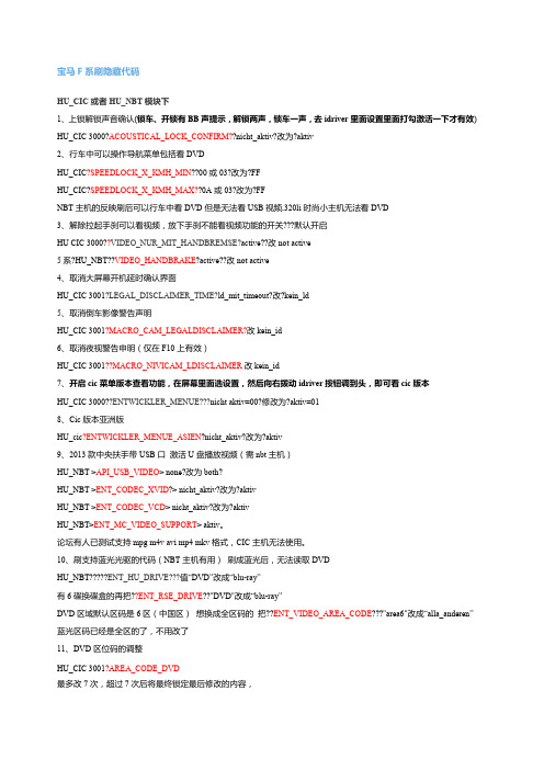
宝马F系刷隐藏代码HU_CIC或者HU_NBT模块下1、上锁解锁声音确认(锁车、开锁有BB声提示,解锁两声,锁车一声,去idriver里面设置里面打勾激活一下才有效) HU_CIC 3000?ACOUSTICAL_LOCK_CONFIRM??nicht_aktiv?改为?aktiv2、行车中可以操作导航菜单包括看DVDHU_CIC?SPEEDLOCK_X_KMH_MIN??00或03?改为?FFHU_CIC?SPEEDLOCK_X_KMH_MAX??0A或03?改为?FFNBT主机的反映刷后可以行车中看DVD但是无法看USB视频,320li时尚小主机无法看DVD3、解除拉起手刹可以看视频,放下手刹不能看视频功能的开关???默认开启HU CIC 3000??VIDEO_NUR_MIT_HANDBREMSE?active??改not active5系?HU_NBT??VIDEO_HANDBRAKE?active??改not active4、取消大屏幕开机延时确认界面HU_CIC 3001?LEGAL_DISCLAIMER_TIME?ld_mit_timeout?改?kein_ld5、取消倒车影像警告声明HU_CIC 3001?MACRO_CAM_LEGALDISCLAIMER?改kein_id6、取消夜视警告申明(仅在F10上有效)HU_CIC 3001??MACRO_NIVICAM_LDISCLAIMER改kein_id7、开启cic菜单版本查看功能,在屏幕里面选设置,然后向右拨动idriver按钮调到头,即可看cic版本HU_CIC 3000??ENTWICKLER_MENUE???nicht aktiv=00?修改为?aktiv=018、Cic版本亚洲版HU_cic?ENTWICKLER_MENUE_ASIEN?nicht_aktiv?改为?aktiv9、2013款中央扶手带USB口激活U盘播放视频(需nbt主机)HU_NBT >API_USB_VIDEO> none?改为both?HU_NBT >ENT_CODEC_XVID?> nicht_aktiv?改为?aktivHU_NBT >ENT_CODEC_VCD> nicht_aktiv?改为?aktivHU_NBT>ENT_MC_VIDEO_SUPPORT> aktiv。
F20-新宝马1系-所有刷机列表(包含跑车程序的使用方法)
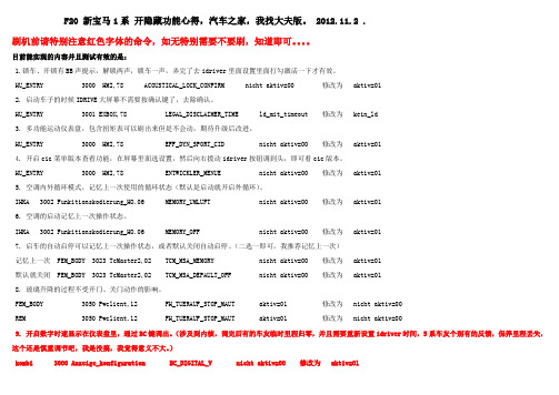
F20 新宝马1系开隐藏功能心得,汽车之家,我找大夫版。
2012.11.2 .刷机前请特别注意红色字体的命令,如无特别需要不要刷,知道即可。
目前能实现的内容并且测试有效的是:1.锁车、开锁有BB声提示,解锁两声,锁车一声,弄完了去idriver里面设置里面打勾激活一下才有效。
HU_ENTRY 3000 HMI,78 ACOUSTICAL_LOCK_CONFIRM nicht aktiv=00 修改为 aktiv=012. 启动车子的时候IDRIVE大屏幕不需要按确认键了,去除确认。
HU_ENTRY 3001 EXBOX,78 LEGAL_DISCLAIMER_TIME ld_mit_timeout 修改为 kein_ld3. 多功能运动仪表盘,包含扭矩表可以刷出来但是不会动,期待升级后改进。
HU_ENTRY 3000 HMI,78 EFF_DYN_SPORT_CID nicht aktiv=00 修改为 aktiv=014. 开启cic菜单版本查看功能,在屏幕里面选设置,然后向右拨动idriver按钮调到头,即可看cic版本。
HU_ENTRY 3000 HMI,78 ENTWICKLER_MENUE nicht aktiv=00 修改为 aktiv=015. 空调内外循环模式,记忆上一次使用的循环状态(默认是启动就开启外循环)。
IHKA 3002 Funkitionskodierung_HO.06 MEMORY_UMLUFT nicht aktiv=00 修改为 aktiv=016. 空调的启动记忆上一次操作状态。
IHKA 3002 Funkitionskodierung_HO.06 MEMORY_OFF nicht aktiv=00 修改为 aktiv=017. 启车的自动启停可以记忆上一次操作状态,或者默认关闭自动启停。
(二选一即可,我推荐记忆上一次)记忆上一次 FEM_BODY 3023 TcMaster2,02 TCM_MSA_MEMORY nicht aktiv=00 修改为 aktiv=01默认就关闭 FEM_BODY 3023 TcMaster2,02 TCM_MSA_DEPAULT_OFF nicht aktiv=00 修改为 aktiv=018. 玻璃升降的过程不受开门、关门动作的影响。
STM32固件库使用手册的中文翻译版
因为该固件库是通用的,并且包括了所有外设的功能,所以应用程序代码的大小和执行速度可能不是最优 的。对大多数应用程序来说,用户可以直接使用之,对于那些在代码大小和执行速度方面有严格要求的应 用程序,该固件库驱动程序可以作为如何设置外设的一份参考资料,根据实际需求对其进行调整。
1.3.1 变量 ................................................................................................................................................ 28 1.3.2 布尔型 ............................................................................................................................................ 28 1.3.3 标志位状态类型 ........................................................................................................................... 29 1.3.4 功能状态类型 .............................................................................................................
富士通硬盘维修全集
FUJ维修资料整理FUJ维修资料,准备打印出来备分用的。
请大家指点一下FUJITSU MPG系列的维修故障现象: 自检声正常,但系统检测不到. 这种故障是导致FUJITSU IDE硬盘身败名裂的主要原因.解决办法:1、将硬盘接入,运行相应程序。
不管出现的红色提示窗,直进到主菜单2、检查内部结构。
记下出错的模块编号。
3、选一相同FIRMWARE的正常盘,读出内部所有模块。
4、将原来发现的出错模块写回待修盘。
下次重新通电时,硬盘就可以正常认出。
富士通重写BIOS的*作步骤1、从好盘下载BIOS程序。
取一个与待修硬盘相同BIOS版本的好盘,接入后进入相应工具的菜单。
选 "DISC FIRMWARE ZONE"--"WORK WITH THE ROM"---"READ ROM TO FILE",然后输入一个文件名(易记且有特点的),回车,约10秒钟就可将该硬盘的BIOS读出并存放于指定的文件上。
2、不退出菜单,直接取下好盘,换上待写BIOS的硬盘。
当DRDY 与 DSC 指示灯亮时,表示硬盘已经准备好。
3、选菜单选 "DISC FIRMWARE ZONE"--"WORK WITH THE ROM"---"WRITE ROM FROM FILE",选择刚才指定的文件名,回车。
这个过程中硬盘自动停转,然后再次起转并自检。
约30秒钟就可完成BIOS写入。
修富士通坏区的全过程型号:FUJITSU M1636TAU 故障现象:FORMAT格式化极慢,MHDD274F查有成片的红色,绿色。
维修步骤:1,运行MHDD,多次扫描,红色,绿色无法减少。
2,运行PC3000,我是把硬盘跳为主硬盘的,不知道工厂模式如何跳,检查坏道好象没有必要跳成工厂模式!选择硬盘型号后进入主菜单,这时看到窗口上面硬盘的磁头数是2,无法修改,可能是指硬盘实际的磁头数!3,从第一个菜单开始,第一项是伺服测试:分别测试两个磁头的伺服电机速度。
惠威HR70遥控器使用说明书

HR070 Series Remote Control Programming Guide
6. Repeat steps 1 to 5 for the other components you want to control. For future reference, write down each working component code below:
HR Series Remote Control Programming
Assigned Push-button Component Program Code
TV
CBL
SAT
AUX
DVR
Push-buttons available for Programming
Flashes during Programming
4
Used to activate Programming Mode
with the most popular code first. If the component
responds, go to step 7.
6. If the component does not respond, press LEVEL+
Push-button and the Remote Control will test
The HR70 Series Remote Controls have stored in permanent memory the necessary information to send the correct commands to the component to be controlled. By entering a five digit numeric code the commands for controlling the component is activated.
NAND Flash Translation Layer (NFTL) 4.6.0

NAND Flash Translation Layer (NFTL) 4.6.0 User GuideIntroductionThis user guide describes how to implement the Micron NAND Flash Translation Layer (NFTL) software for the purpose of using a NAND Flash memory device for data storage.NFTL is a software sector manager that resides between a FAT (or sector-based) file system and Flash memory to enable Micron NAND Flash memory. The NFTL provides a small RAM/ROM footprint, consistent performance, and sector-based power loss recovery. With its user-friendly application program interface (API), Micron NFTL enables standard FAT-based file systems for Flash support. In addition, the NFTL API supports the storage of sim-ple, numerical data parameters.Nonvolatile memory such as NAND Flash can permanently store data or code without the need for a constant source of power. This capability is ideal for portable applications such as digital cameras, MP3 players, PDAs, and data storage in mobile phones. However, the Flash technology requires additional software to manage the data. For this reason, the NFTL software handles all operations required to manage embedded Flash memory devices. This eliminates the need for a developer to write additional code during the development cycle. Using this soft-ware, a developer needs only to use simple file system commands to interact with a NAND Flash memory device. The NFTL software handles all management functions so that operating systems can read and write to NAND Flash memory devices in the same way as reading and writing to disk drives. NFTL has been fully tested and debug-ged for use with a wide range of Micron NAND Flash memory devices, including single-level cell (SLC) large/small page family chips. The size of the NFTL code is around 300KB, but can vary slightly depending on the user’s config-uration.NFTL offers the best combination of Flash memory management software and NAND Flash memory devices to use in-system in consumer, automotive, mobile phone, and mass storage applications. The software minimizes the cost of embedded devices, as it allows the user to choose the most cost-effective NAND Flash memory in any density.The architecture of NFTL allows Micron NAND Flash to be easily integrated with most standard file systems. Mini-mized porting and engineering efforts helps reduce time-to-market.In addition, NFTL has a modular architecture. Each module can be changed without affecting other modules. Al-so, each module can be extracted to be used independently in a different environment. For each software module, NFTL provides functions that can be defined by the user and allows certain hardware and software features to be configured. The RAM space and the device operation settings are configured simply by changing a few lines of code.ContentsUsing NAND Flash Memory For Data Storage (4)NFTL Architecture (5)Flash Abstraction Layer (FAL) (5)Translation Module (6)Wear Leveling Module (6)Garbage Collection Module (6)Bad Block Management Module (6)Background Task Module (6)Cache Manager Module (6)Hardware Adaptation Layer (HAL) (7)Device Dependent Module (7)Platform Dependent Layer (7)Error Correction Code (ECC) Module (7)Module Interfaces (7)NFTL Software Features (9)System Requirements (11)Interface Description (12)NFTL Exported Functions (12)Enumerations, Constants, and Structures (13)API Functions (15)NFTL_Initialize Function (15)NFTL_FormatPartition Function (15)NFTL_MountPartition Function (16)NFTL_UnmountPartition Function (16)NFTL_WriteSector Function (17)NFTL_WriteSectors Function (17)NFTL_ReadSector Function (18)NFTL_DeleteSector Function (18)NFTL_DefragPartition Function (19)NFTL_GetPartitionStatus Function (20)NFTL_GetPartitionsInfo Function (20)NFTL_IsPartitionMounted Function (20)NFTL_DeInit Function (21)NFTL_StartBackground Function (21)NFTL_StopBackground Function (22)NFTL_IsBackgroundRunning Function (22)Getting Started (24)User Configuration (24)Unsupported Configurations for common.h (24)NFTL Allowed Configurations (26)Special Features (26)PL Features (26)Other Customization (26)Porting Guide (27)Integrating NFTL into a System (27)Configuring the OS Adaptation Module (27)Selecting the Correct Device Driver (28)Setting Up the NAND Platform Dependent Driver (28)Setting Up the OneNAND™ Platform Dependent Driver (29)Maximum Number of Erasable Blocks (OneNAND™ Devices Only) (30)Programming Guide (31)Normal Use of NFTL V4.6.0 (31)Step 1: Create the t_partitionInfo structure (31)Step 2: NFTL_Initialize (32)Step 3: NFTL_MountPartition (32)Step 4: Function operation (32)Step 5: NFTL_DeInit (32)Demo code for the five steps (32)First Use of NFTL V4.6.0 on a Previously-used NAND Flash Memory (35)Debug Mode Using NFTL V4.6.0 (36)Demo code (36)Definitions and Acronyms (38)Source Code Organization (40)NFTL Frequently Asked Questions (42)What are the advantages of using NFTL? (42)Does NFTL support large page (2112-byte) and small page (528-byte) NAND Flash memory devices? (42)How does NFTL manage bad blocks? (42)How many bad blocks can be managed by NFTL? (42)What is the sector size managed by NFTL? Is it possible to change it? (42)When does NFTL perform garbage collection? (42)How much RAM is required to perform NFTL data management correctly? (42)If the NAND Flash device is unformatted, is it possible to manage data storage on it through NFTL? (43)If the NAND Flash device is unformatted, is it possible to manage data storage on it through NFTL? (43)Does NFTL use error correction code (ECC)? (43)Can custom ECC hardware be used with the NFTL software? (43)Does NFTL support wear leveling? (43)Does NFTL support power loss recovery (PLR)? (43)What are the operations required to mount NFTL to a file system? (43)How much NAND physical space is accessible by the user to manage data storage (through NFTL)? (44)References (45)Revision History (46)Rev. L, 02/11 (46)Rev. K, 08/10 (46)Rev. J, 07/10 (46)Rev. 9, 03/10 (47)Rev. 8, 11/09 (47)Rev. 7, 07/09 (48)Rev. 6, 05/09 (48)Rev. 5, 04/09 (48)Rev. 4, 04/09 (48)Rev. 3, 12/08 (48)Rev. 2, 10/08 (48)Rev. 1, 03/07 (48)Disclaimer (49)Using NAND Flash Memory For Data StorageFiles in embedded file systems read and write data in small blocks called “sectors” (typi-cally 512 bytes, 1024 bytes or 2048 bytes in size). Unlike disk drives, NAND Flashmemory is not re-writable. Instead, data that is already written must be erased beforeexecuting a new Write command.NAND Flash is writable only one page at a time and it is erasable by blocks that are com-posed of pages (for more information, refer to the data sheets listed in References(page 45)). Typically, the sector size is equal to the physical page size. This means thateach erase operation involves more than one sector.To overcome the physical organization of NAND Flash devices, there are two solutionsthat can be implemented:•Use a translation layer between the file system and storage media to mask any differ-ences between Flash memory devices and traditional storage devices.•Develop a new file system that is customized for Flash device characteristics.The NAND Flash Translation Layer (NFTL) software implements the first solution.NFTL emulates the rewriting of the sectors by remapping the new write process to an-other location in the Flash memory. The previously written sector is marked “not valid”and is erased at a later time. This NFTL technique frees unusable space in the memorydevice.The “P/E cycles” are the number of possible WRITE/ERASE operations on a block. For asingle level cell (SLC) NAND device it is equal to 100,000 cycles. Functionality of thedevice beyond this threshold is not guaranteed.One of the objectives of NFTL is to guarantee that the flash medium is uniformly used.That is, each block is erased the same number of times. In addition, NFTL extracts thehardware functionality of Flash devices through a software module that manages the low-level functionality of the storage media. This module also contains software for manag-ing various possible errors during the flash operation. NFTL ensures maximum functionality and the best possible performance for all Micron Flash memory devices.NAND Flash Translation Layer (NFTL)Using NAND Flash Memory For Data StorageNFTL ArchitectureThe NFTL software, which interacts directly with the file system, consists of two layers:•Flash Abstraction Layer (FAL)•Hardware Adaptation Layer (HAL)The following figure shows how the software is used in an embedded operating system(OS) that uses NAND Flash memory for data storage.Figure 1: Design ArchitectureFlash Abstraction Layer (FAL)The Flash Abstraction Layer (FAL) provides a high-level abstraction of the physical or-ganization of NAND Flash memory devices. It emulates the rewriting of sectors in harddisks by remapping new data to another location in the memory array and marking theprevious sector invalid. The FAL contains the following modules:•Translation•Wear Leveling•Garbage Collection•Bad Block Management•Cache Manager•Background TaskIn addition, the FAL includes an algorithm that recovers the most current data when asudden power loss occurs.Translation ModuleThe Translation module, which is the primary interface in the FAL, provides the transla-tion from virtual to physical addresses and converts the logical operations into physicaloperations on the Flash memory device. It also handles the exporting of all operationsavailable on storage media (for example: write sector, read sector, and format partition). Wear Leveling ModuleIn Micron NAND Flash memory, each physical block can be programmed or erased reli-ably over 100,000 times for SLC chips. For write-intensive applications, it is recommen-ded that a wear leveling algorithm be implemented to monitor and spread the numberof PROGRAM/ERASE cycles per block.In memory devices that do not use a wear leveling algorithm, not all blocks are used atthe same rate. Blocks with long-lived, static data do not endure as many WRITE cyclesas the blocks with frequently-changed data.The Wear Leveling module ensures that the memory array is used uniformly by monitor-ing and evenly distributing the number of erase cycles per block. Each time a block isrequested by the Translation module, the Wear Leveling module allocates the least usedblock (for more information, refer to the AN1822 Wear Leveling in NAND Flash Memoryapplication note).Garbage Collection ModuleAs the FAL emulates rewriting sectors in hard disks by remapping new data to anotherlocation of the memory array and marking the previous sector invalid, eventually it maybe necessary to free some of the invalid memory space to allow further data to be writ-ten. To do this, the FAL implements the Garbage Collection module, where the validsectors are copied into a new free area and the old area is erased.The Garbage Collection module can be invoked from external modules through theTranslation Module interface (for more information, refer to the AN1821 Garbage Collec-tion in Single Level Cell NAND Flash Memory application note).Bad Block Management ModuleThe Bad Block Management module determines how to set a block as bad.Bad Blocks are blocks that contain one or more invalid bits whose reliability is not guar-anteed. Bad Blocks may be present when the device is shipped, or may develop duringthe lifetime of the device. The Bad Block Management module hides the bad blocksfrom the FAL, preventing the FAL from accessing them.Background Task ModuleNFTL's Background Task module allows the execution of garbage collection on NFTLpartitions while the system is in an idle state. This feature reduces the risk of having freespace while writing, thus improving the user's perception of system performance. Cache Manager ModuleThe Cache Manager module manages the internal data regarding the mapping of sec-tors to physical pages. It allows for faster lookups of most used sectors or all sectorsaccording to the maxCacheEntries parameter of the partition. This is achieved by reduc-ing the number of READ accesses to the device.Hardware Adaptation Layer (HAL)The Hardware Adaptation Layer (HAL) manages the hardware functions of the NANDFlash device. It defines a standard device interface, a family-dependent layer of devicedrivers (that is, NAND vs OneNAND™), and a further layer that manages platform-spe-cific hardware functionality. To increase the reliability of the system, it also implementsfeatures to manage error bits, such as error correction code (ECC). These features arenecessary because, like hard disks, the NAND Flash device may contain some invalidblocks.Device Dependent ModuleThis layer manages the differences between NAND and OneNAND™ devices. Also, it isin charge of recognizing the specific devices during run time.Platform Dependent LayerThe Platform Dependent Layer manages the platform-dependent features, includingthe support of hardware ECC. This layer is strongly customer-dependent, and as such,must be modified/updated/rewritten according to customer needs.For more information about customizing the Platform Dependent Layer, refer to Port-ing Guide (page 27).Error Correction Code (ECC) ModuleWhen digital data is stored in a memory device, it is crucial to have a mechanism thatcan detect and correct a certain number of errors. The Error Correction Code (ECC) mod-ule encodes data in such a way that it can identify and correct certain errors in the data.If the ECC does not correct the error successfully, the FAL will return a message indicat-ing that the operation has failed.The ECC code implemented in NFTL is able to correct 1-bit errors and detect 2-bit er-rors per each 512 bytes of data.Module InterfacesThe following table describes the modules and how they interact.Table 1: Module Interface InformationTable 1: Module Interface Information (Continued)NFTL Software FeaturesThe NFTL software supports the following features:•Configurable: For each software module, NFTL provides functions that can be de-fined by the user. These functions allow certain hardware and software features to beconfigured. The RAM space and device operation settings can be configured by sim-ply changing a few lines of code.•Simple integration: The NFTL architecture allows Micron NAND Flash memory devi-ces to be easily integrated with most standard file systems. It has a user-friendly APIthat supports storage of simple, numerical data parameters.Minimized porting and engineering efforts help reduce the time-to-market.•Modular architecture: NFTL has a modular architecture. Each module can bechanged without affecting other modules, or can be extracted to be used independent-ly in a different environment.•Power loss recovery (PLR): NFTL is able to recognize the system state at each power-up, even if a sudden power loss occurs. In addition, if data is corrupted, NFTLrecovers the valid data and erases the remaining data.Before using a new free block, NFTL will erase it. A write confirm called COMMIT isused to ensure that data is valid when writing the data.•Data integrity: NFTL maintains data integrity though the Bad Block Management andError Correction Code (ECC) modules.•Garbage Collection: The Garbage Collector module frees occupied NAND flash physi-cal space for disk emulation.•Garbage Collection in background: NFTL offers the capability to use the multithread-ing features of the underlying operating system to improve performance when dirtyspace must be collected and cleared. Using specific APIs, it is possible to start andstop background garbage collection while the system is up and running, and start thethread as soon as the partition has been mounted. For further customization to suitspecific needs, it is also possible to manage the thread independently per each parti-tion, allowing garbage collection in the background for one or more partitions on thedevice.•Wear leveling: NFTL guarantees uniform usage of each physical block, prolonging thedevice lifetime.•Multi block erase: This is a feature of OneNAND™. Please refer to the applicable datasheet for more information.•Operation logging: The last operation performed by NFTL is saved. This is useful forremote debugging.•Static wear leveling: Using this method, long-lived static data is copied to anotherblock so that the original block can be used for data that is changed more frequently.This is triggered when the difference between the maximum and the minimum num-ber of write cycles per block reaches a specific threshold. With this particular techni-que, the mean age of physical NAND blocks is constantly maintained.•Debug messages: Debug messages can be printed to the screen and can enabled/dis-abled for any module.•Multi-plane support: Some devices have a multi-plane feature that allows a multi de-vice operation on a block located on a different plane. Please refer to the applicabledatasheet for more details.•Bad block table: The list of bad blocks is saved in a bad block table that is stored at a location in the device.•Advanced bad block marking: NFTL adds information to bad blocks in order to store the reason the block was marked as a bad block.A bad block can be generated due to one of the following events:–Factory shipped: The block is marked as bad from the factory.–Write fail: A PROGRAM operation on a device failed. Valid data on the block issaved and the block is marked as bad.–Erase fail: A block ERASE operation failed and the block is marked as bad.–Read fail: A READ operation failed due to multiple 1-bit ECC errors.Bad blocks are marked in a field of the spare area. This field is specified in the data-sheet for each device. A block is consider bad if the value in this field does not contain 0xFFh.The following values in this field indicate the failed operation and the cause for the bad block:–BAD_BLOCK_FACTORY_SHIPPED 0x00–BAD_BLOCK_AFTER_WRITE 0x01–BAD_BLOCK_AFTER_ERASE 0x02–BAD_BLOCK_AFTER_READ 0x04•Refresh on 1-bit ECC errors: When a correctable 1-bit ECC error occurs during a READ operation, any data in the block containing the error is moved to a free block. The block in which the 1-bit error occurred is then erased.•Safe write: The combination of the define SAFE_WRITE and the field safepartition in t_partitionInfo are used to identify a safe partition. In the safe partition, a ready verify is performed for each WRITE operation. If a compare error occurs, the sector is rewrit-ten and the block is marked as a bad block.•Erase verify: A commit mark is added to erased blocks. This feature increases the pow-er loss safe level of NFTL.•Multiple partition types: NFTL supports two different types of partitions, allowing da-ta to be stored with different policies:–Standard partitions: These partitions offer the entire set of power loss recovery and data preservation features of NFTL. They can be used to store on the NAND Flash any data that must be preserved between sessions.–Swap partitions: This type of partition does not offer any data preservation between sessions or power loss recovery on data. However, it offers high READ/WRITE per-formances and can be used to store session-related data on the NAND device.System RequirementsThe size of the NFTL code depends on the user-defined configuration. However, thecode size is typically about 200KB. RAM is required to execute the NFTL code and toassist NFTL in managing storage to the NAND flash memory device.RAM usage can range from about 30KB to 80KB, depending on enabled features, config-uration, and the quantity of data written in the NAND Flash device.This RAM is used as shown below:•Approximately 20KB are used to execute the NFTL code.•Approximately 20KB are used to contain system static variables.•Approximately 26KB to 65KB are used for system dynamic variables. This space in theRAM is generally required to ensure a high throughput for each (typical usage) read/write operation.NFTL uses these RAM variables to recognize the system status and to convert logicaloperations to physical operations. As a result, NFTL does not need to access the NANDFlash.Note: The compiled code size was calculated for NFTL running on a developmentboard with a Mainstone II board running the Nucleus operating system over an x16NAND device. The sizes provided are for reference only. The code size depends on theenabled features, configuration, the processor's instruction set, and compiler optimiza-tion.Interface DescriptionNFTL manages up to 255 partitions in a single NAND device, and supports all file sys-tems that use:•512-byte sectors on SLC, small page NAND devices•2,048-byte sectors on large page SLC NAND Flash•4,096-byte sectors on large page SLC NAND flash using the multi-plane featureThe main interfaces exported by NFTL through the Translation module interface are:•Format Partition•Sector Read•Sector Write•Multiple Sector Write•Sector DeleteThe file system (FS) requirements include operation execution without knowing any spe-cific information about the selected devices. As a result:•The FAL is concerned with abstracting data to the NAND Flash architecture.•The HAL executes the operations in the NAND Flash memory.Another interface allows the file system to defragment the NAND Flash device to in-crease free space and reduce the size of the data structure that maintains the sectorhistory on the device. This operation increases the throughput and improves softwareperformance.NFTL Exported Functionsubyte NFTL_IsBackgroundRunning(ubyte)t_nftl_error NFTL_StartBackground(ubyte)t_nftl_error NFTL_StopBackground(ubyte)t_nftl_error NFTL_Initialize(ubyte,t_partitionInfo*)t_nftl_error NFTL_DeInit()t_nftl_error NFTL_FormatPartition(ubyte,uword)t_nftl_error NFTL_MountPartition(ubyte)t_nftl_error NFTL_UnmountPartition(ubyte)t_nftl_error NFTL_WriteSector(ubyte,udword,ubyte *)t_nftl_error NFTL_WriteSectors(ubyte,udword,ubyte,ubyte*)t_nftl_error NFTL_ReadSector(ubyte,udword,ubyte *)t_nftl_error NFTL_DeleteSector(ubyte,udword)t_nftl_error NFTL_DefragPartition(ubyte)t_nftl_error NFTL_GetPartitionStatus(ubyte,t_partitionStatus)t_nftl_error NFTL_GetPartitionsInfo(t_partitionStatus**)t_nftl_error NFTL_IsPartitionMounted(ubyte)Enumerations, Constants, and Structurest_nftl_errortypedef enum {/*The following values are potentially returned from NFTL APIs.*/NFTL_SUCCESS =0,NFTL_FAILURE =1,NFTL_INV ALID_PARTITION =2,NFTL_INV ALID_ADDRESS =3,NFTL_FLUSH_ERROR =5,NFTL_UNFORMATTED =6,NFTL_MOUNTED_PARTITION =0,NFTL_UNMOUNTED_PARTITION =1,NFTL_VERIFY_ERROR = 0x18,NFTL_BLANK_CHECK_FAIL = 0x20,NFTL_DISK_ERROR = 0x21,}t_nftl_error;typedef struct {ubyte number;ubyte safepartition;uword startBlock;uword sizeInBlocks;uword numOfPageInBlock;udword fillFactor;ubyte blankCheckEnabled;ubyte EnableBackground;ubyte partition_type;uword maxCacheEntries;} t_partitionInfo;t_partitionStatustypedef struct{uword freeBlocks;uword badBlocks;uword hiddenBlocks;uword occupiedBlocks;}t_partitionStatusNote: The blankCheckEnabled value must be set to 0. It will be used in future releases of NFTL.Note: For more information about these fields and structures, refer to Normal Use of NFTL V4.6.0 (page 31), Debug Mode Using NFTL V4.6.0 (page 36), and Debug Mode Using NFTL V4.6.0 (page 36).API FunctionsThe following sections provide details about each of NFTL's API functions.NFTL_Initialize FunctionThis function provides NFTL with information about the partitions that will be managed.Syntaxt_nftl_error NFTL_Initialize(ubyte partitionsNumber,t_partitionInfo *partitionInfos)ParametersReturn valuesCommentsThe number of elements in *partitionsInfo are equal to partitionsNumber. The partitions, asdefined in partitionsInfo elements, cannot overlap.NFTL_FormatPartition FunctionThis function formats a partition. This function can be used even if the partition is notmounted.Syntaxt_nftl_error NFTL_FormatPartition (ubyte partition,uword FillFactor)ParametersReturn valuesCommentspartition indicates an existing partition. FillFactor is less than partitionSize. If the formattedpartition is mounted before the format, it will be mounted after the format. Otherwise,it will remain unmounted.NFTL_MountPartition FunctionThis function mounts a formatted partition.Syntaxt_nftl_error NFTL_MountPartition (ubyte partitionNumber)ParametersReturn valuesCommentspartitionNumber indicates an existing partition. The partition must be formatted.NFTL_UnmountPartition FunctionThis function unmounts a formatted partition.Syntaxt_nftl_error NFTL_UnmountPartition (ubyte partition)ParametersReturn valuesCommentspartition indicates an existing partition. The partition must be formatted.NFTL_WriteSector FunctionThis function writes a sector.Syntaxt_nftl_error NFTL_WriteSector (ubyte partition,uword VirtualAddress,ubyte *Buffer)ParametersReturn valuesCommentsIn a SWAP partition, all written data will be lost after a power loss or power down. NFTL_WriteSectors FunctionThis function writes multiple, consecutive sectors.Syntaxt_nftl_error NFTL_WriteSectors (ubyte partition,udword VirtualAddress,ubyte numOfSectors,ubyte *Buffer)ParametersReturn valuesCommentsThe behavior of this function changes according to the partition type:•In SWAP partitions, all written data will be lost.•In non-SWAP partitions, this function manages the Power Loss Recovery sector bysector. As a result, after a power loss during WriteSectors execution, some sectors willhave been correctly updated, while others have been left as they were before the call. NFTL_ReadSector FunctionThis function reads a sector.Syntaxt_nftl_error NFTL_ReadSector (ubyte partition,udword VirtualAddress,ubyte *Buffer)ParametersReturn valuesCommentsNone.NFTL_DeleteSector FunctionThis function deletes a sector.Syntaxt_nftl_error NFTL_DeleteSector (ubyte partition,udword VirtualAddress)ParametersReturn valuesCommentsNone.NFTL_DefragPartition FunctionThis function frees invalid partition space.Syntaxt_nftl_error NFTL_DefragPartition (ubyte partition)ParametersReturn valuesCommentsNone.NFTL_GetPartitionStatus FunctionThis function returns information about a partition.Syntaxt_nftl_error NFTL_GetPartitionStatus (ubyte partition,t_partitionStatus *partitionStatus)ParametersReturn valuesCommentsNone.NFTL_GetPartitionsInfo FunctionThis function returns information about the number and type of partition.Syntaxt_nftl_error NFTL_GetPartitionsInfo (t_partitionInfo ** pinfo)ParametersReturn valuesCommentsNone.NFTL_IsPartitionMounted FunctionThis function returns the status of a partition (mounted/unmounted).Syntax。
翼虎教程

GROUP ASEDO 汽车科学教育发展机构
Automobile science education development organization
第一汽车技术服务网
/
5、修改刷出行车落锁等功能 拉动 FoCCCus 右侧的滚动条,停止到序号#32 的位置。原车数据是 01, 也就是没有行车落锁功能。 ▼
GROUP ASEDO 汽车科学教育发展机构
Automobile science education development organization
第一汽车技术服务网
/
将序号#32 后部的选择框选择为自动落锁,数值变为 02,也就是开启行车落 锁功能了。其实不论是汉化版还是英文版,大家只要记住一些功能的#XX 序号(实 际是代表字节位置)以及对应的后方的数值就可以轻松修改了。FoCCCus 数值后 的可选项可以选择为 Unknown ,此时前面的数值框会变为可修改状态,车主可以 手动输入不同的数值刷车以测试相关功能。 ▼
GROUP ASEDO 汽车科学教育发展机构
Automobile science education development organization
第一汽车技术服务网
/
2、将 ELM327 的 OBD II 插头插到主驾驶侧的 OBD II 诊断接口,并确 保接插可靠。 ▼
Automobile science education development organization
第一汽车技术服务网
/
二、刷出翼虎的隐藏功能。 (一)直接使用 FoCCCus 读取 BCM 并修改后写入 BCM 实现刷隐藏功 能。 1、将 ELM327 的 USB 插头连接到 PC 的 USB 接口。 ▼
Indradrive 系列 故障代码
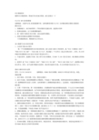
Error MessagesF9001 Error internal function call.F9002 Error internal RTOS function callF9003 WatchdogF9004 Hardware trapF8000 Fatal hardware errorF8010 Autom. commutation: Max. motion range when moving back F8011 Commutation offset could not be determinedF8012 Autom. commutation: Max. motion rangeF8013 Automatic commutation: Current too lowF8014 Automatic commutation: OvercurrentF8015 Automatic commutation: TimeoutF8016 Automatic commutation: Iteration without resultF8017 Automatic commutation: Incorrect commutation adjustment F8018 Device overtemperature shutdownF8022 Enc. 1: Enc. signals incorr. (can be cleared in ph. 2) F8023 Error mechanical link of encoder or motor connectionF8025 Overvoltage in power sectionF8027 Safe torque off while drive enabledF8028 Overcurrent in power sectionF8030 Safe stop 1 while drive enabledF8042 Encoder 2 error: Signal amplitude incorrectF8057 Device overload shutdownF8060 Overcurrent in power sectionF8064 Interruption of motor phaseF8067 Synchronization PWM-Timer wrongF8069 +/-15Volt DC errorF8070 +24Volt DC errorF8076 Error in error angle loopF8078 Speed loop error.F8079 Velocity limit value exceededF8091 Power section defectiveF8100 Error when initializing the parameter handlingF8102 Error when initializing power sectionF8118 Invalid power section/firmware combinationF8120 Invalid control section/firmware combinationF8122 Control section defectiveF8129 Incorrect optional module firmwareF8130 Firmware of option 2 of safety technology defectiveF8133 Error when checking interrupting circuitsF8134 SBS: Fatal errorF8135 SMD: Velocity exceededF8140 Fatal CCD error.F8201 Safety command for basic initialization incorrectF8203 Safety technology configuration parameter invalidF8813 Connection error mains chokeF8830 Power section errorF8838 Overcurrent external braking resistorF7010 Safely-limited increment exceededF7011 Safely-monitored position, exceeded in pos. DirectionF7012 Safely-monitored position, exceeded in neg. DirectionF7013 Safely-limited speed exceededF7020 Safe maximum speed exceededF7021 Safely-limited position exceededF7030 Position window Safe stop 2 exceededF7031 Incorrect direction of motionF7040 Validation error parameterized - effective thresholdF7041 Actual position value validation errorF7042 Validation error of safe operation modeF7043 Error of output stage interlockF7050 Time for stopping process exceeded8.3.15 F7051 Safely-monitored deceleration exceeded (159)8.4 Travel Range Errors (F6xxx) (161)8.4.1 Behavior in the Case of Travel Range Errors (161)8.4.2 F6010 PLC Runtime Error (162)8.4.3 F6024 Maximum braking time exceeded (163)8.4.4 F6028 Position limit value exceeded (overflow) (164)8.4.5 F6029 Positive position limit exceeded (164)8.4.6 F6030 Negative position limit exceeded (165)8.4.7 F6034 Emergency-Stop (166)8.4.8 F6042 Both travel range limit switches activated (167)8.4.9 F6043 Positive travel range limit switch activated (167)8.4.10 F6044 Negative travel range limit switch activated (168)8.4.11 F6140 CCD slave error (emergency halt) (169)8.5 Interface Errors (F4xxx) (169)8.5.1 Behavior in the Case of Interface Errors (169)8.5.2 F4001 Sync telegram failure (170)8.5.3 F4002 RTD telegram failure (171)8.5.4 F4003 Invalid communication phase shutdown (172)8.5.5 F4004 Error during phase progression (172)8.5.6 F4005 Error during phase regression (173)8.5.7 F4006 Phase switching without ready signal (173)8.5.8 F4009 Bus failure (173)8.5.9 F4012 Incorrect I/O length (175)8.5.10 F4016 PLC double real-time channel failure (176)8.5.11 F4017 S-III: Incorrect sequence during phase switch (176)8.5.12 F4034 Emergency-Stop (177)8.5.13 F4140 CCD communication error (178)8.6 Non-Fatal Safety Technology Errors (F3xxx) (178)8.6.1 Behavior in the Case of Non-Fatal Safety Technology Errors (178)8.6.2 F3111 Refer. missing when selecting safety related end pos (179)8.6.3 F3112 Safe reference missing (179)8.6.4 F3115 Brake check time interval exceeded (181)Troubleshooting Guide | Rexroth IndraDrive Electric Drivesand ControlsI Bosch Rexroth AG VII/XXIITable of ContentsPage8.6.5 F3116 Nominal load torque of holding system exceeded (182)8.6.6 F3117 Actual position values validation error (182)8.6.7 F3122 SBS: System error (183)8.6.8 F3123 SBS: Brake check missing (184)8.6.9 F3130 Error when checking input signals (185)8.6.10 F3131 Error when checking acknowledgment signal (185)8.6.11 F3132 Error when checking diagnostic output signal (186)8.6.12 F3133 Error when checking interrupting circuits (187)8.6.13 F3134 Dynamization time interval incorrect (188)8.6.14 F3135 Dynamization pulse width incorrect (189)8.6.15 F3140 Safety parameters validation error (192)8.6.16 F3141 Selection validation error (192)8.6.17 F3142 Activation time of enabling control exceeded (193)8.6.18 F3143 Safety command for clearing errors incorrect (194)8.6.19 F3144 Incorrect safety configuration (195)8.6.20 F3145 Error when unlocking the safety door (196)8.6.21 F3146 System error channel 2 (197)8.6.22 F3147 System error channel 1 (198)8.6.23 F3150 Safety command for system start incorrect (199)8.6.24 F3151 Safety command for system halt incorrect (200)8.6.25 F3152 Incorrect backup of safety technology data (201)8.6.26 F3160 Communication error of safe communication (202)8.7 Non-Fatal Errors (F2xxx) (202)8.7.1 Behavior in the Case of Non-Fatal Errors (202)8.7.2 F2002 Encoder assignment not allowed for synchronization (203)8.7.3 F2003 Motion step skipped (203)8.7.4 F2004 Error in MotionProfile (204)8.7.5 F2005 Cam table invalid (205)8.7.6 F2006 MMC was removed (206)8.7.7 F2007 Switching to non-initialized operation mode (206)8.7.8 F2008 RL The motor type has changed (207)8.7.9 F2009 PL Load parameter default values (208)8.7.10 F2010 Error when initializing digital I/O (-> S-0-0423) (209)8.7.11 F2011 PLC - Error no. 1 (210)8.7.12 F2012 PLC - Error no. 2 (210)8.7.13 F2013 PLC - Error no. 3 (211)8.7.14 F2014 PLC - Error no. 4 (211)8.7.15 F2018 Device overtemperature shutdown (211)8.7.16 F2019 Motor overtemperature shutdown (212)8.7.17 F2021 Motor temperature monitor defective (213)8.7.18 F2022 Device temperature monitor defective (214)8.7.19 F2025 Drive not ready for control (214)8.7.20 F2026 Undervoltage in power section (215)8.7.21 F2027 Excessive oscillation in DC bus (216)8.7.22 F2028 Excessive deviation (216)8.7.23 F2031 Encoder 1 error: Signal amplitude incorrect (217)VIII/XXII Bosch Rexroth AG | Electric Drivesand ControlsRexroth IndraDrive | Troubleshooting GuideTable of ContentsPage8.7.24 F2032 Validation error during commutation fine adjustment (217)8.7.25 F2033 External power supply X10 error (218)8.7.26 F2036 Excessive position feedback difference (219)8.7.27 F2037 Excessive position command difference (220)8.7.28 F2039 Maximum acceleration exceeded (220)8.7.29 F2040 Device overtemperature 2 shutdown (221)8.7.30 F2042 Encoder 2: Encoder signals incorrect (222)8.7.31 F2043 Measuring encoder: Encoder signals incorrect (222)8.7.32 F2044 External power supply X15 error (223)8.7.33 F2048 Low battery voltage (224)8.7.34 F2050 Overflow of target position preset memory (225)8.7.35 F2051 No sequential block in target position preset memory (225)8.7.36 F2053 Incr. encoder emulator: Pulse frequency too high (226)8.7.37 F2054 Incr. encoder emulator: Hardware error (226)8.7.38 F2055 External power supply dig. I/O error (227)8.7.39 F2057 Target position out of travel range (227)8.7.40 F2058 Internal overflow by positioning input (228)8.7.41 F2059 Incorrect command value direction when positioning (229)8.7.42 F2063 Internal overflow master axis generator (230)8.7.43 F2064 Incorrect cmd value direction master axis generator (230)8.7.44 F2067 Synchronization to master communication incorrect (231)8.7.45 F2068 Brake error (231)8.7.46 F2069 Error when releasing the motor holding brake (232)8.7.47 F2074 Actual pos. value 1 outside absolute encoder window (232)8.7.48 F2075 Actual pos. value 2 outside absolute encoder window (233)8.7.49 F2076 Actual pos. value 3 outside absolute encoder window (234)8.7.50 F2077 Current measurement trim wrong (235)8.7.51 F2086 Error supply module (236)8.7.52 F2087 Module group communication error (236)8.7.53 F2100 Incorrect access to command value memory (237)8.7.54 F2101 It was impossible to address MMC (237)8.7.55 F2102 It was impossible to address I2C memory (238)8.7.56 F2103 It was impossible to address EnDat memory (238)8.7.57 F2104 Commutation offset invalid (239)8.7.58 F2105 It was impossible to address Hiperface memory (239)8.7.59 F2110 Error in non-cyclical data communic. of power section (240)8.7.60 F2120 MMC: Defective or missing, replace (240)8.7.61 F2121 MMC: Incorrect data or file, create correctly (241)8.7.62 F2122 MMC: Incorrect IBF file, correct it (241)8.7.63 F2123 Retain data backup impossible (242)8.7.64 F2124 MMC: Saving too slowly, replace (243)8.7.65 F2130 Error comfort control panel (243)8.7.66 F2140 CCD slave error (243)8.7.67 F2150 MLD motion function block error (244)8.7.68 F2174 Loss of motor encoder reference (244)8.7.69 F2175 Loss of optional encoder reference (245)Troubleshooting Guide | Rexroth IndraDrive Electric Drivesand Controls| Bosch Rexroth AG IX/XXIITable of ContentsPage8.7.70 F2176 Loss of measuring encoder reference (246)8.7.71 F2177 Modulo limitation error of motor encoder (246)8.7.72 F2178 Modulo limitation error of optional encoder (247)8.7.73 F2179 Modulo limitation error of measuring encoder (247)8.7.74 F2190 Incorrect Ethernet configuration (248)8.7.75 F2260 Command current limit shutoff (249)8.7.76 F2270 Analog input 1 or 2, wire break (249)8.7.77 F2802 PLL is not synchronized (250)8.7.78 F2814 Undervoltage in mains (250)8.7.79 F2815 Overvoltage in mains (251)8.7.80 F2816 Softstart fault power supply unit (251)8.7.81 F2817 Overvoltage in power section (251)8.7.82 F2818 Phase failure (252)8.7.83 F2819 Mains failure (253)8.7.84 F2820 Braking resistor overload (253)8.7.85 F2821 Error in control of braking resistor (254)8.7.86 F2825 Switch-on threshold braking resistor too low (255)8.7.87 F2833 Ground fault in motor line (255)8.7.88 F2834 Contactor control error (256)8.7.89 F2835 Mains contactor wiring error (256)8.7.90 F2836 DC bus balancing monitor error (257)8.7.91 F2837 Contactor monitoring error (257)8.7.92 F2840 Error supply shutdown (257)8.7.93 F2860 Overcurrent in mains-side power section (258)8.7.94 F2890 Invalid device code (259)8.7.95 F2891 Incorrect interrupt timing (259)8.7.96 F2892 Hardware variant not supported (259)8.8 SERCOS Error Codes / Error Messages of Serial Communication (259)9 Warnings (Exxxx) (263)9.1 Fatal Warnings (E8xxx) (263)9.1.1 Behavior in the Case of Fatal Warnings (263)9.1.2 E8025 Overvoltage in power section (263)9.1.3 E8026 Undervoltage in power section (264)9.1.4 E8027 Safe torque off while drive enabled (265)9.1.5 E8028 Overcurrent in power section (265)9.1.6 E8029 Positive position limit exceeded (266)9.1.7 E8030 Negative position limit exceeded (267)9.1.8 E8034 Emergency-Stop (268)9.1.9 E8040 Torque/force actual value limit active (268)9.1.10 E8041 Current limit active (269)9.1.11 E8042 Both travel range limit switches activated (269)9.1.12 E8043 Positive travel range limit switch activated (270)9.1.13 E8044 Negative travel range limit switch activated (271)9.1.14 E8055 Motor overload, current limit active (271)9.1.15 E8057 Device overload, current limit active (272)X/XXII Bosch Rexroth AG | Electric Drivesand ControlsRexroth IndraDrive | Troubleshooting GuideTable of ContentsPage9.1.16 E8058 Drive system not ready for operation (273)9.1.17 E8260 Torque/force command value limit active (273)9.1.18 E8802 PLL is not synchronized (274)9.1.19 E8814 Undervoltage in mains (275)9.1.20 E8815 Overvoltage in mains (275)9.1.21 E8818 Phase failure (276)9.1.22 E8819 Mains failure (276)9.2 Warnings of Category E4xxx (277)9.2.1 E4001 Double MST failure shutdown (277)9.2.2 E4002 Double MDT failure shutdown (278)9.2.3 E4005 No command value input via master communication (279)9.2.4 E4007 SERCOS III: Consumer connection failed (280)9.2.5 E4008 Invalid addressing command value data container A (280)9.2.6 E4009 Invalid addressing actual value data container A (281)9.2.7 E4010 Slave not scanned or address 0 (281)9.2.8 E4012 Maximum number of CCD slaves exceeded (282)9.2.9 E4013 Incorrect CCD addressing (282)9.2.10 E4014 Incorrect phase switch of CCD slaves (283)9.3 Possible Warnings When Operating Safety Technology (E3xxx) (283)9.3.1 Behavior in Case a Safety Technology Warning Occurs (283)9.3.2 E3100 Error when checking input signals (284)9.3.3 E3101 Error when checking acknowledgment signal (284)9.3.4 E3102 Actual position values validation error (285)9.3.5 E3103 Dynamization failed (285)9.3.6 E3104 Safety parameters validation error (286)9.3.7 E3105 Validation error of safe operation mode (286)9.3.8 E3106 System error safety technology (287)9.3.9 E3107 Safe reference missing (287)9.3.10 E3108 Safely-monitored deceleration exceeded (288)9.3.11 E3110 Time interval of forced dynamization exceeded (289)9.3.12 E3115 Prewarning, end of brake check time interval (289)9.3.13 E3116 Nominal load torque of holding system reached (290)9.4 Non-Fatal Warnings (E2xxx) (290)9.4.1 Behavior in Case a Non-Fatal Warning Occurs (290)9.4.2 E2010 Position control with encoder 2 not possible (291)9.4.3 E2011 PLC - Warning no. 1 (291)9.4.4 E2012 PLC - Warning no. 2 (291)9.4.5 E2013 PLC - Warning no. 3 (292)9.4.6 E2014 PLC - Warning no. 4 (292)9.4.7 E2021 Motor temperature outside of measuring range (292)9.4.8 E2026 Undervoltage in power section (293)9.4.9 E2040 Device overtemperature 2 prewarning (294)9.4.10 E2047 Interpolation velocity = 0 (294)9.4.11 E2048 Interpolation acceleration = 0 (295)9.4.12 E2049 Positioning velocity >= limit value (296)9.4.13 E2050 Device overtemp. Prewarning (297)Troubleshooting Guide | Rexroth IndraDrive Electric Drivesand Controls| Bosch Rexroth AG XI/XXIITable of ContentsPage9.4.14 E2051 Motor overtemp. prewarning (298)9.4.15 E2053 Target position out of travel range (298)9.4.16 E2054 Not homed (300)9.4.17 E2055 Feedrate override S-0-0108 = 0 (300)9.4.18 E2056 Torque limit = 0 (301)9.4.19 E2058 Selected positioning block has not been programmed (302)9.4.20 E2059 Velocity command value limit active (302)9.4.21 E2061 Device overload prewarning (303)9.4.22 E2063 Velocity command value > limit value (304)9.4.23 E2064 Target position out of num. range (304)9.4.24 E2069 Holding brake torque too low (305)9.4.25 E2070 Acceleration limit active (306)9.4.26 E2074 Encoder 1: Encoder signals disturbed (306)9.4.27 E2075 Encoder 2: Encoder signals disturbed (307)9.4.28 E2076 Measuring encoder: Encoder signals disturbed (308)9.4.29 E2077 Absolute encoder monitoring, motor encoder (encoder alarm) (308)9.4.30 E2078 Absolute encoder monitoring, opt. encoder (encoder alarm) (309)9.4.31 E2079 Absolute enc. monitoring, measuring encoder (encoder alarm) (309)9.4.32 E2086 Prewarning supply module overload (310)9.4.33 E2092 Internal synchronization defective (310)9.4.34 E2100 Positioning velocity of master axis generator too high (311)9.4.35 E2101 Acceleration of master axis generator is zero (312)9.4.36 E2140 CCD error at node (312)9.4.37 E2270 Analog input 1 or 2, wire break (312)9.4.38 E2802 HW control of braking resistor (313)9.4.39 E2810 Drive system not ready for operation (314)9.4.40 E2814 Undervoltage in mains (314)9.4.41 E2816 Undervoltage in power section (314)9.4.42 E2818 Phase failure (315)9.4.43 E2819 Mains failure (315)9.4.44 E2820 Braking resistor overload prewarning (316)9.4.45 E2829 Not ready for power on (316)。
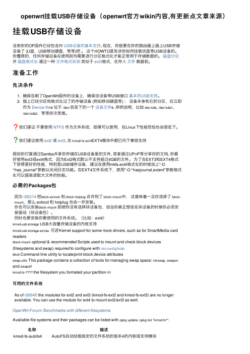
openwrt挂载USB存储设备(openwrt官方wikin内容,有更新点文章来源)
openwrt挂载USB存储设备(openwrt官⽅wikin内容,有更新点⽂章来源)挂载USB存储设备设若你的OP固件已经包含对USB设备的基本⽀持, 现在,你就要在你的路由器上插上USB存储设备了 (U盘,USB移动硬盘,等等)吧。
这个HOWTO是告诉你如何挂载优盘等USB设备的。
你懂得的,任何存储设备在使⽤前均需要进⾏分区格式化才能正常⽤于存储数据的。
磁盘分区并磁盘格式化通过⼀种⽂件格式系统类似于ext3格式,在存⼊⽂件数据前。
准备⼯作先决条件1. 确保在刷了OpenWrt固件的设备上,确保该设备带USB接⼝基本的USB⽀持。
2. 插上已经分区和格式化过了的存储设备 (例如移动硬盘等) ;设备本⾝和它的分区,应⽴即作为Device file s 位于/dev/⽬录下的⼀个设备⽂件s ,举例说明,⽐如dev/sda, /dev/sda1,/dev/sda2,等等依次类推。
我们建议不要使⽤NTFS作为⽂件系统,即便可以使⽤,在Linux下性能恐怕也会很低下。
我们建议使⽤ext2或ext3, 在kmod-fs-ext4EXT4模块中都已向下兼容⽀持假如你打算通过Samba共享你存储在USB设备⾥的⽂件, 或者通过UPnP等分享你的⽂档, 你最好使⽤ext3或ext4格式,因为Ext2格式默认不⽀持超过4GB的⽂件。
为了在EXT3和EXT4格式下获得更好的性能,特别是USB储存设备,建议在使⽤mkfs.ext4格式化的时候加上"-O^has_journal"参数以关闭⽇志功能。
在EXT4⽂件系统下,使⽤"-O ^hasjournal,extent"参数格式化可以提⾼读取⼤⽂件的性能。
必需的Packages包因为r26314把block-extroot和block-hotplug合并到了block-mount中,这意味着⼀旦你选择了block-mount,那么 extroot 和 hotplug 也会⼀并安装。
广州本田雅阁“check engine”灯亮

广州本田雅阁2.3L轿车“CHECK ENGINE”异常亮起故障现象:一辆广州本田雅阁2.3L轿车,故障灯“CHECK ENGINE”异常亮起。
故障排除:用故障指示灯(MIL)显示故障诊断代码(DTC)为21,含义为VTEC电磁阀电路有故障。
该发动机型号为F23A3,SOHC电子控制程序多点燃油喷射,且配置三元催化转化器。
该发动机装备有可变气门正时和气门开度系统VTEC,其目的是用来改善低转速时发动机扭力和高转速的功率。
VTEC系统的传动机构如图 1所示。
推动中央摇臂、主摇臂、副摇臂的3个凸轮高低依次减小。
在发动机低转速时,主进气门以正常的开度动作,副进气门只以微小的开度动作,防止燃油堆积在进气门口处。
而主副进气门开度的差距是为了使进入气缸的混合气产生涡流,以达到最低的油耗而有最高的动力输出;在高转速时,正时活塞被油压推动如图 2所示,再推动两个活塞同步移动,从而使3个摇臂接合为一,并由中央凸轮推动,进而使主副进气门有更大的开度,发动机产生更大的功率。
VTEC系统是由发动机电脑根据转速信号、车速信号、水温信号和发动机负荷信号进行控制。
当发动机转速在4800r/min以上,车速达20Km/h以上,水温在60℃以上,且发动机进气为负压等条件时,主电脑B12输出12V电压,如图 3所示,使位于气门室罩左后方的液压管道控制电磁阀打开,让油压作用在VTEC系统的传动机构上,从而增加进气门开启行程。
电磁阀线圈的内部电阻为14-30Ω。
若该电磁阀及其线路不良,就会产生发动机故障代码21。
电磁阀下方的油压开关,通过油压信号来监测电磁阀是否动作,如图 4所示。
若电磁阀不打开,则压力开关的电阻值为0Ω。
此车的情况是,在高速行驶后恢复怠速状态,电磁阀仍有12V 电压,意即压力开关仍处于断开状态,于是发动机电脑判定VTEC系统有故障。
检查压力开关线路,有12V电压输出及负极回路搭铁良好,说明问题在压力开关本身工作不良。
潍柴汽车产品说明书

I
INDEX
v w
Main Menu
Index
Changing Oil How to......................................... 147 When to...................................Байду номын сангаас... 135
Charging System Indicator .... 46, 186 Checklist, Before Driving............. 123 Child Safety ...................................... 29
Booster Seats ............................... 38 Child Seats.................................... 34 Important Safety Reminders ...... 32 Larger Children ........................... 37 Risk with Airbags ........................ 30 Small Children.............................. 33 Child Seats........................................ 34 Cleaning Seat Belts........................ 160 Clock.................................................. 54 Clutch Fluid.................................... 154 CO in the Exhaust ......................... 207 Cold Weather, Starting in ............. 124 Compact Spare Tire....................... 174 Consumer Informationˎ................ 212 Controls, Instruments and.............. 43 Convertible Top ............................... 70 Convertible Top Cover................ 72 Lowering the Convertible Top... 70 Maintenance................................. 74 Raising the Convertible Top ...... 73
悍马汽车部件维修指南说明书

Cutoff Indicator Works........... 49
How Your Front Airbags Work.......................................... 46
CONTINUED
I
v w
Main Menu
Index
Bulb Replacement Back-up Lights ........................... 206 Stop Light ................................... 206 Cargo Area Light ....................... 211 Front Parking Lights................. 205 Front Side Marker Lights......... 204 Headlights .................................. 202 High-mount Brake Light .......... 207 Interior Lights............................ 210 License Plate Lights.................. 209 Side Marker Lights ................... 204 Side Turn Signal Lights ............ 208 Specifications ............................. 251 Turn Signal Lights..................... 203
Atmel SMART SAMA5D4系列720p硬件视频解码器和高级安全密钥应用说明书

Key Applications• Control panels for security, home automation, thermostats, etc.• Surveillance cameras• Industrial human-machine interface (HMI)• Fitness equipment, such as treadmills and exercise machines • Industrial and residential gateways •Smart grid infrastructureThe new Atmel ® | SMART SAMA5D4 series, expands the SAMA5 microprocessors family and targets IoT, Industrial and Consumer applications. It is ARM ® Cortex ®-A5-based, and adds a 720p resolution hardware video decoder and advanced security features. The chip has significantly better system performance using the ARM NEON ™ 128-bit SIMD (single instruction, multiple data) architecture extension and a 128kByte L2 Cache. The IC has advanced security features to protect the application software from counterfeiting, to safeguard software assets, and to securely store and transfer data.Key Highlights720p 30fps Video PlaybackThe SAMA5D4 series enables you to bring up to 720p 30fps video playback to your user interface applications using theembedded hardware video decoder that supports H264, VP8, MPEG4, and JPEG. This is complemented by an integrated TFT LCD display controller and resistive touchscreen interface.High-performance ArchitectureBased on the ARM Cortex-A5 core with the ARM NEON SIMD engine, the SAMA5D4 series is ideal for applications requiring high-precision computing and fast signal processing. This series of microprocessors delivers 945DMIPS at 600MHz and a 128kB of L2 cache improves the overall system performance. The SAMA5D4 also features a 32-bit wide DDR controller running up to 200MHz that can deliver up to 1408MB/s of bandwidth. It is configurable in either a 16- or 32-bit bus interface allowing you an optimum trade-off between performance and memory cost.Advanced SecurityThe SAMA5D4 series security features prevent cloning of your application, protects and authenticates software, and securely stores and transfer data. It allows unique on-the-fly encryption and decryption of software code from the external DRAM, and includes secure boot, tamper detection pins, and safe erasure of security-critical data. The part features the ARM TrustZone ® system-wide approach to security as well as advanced hardware encryption engines supporting private and public key cryptography.Lifetime CommitmentAtmel offers customers a 12-years lifetime commitment from the time of this product’s introduction.Memory Connectivity User Interface User Interface System SecurityControl User Interface42-ch DMADDR2, LPDDR, LPDDR2Controller 3 HS/FS/LS USB ports 3 Host or 2 Host +1 Device2 EMAC 10/100w/ IEEE15882 HS SDIO/SD/MMC 8 UART, 8 SPI ,4 TWI, Soft modemTFT LCD Controller with Overlays720p Video Decoder Camera Interface,2 I2SResistive TouchscreenController2 RC OSC, 2 xtal OSC, 2 PLL, Voltage Regulator Watchdog, POR, RTC Backup unit with8 kb SRAMRSA, ECC co-processor 3DES, AES, SHA, TRNGOn the fly DDR Encryption/Decryption 8x Tamper Pins, Secure Boot5-ch 10-bit ADC 4 x 16-bit PWM 9 x 32-bit Timers152 IOsSLC/MLC NAND Controllerwith 24-bit ECC External Bus Interface128 kb SRAM BootROM 512 Fuse Bits64-bit AXI/AHBCortex ®-A5SAMA5D4600 MHz2x32 kb L1 Cache 128 kb L2 CacheAtmel Corporation 1600 Technology Drive, San Jose, CA 95110 USA T : (+1)(408) 441. 0311 F : (+1)(408) 436. 4200 | © 2015 Atmel Corporation. / Rev.: Atmel-45090B-SAMA5D4_E_US_092015Atmel,® Atmel logo and combinations thereof, Enabling Unlimited Possibilities,® and others are registered trademarks or trademarks of Atmel Corporation in U. S. and other countries. ARM,® ARM Connected ® logo and others are the registered trademarks or trademarks of ARM Ltd. Other terms and product names may be trademarks of others.Disclaimer: The information in this document is provided in connection with Atmel products. No license, express or implied, by estoppel or otherwise, to any intellectual property right is granted by this document or in connection with the sale of Atmel products. EXCEPT AS SET FORTH IN THE ATMEL TERMS AND CONDITIONS OF SALES LOCATED ON THE ATMEL WEBSITE, ATMEL ASSUMES NO LIABILITY WHATSOEVER AND DISCLAIMS ANY EXPRESS, IMPLIED OR STATUTORY WARRANTY RE-LATING TO ITS PRODUCTS INCLUDING, BUT NOT LIMITED TO, THE IMPLIED WARRANTY OF MERCHANTABILITY, FITNESS FOR A PARTICULAR PURPOSE, OR NON-INFRINGEMENT. IN NO EVENT SHALL ATMEL BE LIABLE FOR ANY DIRECT, INDIRECT, CONSEQUENTIAL, PUNITIVE, SPECIAL OR INCIDENTAL DAMAGES (INCLUDING, WITHOUT LIMITATION, DAMAGES FOR LOSS AND PROFITS, BUSINESS INTERRUPTION, OR LOSS OF INFORMATION) ARISING OUT OF THE USE OR INABILITY TO USE THIS DOCUMENT, EVEN IF ATMEL HAS BEEN ADVISED OF THE POSSIBILITY OF SUCH DAMAGES. Atmel makes no representations or warranties with respect to the accuracy or completeness of the contents of this document and reserves the right to make changes to specifications and products descriptions at any time without notice. Atmel does not make any commitment to update the information contained herein. Unless specifically provided otherwise, Atmel products are not suitable for, and shallnot be used in, automotive applications. Atmel products are not intended, authorized, or warranted for use as components in applications intended to support or sustain life.EcosystemAtmel has created and supports a free Linux ® distributions available at and https:///linux4sam . With our commitment to the Linux open-source community, we provide full coverage of SoC peripherals in the Linux kernel as well as bootloaders such as AT91Bootstrap and U-Boot.Atmel offers a free graphics software development kit (SDK) based on Qt available at . This SDK includes demos, widgets, backgound images, a set of icons, and useful graphical elements. Using these proven elements, you can develop your own customized user interface.Atmel is now offering a free Android ™ port for the SAMA5D devices, available at /android4sam . Originally developed for mobile handset devices, Android is ideal for use in embedded applications such as control panels, smart watches, DECT phones, and more. Android comes with multimedia and connectivity stacks, graphical user interfaces and a comprehensive SDK.For RTOS, bare metal C or C++ designers, Atmel delivers the softpack, a set of around 40 C drivers that run on the SAMA5D4 evaluation kits and exercises all peripherals. The softpack is also very useful for board bring up as well asquick prototyping and available for download from the product page on the Atmel web site.All devices are -40°C to +85°C temperature range.* Security: On the fly encryption/decryption of DRAM, secure boot, tamper detection pins, secure key storage, ARM Trust Zone, hardware cryptography engines RSA, ECC, AES, 3DES as well as SHA and TRNGTo evaluate and prototype your application, Atmel provides a low cost evaluation kit. To ease your design process and reduce your time-to-market, Atmel collaborates with a global and expanding network of partners that deliver hardware, PMIC, memories, SOM (system-on-module), and software solution for the SAMA5D4 series of MPUs. For more information on our partners and the Atmel evaluation kit, you can visit /microsite/SAMA5SAMA5D4 Series Selector GuideFor more information on the SAMA5D4 series, go to /SAMA5D4。
linuxdmesg查看系统故障信息

linuxdmesg查看系统故障信息dmesg 可以查看linux 内核信息dmesg’命令设备故障的诊断是⾮常重要的。
在‘dmesg’命令的帮助下进⾏硬件的连接或断开连接操作时,我们可以看到硬件的检测或者断开连接的信息。
‘dmesg’命令在多数基于Linux和Unix的操作系统中都可以使⽤。
1. 列出加载到内核中的所有驱动我们可以使⽤如‘more’。
‘tail’, ‘less ’或者‘grep’⽂字处理⼯具来处理‘dmesg’命令的输出。
由于dmesg⽇志的输出不适合在⼀页中完全显⽰,因此我们使⽤管道(pipe)将其输出送到more或者less命令单页显⽰。
root@cdncenter ~]# dmesg |more[ 0.000000] Initializing cgroup subsys cpuset[ 0.000000] Initializing cgroup subsys cpu[ 0.000000] Initializing cgroup subsys cpuacct[ 0.000000] Linux version 3.10.0-693.2.2.el7.x86_64 (builder@) (gcc version 4.8.520150623(Red Hat 4.8.5-16) (GCC) ) #1 SMP Tue Sep 1222:26:13 UTC 2017[ 0.000000] Command line: BOOT_IMAGE=/boot/vmlinuz-3.10.0-693.2.2.el7.x86_64 root=UUID=eb448abb-3012-4d8d-bcde-94434d586a31 ro crashkernel=auto net.ifnames=0 console=tty0 console=ttyS0,115200n8[ 0.000000] e820: BIOS-provided physical RAM map:[ 0.000000] BIOS-e820: [mem 0x0000000000000000-0x000000000009fbff] usable[ 0.000000] BIOS-e820: [mem 0x000000000009fc00-0x000000000009ffff] reserved[ 0.000000] BIOS-e820: [mem 0x00000000000f0000-0x00000000000fffff] reserved[ 0.000000] BIOS-e820: [mem 0x0000000000100000-0x00000000bffdffff] usable[ 0.000000] BIOS-e820: [mem 0x00000000bffe0000-0x00000000bfffffff] reserved[ 0.000000] BIOS-e820: [mem 0x00000000feffc000-0x00000000feffffff] reserved[ 0.000000] BIOS-e820: [mem 0x00000000fffc0000-0x00000000ffffffff] reserved[ 0.000000] BIOS-e820: [mem 0x0000000100000000-0x000000043fffffff] usable[ 0.000000] NX (Execute Disable) protection: active[ 0.000000] SMBIOS 2.8 present.[ 0.000000] DMI: Alibaba Cloud Alibaba Cloud ECS, BIOS rel-1.7.5-0-ge51488c-20140602_ 04/01/2014[ 0.000000] Hypervisor detected: KVM[ 0.000000] e820: update [mem 0x00000000-0x00000fff] usable ==> reserved[ 0.000000] e820: remove [mem 0x000a0000-0x000fffff] usable[ 0.000000] e820: last_pfn = 0x440000 max_arch_pfn = 0x400000000[ 0.000000] MTRR default type: write-back[ 0.000000] MTRR fixed ranges enabled:[ 0.000000] 00000-9FFFF write-back[ 0.000000] A0000-BFFFF uncachable[ 0.000000] C0000-FFFFF write-protect[ 0.000000] MTRR variable ranges enabled:[ 0.000000] 0 base 0000C0000000 mask 3FFFC0000000 uncachable[ 0.000000] 1 disabled[ 0.000000] 2 disabled[ 0.000000] 3 disabled[ 0.000000] 4 disabled[ 0.000000] 5 disabled[ 0.000000] 6 disabled[ 0.000000] 7 disabled[ 0.000000] x86 PAT enabled: cpu 0, old 0x7040600070406, new 0x7010600070106[ 0.000000] e820: last_pfn = 0xbffe0 max_arch_pfn = 0x400000000[ 0.000000] found SMP MP-table at [mem 0x000f0e80-0x000f0e8f] mapped at [ffff8800000f0e80][ 0.000000] Base memory trampoline at [ffff880000099000] 99000 size 24576[ 0.000000] Using GB pages for direct mapping[ 0.000000] BRK [0x01fe9000, 0x01fe9fff] PGTABLE[ 0.000000] BRK [0x01fea000, 0x01feafff] PGTABLE[ 0.000000] BRK [0x01feb000, 0x01febfff] PGTABLE[ 0.000000] RAMDISK: [mem 0x35e41000-0x36f18fff]--More--dmesg | less2. 列出所有被检测到的硬件要显⽰所有被内核检测到的硬盘设备,你可以使⽤‘grep’命令搜索‘sda’关键词,如下dmesg |grep sdasd 0:1:0:0: [sda] 584843264512-byte logical blocks: (299 GB/278 GiB)sd 0:1:0:0: [sda] Write Protect is offsd 0:1:0:0: [sda] Mode Sense: 03000008sd 0:1:0:0: [sda] Write cache: disabled, read cache: enabled, doesn't support DPO or FUAsda: sda1 sda2 sda3 sda4 < sda5 sda6 sda7 sda8 >sd 0:1:0:0: [sda] Attached SCSI diskEXT4-fs (sda5): INFO: recovery required on readonly filesystemEXT4-fs (sda5): write access will be enabled during recoveryEXT4-fs (sda5): orphan cleanup on readonly fsEXT4-fs (sda5): ext4_orphan_cleanup: deleting unreferenced inode 128070EXT4-fs (sda5): ext4_orphan_cleanup: deleting unreferenced inode 128092EXT4-fs (sda5): ext4_orphan_cleanup: deleting unreferenced inode 128051EXT4-fs (sda5): ext4_orphan_cleanup: deleting unreferenced inode 129385EXT4-fs (sda5): ext4_orphan_cleanup: deleting unreferenced inode 128052EXT4-fs (sda5): ext4_orphan_cleanup: deleting unreferenced inode 128373EXT4-fs (sda5): ext4_orphan_cleanup: deleting unreferenced inode 128049EXT4-fs (sda5): ext4_orphan_cleanup: deleting unreferenced inode 128046EXT4-fs (sda5): ext4_orphan_cleanup: deleting unreferenced inode 128039EXT4-fs (sda5): ext4_orphan_cleanup: deleting unreferenced inode 128038EXT4-fs (sda5): ext4_orphan_cleanup: deleting unreferenced inode 128014EXT4-fs (sda5): 11 orphan inodes deletedEXT4-fs (sda5): recovery completeEXT4-fs (sda5): mounted filesystem with ordered data mode. Opts:dracut: Mounted root filesystem /dev/sda5EXT4-fs (sda1): mounted filesystem with ordered data mode. Opts:EXT4-fs (sda8): mounted filesystem with ordered data mode. Opts:EXT4-fs (sda6): mounted filesystem with ordered data mode. Opts:EXT4-fs (sda2): mounted filesystem with ordered data mode. Opts:EXT4-fs (sda3): mounted filesystem with ordered data mode. Opts:Adding 4095992k swap on /dev/sda7. Priority:-1 extents:1 across:4095992k注解 ‘sda’表⽰第⼀块 SATA硬盘,‘sdb’表⽰第⼆块SATA硬盘。
- 1、下载文档前请自行甄别文档内容的完整性,平台不提供额外的编辑、内容补充、找答案等附加服务。
- 2、"仅部分预览"的文档,不可在线预览部分如存在完整性等问题,可反馈申请退款(可完整预览的文档不适用该条件!)。
- 3、如文档侵犯您的权益,请联系客服反馈,我们会尽快为您处理(人工客服工作时间:9:00-18:30)。
SIMPACK User Meeting 2014
Engine model and clutch model Engine
Engine torque [Nm]
6 21
0
Clutch
Clutch clamping force [N]
Throttle position 100% 90% 80% 70% 60% 50% 40% 30% 20% 10% 5% Engine speed [rpm]
0 0 0
Wheel torque
0
0.1
0.1
0.2
0.2 0.3 Time s] Time [ [s]
0.3
0.4
0.4
0.5
0.5
SIMPACK User Meeting 2014
Engine mount force comparison for another vehicle
Measurement Measurement Simulation Simulation
Engine mount model Engine mount
Transmission mount
Vehicle front
7 21
High load curve
Force[N] Displacement [mm]
Torque rod
Engine mount force main direction
■Simulation, verification and results
■Consideration of the engine mount force mechanism
■Conclusion
SIMPACK User Meeting 2014
Background
Strength design of engine mount requires ... Force prediction in an early phase of design Force due to driving torque during rapid start Accurate prediction of maximum force full vehicle CAE This project
■Simulation, verification and results
■Consideration of the engine mount force mechanism
■Conclusion
SIMPACK User Meeting 2014
Wheel torque comparison
Sufficient prediction accuracy for maximum peak value Time history waveform also matched closely
Engine side mount force rate reduction %] [%] rate[ Reduction
50mm back Coordinate 50mm left 50mm right 50mm up 50mm down Bush spring × 0.5 × 2.0
30
20
10
■Overview of the models -Engine model and clutch model -Engine mount model -Full-vehicle model
■Simulation, verification and results
■Consideration of the engine mount force mechanism
Power plant Inertia moment I × angular acceleration α Inertia force component FI: Engine mount span L
Engine mount
Body
Power plant
FI
L
α FI
I
SIMPACK User Meeting 2014
■Consideration of the engine mount force mechanism
■Conclusion
SIMPACK User Meeting 2014
Contents
■Background
3 21
■Overview of the models -Engine model and clutch model -Engine mount model -Full-vehicle model
Influence of power plant angular acceleration
18 21
Power plant Inertia moment I × angular acceleration α Inertia force component FI: Engine mount span L
Contents
■Background
2 21
■Overview of the models -Engine model and clutch model -Engine mount model -Full-vehicle model
■Simulation, verification and results
■Simulation, verification and results
■Consideration of the engine mount force mechanism
■Conclusion
SIMPACK User Meeting 2014
Wheel torque component of engine mount force
14 21
Force [N ] [N] Force
Peak
Sufficient prediction accuracy
0 0 0
0.05 0.05 0.10 0.1 0.15 0.15 Time [s] [s] Time
(a)Lower torque rod
Force[[N] Force N]
Peak
Measurement Simulation
11 21
Engine mount force
Torque [Nm]
Peak
0
Wheel torque
0
0
0.1
0.1
0.2
0.2
Time [s]
0.3
0.3
0.4
0.4
0.5
0.5
SIMPACK User Meeting 2014
Engine mount force comparison
0
50 1 mm up
Bush 2 spring ×2.0
50 3 mm front
50 4 mm right
SIMPACK User Meeting 2014
Contents
■Background
10 21
■Overview of the models -Engine model and clutch model -Engine mount model -Full-vehicle model
Wheel torque comparison for another vehicle
13 21
This vehicle has higher torque engine
Peak
Engine mount force
Torque Nm] [Nm] Torque [
Measurement Measurement Simulation Simulation
Engine mount force due to driving torque
Rapid start
4 21
Suspension force due to road input
Rough road Curb
SIMPACK User Meeting 2014
Contents
■Background
5 21
Force [N]
Peak
Force [N]
Peak
0 0 0
0.1 0.2 0.2 0.3 0.3 0.4 0.4 0.5 0.5 0.1
Tiቤተ መጻሕፍቲ ባይዱe [s]
0 0 0
0.1 0.2 0.2 0.3 0.3 0.4 0.4 0.5 0.5 0.1 Time [s]
SIMPACK User Meeting 2014
0 0 0
0.1 0.2 0.2 0.3 0.3 0.4 0.4 0.5 0.5 0.1
Measurement With-stopper model Without-stopper model
Time [s]
Torque rod
Measurement With-stopper model Without-stopper model
0 0 0
0.05 0.05 0.10 0.1 0.15 0.15 Time [s] Time [s]
(b)Upper torque rod
SIMPACK User Meeting 2014
(c)Transmission mount
Contents
■Background
15 21
■Overview of the models -Engine model and clutch model -Engine mount model -Full-vehicle model
Engine side mount