MAX541中文资料
MAX5144EUB中文资料

CS
2
SCLK 3 DIN 4
MAX5141 MAX5143
7 VDD 6 OUT 5 CLR
MAX5142 MAX5144
8 RFB 7 INV 6 OUT
DIN 4 CLR 5
µMAX
µMAX
Ordering Information
PART MAX5141EUA MAX5142EUB MAX5143EUA MAX5144EUB TEMP. RANGE -40°C to +85°C -40°C to +85°C -40°C to +85°C -40°C to +85°C PIN-PACKAGE 8 µMAX 10 µMAX 8 µMAX 10 µMAX INL (LSB) ±1 ±1 ±1 ±1 SUPPLY RANGE (V) 5 5 3 3 OUTPUT SWING Unipolar Bipolar Unipolar Bipolar
SPI and QSPI are trademarks of Motorola, Inc. MICROWIRE is a trademark of National Semiconductor Corp. ________________________________________________________________ Maxim Integrated Products 1
ELECTRICAL CHARACTERISTICS
(VDD = +3V (MAX5143/MAX5144) or +5V (MAX5141/MAX5142), VREF = +2.5V, TA = TMIN to TMAX, CL = 10pF, GND = 0, RL = ∞, unless otherwise noted. Typical values are at TA = +25°C.) PARAMETER SYMBOL CONDITIONS MIN 14 ±0.5 ±0.5 ±0.05 ±10 ±0.1 ROUT (Note 2) RFB/RINV Ratio error BZSTC PSR +2.7V ≤ VDD ≤ +3.3V (MAX5143/MAX5144) +4.5V ≤ VDD ≤ +5.5V (MAX5141/MAX5142) (Note 3) Unipolar mode Bipolar mode 2.0 10 6 15 1 7 0.2 ±0.5 ±1 ±1 VDD 6.2 1 ±0.03 ±20 ±1 ±1 ±2 TYP MAX UNITS Bits LSB LSB LSB ppm/°C LSB ppm/°C kΩ
MAX485中文数据手册资料
MAX485中文资料2009-11-28 14:49MAX485中文资料,MAX485 PDF,DATASHEET,电路图,通讯程序内容介绍:MAX481、MAX483、MAX485、MAX487-MAX491以及MAX1487是用于RS-485与RS-422通信的低功耗收发器,每个器件中都具有一个驱动器和一个接收器。
MAX483、MAX487、MAX488以及MAX489具有限摆率驱动器,可以减小EMI,并降低由不恰当的终端匹配电缆引起的反射,实现最高250kbps 的无差错数据传输。
MAX481、MAX485、MAX490、MAX491、MAX1487的驱动器摆率不受限制,可以实现最高2.5Mbps的传输速率。
这些收发器在驱动器禁用的空载或满载状态下,吸取的电源电流在120(A 至500(A 之间。
另外,MAX481、MAX483与MAX487具有低电流关断模式,仅消耗0.1µA。
所有器件都工作在5V单电源下。
驱动器具有短路电流限制,并可以通过热关断电路将驱动器输出置为高阻状态,防止过度的功率损耗。
接收器输入具有失效保护特性,当输入开路时,可以确保逻辑高电平输出。
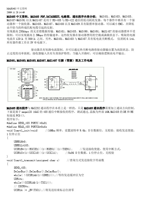
MAX481,MAX483,MAX485,MAX487,MAX1487引脚(管脚)图及工作电路MAX485通讯程序与MAX232通讯程序在本质上是一样的,只是MAX485通讯程序需要加上通讯方向控制。
下面是基于mega128 16AU的485通信中断接收的程序,调试通过,晶振为外部16M,MAX485的DE和RE短接连PC0口,程序如下:#define SEND_485 PORTC|=0x01#define READ_485 PORTC&=0xfevoid Usart1_init(void) //16Mhz频率,设置波特率9.6k,8位数据位,无校验,接收发送使能,1位停止位{UBRR1H=0;UBRR1L=103;UCSR1B=(1<<RXCIE1)|(1<<RXEN1)|(1<<TXEN1); //发送接收使能,使用中断方式,UCSR1C=(1<<UCSZ10)|(1<<UCSZ11); //0x06 8位数据,1位停止位,无校验}void Usart1_transmit(unsigned char c) //查询方式发送接收字符函数{SEND_485;DelayBus();DelayBus();DelayBus();while( !(UCSR1A&(1<<UDRE1)));//等待发送缓冲区为空UDR1=c;while(!(UCSR1A&(1<<TXC1)));// UDCR0=c;UCSR1A |= _BV(TXC1);//将发送结束标志位清零// SET_BIT(UCSR1A,);READ_485;direction++;}SIGNAL(SIG_UART1_RECV)//serial port 1 {if(UCSR1A&(1<<RXC1)){rec1buff=UDR1;rec1_flag=1;。
MAXIM 化数字电位器MAX5481, MAX5482, MAX5483, MAX548 说明书

ENGLISH•简体中文•日本語•概述状况状况:生产中。
下载Notes MAX5481Linear13-WireSerial SPINon-Volatile102410253519.6$1.95@1kMAX548250$1.95 @1kMAX548310$1.95 @1kMAX548450$1.95 @1k查看所有Digital Potentiometers (128)引脚配置相关产品MAX5494,MAX5495,MAX5496, ...10位、双路、非易失、线性变化数字电位器类似产品:浏览其它类似产品线查看所有Digital Potentiometers (128产品)顶标MAX5481顶标MAX5482顶标MAX5483顶标MAX5484新品发布[ 2005-08-03 ]应用工程师帮助选型,下个工作日回复参数搜索应用帮助概述技术文档定购信息概述关键特性应用/使用关键指标图表注释、注解相关产品数据资料应用笔记评估板设计指南可靠性报告软件/模型价格与供货样品在线订购封装信息无铅信息参考文献: 19-3708 Rev. 4; 2008-03-12本页最后一次更新: 2008-03-27联络我们:信息反馈、提出问题 • 对该网页的评价 • 发送本网页 • 隐私权政策 • 法律声明 © 2010 Maxim Integrated Products版权所有General DescriptionThe MAX5481–MAX5484 10-bit (1024-tap) nonvolatile,linear-taper, programmable voltage-dividers and vari-able resistors perform the function of a mechanical potentiometer, but replace the mechanics with a pin-configurable 3-wire serial SPI™-compatible interface or up/down digital interface. The MAX5481/MAX5482 are 3-terminal voltage-dividers and the MAX5483/MAX5484are 2-terminal variable resistors.The MAX5481–MAX5484 feature an internal, non-volatile, electrically erasable programmable read-only memory (EEPROM) that stores the wiper position for ini-tialization during power-up. The 3-wire SPI-compatible serial interface allows communication at data rates up to 7MHz. A pin-selectable up/down digital interface is also available.The MAX5481–MAX5484 are ideal for applications requiring digitally controlled potentiometers. Two end-to-end resistance values are available (10k Ωand 50k Ω) in a voltage-divider or a variable-resistor configuration (see the Selector G uide ). The nominal resistor temperature coefficient is 35ppm/°C end-to-end, and only 5ppm/°C ratiometric, making these devices ideal for applications requiring low-temperature-coefficient voltage-dividers,such as low-drift, programmable gain-amplifiers.The MAX5481–MAX5484 operate with either a +2.7V to +5.25V single power supply or ±2.5V dual power sup-plies. These devices consume 400µA (max) of supply current when writing data to the nonvolatile memory and 1.0µA (max) of standby supply current. The MAX5481–MAX5484 are available in a space-saving (3mm x 3mm), 16-pin TQFN, or a 14-pin TSSOP pack-age and are specified over the extended (-40°C to +85°C) temperature range.ApplicationsFeatures♦1024 Tap Positions♦Power-On Recall of Wiper Position from Nonvolatile Memory♦16-Pin (3mm x 3mm x 0.8mm) TQFN or 14-Pin TSSOP Package♦35ppm/°C End-to-End Resistance Temperature Coefficient♦5ppm/°C Ratiometric Temperature Coefficient ♦10kΩand 50kΩEnd-to-End Resistor Values♦Pin-Selectable SPI-Compatible Serial Interface or Up/Down Digital Interface ♦1µA (max) Standby Current♦Single +2.7V to +5.25V Supply Operation ♦Dual ±2.5V Supply OperationMAX5481–MAX548410-Bit, Nonvolatile, Linear-Taper DigitalPotentiometers________________________________________________________________Maxim Integrated Products1Ordering InformationPin Configurations19-3708; Rev 5; 4/10For pricing delivery, and ordering information please contact Maxim Direct at 1-888-629-4642,or visit Maxim’s website at .Selector Guide appears at end of data sheet.SPI is a trademark of Motorola, Inc.temperature range.+Denotes a lead(Pb)-free/RoHS-compliant package.*EP = Exposed pad.Ordering Information continued at end of data sheet.Gain and Offset AdjustmentLCD Contrast Adjustment Pressure SensorsLow-Drift Programmable Gain AmplifiersMechanical Potentiometer ReplacementM A X 5481–M A X 548410-Bit, Nonvolatile, Linear-Taper Digital PotentiometersABSOLUTE MAXIMUM RATINGSStresses beyond those listed under “Absolute Maximum Ratings” may cause permanent damage to the device. These are stress ratings only, and functional operation of the device at these or any other conditions beyond those indicated in the operational sections of the specifications is not implied. Exposure to absolute maximum rating conditions for extended periods may affect device reliability.V DD to GND...........................................................-0.3V to +6.0V V SS to GND............................................................-3.5V to +0.3V V DD to V SS .............................................................-0.3V to +6.0V H, L, W to V SS ..................................(V SS - 0.3V) to (V DD + 0.3V)CS , SCLK(INC ), DIN(U/D ), SPI/UD to GND..-0.3V to (V DD + 0.3V)Maximum Continuous Current into H, L, and WMAX5481/MAX5483.........................................................±5mA MAX5482/MAX5484......................................................±1.0mA Maximum Current into Any Other Pin...............................±50mAContinuous Power Dissipation (T A = +70°C)16-Pin TQFN (derate 17.5mW/°C above +70°C).....1398.6mW 14-Pin TSSOP (derate 9.1mW/°C above +70°C)..........727mW Operating Temperature Range ...........................-40°C to +85°C Junction Temperature......................................................+150°C Storage Temperature Range.............................-60°C to +150°C Lead Temperature (soldering, 10s).................................+300°C Soldering Temperature (reflow).......................................+260°CELECTRICAL CHARACTERISTICSMAX5481–MAX548410-Bit, Nonvolatile, Linear-Taper DigitalPotentiometers_______________________________________________________________________________________3ELECTRICAL CHARACTERISTICS (continued)(V DD = +2.7V to +5.25V, V SS = V GND = 0V, V H = V DD , V L = 0V, T A = -40°C to +85°C, unless otherwise noted. Typical values are at V DD = +5.0V, T A = +25°C, unless otherwise noted.) (Note 1)M A X 5481–M A X 548410-Bit, Nonvolatile, Linear-Taper Digital Potentiometers 4_______________________________________________________________________________________TIMING CHARACTERISTICSNote 2:The DNL and INL are measured with the device configured as a voltage-divider with H = V DD and L = V SS . The wiper termi-nal (W) is unloaded and measured with a high-input-impedance voltmeter.Note 3:The DNL_R and INL_R are measured with D.N.C. unconnected and L = V SS = 0V. For V DD = +5V, the wiper terminal is dri-ven with a source current of I W = 80µA for the 50k Ωdevice and 400µA for the 10k Ωdevice. For V DD = +3V, the wiper termi-nal is driven with a source current of 40µA for the 50k Ωdevice and 200µA for the 10k Ωdevice.Note 4:The wiper resistance is measured using the source currents given in Note 3.Note 5:The device draws higher supply current when the digital inputs are driven with voltages between (V DD - 0.5V) and (V GND +0.5V). See Supply Current vs. Digital Input Voltage in the Typical Operating Characteristics .Note 6:Wiper settling test condition uses the voltage-divider configuration with a 10pF load on W. Transition code from 00000 00000to 01111 01111 and measure the time from CS going high to the wiper voltage settling to within 0.5% of its final value.MAX5481–MAX548410-Bit, Nonvolatile, Linear-Taper DigitalPotentiometers_______________________________________________________________________________________5-1.0-0.6-0.8-0.2-0.40.200.40.80.61.002563841285126407688961024DNL vs. CODE (MAX5483)CODED N L (L S B )V DD = 2.7V-1.0-0.6-0.8-0.2-0.40.200.40.80.61.002563841285126407688961024DNL vs. CODE (MAX5483)CODED N L (L S B )V DD = 5V-2.0-1.0-1.50-0.50.51.01.5 2.0INL vs. CODE (MAX5483)I N L (L S B )V DD = 2.7V02563841285126407688961024CODE-2.0-1.0-1.50-0.50.51.01.5 2.0INL vs. CODE (MAX5483)I N L (L S B )V DD = 3V2563841285126407688961024CODE-2.0-1.0-1.50-0.50.51.01.5 2.0INL vs. CODE (MAX5483)I N L (L S B )V DD = 5V02563841285126407688961024CODE-1.0-0.6-0.8-0.2-0.40.200.40.80.61.002563841285126407688961024DNL vs. CODE (MAX5481)CODED N L (L S B )-1.0-0.6-0.8-0.2-0.40.200.40.80.61.002563841285126407688961024DNL vs. CODE (MAX5481)CODED N L (L S B )V DD = 5V-1.0-0.6-0.8-0.2-0.40.200.40.80.61.002563841285126407688961024INL vs. CODE (MAX5481)CODEI N L (L S B )-1.0-0.6-0.8-0.2-0.40.200.40.80.61.002563841285126407688961024INL vs. CODE (MAX5481)CODEI N L (L S B )Typical Operating Characteristics(V DD = 5.0V, V SS = 0V, T A = +25°C, unless otherwise noted.)M A X 5481–M A X 548410-Bit, Nonvolatile, Linear-Taper Digital Potentiometers 6_______________________________________________________________________________________-1.0-0.6-0.8-0.2-0.40.200.40.80.61.002563841285126407688961024DNL vs. CODE (MAX5484)CODED N L (L S B )-1.0-0.6-0.8-0.2-0.40.200.40.80.61.002563841285126407688961024DNL vs. CODE (MAX5484)CODED N L (L S B )-1.0-0.6-0.8-0.2-0.40.200.40.80.61.002563841285126407688961024INL vs. CODE (MAX5484)CODEI N L (L S B )-1.0-0.6-0.8-0.2-0.40.200.40.80.61.002563841285126407688961024INL vs. CODE (MAX5484)CODEI N L (L S B )-1.0-0.6-0.8-0.2-0.40.200.40.80.61.002563841285126407688961024DNL vs. CODE (MAX5482)CODED N L (L S B )-1.0-0.6-0.8-0.2-0.40.200.40.80.61.002563841285126407688961024DNL vs. CODE (MAX5482)CODED N L (L S B )-1.0-0.6-0.8-0.2-0.40.200.40.80.61.002563841285126407688961024INL vs. CODE (MAX5482)CODEI N L (L S B )V DD = 2.7V-1.0-0.6-0.8-0.2-0.40.200.40.80.61.02563841285126407688961024INL vs. CODE (MAX5482)CODEI N L (L S B )V DD = 5V02010403050607080WIPER RESISTANCE vs. CODE (VARIABLE RESISTOR, T A = -40°C)M A X 5481 t o c 18R W (Ω)2563841285126407688961024CODETypical Operating Characteristics (continued)(V DD = 5.0V, V SS = 0V, T A = +25°C, unless otherwise noted.)MAX5481–MAX5484Typical Operating Characteristics (continued)(V DD = 5.0V, V SS = 0V, T A = +25°C, unless otherwise noted.)10-Bit, Nonvolatile, Linear-Taper DigitalPotentiometers_______________________________________________________________________________________702010403050607080WIPER RESISTANCE vs. CODE (VARIABLE RESISTOR, T A = +25°C)M A X 5481 t oc 19R W (Ω)2563841285126407688961024CODE2010403050607080WIPER RESISTANCE vs. CODE (VARIABLE RESISTOR, T A = +85°C)M A X 5481 t o c 20R W (Ω)2563841285126407688961024CODE10302050604070W-TO-L RESISTANCE vs. CODE(MAX5484)R W L (k Ω)02563841285126407688961024CODE02641012814W-TO-L RESISTANCE vs. CODE(MAX5483)R W L (k Ω)2563841285126407688961024CODE18.018.519.019.520.020.521.021.522.0012345WIPER RESISTANCE vs. WIPER VOLTAGE(VARIABLE RESISTOR)WIPER VOLTAGE (V)R W (Ω)-2.0-1.5-1.0-0.500.51.01.52.0-40-1510356085END-TO-END (R HL ) % CHANGE vs. TEMPERATURE (VOLTAGE-DIVIDER)M A X 5481 t o c 24TEMPERATURE (°C)E N D -T O -E N D R E S I S T A N C E C H A N G E (%)-2.0-1.5-1.0-0.500.51.01.52.0-40-1510356085WIPER-TO-END RESISTANCE (R WL ) % CHANGE vs. TEMPERATURE (VARIABLE RESISTOR)TEMPERATURE (°C)W I P E R -T O -E N D R E S I S T A N C E C H A N G E (%)00.30.90.61.21.5-4010-15356085STANDBY SUPPLY CURRENTvs. TEMPERATURETEMPERATURE (°C)I D D (μA )DIGITAL SUPPLY CURRENT vs. DIGITAL INPUT VOLTAGEDIGITAL INPUT VOLTAGE (V)I D D (μA )4.54.03.53.02.52.01.51.00.5110100100010,0000.15.0M A X 5481–M A X 548410-Bit, Nonvolatile, Linear-Taper Digital Potentiometers Typical Operating Characteristics (continued)(Circuit of Figure 1, T A = +25°C, unless otherwise noted.)1μs/divTAP-TO-TAP SWITCHING TRANSIENTRESPONSE (MAX5481)V W(AC-COUPLED)20mV/divCS 2V/divH = V DD , L = GND C W = 10pFFROM CODE 01 1111 1111TO CODE 10 0000 00004μs/divTAP-TO-TAP SWITCHING TRANSIENTRESPONSE (MAX5482)V W(AC-COUPLED)20mV/divCS 2V/divH = V DD , L = GND C W = 10pFFROM CODE 01 1111 1111TO CODE 10 0000 0000WIPER RESPONSE vs. FREQUENCY(MAX5481)FREQUENCY (kHz)G A I N (d B )100101-20-15-10-5-250.11000WIPER RESPONSE vs. FREQUENCY(MAX5482)FREQUENCY (kHz)G A I N (d B )100101-20-15-10-50-250.11000THD+N vs. FREQUENCY(MAX5481)FREQUENCY (kHz)T H D +N (%)1010.10.0010.010.11100.00010.01100THD+N vs. FREQUENCY(MAX5482)FREQUENCY (kHz)T H D +N (%)1010.10.0010.010.11100.00010.0110004020806012010014018016020002563841285126407688961024RATIOMETRIC TEMPERATURE COEFFICIENT vs. CODECODER A T I O M E T R I C T E M P C O (p p m )100300200500600400700VARIABLE-RESISTOR TEMPERATURECOEFFICIENT vs. CODET C V R (p p m )02563841285126407688961024CODE10-Bit, Nonvolatile, Linear-Taper DigitalPotentiometersPin DescriptionMAX5481–MAX5484M A X 5481–M A X 548410-Bit, Nonvolatile, Linear-Taper Digital Potentiometers Pin Description (continued)(MAX5483/MAX5484 Variable Resistors)MAX5481–MAX548410-Bit, Nonvolatile, Linear-Taper DigitalPotentiometersFunctional DiagramsM A X 5481–M A X 548410-Bit, Nonvolatile, Linear-Taper Digital Potentiometers Detailed DescriptionThe MAX5481/MAX5482 linear programmable voltage-dividers and the MAX5483/MAX5484 variable resistors feature 1024 tap points (10-bit resolution) (see the Functional Diagrams ). These devices consist of multi-ple strings of equal resistor segments with a wiper con-tact that moves among the 1024 points through a pin-selectable 3-wire SPI-compatible serial interface or up/down interface. The MAX5481/MAX5483 provide a total end-to-end resistance of 10k Ω, and the MAX5482/MAX5484 have an end-to-end resistance of 50k Ω. The MAX5481/MAX5482 allow access to the high, low, and wiper terminals for a standard voltage-divider configuration.MAX5481/MAX5482 ProgrammableVoltage-DividersThe MAX5481/MAX5482 programmable voltage-dividers provide a weighted average of the voltage between the H and L inputs at the W output. Both devices feature 10-bit resolution and provide up to 1024 tap points between the H and L voltages. Ideally,the V L voltage occurs at the wiper terminal (W) when all data bits are zero and the V H voltage occurs at the wiper terminal when all data bits are one. The step size (1 LSB) voltage is equal to the voltage applied across terminals H and L divided by 210. Calculate the wiper voltage V Was follows:Functional Diagrams (continued)MAX5481–MAX548410-Bit, Nonvolatile, Linear-Taper DigitalPotentiometerswhere D is the decimal equivalent of the 10 data bits writ-ten (0 to 1023), V HL is the voltage difference between the H and L terminals:The MAX5481 includes a total end-to-end resistance value of 10k Ωwhile the MAX5482 features an end-to-end resistance value of 50k Ω. These devices are not intended to be used as a variable resistor . Wiper cur-rent creates a nonlinear voltage drop in series with the wiper. To ensure temperature drift remains within speci-fications, do not pull current through the voltage-divider wiper. Connect the wiper to a high-impedance node.Figures 1 and 2 show the behavior of the MAX5481’s resistance from W to H and from W to L. This does not apply to the variable-resistor devicesMAX5483/MAX5484 Variable ResistorsThe MAX5483/MAX5484 provide a programmable resistance between W and L. The MAX5483 features a total end-to-end resistance value of 10k Ω, while the MAX5484 provides an end-to-end resistance value of 50k Ω. The programmable resolution of this resistance is equal to the nominal end-to-end resistance divided by 1024 (10-bit resolution). For example, each nominal segment resistance is 9.8Ωand 48.8Ωfor the MAX5483and the MAX5484, respectively.wiper position from the 1024 possible positions, result-ing in 1024 values for the resistance from W to L.Calculate the resistance from W to L (R WL ) by using the where D is decimal equivalent of the 10 data bits writ-ten, R W-L is the nominal end-to-end resistance, and R Z is the zero-scale error. Table 1 shows the values of R WL at selected codes for the MAX5483/MAX5484.Digital InterfaceConfigure the MAX5481–MAX5484 by a pin-selectable,3-wire, SPI-compatible serial data interface or an up/down interface. Drive SPI/UD high to select the 3-wire SPI-compatible interface. Pull SPI/UD low to select the up/down interface.V FSE V andV ZSE V FSE HL ZSE HL =⎡⎣⎢⎤⎦⎥=⎡⎣⎢⎤⎦⎥10241024,Figure 1. Resistance from W to H vs. Code (10k ΩVoltage-Divider)Figure 2. Resistance from W to L vs. Code (10k ΩVoltage-Divider)M A X 5481–M A X 548410-Bit, Nonvolatile, Linear-Taper Digital Potentiometers SPI-Compatible Serial InterfaceDrive SPI/UD high to enable the 3-wire SPI-compatible serial interface (see Figure 3). This write-only interface contains three inputs: chip select (CS ), data in (DIN(U/D )), and data clock (SCLK(INC )). Drive CS low to load the data at DIN(U/D ) synchronously into the shift register on each SCLK(INC ) rising edge.The WRITE command (C1, C0 = 00) requires 24 clock cycles to transfer the command and data (Figure 4a).The COPY commands (C1, C0 = 10 or 11) use either eight clock cycles to transfer the command bits (Figure 4b) or 24 clock cycles with the last 16 data bits disre-garded by the device.After loading the data into the shift register, drive CS high to latch the data into the appropriate control regis-ter. Keep CS low during the entire serial data stream to avoid corruption of the data. Table 2 shows the com-mand decoding.Write Wiper RegisterData written to this register (C1, C0 = 00) controls the wiper position. The 10 data bits (D9–D0) indicate the position of the wiper. For example, if DIN(U/D ) = 00 00000000, the wiper moves to the position closest to L. If DIN(U/D ) = 11 1111 1111, the wiper moves closest to H.This command writes data to the volatile random access memory (RAM), leaving the NV register unchanged. When the device powers up, the data stored in the NV register transfers to the wiper register,moving the wiper to the stored position. Figure 5 shows how to write data to the wiper register.Table 2. Command Decoding*X = Don’t care.Figure 3. SPI-Compatible Serial-Interface Timing Diagram (SPI/UD = 1)10-Bit, Nonvolatile, Linear-Taper DigitalPotentiometers ArrayMAX5481–MAX5484Figure4. Serial SPI-Compatible Interface FormatFigure5. Write Wiper Register OperationM A X 5481–M A X 548410-Bit, Nonvolatile, Linear-Taper Digital Potentiometers Copy Wiper Register to NV RegisterThe copy wiper register to NV register command (C1,C0 = 10) stores the current position of the wiper to the NV register for use at power-up. Figure 6 shows how to copy data from wiper register to NV register. The oper-ation takes up to 12ms (max) after CS goes high to complete and no other operation should be performed until completion.Copy NV Register to Wiper RegisterThe copy NV register to wiper register (C1, C0 = 11)restores the wiper position to the current value stored in the NV register. Figure 7 shows how to copy data from the NV register to the wiper register.Digital Up/Down InterfaceFigure 8 illustrates an up/down serial-interface timing diagram. In digital up/down interface mode (SPI/UD =0), the logic inputs CS , DIN(U/D ), and SCLK(INC ) con-trol the wiper position and store it in nonvolatile memory (see Table 3). The chip-select (CS ) input enables the serial interface when low and disables the interface when high. The position of the wiper is stored in the nonvolatile register when CS transitions from low to high while SCLK(INC ) is high.When the serial interface is active (CS low), a high-to-low (falling edge) transition on SCLK(INC ) increments or decrements the internal 10-bit counter depending on the state of DIN(U/D ). If DIN(U/D ) is high, the wiper increments. If DIN(U/D ) is low, the wiper decrements.The device stores the value of the wiper position in the nonvolatile memory when CS transitions from low to high while SCLK(INC ) is high. The host system can disablethe serial interface and deselect the device without stor-ing the latest wiper position in the nonvolatile memory by keeping SCLK(INC ) low while taking CS high.Upon power-up, the MAX5481–MAX5484 load the value of nonvolatile memory into the wiper register, and set the wiper position to the value last stored.Figure 6. Copy Wiper Register to NV Register OperationFigure 7. Copy NV Register to Wiper Register OperationMAX5481–MAX548410-Bit, Nonvolatile, Linear-Taper DigitalPotentiometersStandby ModeThe MAX5481–MAX5484 feature a low-power standby mode. When the device is not being programmed, it enters into standby mode and supply current drops to 0.5µA (typ).Nonvolatile MemoryThe internal EEPROM consists of a nonvolatile register that retains the last value stored prior to power-down.The nonvolatile register is programmed to midscale at the factory. The nonvolatile memory is guaranteed for 50 years of wiper data retention and up to 200,000wiper write cycles.Power-UpUpon power-up, the MAX5481–MAX5484 load the data stored in the nonvolatile wiper register into the volatile wiper register, updating the wiper position with the data stored in the nonvolatile wiper register.Applications InformationThe MAX5481–MAX5484 are ideal for circuits requiring digitally controlled adjustable resistance, such as LCD contrast control (where voltage biasing adjusts the dis-play contrast), or programmable filters with adjustable gain and/or cutoff frequency.Positive LCD Bias ControlFigures 9 and 10 show an application where a voltage-divider or a variable resistor is used to make an adjustable, positive LCD-bias voltage. The op amp pro-vides buffering and gain to the voltage-divider network made by the programmable voltage-divider (Figure 9) or to a fixed resistor and a variable resistor (see Figure 10).Programmable Gain and Offset AdjustmentFigure 11 shows an application where a voltage-divider and a variable resistor are used to make a programma-ble gain and offset adjustment.Figure 8. Up/Down Serial-Interface Timing Diagram (SPI/UD = 0)M A X 5481–M A X 548410-Bit, Nonvolatile, Linear-Taper Digital Potentiometers 18______________________________________________________________________________________Programmable FilterFigure 12 shows the configuration for a 1st-order pro-grammable filter using two variable resistors. Adjust R2for the gain and adjust R3 for the cutoff frequency. Use the following equations to estimate the gain (G) and the 3dB cutoff frequency (f C):Figure 10. Positive LCD Bias Control Using a Variable ResistorFigure 12. Programmable FilterFigure 11. Programmable Gain/Offset AdjustmentFigure 9. Positive LCD Bias Control Using a Voltage-DividerMAX5481–MAX548410-Bit, Nonvolatile, Linear-Taper DigitalPotentiometers______________________________________________________________________________________19Chip InformationPROCESS: BiCMOSSelector GuidePin Configurations (continued)Ordering Information (continued)Note: All devices are specified over the -40°C to +85°C operating temperature range.+Denotes a lead(Pb)-free/RoHS-compliant package.*EP = Exposed pad.Package InformationFor the latest package outline information and land patterns, go to /packages . Note that a “+”, “#”, or “-” in the package code indicates RoHS status only. Package draw-ings may show a different suffix character, but the drawing per-tains to the package regardless of RoHS status.M A X 5481–M A X 548410-Bit, Nonvolatile, Linear-Taper Digital Potentiometers Maxim cannot assume responsibility for use of any circuitry other than circuitry entirely embodied in a Maxim product. No circuit patent licenses are implied. Maxim reserves the right to change the circuitry and specifications without notice at any time.20____________________Maxim Integrated Products, 120 San Gabriel Drive, Sunnyvale, CA 94086 408-737-7600©2010 Maxim Integrated ProductsMaxim is a registered trademark of Maxim Integrated Products, Inc.。
max542中文翻译

MAX541/MAX542串行输入,电压输出,16位的数字 - 模拟转换器(DAC)的操作从单一的+5 V电源。
他们提供的16位performance随温度(±1LSB INL和DNL)无任何调整。
DAC输出缓冲,结果ING在一个低电源的0.3毫安电流和低失调错误的1LSB。
DAC输出范围为0V至VREF。
对于双极歌剧TION,匹配缩放电阻器中提供了MAX542为使用外部精密运算放大器(如MAX400),产生一个± VREF输出摆动。
MAX542还包括开尔文检测CON -nections为参考和模拟接地引脚降低布局敏感度。
一个16位串行字是用来加载数据到DAC闩锁。
10MHz时,3线串行接口兼容与SPI™/ QSPI™/ MICROWIRE™,它也接口直接与光耦合器需要的应用程序隔离TION。
上电复位电路清除DAC输出0V (单极模式)电源时,最初应用。
MAX541是8引脚塑料DIP和SO包。
MAX542是14引脚塑料DIP和SO封装。
特点全部16位性能,无需调整+5 V的单电源供电低功耗:1.5MW1碌小号建立时间非缓冲电压输出直接驱动60K鈩负载SPI / QSPI / Microwire兼容串行接口上电复位电路清除DAC输出0V(单极模式)施密特触发器输入直接光电耦合器接口引脚:1-RFB-反馈电阻。
连接到外部运算放大器的双极模式的输出。
2-OUT-DAC输出电压3-AGNDF-模拟地(力)4- AGNDS -模拟地(感)5-REFS-参考电压输入(感)。
REFS 连接到外部+2.5 V基准。
6- REFF-参考电压输入(强制)。
REFF 连接到外部+2.5 V基准。
7- CS-片选输入8- SCLK-串行时钟输入。
占空比必须在40%和60%。
9-NC-无连接。
在内部没有连接。
10- DIN-串行数据输入11-LDAC-LDAC输入。
下降沿更新内部DAC锁存器。
OPA541AM中文资料

®
OPA541
High Power Monolithic OPERATIONAL AMPLIFIER
FEATURES
q POWER SUPPLIES TO ±40V q OUTPUT CURRENT TO 10A PEAK q PROGRAMMABLE CURRENT LIMIT q INDUSTRY-STANDARD PIN OUT q FET INPUT q TO-3 AND LOW-COST POWER PLASTIC
Common-mode ............................................................. ±VS Temperature: Pin solder, 10s ........................................................ +300°C
Pinout is compatible with popular hybrid power amplifiers such as the OPA511, OPA512 and the 3573.
APPLICATIONS
q MOTOR DRIVER q SERVO AMPLIFIER q SYNCHRO EXCITATION q AUDIO AMPLIFIER q PROGRAMMABLE POWER SUPPLY
®
OPA541
2
元器件交易网
CONNECTION DIAGRAMS
Top View
+VS 3
+In 4
–In 5 6
–VS
NC 2
1
Current Sense
RCL
max485esa中文资料
General DescriptionThe MAX481, MAX483, MAX485, MAX487–MAX491, andMAX1487 are low-power transceivers for RS-485 and RS-422 communication. Each part contains one driver and onereceiver. The MAX483, MAX487, MAX488, and MAX489feature reduced slew-rate drivers that minimize E MI andreduce reflections caused by improperly terminated cables,thus allowing error-free data transmission up to 250kbps.The driver slew rates of the MAX481, MAX485, MAX490,MAX491, and MAX1487 are not limited, allowing them totransmit up to 2.5Mbps.These transceivers draw between 120µA and 500µA ofsupply current when unloaded or fully loaded with disableddrivers. Additionally, the MAX481, MAX483, and MAX487have a low-current shutdown mode in which they consumeonly 0.1µA. All parts operate from a single 5V supply.Drivers are short-circuit current limited and are protectedagainst excessive power dissipation by thermal shutdowncircuitry that places the driver outputs into a high-imped-ance state. The receiver input has a fail-safe feature thatguarantees a logic-high output if the input is open circuit.The MAX487 and MAX1487 feature quarter-unit-loadreceiver input impedance, allowing up to 128 MAX487/MAX1487 transceivers on the bus. Full-duplex communi-cations are obtained using the MAX488–MAX491, whilethe MAX481, MAX483, MAX485, MAX487, and MAX1487are designed for half-duplex applications.________________________Applications Low-Power RS-485 Transceivers Low-Power RS-422 Transceivers Level Translators Transceivers for EMI-Sensitive Applications Industrial-Control Local Area Networks__Next Generation Device Features o For Fault-Tolerant Applications MAX3430: ±80V Fault-Protected, Fail-Safe, 1/4Unit Load, +3.3V, RS-485 Transceiver MAX3440E–MAX3444E: ±15kV ESD-Protected,±60V Fault-Protected, 10Mbps, Fail-Safe, RS-485/J1708 Transceivers o For Space-Constrained Applications MAX3460–MAX3464: +5V, Fail-Safe, 20Mbps,Profibus RS-485/RS-422 Transceivers MAX3362: +3.3V, High-Speed, RS-485/RS-422Transceiver in a SOT23 Package MAX3280E–MAX3284E: ±15kV ESD-Protected,52Mbps, +3V to +5.5V, SOT23, RS-485/RS-422,True Fail-Safe Receivers MAX3293/MAX3294/MAX3295: 20Mbps, +3.3V,SOT23, RS-485/RS-422 Transmitters o For Multiple Transceiver Applications MAX3030E–MAX3033E: ±15kV ESD-Protected,+3.3V, Quad RS-422 Transmitters o For Fail-Safe Applications MAX3080–MAX3089: Fail-Safe, High-Speed (10Mbps), Slew-Rate-Limited RS-485/RS-422Transceiverso For Low-Voltage ApplicationsMAX3483E/MAX3485E/MAX3486E/MAX3488E/MAX3490E/MAX3491E: +3.3V Powered, ±15kVESD-Protected, 12Mbps, Slew-Rate-Limited,True RS-485/RS-422 Transceivers For pricing, delivery, and ordering information, please contact Maxim Direct at1-888-629-4642, or visit Maxim Integrated’s website at .______________________________________________________________Selection Table19-0122; Rev 10; 9/14PARTNUMBERHALF/FULL DUPLEX DATA RATE (Mbps) SLEW-RATE LIMITED LOW-POWER SHUTDOWN RECEIVER/DRIVER ENABLE QUIESCENT CURRENT (μA) NUMBER OF RECEIVERS ON BUS PIN COUNT MAX481Half 2.5No Yes Yes 300328MAX483Half 0.25Yes Yes Yes 120328MAX485Half 2.5No No Yes 300328MAX487Half 0.25Yes Yes Yes 1201288MAX488Full 0.25Yes No No 120328MAX489Full 0.25Yes No Yes 1203214MAX490Full 2.5No No No 300328MAX491Full 2.5No No Yes 3003214MAX1487 Half 2.5No No Yes 2301288Ordering Information appears at end of data sheet.找电子元器件上宇航军工MAX481/MAX483/MAX485/MAX487–MAX491/MAX1487Low-Power, Slew-Rate-LimitedRS-485/RS-422 TransceiversPackage Information For the latest package outline information and land patterns, go to . Note that a “+”, “#”, or “-”in the package code indicates RoHS status only. Package drawings may show a different suffix character, but the drawing pertains to the package regardless of RoHS status.16Low-Power, Slew-Rate-Limited RS-485/RS-422 TransceiversMAX481/MAX483/MAX485/MAX487–MAX491/MAX1487Maxim Integrated cannot assume responsibility for use of any circuitry other than circuitry entirely embodied in a Maxim Integrated product. No circuit patent licenses are implied. Maxim Integrated reserves the right to change the circuitry and specifications without notice at any time. The parametric values (min and max limits) shown in the Electrical Characteristics table are guaranteed. Other parametric values quoted in this data sheet are provided for guidance.Maxim Integrated 160 Rio Robles, San Jose, CA 95134 USA 1-408-601-100017©2014 Maxim Integrated Products, Inc.Maxim Integrated and the Maxim Integrated logo are trademarks of Maxim Integrated Products, Inc.。
MAX412CSA+中文资料

Features
o Voltage Noise: 2.4nV/√Hz (max) at 1kHz o 2.5mA Supply Current Per Amplifier o Low Supply Voltage Operation: ±2.4V to ±5V o 28MHz Unity-Gain Bandwidth o 4.5V/µs Slew Rate o 250µV (max) Offset Voltage (MAX410/MAX412) o 115dB (min) Voltage Gain o Available in an Ultra-Small TDFN Package
________________________________________________________________ Maxim Integrated Products 1
For pricing, delivery, and ordering information, please contact Maxim/Dallas Direct! at 1-888-629-4642, or visit Maxim’s website at .
MAX410B, MAX412B, MAX414B
1000Hz (Note 2)
Input Noise-Current Density
in
fO = 10Hz fO = 1000Hz
Common-Mode Input Voltage
VCM
Common-Mode Rejection Ratio Power-Supply Rejection Ratio
Stresses beyond those listed under “Absolute Maximum Ratings” may cause permanent damage to the device. These are stress ratings only, and functional operation of the device at these or any other conditions beyond those indicated in the operational sections of the specifications is not implied. Exposure to absolute maximum rating conditions for extended periods may affect device reliability.
MAX485CSA中文资料
For pricing, delivery, and ordering information,please contact Maxim/Dallas Direct!at 1-888-629-4642, or visit Maxim’s website at .General DescriptionThe MAX481, MAX483, MAX485, MAX487–MAX491, and MAX1487 are low-power transceivers for RS-485 and RS-422 communication. Each part contains one driver and one receiver. The MAX483, MAX487, MAX488, and MAX489feature reduced slew-rate drivers that minimize EMI and reduce reflections caused by improperly terminated cables,thus allowing error-free data transmission up to 250kbps.The driver slew rates of the MAX481, MAX485, MAX490,MAX491, and MAX1487 are not limited, allowing them to transmit up to 2.5Mbps.These transceivers draw between 120µA and 500µA of supply current when unloaded or fully loaded with disabled drivers. Additionally, the MAX481, MAX483, and MAX487have a low-current shutdown mode in which they consume only 0.1µA. All parts operate from a single 5V supply.Drivers are short-circuit current limited and are protected against excessive power dissipation by thermal shutdown circuitry that places the driver outputs into a high-imped-ance state. The receiver input has a fail-safe feature that guarantees a logic-high output if the input is open circuit.The MAX487 and MAX1487 feature quarter-unit-load receiver input impedance, allowing up to 128 MAX487/MAX1487 transceivers on the bus. Full-duplex communi-cations are obtained using the MAX488–MAX491, while the MAX481, MAX483, MAX485, MAX487, and MAX1487are designed for half-duplex applications.________________________ApplicationsLow-Power RS-485 Transceivers Low-Power RS-422 Transceivers Level TranslatorsTransceivers for EMI-Sensitive Applications Industrial-Control Local Area Networks__Next Generation Device Features♦For Fault-Tolerant ApplicationsMAX3430: ±80V Fault-Protected, Fail-Safe, 1/4Unit Load, +3.3V, RS-485 TransceiverMAX3440E–MAX3444E: ±15kV ESD-Protected,±60V Fault-Protected, 10Mbps, Fail-Safe, RS-485/J1708 Transceivers♦For Space-Constrained ApplicationsMAX3460–MAX3464: +5V, Fail-Safe, 20Mbps,Profibus RS-485/RS-422 TransceiversMAX3362: +3.3V, High-Speed, RS-485/RS-422Transceiver in a SOT23 PackageMAX3280E–MAX3284E: ±15kV ESD-Protected,52Mbps, +3V to +5.5V, SOT23, RS-485/RS-422,True Fail-Safe ReceiversMAX3293/MAX3294/MAX3295: 20Mbps, +3.3V,SOT23, RS-855/RS-422 Transmitters ♦For Multiple Transceiver ApplicationsMAX3030E–MAX3033E: ±15kV ESD-Protected,+3.3V, Quad RS-422 Transmitters ♦For Fail-Safe ApplicationsMAX3080–MAX3089: Fail-Safe, High-Speed (10Mbps), Slew-Rate-Limited RS-485/RS-422Transceivers♦For Low-Voltage ApplicationsMAX3483E/MAX3485E/MAX3486E/MAX3488E/MAX3490E/MAX3491E: +3.3V Powered, ±15kV ESD-Protected, 12Mbps, Slew-Rate-Limited,True RS-485/RS-422 TransceiversMAX481/MAX483/MAX485/MAX487–MAX491/MAX1487Low-Power, Slew-Rate-Limited RS-485/RS-422 Transceivers______________________________________________________________Selection Table19-0122; Rev 8; 10/03Ordering Information appears at end of data sheet.M A X 481/M A X 483/M A X 485/M A X 487–M A X 491/M A X 1487Low-Power, Slew-Rate-Limited RS-485/RS-422 Transceivers 2_______________________________________________________________________________________ABSOLUTE MAXIMUM RATINGSSupply Voltage (V CC ).............................................................12V Control Input Voltage (RE , DE)...................-0.5V to (V CC + 0.5V)Driver Input Voltage (DI).............................-0.5V to (V CC + 0.5V)Driver Output Voltage (A, B)...................................-8V to +12.5V Receiver Input Voltage (A, B).................................-8V to +12.5V Receiver Output Voltage (RO).....................-0.5V to (V CC +0.5V)Continuous Power Dissipation (T A = +70°C)8-Pin Plastic DIP (derate 9.09mW/°C above +70°C)....727mW 14-Pin Plastic DIP (derate 10.00mW/°C above +70°C)..800mW 8-Pin SO (derate 5.88mW/°C above +70°C).................471mW14-Pin SO (derate 8.33mW/°C above +70°C)...............667mW 8-Pin µMAX (derate 4.1mW/°C above +70°C)..............830mW 8-Pin CERDIP (derate 8.00mW/°C above +70°C).........640mW 14-Pin CERDIP (derate 9.09mW/°C above +70°C).......727mW Operating Temperature RangesMAX4_ _C_ _/MAX1487C_ A...............................0°C to +70°C MAX4__E_ _/MAX1487E_ A.............................-40°C to +85°C MAX4__MJ_/MAX1487MJA...........................-55°C to +125°C Storage Temperature Range.............................-65°C to +160°C Lead Temperature (soldering, 10sec).............................+300°CDC ELECTRICAL CHARACTERISTICS(V CC = 5V ±5%, T A = T MIN to T MAX , unless otherwise noted.) (Notes 1, 2)Stresses beyond those listed under “Absolute Maximum Ratings” may cause permanent damage to the device. These are stress ratings only, and functional operation of the device at these or any other conditions beyond those indicated in the operational sections of the specifications is not implied. Exposure to absolute maximum rating conditions for extended periods may affect device reliability.V V IN = -7VV IN = 12V V IN = -7V V IN = 12V Input Current (A, B)I IN2V TH k Ω48-7V ≤V CM ≤12V, MAX487/MAX1487R INReceiver Input Resistance -7V ≤V CM ≤12V, all devices except MAX487/MAX1487R = 27Ω(RS-485), Figure 40.4V ≤V O ≤2.4VR = 50Ω(RS-422)I O = 4mA, V ID = -200mV I O = -4mA, V ID = 200mV V CM = 0V-7V ≤V CM ≤12V DE, DI, RE DE, DI, RE MAX487/MAX1487,DE = 0V, V CC = 0V or 5.25VDE, DI, RE R = 27Ωor 50Ω, Figure 4R = 27Ωor 50Ω, Figure 4R = 27Ωor 50Ω, Figure 4DE = 0V;V CC = 0V or 5.25V,all devices except MAX487/MAX1487CONDITIONSk Ω12µA ±1I OZRThree-State (high impedance)Output Current at ReceiverV 0.4V OL Receiver Output Low Voltage 3.5V OH Receiver Output High Voltage mV 70∆V TH Receiver Input Hysteresis V -0.20.2Receiver Differential Threshold Voltage-0.2mA 0.25mA-0.81.01.55V OD2Differential Driver Output (with load)V 2V 5V OD1Differential Driver Output (no load)µA±2I IN1Input CurrentV 0.8V IL Input Low Voltage V 2.0V IH Input High Voltage V 0.2∆V OD Change in Magnitude of Driver Common-Mode Output Voltage for Complementary Output States V 0.2∆V OD Change in Magnitude of Driver Differential Output Voltage for Complementary Output States V 3V OC Driver Common-Mode Output VoltageUNITS MINTYPMAX SYMBOL PARAMETERMAX481/MAX483/MAX485/MAX487–MAX491/MAX1487Low-Power, Slew-Rate-Limited RS-485/RS-422 Transceivers_______________________________________________________________________________________3SWITCHING CHARACTERISTICS—MAX481/MAX485, MAX490/MAX491, MAX1487(V CC = 5V ±5%, T A = T MIN to T MAX , unless otherwise noted.) (Notes 1, 2)DC ELECTRICAL CHARACTERISTICS (continued)(V CC = 5V ±5%, T A = T MIN to T MAX , unless otherwise noted.) (Notes 1, 2)ns 103060t PHLDriver Rise or Fall Time Figures 6 and 8, R DIFF = 54Ω, C L1= C L2= 100pF ns MAX490M, MAX491M MAX490C/E, MAX491C/E2090150MAX481, MAX485, MAX1487MAX490M, MAX491MMAX490C/E, MAX491C/E MAX481, MAX485, MAX1487Figures 6 and 8, R DIFF = 54Ω,C L1= C L2= 100pF MAX481 (Note 5)Figures 5 and 11, C RL = 15pF, S2 closedFigures 5 and 11, C RL = 15pF, S1 closed Figures 5 and 11, C RL = 15pF, S2 closed Figures 5 and 11, C RL = 15pF, S1 closed Figures 6 and 10, R DIFF = 54Ω,C L1= C L2= 100pFFigures 6 and 8,R DIFF = 54Ω,C L1= C L2= 100pF Figures 6 and 10,R DIFF = 54Ω,C L1= C L2= 100pF CONDITIONS ns 510t SKEW ns50200600t SHDNTime to ShutdownMbps 2.5f MAX Maximum Data Rate ns 2050t HZ Receiver Disable Time from High ns 103060t PLH 2050t LZ Receiver Disable Time from Low ns 2050t ZH Driver Input to Output Receiver Enable to Output High ns 2050t ZL Receiver Enable to Output Low 2090200ns ns 134070t HZ t SKD Driver Disable Time from High |t PLH - t PHL |DifferentialReceiver Skewns 4070t LZ Driver Disable Time from Low ns 4070t ZL Driver Enable to Output Low 31540ns51525ns 31540t R , t F 2090200Driver Output Skew to Output t PLH , t PHL Receiver Input to Output4070t ZH Driver Enable to Output High UNITS MIN TYP MAX SYMBOL PARAMETERFigures 7 and 9, C L = 100pF, S2 closed Figures 7 and 9, C L = 100pF, S1 closed Figures 7 and 9, C L = 15pF, S1 closed Figures 7 and 9, C L = 15pF, S2 closedM A X 481/M A X 483/M A X 485/M A X 487–M A X 491/M A X 1487Low-Power, Slew-Rate-Limited RS-485/RS-422 Transceivers 4_______________________________________________________________________________________SWITCHING CHARACTERISTICS—MAX483, MAX487/MAX488/MAX489(V CC = 5V ±5%, T A = T MIN to T MAX , unless otherwise noted.) (Notes 1, 2)SWITCHING CHARACTERISTICS—MAX481/MAX485, MAX490/MAX491, MAX1487 (continued)(V CC = 5V ±5%, T A = T MIN to T MAX , unless otherwise noted.) (Notes 1, 2)3001000Figures 7 and 9, C L = 100pF, S2 closed Figures 7 and 9, C L = 100pF, S1 closed Figures 5 and 11, C L = 15pF, S2 closed,A - B = 2VCONDITIONSns 40100t ZH(SHDN)Driver Enable from Shutdown toOutput High (MAX481)nsFigures 5 and 11, C L = 15pF, S1 closed,B - A = 2Vt ZL(SHDN)Receiver Enable from Shutdownto Output Low (MAX481)ns 40100t ZL(SHDN)Driver Enable from Shutdown toOutput Low (MAX481)ns 3001000t ZH(SHDN)Receiver Enable from Shutdownto Output High (MAX481)UNITS MINTYP MAX SYMBOLPARAMETERt PLH t SKEW Figures 6 and 8, R DIFF = 54Ω,C L1= C L2= 100pFt PHL Figures 6 and 8, R DIFF = 54Ω,C L1= C L2= 100pFDriver Input to Output Driver Output Skew to Output ns 100800ns ns 2000MAX483/MAX487, Figures 7 and 9,C L = 100pF, S2 closedt ZH(SHDN)Driver Enable from Shutdown to Output High2502000ns2500MAX483/MAX487, Figures 5 and 11,C L = 15pF, S1 closedt ZL(SHDN)Receiver Enable from Shutdown to Output Lowns 2500MAX483/MAX487, Figures 5 and 11,C L = 15pF, S2 closedt ZH(SHDN)Receiver Enable from Shutdown to Output Highns 2000MAX483/MAX487, Figures 7 and 9,C L = 100pF, S1 closedt ZL(SHDN)Driver Enable from Shutdown to Output Lowns 50200600MAX483/MAX487 (Note 5) t SHDN Time to Shutdownt PHL t PLH , t PHL < 50% of data period Figures 5 and 11, C RL = 15pF, S2 closed Figures 5 and 11, C RL = 15pF, S1 closed Figures 5 and 11, C RL = 15pF, S2 closed Figures 5 and 11, C RL = 15pF, S1 closed Figures 7 and 9, C L = 15pF, S2 closed Figures 6 and 10, R DIFF = 54Ω,C L1= C L2= 100pFFigures 7 and 9, C L = 15pF, S1 closed Figures 7 and 9, C L = 100pF, S1 closed Figures 7 and 9, C L = 100pF, S2 closed CONDITIONSkbps 250f MAX 2508002000Maximum Data Rate ns 2050t HZ Receiver Disable Time from High ns 25080020002050t LZ Receiver Disable Time from Low ns 2050t ZH Receiver Enable to Output High ns 2050t ZL Receiver Enable to Output Low ns ns 1003003000t HZ t SKD Driver Disable Time from High I t PLH - t PHL I DifferentialReceiver SkewFigures 6 and 10, R DIFF = 54Ω,C L1= C L2= 100pFns 3003000t LZ Driver Disable Time from Low ns 2502000t ZL Driver Enable to Output Low ns Figures 6 and 8, R DIFF = 54Ω,C L1= C L2= 100pFns 2502000t R , t F 2502000Driver Rise or Fall Time ns t PLH Receiver Input to Output2502000t ZH Driver Enable to Output High UNITS MIN TYP MAX SYMBOL PARAMETERMAX481/MAX483/MAX485/MAX487–MAX491/MAX1487Low-Power, Slew-Rate-Limited RS-485/RS-422 Transceivers_______________________________________________________________________________________530002.5OUTPUT CURRENT vs.RECEIVER OUTPUT LOW VOLTAGE525M A X 481-01OUTPUT LOW VOLTAGE (V)O U T P U T C U R R E N T (m A )1.515100.51.02.0203540450.90.1-50-252575RECEIVER OUTPUT LOW VOLTAGE vs.TEMPERATURE0.30.7TEMPERATURE (°C)O U T P U TL O W V O L T A G E (V )500.50.80.20.60.40100125-20-41.5 2.0 3.0 5.0OUTPUT CURRENT vs.RECEIVER OUTPUT HIGH VOLTAGE-8-16M A X 481-02OUTPUT HIGH VOLTAGE (V)O U T P U T C U R R E N T (m A )2.5 4.0-12-18-6-14-10-203.54.5 4.83.2-50-252575RECEIVER OUTPUT HIGH VOLTAGE vs.TEMPERATURE3.64.4TEMPERATURE (°C)O U T P UT H I G H V O L T A G E (V )0504.04.63.44.23.83.01001259000 1.0 3.0 4.5DRIVER OUTPUT CURRENT vs.DIFFERENTIAL OUTPUT VOLTAGE1070M A X 481-05DIFFERENTIAL OUTPUT VOLTAGE (V)O U T P U T C U R R E N T (m A )2.0 4.05030806040200.5 1.5 2.53.5 2.31.5-50-2525125DRIVER DIFFERENTIAL OUTPUT VOLTAGEvs. TEMPERATURE1.72.1TEMPERATURE (°C)D I F FE R E N T I A L O U T P U T V O L T A G E (V )751.92.21.62.01.8100502.4__________________________________________Typical Operating Characteristics(V CC = 5V, T A = +25°C, unless otherwise noted.)NOTES FOR ELECTRICAL/SWITCHING CHARACTERISTICSNote 1:All currents into device pins are positive; all currents out of device pins are negative. All voltages are referenced to deviceground unless otherwise specified.Note 2:All typical specifications are given for V CC = 5V and T A = +25°C.Note 3:Supply current specification is valid for loaded transmitters when DE = 0V.Note 4:Applies to peak current. See Typical Operating Characteristics.Note 5:The MAX481/MAX483/MAX487 are put into shutdown by bringing RE high and DE low. If the inputs are in this state for lessthan 50ns, the parts are guaranteed not to enter shutdown. If the inputs are in this state for at least 600ns, the parts are guaranteed to have entered shutdown. See Low-Power Shutdown Mode section.M A X 481/M A X 483/M A X 485/M A X 487–M A X 491/M A X 1487Low-Power, Slew-Rate-Limited RS-485/RS-422 Transceivers 6___________________________________________________________________________________________________________________Typical Operating Characteristics (continued)(V CC = 5V, T A = +25°C, unless otherwise noted.)120008OUTPUT CURRENT vs.DRIVER OUTPUT LOW VOLTAGE20100M A X 481-07OUTPUT LOW VOLTAGE (V)O U T P U T C U R R E N T (m A )6604024801012140-1200-7-5-15OUTPUT CURRENT vs.DRIVER OUTPUT HIGH VOLTAGE-20-80M A X 481-08OUTPUT HIGH VOLTAGE (V)O U T P U T C U R R E N T (m A )-31-603-6-4-2024-100-40100-40-60-2040100120MAX1487SUPPLY CURRENT vs. TEMPERATURE300TEMPERATURE (°C)S U P P L Y C U R R E N T (µA )20608050020060040000140100-50-2550100MAX481/MAX485/MAX490/MAX491SUPPLY CURRENT vs. TEMPERATURE300TEMPERATURE (°C)S U P P L Y C U R R E N T (µA )257550020060040000125100-50-2550100MAX483/MAX487–MAX489SUPPLY CURRENT vs. TEMPERATURE300TEMPERATURE (°C)S U P P L Y C U R R E N T (µA )257550020060040000125MAX481/MAX483/MAX485/MAX487–MAX491/MAX1487Low-Power, Slew-Rate-Limited RS-485/RS-422 Transceivers_______________________________________________________________________________________7______________________________________________________________Pin DescriptionFigure 1. MAX481/MAX483/MAX485/MAX487/MAX1487 Pin Configuration and Typical Operating CircuitM A X 481/M A X 483/M A X 485/M A X 487–M A X 491/M A X 1487__________Applications InformationThe MAX481/MAX483/MAX485/MAX487–MAX491 and MAX1487 are low-power transceivers for RS-485 and RS-422 communications. The MAX481, MAX485, MAX490,MAX491, and MAX1487 can transmit and receive at data rates up to 2.5Mbps, while the MAX483, MAX487,MAX488, and MAX489 are specified for data rates up to 250kbps. The MAX488–MAX491 are full-duplex trans-ceivers while the MAX481, MAX483, MAX485, MAX487,and MAX1487 are half-duplex. In addition, Driver Enable (DE) and Receiver Enable (RE) pins are included on the MAX481, MAX483, MAX485, MAX487, MAX489,MAX491, and MAX1487. When disabled, the driver and receiver outputs are high impedance.MAX487/MAX1487:128 Transceivers on the BusThe 48k Ω, 1/4-unit-load receiver input impedance of the MAX487 and MAX1487 allows up to 128 transceivers on a bus, compared to the 1-unit load (12k Ωinput impedance) of standard RS-485 drivers (32 trans-ceivers maximum). Any combination of MAX487/MAX1487 and other RS-485 transceivers with a total of 32 unit loads or less can be put on the bus. The MAX481/MAX483/MAX485 and MAX488–MAX491 have standard 12k ΩReceiver Input impedance.Low-Power, Slew-Rate-Limited RS-485/RS-422 Transceivers 8_______________________________________________________________________________________Figure 2. MAX488/MAX490 Pin Configuration and Typical Operating CircuitFigure 3. MAX489/MAX491 Pin Configuration and Typical Operating CircuitMAX483/MAX487/MAX488/MAX489:Reduced EMI and ReflectionsThe MAX483 and MAX487–MAX489 are slew-rate limit-ed, minimizing EMI and reducing reflections caused by improperly terminated cables. Figure 12 shows the dri-ver output waveform and its Fourier analysis of a 150kHz signal transmitted by a MAX481, MAX485,MAX490, MAX491, or MAX1487. High-frequency har-monics with large amplitudes are evident. Figure 13shows the same information displayed for a MAX483,MAX487, MAX488, or MAX489 transmitting under the same conditions. Figure 13’s high-frequency harmonics have much lower amplitudes, and the potential for EMI is significantly reduced.MAX481/MAX483/MAX485/MAX487–MAX491/MAX1487Low-Power, Slew-Rate-Limited RS-485/RS-422 Transceivers_______________________________________________________________________________________9_________________________________________________________________Test CircuitsFigure 4. Driver DC Test Load Figure 5. Receiver Timing Test LoadFigure 6. Driver/Receiver Timing Test Circuit Figure 7. Driver Timing Test LoadM A X 481/M A X 483/M A X 485/M A X 487–M A X 491/M A X 1487Low-Power, Slew-Rate-Limited RS-485/RS-422 Transceivers 10_______________________________________________________Switching Waveforms_________________Function Tables (MAX481/MAX483/MAX485/MAX487/MAX1487)Figure 8. Driver Propagation DelaysFigure 9. Driver Enable and Disable Times (except MAX488 and MAX490)Figure 10. Receiver Propagation DelaysFigure 11. Receiver Enable and Disable Times (except MAX488and MAX490)Table 1. TransmittingTable 2. ReceivingLow-Power Shutdown Mode (MAX481/MAX483/MAX487)A low-power shutdown mode is initiated by bringing both RE high and DE low. The devices will not shut down unless both the driver and receiver are disabled.In shutdown, the devices typically draw only 0.1µA of supply current.RE and DE may be driven simultaneously; the parts are guaranteed not to enter shutdown if RE is high and DE is low for less than 50ns. If the inputs are in this state for at least 600ns, the parts are guaranteed to enter shutdown.For the MAX481, MAX483, and MAX487, the t ZH and t ZL enable times assume the part was not in the low-power shutdown state (the MAX485/MAX488–MAX491and MAX1487 can not be shut down). The t ZH(SHDN)and t ZL(SHDN)enable times assume the parts were shut down (see Electrical Characteristics ).It takes the drivers and receivers longer to become enabled from the low-power shutdown state (t ZH(SHDN ), t ZL(SHDN)) than from the operating mode (t ZH , t ZL ). (The parts are in operating mode if the –R —E –,DE inputs equal a logical 0,1 or 1,1 or 0, 0.)Driver Output ProtectionExcessive output current and power dissipation caused by faults or by bus contention are prevented by two mechanisms. A foldback current limit on the output stage provides immediate protection against short cir-cuits over the whole common-mode voltage range (see Typical Operating Characteristics ). In addition, a ther-mal shutdown circuit forces the driver outputs into a high-impedance state if the die temperature rises excessively.Propagation DelayMany digital encoding schemes depend on the differ-ence between the driver and receiver propagation delay times. Typical propagation delays are shown in Figures 15–18 using Figure 14’s test circuit.The difference in receiver delay times, | t PLH - t PHL |, is typically under 13ns for the MAX481, MAX485,MAX490, MAX491, and MAX1487 and is typically less than 100ns for the MAX483 and MAX487–MAX489.The driver skew times are typically 5ns (10ns max) for the MAX481, MAX485, MAX490, MAX491, and MAX1487, and are typically 100ns (800ns max) for the MAX483 and MAX487–MAX489.MAX481/MAX483/MAX485/MAX487–MAX491/MAX1487Low-Power, Slew-Rate-Limited RS-485/RS-422 Transceivers______________________________________________________________________________________1110dB/div0Hz5MHz500kHz/div10dB/div0Hz5MHz500kHz/divFigure 12. Driver Output Waveform and FFT Plot of MAX481/MAX485/MAX490/MAX491/MAX1487 Transmitting a 150kHz SignalFigure 13. Driver Output Waveform and FFT Plot of MAX483/MAX487–MAX489 Transmitting a 150kHz SignalM A X 481/M A X 483/M A X 485/M A X 487–M A X 491/M A X 1487Low-Power, Slew-Rate-Limited RS-485/RS-422 Transceivers 12______________________________________________________________________________________V CC = 5V T A = +25°CV CC = 5V T A = +25°CV CC = 5V T A = +25°CV CC = 5V T A = +25°CFigure 14. Receiver Propagation Delay Test CircuitFigure 15. MAX481/MAX485/MAX490/MAX491/MAX1487Receiver t PHLFigure 16. MAX481/MAX485/MAX490/MAX491/MAX1487Receiver t PLHPHL Figure 18. MAX483, MAX487–MAX489 Receiver t PLHLine Length vs. Data RateThe RS-485/RS-422 standard covers line lengths up to 4000 feet. For line lengths greater than 4000 feet, see Figure 23.Figures 19 and 20 show the system differential voltage for the parts driving 4000 feet of 26AWG twisted-pair wire at 110kHz into 120Ωloads.Typical ApplicationsThe MAX481, MAX483, MAX485, MAX487–MAX491, and MAX1487 transceivers are designed for bidirectional data communications on multipoint bus transmission lines.Figures 21 and 22 show typical network applications circuits. These parts can also be used as line repeaters, with cable lengths longer than 4000 feet, as shown in Figure 23.To minimize reflections, the line should be terminated at both ends in its characteristic impedance, and stub lengths off the main line should be kept as short as possi-ble. The slew-rate-limited MAX483 and MAX487–MAX489are more tolerant of imperfect termination.MAX481/MAX483/MAX485/MAX487–MAX491/MAX1487Low-Power, Slew-Rate-Limited RS-485/RS-422 Transceivers______________________________________________________________________________________13DIV Y -V ZRO5V 0V1V0V -1V5V 0V2µs/divFigure 19. MAX481/MAX485/MAX490/MAX491/MAX1487 System Differential Voltage at 110kHz Driving 4000ft of Cable Figure 20. MAX483, MAX487–MAX489 System Differential Voltage at 110kHz Driving 4000ft of CableFigure 21. MAX481/MAX483/MAX485/MAX487/MAX1487 Typical Half-Duplex RS-485 NetworkM A X 481/M A X 483/M A X 485/M A X 487–M A X 491/M A X 1487Low-Power, Slew-Rate-Limited RS-485/RS-422 Transceivers 14______________________________________________________________________________________Figure 22. MAX488–MAX491 Full-Duplex RS-485 NetworkFigure 23. Line Repeater for MAX488–MAX491Isolated RS-485For isolated RS-485 applications, see the MAX253 and MAX1480 data sheets.MAX481/MAX483/MAX485/MAX487–MAX491/MAX1487Low-Power, Slew-Rate-Limited RS-485/RS-422 Transceivers______________________________________________________________________________________15_______________Ordering Information_________________Chip TopographiesMAX481/MAX483/MAX485/MAX487/MAX1487N.C. RO 0.054"(1.372mm)0.080"(2.032mm)DE DIGND B N.C.V CCARE * Contact factory for dice specifications.__Ordering Information (continued)M A X 481/M A X 483/M A X 485/M A X 487–M A X 491/M A X 1487Low-Power, Slew-Rate-Limited RS-485/RS-422 Transceivers 16______________________________________________________________________________________TRANSISTOR COUNT: 248SUBSTRATE CONNECTED TO GNDMAX488/MAX490B RO 0.054"(1.372mm)0.080"(2.032mm)N.C. DIGND Z A V CCYN.C._____________________________________________Chip Topographies (continued)MAX489/MAX491B RO 0.054"(1.372mm)0.080"(2.032mm)DE DIGND Z A V CCYREMAX481/MAX483/MAX485/MAX487–MAX491/MAX1487Low-Power, Slew-Rate-Limited RS-485/RS-422 Transceivers______________________________________________________________________________________17Package Information(The package drawing(s) in this data sheet may not reflect the most current specifications. For the latest package outline information go to /packages .)S O I C N .E P SM A X 481/M A X 483/M A X 485/M A X 487–M A X 491/M A X 1487Low-Power, Slew-Rate-Limited RS-485/RS-422 Transceivers 18______________________________________________________________________________________Package Information (continued)(The package drawing(s) in this data sheet may not reflect the most current specifications. For the latest package outline information go to /packages .)MAX481/MAX483/MAX485/MAX487–MAX491Low-Power, Slew-Rate-Limited RS-485/RS-422 TransceiversMaxim cannot assume responsibility for use of any circuitry other than circuitry entirely embodied in a Maxim product. No circuit patent licenses are implied. Maxim reserves the right to change the circuitry and specifications without notice at any time.Maxim Integrated Products, 120 San Gabriel Drive, Sunnyvale, CA 94086 408-737-7600 ____________________19©2003 Maxim Integrated ProductsPrinted USAis a registered trademark of Maxim Integrated Products.M A X 481/M A X 483/M A X 485/M A X 487–M A X 491/M A X 1487P D I P N .E PSPackage Information (continued)(The package drawing(s) in this data sheet may not reflect the most current specifications. For the latest package outline information go to /packages .)。
MAX541

MAX541是美国MAXIM公司生产的D/A转换芯片,它是低功耗(1.5mW),无缓冲电压输出,能够驱动60kv的负载,用单+5V电源工作的串行16位数模转换器。
其转换时间为1μs,输出电压变换范围为0V~VREF[16]。
下图为芯片的管脚图,并将MAX541的管脚功能列于表3-3中。
表3-3 MAX541管脚功能表
引脚号引脚名称引脚功能
1 OUT DAC 电压输出
2 AGND 模拟地
3 REF 电压参考输入,链接到外接的+2.5V参
考
4 CS 芯片选择,低电平有效
5 SCLK 串行时钟输入
6 DIN 串行数据输入
7 DGND 数字地
8 VDD +5V电源电压
MAX的工作原理是:模拟输出电压VOUT的输出范围由输入不同的数字代码来有规律的控制,当输入的16位数字代码全为0时,输出电压VOUT为0。
当输入的16位数字代码全为1时,输出电压约为VREF即2.5V。
于是VOUT的变化规律是,16位数字代码从0开始,每次加1,一直到全为1,对应的输出电压一直从0开始每次增加VREF*(1/65536)。
1111 1111 1111 1111 VREF*(65535/65536)
…….
…….
1000 0000 0000 0000 VREF*(32768/65536)
…….
……
0000 0000 0000 0001 VREF*(1/65536)
0000 0000 0000 0000 VREF *( 0/65536)。
OPA541中文资料
2®OPA541SPECIFICATIONSELECTRICALAt T C = +25°C and V S = ±35VDC, unless otherwise noted.OPA541AM/APOPA541BM/SM PARAMETERCONDITIONSMINTYP MAX MINTYP MAX UNITS INPUT OFFSET VOLTAGE V OS±2±10±0.1±1mV vs Temperature Specified Temperature Range±20±40±15±30µV/°C vs Supply Voltage V S = ±10V to ±V MAX±2.5±10T T µV/V vs Power±20±60T T µV/W INPUT BIAS CURRENT I B450T T pA INPUT OFFSET CURRENT I OS±1±30T TpA Specified Temperature Range5T nA INPUT CHARACTERISTICS Common-Mode Voltage Range Specified Temperature Range±(|V S | – 6)±(|V S | – 3)T T V Common-Mode Rejection V CM = (|±V S | – 6V)95113TT dB Input Capacitance 5T pF Input Impedance, DC 1T T ΩGAIN CHARACTERISTICS Open Loop Gain at 10Hz R L = 6Ω9097TT dB Gain-Bandwidth Product 1.6T MHz OUTPUTVoltage SwingI O = 5A, Continuous±(|V S | – 5.5)±(|V S | – 4.5)T T V I O = 2A ±(|V S | – 4.5)±(|V S | – 3.6)T T V I O = 0.5A±(|V S | – 4)±(|V S | – 3.2)T T V Current, Peak 910T T A AC PERFORMANCE Slew Rate610T T V/µs Power Bandwidth R L = 8Ω, V O = 20Vrms4555TT kHz Settling Time to 0.1%2V Step2Tµs Capacitive Load Specified Temperature Range, G = 1 3.3T nF Specified Temperature Range, G >10SOA (1)T Phase MarginSpecified Temperature Range, R L = 8Ω40T Degrees POWER SUPPLYPower Supply Voltage, ±V S Specified Temperature Range±10±30±35T±35±40V Current, Quiescent 2025TTmA THERMAL RESISTANCE θJC (Junction-to-Case)(2)AC Output f > 60Hz2.5°C/W θJC (2)DC Output 3°C/W θJA (Junction-to-Ambient)No Heat Sink40°C/W OPA541AP (Plastic)40°C/W TEMPERATURE RANGE T CASEAM, BM, AP–25+85T T °C SM–55+125°CT Specification same as OPA541AM/AP.NOTE: (1) SOA is the Safe Operating Area shown in Figure 1. (2) Plastic package may require insulator which typically adds 1°C/W.The information provided herein is believed to be reliable; however, BURR-BROWN assumes no responsibility for inaccuracies or omissions. BURR-BROWN assumes no responsibility for the use of this information, and all use of such information shall be entirely at the user’s own risk. Prices and specifications are subject to change without notice. No patent rights or licenses to any of the circuits described herein are implied or granted to any third party. BURR-BROWN does not authorize or warrant any BURR-BROWN product for use in life support devices and/or systems.3®OPA541CONNECTION DIAGRAMSORDERING INFORMATIONTEMPERATURECONTINUOUS PRODUCT PACKAGE RANGE CURRENT OPA541AP Power Plastic–25°C to +85°C 5A at 25°C OPA541AM TO-3–25°C to +85°C 5A at 25°C OPA541BM TO-3–25°C to +85°C 5A at 25°C OPA541SMTO-3–55°C to +125°C5A at 25°CABSOLUTE MAXIMUM RATINGSSupply Voltage, +V S to –V S ...............................................................80V Output Current.............................................................................see SOA Power Dissipation, Internal (1)...........................................................125W Input Voltage: Differential ....................................................................±V SCommon-mode.............................................................±V STemperature: Pin solder, 10s........................................................+300°CJunction (1)...............................................................+150°CTemperature Range:AM, BM SMStorage ....................................................................–65°C to +150°C Operating (case)......................................................–55°C to +125°C APStorage ......................................................................–40°C to +85°C Operating (case)........................................................–25°C to +85°C NOTE: (1) Long term operation at the maximum junction temperature will result in reduced product life. Derate internal power dissipation to achieve high MTTF.PACKAGE INFORMATIONPACKAGE DRAWINGPRODUCT PACKAGE NUMBER (1)OPA541AP Power Plastic242OPA541AM TO-3030OPA541BM TO-3030OPA541SMTO-3030NOTE: (1) For detailed drawing and dimension table, please see end of data sheet, or Appendix C of Burr-Brown IC Data Book.This integrated circuit can be damaged by ESD. Burr-Brown recommends that all integrated circuits be handled with appropriate precautions. Failure to observe proper handling and installation procedures can cause damage.ESD damage can range from subtle performance degradation to complete device failure. Precision integrated circuits may be more susceptible to damage because very small parametric changes could cause the device not to meet its published specifications.4®OPA5411010.10.010.001101001k 10k100kFrequency (Hz)T H D + N o i s e (%)TOTAL HARMONIC DISTORTION + NOISEvs FREQUENCY1k10010V o l t a g e N o i s e D e n s i t y (n V /√Hz )VOLTAGE NOISE DENSITYvs FREQUENCY1101001k10k100kFrequency (Hz)6543210012345678910I (A)OUT|±V | – |V | (V )OU T S OUTPUT VOLTAGE SWING vs OUTPUT CURRENT1.31.21.110.90.80.70.62030405060708090+V + |–V | (V)S SN o r m a l i z ed I NORMALIZED QUIESCENT CURRENT vs TOTAL POWER SUPPLY VOLTAGEQ1109070503010–101101001k 10k 100k 1M 10MFrequency (Hz)V o l t a g e G a i n (d B )OPEN-LOOP GAIN AND PHASEvs FREQUENCY–45–90–135–180P h a s e (D e g r e e s )–2502550751001251001010.10.010.001I n p u t B i as C u r r e n t (n A )Temperature (°C)INPUT BIAS CURRENT vs TEMPERATURETYPICAL PERFORMANCE CURVESAt T A = +25°C, V S = ±35VDC, unless otherwise noted.5®OPA5411201101009080706050101001k10k100k1MFrequency (Hz)C M R R (d B )COMMON-MODE REJECTIONvs FREQUENCY1010.10.010.1110R ( )ΩCL I (A )L I M I TCURRENT LIMIT vs RESISTANCE LIMITTYPICAL PERFORMANCE CURVES (CONT)At T A = +25°C, V S = ±35VDC, unless otherwise noted.Time (1µs/division)DYNAMIC RESPONSEV o l t a g e (2V /d i v i s i o n)1010.10.010.1110R ( )ΩCL I (A )L I M I TCURRENT LIMIT vs RESISTANCE LIMITvs TEMPERATURE6®OPA541θHS =T CASE – T AMBIENTP D (max)INSTALLATION INSTRUCTIONSPOWER SUPPLIESThe OPA541 is specified for operation from power supplies up to ±40V. It can also be operated from unbalanced power supplies or a single power supply, as long as the total power supply voltage does not exceed 80V. The power supplies should be bypassed with low series impedance capacitors such as ceramic or tantalum. These should be located as near as practical to the amplifier’s power supply pins. Good power amplifier circuit layout is, in general, like good high frequency layout. Consider the path of large power supply and output currents. Avoid routing these connections near low-level input circuitry to avoid waveform distortion and oscillations.CURRENT LIMITInternal current limit circuitry is controlled by a single external resistor, R CL . Output load current flows through this external resistor. The current limit is activated when the voltage across this resistor is approximately a base-emitter turn-on voltage. The value of the current limit resistor is approximately:(AM, BM, SM)R CL =– 0.057(AP)R CL =– 0.020.809|I LIM |0.813|I LIM |Because of the internal structure of the OPA541, the actual current limit depends on whether current is positive or negative. The above R CL gives an average value. For a given R CL , +I OUT will actually be limited at about 10% below the expected level, while –I OUT will be limited about 10% above the expected level.The current limit value decreases with increasing tempera-ture due to the temperature coefficient of a base-emitter junction voltage. Similarly, the current limit value increases at low temperatures. Current limit versus resistor value and temperature effects are shown in the Typical Performance Curves. Approximate values for R CL at other temperatures may be calculated by adjusting R CL as follows:The adjustable current limit can be set to provide protection from short circuits. The safe short-circuit current depends on power supply voltage. See the discussion on Safe Operating Area to determine the proper current limit value.Since the full load current flows through R CL , it must be selected for sufficient power dissipation. For a 5A current limit on the TO-3 package, the formula yields an R CL of 0.105Ω (0.143Ω on the power plastic package due to differ-ent internal resistances). A continuous 5A through 0.105Ωwould require an R CL that can dissipate 2.625W.∆R CL =x (T – 25)–2mV|I LIM |Sinusoidal outputs create dissipation according to rms load current. For the same R CL , AC peaks would still be limited to 5A, but rms current would be 3.5A, and a current limiting resistor with a lower power rating could be used. Some applications (such as voice amplification) are assured of signals with much lower duty cycles, allowing a current resistor with a low power rating. Wire-wound resistors may be used for R CL . Some wire-wound resistors, however, have excessive inductance and may cause loop-stability prob-lems. Be sure to evaluate circuit performance with resistor type planned for production to assure proper circuit opera-tion.HEAT SINKINGPower amplifiers are rated by case temperature, not ambient temperature as with signal op amps. Sufficient heat sinking must be provided to keep the case temperature within rated limits for the maximum ambient temperature and power dissipation. The thermal resistance of the heat sink required may be calculated by:Commercially available heat sinks often specify their ther-mal resistance. These ratings are often suspect, however,since they depend greatly on the mounting environment and air flow conditions. Actual thermal performance should be verified by measurement of case temperature under the required load and environmental conditions.No insulating hardware is required when using the TO-3package. Since mica and other similar insulators typically add approximately 0.7°C/W thermal resistance, their elimi-nation significantly improves thermal performance. See Burr-Brown Application Bulletin AB-038 for further details on heat sinking. On the power plastic package, the metal tab is connected to –V S , and appropriate actions should be taken when mounting on a heat sink or chassis.SAFE OPERATING AREAThe safe operating area (SOA) plot provides comprehensive information on the power handling abilities of the OPA541.It shows the allowable output current as a function of the voltage across the conducting output transistor (see Figure 1). This voltage is equal to the power supply voltage minus the output voltage. For example, as the amplifier output swings near the positive power supply voltage, the voltage across the output transistor decreases and the device can safely provide large output currents demanded by the load.7®OPA541FIGURE 1. Safe Operating Area.Short circuit protection requires evaluation of SOA. Whenthe amplifier output is shorted to ground, the full power supply voltage is impressed across the conducting output transistor. The current limit must be set to a value which is safe for the power supply voltage used. For instance, with V S ±35V, a short to ground would force 35V across the conduc-ting power transistor. A current limit of 1.8A would be safe.Reactive, or EMF-generating, loads such as DC motors can present difficult SOA requirements. With a purely reactive load, output voltage and load current are 90° out of phase.Thus, peak output current occurs when the output voltage is zero and the voltage across the conducting transistor is equal to the full power supply voltage. See Burr-Brown Applica-tion Bulletin AB-039 for further information on evaluating SOA.REPLACING HYBRID POWER AMPLIFIERSThe OPA541 can be used in applications currently using various hybrid power amplifiers, including the OPA501,OPA511, OPA512, and 3573. Of course, the application must be evaluated to assure that the output capability and other performance attributes of the OPA541 meet the neces-sary requirement. These hybrid power amplifiers use two current limit resistors to independently set the positive and negative current limit value. Since the OPA541 uses only one current limit resistor to set both the positive and negative current limit, only one resistor (see Figure 4) need be installed. If installed, the resistor connected to pin 2 (TO-3package) is superfluous, but it does no harm.Because one resistor carries the current previously carried by two, the resistor may require a higher power rating.Minor adjustments may be required in the resistor value to achieve the same current limit value. Often, however, the change in current limit value when changing models is small compared to its variation over temperature. Many applica-tions can use the same current limit resistor.FIGURE 3. Isolating Capacitive Loads.APPLICATIONS CIRCUITSFIGURE 2. Clamping Output for EMF-Generating Loads.FIGURE 4. Replacing OPA501 with OPA541.8®OPA541FIGURE 5. Paralleled Operation, Extended SOA.FIGURE 6. Programmable Voltage Source.FIGURE 7. 16-Bit Programmable Voltage Source.。
MAX5402EUA中文资料

General Description The MAX5402 µPoT™digital potentiometer is a 256-tap variable resistor with 10kΩtotal resistance in a tiny 8-pin µMAX package. This device functions as a mechan-ical potentiometer, consisting of a fixed resistor string with a digitally controlled wiper contact. It operates from +2.7V to +5.5V single-supply voltages and uses an ultra-low 0.1µA supply current. This device also pro-vides glitchless switching between resistor taps, as well as a convenient power-on reset (POR) that sets the wiper to the midscale position at power-up. A low 5ppm/°C ratiometric temperature coefficient makes it ideal for applications requiring low drift.The MAX5402 serves well in applications requiring digi-tally controlled resistors, including adjustable voltage references and programmable gain amplifiers (PGAs).A nominal end-to-end resistor temperature coefficient of 35ppm/°C makes this part suitable for use as a variable resistor in applications such as low-tempco adjustable gain and other circuit configurations. This device is guaranteed over the extended industrial temperature range (-40°C to +85°C).________________________Applications Mechanical Potentiometer ReplacementLow-Drift PGAsAdjustable Voltage ReferencesFeatures o Small Footprint, 8-Pin µMAX Packageo Ultra-Low 100nA Supply Currento+2.7V to +5.5V Single-Supply Operationo256 Tap Positionso Low Ratiometric Temperature Coefficient5ppm/°Co Low End-to-End Resistor Temperature Coefficient35ppm/°Co Power-On Reset: Wiper Goes to Midscale(Position 128)o Glitchless Switching Between the Resistor Tapso3-Wire SPI™-Interface Compatibleo10kΩResistor ValueMAX5402 256-Tap, µPoT, Low-Drift, Digital PotentiometerPin Configuration19-1896; Rev 0; 1/01Ordering InformationµPoT is a trademark of Maxim Integrated Products.SPI is a trademark of Motorola, Inc.Maxim Integrated Products1 For price, delivery, and to place orders,please contact Maxim Distribution at 1-888-629-4642, or visit Maxim’s website at .Functional DiagramM A X 5402256-Tap, µPoT, Low-Drift,Digital PotentiometerABSOLUTE MAXIMUM RATINGSELECTRICAL CHARACTERISTICS(V DD = +5V, V H = V DD , V L = 0, T A = T MIN to T MAX . Typical values are at V DD = +5V, T A = +25°C, unless otherwise noted.)Stresses beyond those listed under “Absolute Maximum Ratings” may cause permanent damage to the device. These are stress ratings only, and functional operation of the device at these or any other conditions beyond those indicated in the operational sections of the specifications is not implied. Exposure to absolute maximum rating conditions for extended periods may affect device reliability.V DD to GND..............................................................-0.3V to +6V DIN, SCLK, CS to GND ............................................-0.3V to +6V H, L, W to GND.............................................-0.3V to (V DD + 0.3)Maximum Continuous Current into Pins H, L, and W ...........1mA Continuous Power Dissipation (T A = +70°C)8-Pin µMAX (derate 4.1mW/°C above +70°C)............330mWOperating Temperature Range ...........................-40°C to +85°C Junction Temperature......................................................+150°C Storage Temperature Range.............................-65°C to +150°C Lead Temperature (soldering, 10s).................................+300°CMAX5402256-Tap, µPoT, Low-Drift,Digital Potentiometer________________________________________________________________________________________3Note 2:The DNL and INL are measured with the potentiometer configured as a voltage-divider with H = V DD and L = 0. The wiperterminal is unloaded and measured with an ideal voltmeter.Note 3:The DNL and INL are measured with the potentiometer configured as a variable resistor. H is unconnected and L = 0. Thewiper terminal is driven with a source current of 200µA at V DD = +3V and 400µA at V DD = +5V.Note 4:The wiper resistance is the worst value measured, injecting a current, I W = V DD /R HL into terminal W.Note 5:Digital timing is guaranteed by design.ELECTRICAL CHARACTERISTICS (continued)(V DD = +5V, V H = V DD , V L = 0, T A = T MIN to T MAX . Typical values are at V DD = +5V, T A = +25°C, unless otherwise noted.)M A X 5402256-Tap, µPoT, Low-Drift,Digital Potentiometer 4_______________________________________________________________________________________Typical Operating Characteristics(T A = +25°C, unless otherwise noted.)100125150175200225250275300012345WIPER RESISTANCE vs. WIPER VOLTAGEWIPER VOLTAGE (V)W I P E R R E S I S T A N C E (Ω)-0.20-0.10-0.150.00-0.050.050.10-40-30-20-100102030405060708090END-TO-END RESISTANCE % CHANGEvs. TEMPERATUREM A X 5402 T o c 02TEMPERATURE (°C)E N D -T O -E N D R E S I S T A N C E % C H A N G E0214365798100649632128160192224256RESISTANCE vs. INPUT CODEM A X 5402 T o c 03INPUT CODE (DECIMAL)W -T O -L R E S I S T A N C E (k Ω)-0.20-0.10-0.150.050.00-0.050.200.150.100.25961283264160192224256VARIABLE RESISTOR DNLvs. INPUT CODEM A X 5402 T o c 04INPUT CODE (DECIMAL)R D N L (L S B )-0.4-0.3-0.1-0.20.10.20.00.30649632128160192224256VARIABLE RESISTOR INLvs. INPUT CODEM A X 5402 T o c 05INPUT CODE (DECIMAL)R I N L (L S B )-0.08-0.04-0.060.00-0.020.020.040.060.08649632128160192224256VOLTAGE-DIVIDER DNL vs. INPUT CODEM A X 5402 T o c 06INPUT CODE (DECIMAL)D N L (L S B )Typical Operating Characteristics (continued)(T A = +25°C, unless otherwise noted.)MAX5402256-Tap, µPoT, Low-Drift,Digital Potentiometer________________________________________________________________________________________5-0.20-0.10-0.150.00-0.050.050.100.150.20649632128160192224256VOLTAGE-DIVIDER INL vs. INPUT CODEM A X 5402 T o c 07INPUT CODE (DECIMAL)I N L (L S B )0.00.40.20.80.61.01.2-40-30-20-1001020304050607080SUPPLY CURRENT vs. TEMPERATURETEMPERATURE (°C)S U P P L Y C U R R E N T (µA )200ns/div (CODE 127 TO 128)TAP-TO-TAP SWITCHING TRANSIENT V W-L+2.49V+2.51V+5VMAX5402 toc09CS1001234510.10.010.0010.0001INPUT LOGIC VOLTAGEDIGITAL INPUT VOLTAGE (V)S U P P L Y C U R R E N T (m A )M A X 5402256-Tap, µPoT, Low-Drift,Digital Potentiometer 6_______________________________________________________________________________________Detailed DescriptionThe MAX5402 consists of 255 fixed resistors in series between pins H and L. The potentiometer wiper (pin W)can be programmed to access any one of the 256 dif-ferent tap points on the resistor string. The MAX5402has an SPI-compatible 3-wire serial data interface to control the wiper tap position. This write-only interface contains three inputs: Chip Select (CS ), Data In (DIN),and Data Clock (SCLK ). When CS is taken low, data from the DIN pin is synchronously loaded into the 8-bit serial shift register on the rising edge of each SCLK pulse (Figure 1). The MSB is shifted in first, as shown in Figure 3. Note that if CS is not kept low during the entire data stream, the data will be corrupted and the devicewill need to be reloaded. After all 8 data bits have been loaded into the shift register, they are latched into the decoder once CS is taken high. The decoder switches the potentiometer wiper to the tap position that corre-sponds to the 8-bit input data. Each resistor cell is 10k Ω/255 or 39.2Ωfor the MAX5402.The MAX5402 features POR circuitry. This sets the wiper to the midscale position at power-up by loading a binary value of 128 into the 8-bit latch. The MAX5402can be used as a variable resistor by connecting pin W to either pin H or L.Figure 1. Serial Interface Timing DiagramFigure 2. Detailed Serial Interface Timing DiagramMAX5402256-Tap, µPoT, Low-Drift,Digital Potentiometer________________________________________________________________________________________7Applications InformationThe MAX5402 is intended for a variety of circuits where accurate, fine-tuned adjustable resistance is required,such as in adjustable voltage or adjustable gain circuit configurations. The MAX5402 is used in either a poten-tiometer divider or a variable resistor configuration.Adjustable Current to Voltage ConverterFigure 4 shows the MAX5402 used with a MAX4250low-noise op amp to precisely tune a current-to-voltage converter. Pins H and W of the MAX5402 are connect-ed to the node between R3 and R2, and pin L is con-nected to ground.Adjustable Gain AmplifierThe MAX5402 is used again with the MAX4250 to make a digitally adjustable gain circuit as shown in Figure 5.The normal feedback resistor is replaced with the MAX5402 in a variable resistor configuration, so that the gain of the circuit can be digitally controlled.Adjustable Voltage ReferenceIn Figure 6, the MAX5402 is shown with the MAX6160to make an adjustable voltage reference. In this circuit,the H pin of the MAX5402 is connected to the OUT pin of the MAX6160, the L pin of the MAX5402 is connect-ed to GND, and the W pin of the MAX5402 is connect-ed to the ADJ pin of the MAX6160. The MAX5402allows precise tuning of the voltage reference output. A low 5ppm/°C ratiometric tempco allows a very stable adjustable voltage overtemperature.Figure 4. I to V ConverterFigure 5. Noninverting AmplifierFigure 3. Serial Data FormatM A X 5402256-Tap, µPoT, Low-Drift,Digital Potentiometer 8_______________________________________________________________________________________Chip InformationTRANSISTOR COUNT: 3475 PROCESS: BiCMOSFigure 6. Adjustable Voltage Reference256-Tap, µPoT, Low-Drift,Digital PotentiometerMAX5402Maxim cannot assume responsibility for use of any circuitry other than circuitry entirely embod ied in a Maxim prod uct. No circuit patent licenses are implied. Maxim reserves the right to change the circuitry and specifications without notice at any time.Maxim Integrated Products, 120 San Gabriel Drive, Sunnyvale, CA 94086 408-737-7600 _____________________9©2001 Maxim Integrated Products Printed USAis a registered trademark of Maxim Integrated Products.。
MAX5411中文资料
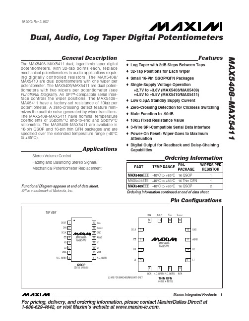
General DescriptionThe MAX5408–MAX5411 dual, logarithmic taper digital potentiometers, with 32-tap points each, replace mechanical potentiometers in audio applications requir-ing digitally controlled resistors. The MAX5408/MAX5410 are dual potentiometers with one wiper per potentiometer. The MAX5409/MAX5411 are dual poten-tiometers with two wipers per potentiometer (see Func tional Diagram ). An SPI ™-compatible serial inter-face controls the wiper positions. The MAX5408–MAX5411 have a factory-set resistance of 10k Ωper potentiometer. A zero-crossing detect feature mini-mizes the audible noise generated by wiper transitions.The MAX5408–MAX5411 have nominal temperature coefficients of 35ppm/°C end-to-end and 5ppm/°C ratiometric. The MAX5408–MAX5411 are available in 16-pin QSOP and 16-pin thin QFN packages and are specified over the extended temperature range (-40°C to +85°C).ApplicationsStereo Volume ControlFading and Balancing Stereo Signals Mechanical Potentiometer ReplacementFeatureso Log Taper with 2dB Steps Between Tapso 32-Tap Positions for Each Wiper o Small 16-Pin QSOP/QFN Packages o Single-Supply Voltage Operation+2.7V to +3.6V (MAX5408/MAX5409) +4.5V to +5.5V (MAX5410/MAX5411) o Low 0.5µA Standby Supply Currento Zero-Crossing Detection for Clickless Switching o Mute Function to -90dB o 10k ΩFixed Resistance Valueo 3-Wire SPI-Compatible Serial Data Interface o Power-On Reset: Wiper Goes to Maximum Attenuation o Digital Output for Readback and Daisy-Chaining CapabilitiesMAX5408–MAX5411Dual, Audio, Log Taper Digital Potentiometers________________________________________________________________Maxim Integrated Products 1Pin Configurations19-2049; Rev 2; 9/02For pricing, delivery, and ordering information,please contact Maxim/Dallas Direct!at 1-888-629-4642, or visit Maxim’s website at .Ordering Information continued at end of data sheet.Functional Diagram appears at end of data sheet.SPI is a trademark of Motorola, Inc.V DD , V LOGIC , CS , SCLK, DIN to GND......................-0.3V to +6V H_, L_, and W_ to GND..............................-0.3V to (V DD + 0.3V)DOUT to GND.............................................-0.3V to (V DD + 0.3V)AGND to GND.......................................................-0.3V to +0.3V Input and Output Latchup Immunity...............................±200mA Maximum Continuous Current into H_, L_, and W_.........±500µAContinuous Power Dissipation (T A = +70°C)16-Pin QSOP (derate 8.3mW/°C above +70°C)........666.7mW 16-Pin QFN (derate 18.5mW/°C above +70°C).........1481mW Operating Temperature Range ...........................-40°C to +85°C Storage Temperature Range.............................-60°C to +150°C Maximum Junction Temperature.....................................+150°C Lead Temperature (soldering, 10s).................................+300°CM A X 5408–M A X 5411Dual, Audio, Log Taper Digital PotentiometersABSOLUTE MAXIMUM RATINGSELECTRICAL CHARACTERISTICSStresses beyond those listed under “Absolute Maximum Ratings” may cause permanent damage to the device. These are stress ratings only, and functional operation of the device at these or any other conditions beyond those indicated in the operational sections of the specifications is not implied. Exposure to absolute maximum rating conditions for extended periods may affect device reliability.MAX5408–MAX5411Dual, Audio, Log Taper Digital Potentiometers_______________________________________________________________________________________3ELECTRICAL CHARACTERISTICS (continued)(V DD = +2.7V to +3.6V (MAX5408/MAX5409), V DD = +4.5V to +5.5V (MAX5410/MAX5411), V H_= V DD , V L_= 0, T A = T MIN to T MAX .Typical values are at T A = +25°C, unless otherwise specified.)Note 2:Supply current measured while changing wiper position with zero crossing enabled.Note 3:Supply current measured while wiper position is fixed.M A X 5408–M A X 5411Dual, Audio, Log Taper Digital Potentiometers 4_______________________________________________________________________________________Typical Operating Characteristics(V DD = +3V (MAX5408/MAX5409), V DD = +5V (MAX5410/MAX5411), DOUT = floating)98899098999199499599399299601.0 1.52.0 2.50.53.0 3.54.0 4.55.0WIPER RESISTANCE vs.WIPER VOLTAGEWIPER VOLTAGE (V)W I P E R R E S I S T A N C E (Ω)-0.20-0.15-0.10-0.0500.050.100.150.20-40-1510356085END-TO-END RESISTANCE % CHANGEvs. TEMPERATUREM A X 5408-11 t o c 02TEMPERATURE (°C)E N D -T O -E N D R E S I S T A N C E C H A N G E (%)-70-60-40-50-20-10-300081241620242832ATTENUATION vs. TAP POSITIONM A X 5408-11 t o c 03TAP POSITION A T T E N U A T I O N (d B )202530354045505560-40-1510356085TOTAL SUPPLY CURRENT VS. TEMPERATURETEMPERATURE (°C)T O T A L S U P P L Y C U R R E N T (µA )4µs/div TAP-TO-TAP SWITCHING TRANSIENT(ZERO-CROSSING DISABLE)V W_2V/divCS 2V/divMAX5408-11 toc05V H _ = 5V V L _ = 00.100.050.200.150.250.302.5 3.5 4.03.0 4.5 5.0 5.5LOGIC CURRENT vs. LOGIC VOLTAGELOGIC SUPPLY VOLTAGE (V)L O G I C S U P P L Y C U R R E N T (µA )MAX5408–MAX5411Dual, Audio, Log Taper Digital Potentiometers_______________________________________________________________________________________5Typical Operating Characteristics (continued)(V DD = +3V (MAX5408/MAX5409), V DD = +5V (MAX5410/MAX5411), DOUT = floating)015105202530354045502.53.53.04.04.55.05.5LOGIC CURRENT vs. LOGIC VOLTAGELOGIC SUPPLY VOLTAGE (V)L O G I C S U P P L Y C U R R E N T (µA )0.050.100.150.200.250.300.350.400.450.500.552.53.0 3.54.0 4.55.0 5.5SUPPLY CURRENT vs. SUPPLY VOLTAGEV DD (V)I D D (µA )M A X 5408–M A X 5411Dual, Audio, Log Taper Digital PotentiometersMAX5408–MAX5411Dual, Audio, Log Taper Digital PotentiometersTable 4. Mute Register Bit Definitions for MAX5409/MAX5411M A X 5408–M A X 5411DI N by 8.5 clock cycles. Force CS high to disable DOUT, placing DOUT in three-state mode. Force CS low to enable DOUT and disable three-state mode.Force CS high, after a word has been written to the MAX5408–MAX5411 to make a readback request. The next CS low period writes the requested data to DOUT.A readback request overwrites any previous data in theshift register. Note that the data appears at DOUT in the order: A0, A1, A2, D4, D3, D2, D1, D0. A0 will be available after the first high-to-low transition of SCLK when CS is low. The input continues to load the shift register while data is being read out of the MAX5408–MAX5411. The input data appears at DOUT 8.5 clock cycles later. A CS transition from low-to-high latches the input data. For any control byte, the state of SCLK must be the same for both CS low-to-high transitions and CS high-to-low transitions in order to preserve the data at DOUT while CS transitions.Zero-Crossing DetectionThe zero-crossing detection register enables the zero-crossing detect feature. The zero-crossing detect fea-ture reduces the audible noise (“clicks and pops ”) that result from wiper transitions. The wiper changes posi-tion only when the voltage at L_ is the same as the volt-age at H_. Each wiper has a zero-crossing and timeout circuit (see Figure 2). With zero-crossing enabled, the MAX5408–MAX5411 change wiper position after 50ms or when zero crossing is detected.Dual, Audio, Log Taper Digital Potentiometers 8_______________________________________________________________________________________MAX5408–MAX5411Dual, Audio, Log Taper Digital Potentiometers_______________________________________________________________________________________9Figure 4. Stereo Volume Control with Front and Rear FadeChip InformationTRANSISTOR COUNT: 12,875PROCESS: BiCMOSM A X 5408–M A X 5411Dual, Audio, Log Taper Digital Potentiometers 10______________________________________________________________________________________Figure 6. Gain ControlFigure 5. Daisy-Chaining of Serial Interfaces Ordering Information (continued)Power-On ResetThe power-on reset (POR) feature sets all the wipers to the maximum attenuation (tap position 31, -62dB) at power-up. If either V DD or V LOGIC is zero volts, a power-on reset intiates when one of the supplies is brought back to the operating voltage.Mute FunctionWhen mute is enabled, the wipers go to -90dB attenua-tion. When mute is disabled, the wiper returns to its position before mute was enabled. All wipers can be muted simultaneously or independently.Applications InformationAttenuation ControlFigure 3 shows the application of an attenuation control.The op amps are connected in a follower configuration with a fixed gain. The digitally controlled potentiometer attenuates the input signal.Stereo Volume ControlFigure 4 shows the application of stereo volume con-trol using MAX5409/MAX5411. The op amps are con-nected in a follower configuration with fixed gain. The digitally controlled potentiometer attenuates the input signals. The second wiper of each potentiometer con-trols the signal amplitude at the rear set of speakers.Daisy-ChainingFigure 5 shows an application daisy-chaining the serial-interfaces of the MAX5408–MAX5411. A single-write command updates multiple devices from a single digital port in this configuration (see Digital Serial Interface section).Gain ControlFigure 6 shows the application of a gain control. Note:Muting the potentiometer creates unpredictable behavior at the output of the op amp, and may seriously degrade the performance of the op amp.MAX5408–MAX5411Dual, Audio, Log Taper Digital Potentiometers______________________________________________________________________________________11Functional DiagramM A X 5408–M A X 5411Dual, Audio, Log Taper Digital PotentiometersPackage Information (The package drawing(s) in this data sheet may not reflect the most current specifications. For the latest package outline information,go to /packages .)MAX5408-MAX5411Dual, Audio, Log Taper Digital PotentiometersMaxim c annot assume responsibility for use of any c irc uitry other than c irc uitry entirely embodied in a Maxim produc t. No c irc uit patent lic enses are implied. Maxim reserves the right to change the circuitry and specifications without notice at any time.Maxim Integrated Products, 120 San Gabriel Drive, Sunnyvale, CA 94086 408-737-7600 ____________________13©2002 Maxim Integrated Products Printed USAis a registered trademark of Maxim Integrated Products.Package Information (continued)(The package drawing(s) in this data sheet may not reflect the most current specifications. For the latest package outline information,go to /packages .)。
CD54HC541中文资料
20 VCC 19 OE2 18 Y0 17 Y1 16 Y2 15 Y3 14 Y4 13 Y5 12 Y6 11 Y7
Functional Diagram
D0 D1 D2 D3 D4 D5 D6 D7
CD54HC541, CD54HCT541 (CERDIP)
CD74HC541 (PDIP, SOIC, TSSOP)
CD74HC541M96
-55 to 125
20 Ld SOIC
CD74HC541PW
-55 to 125
20 Ld TSSOP
CD74HC541PWR
-55 to 125
20 Ld TSSOP
CD74HCT540E
-55 to 125
20 Ld PDIP
CD74HCT540M
-55 to 125
20 Ld SOIC
TRUTH TABLE
An H X X L
OUTPUTS
540
541
L
H
Z
Z
Z
Z
H
L
3
元器件交易网 CD54/74HC540, CD74HCT540, CD54/74HC541, CD54/74HCT541
Absolute Maximum Ratings
DC Supply Voltage, VCC . . . . . . . . . . . . . . . . . . . . . . . . -0.5V to 7V DC Input Diode Current, IIK
CAUTION: These devices are sensitive to electrostatic discharge. Users should follow proper IC Handling Procedures.
MAX5484中文资料
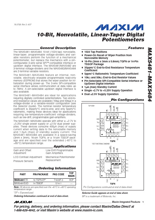
Pin Configurations continued at end of data sheet. Selector Guide appears at end of data sheet. SPI is a trademark of Motorola, Inc. 1
________________________________________________________________ Maxim Integrated Products
10-Bit, Nonvolatile, Linear-Taper Digital Potentiometers MAX5481–MAX5484
ABSOLUTE MAXIMUM RATINGS
VDD to GND ...........................................................-0.3V to +6.0V VSS to GND............................................................-3.5V to +0.3V VDD to VSS .............................................................-0.3V to +6.0V H, L, W to VSS ..................................(VSS - 0.3V) to (VDD + 0.3V) CS, SCLK(INC), DIN(U/D), SPI/UD to GND ..-0.3V to (VDD + 0.3V) Maximum Continuous Current into H, L, and W MAX5481/MAX5483.........................................................±5mA MAX5482/MAX5484......................................................±1.0mA Maximum Current into Any Other Pin ...............................±50mA Continuous Power Dissipation (TA = +70°C) 16-Pin TQFN (derate 17.5mW/°C above +70°C) .....1398.6mW 14-Pin TSSOP (derate 9.1mW/°C above +70°C) ..........727mW Operating Temperature Range ...........................-40°C to +85°C Junction Temperature ......................................................+150°C Storage Temperature Range .............................-60°C to +150°C Lead Temperature (soldering, 10s) .................................+300°C
max485esa中文资料
General DescriptionThe MAX481, MAX483, MAX485, MAX487–MAX491, andMAX1487 are low-power transceivers for RS-485 and RS-422 communication. Each part contains one driver and onereceiver. The MAX483, MAX487, MAX488, and MAX489feature reduced slew-rate drivers that minimize E MI andreduce reflections caused by improperly terminated cables,thus allowing error-free data transmission up to 250kbps.The driver slew rates of the MAX481, MAX485, MAX490,MAX491, and MAX1487 are not limited, allowing them totransmit up to 2.5Mbps.These transceivers draw between 120µA and 500µA ofsupply current when unloaded or fully loaded with disableddrivers. Additionally, the MAX481, MAX483, and MAX487have a low-current shutdown mode in which they consumeonly 0.1µA. All parts operate from a single 5V supply.Drivers are short-circuit current limited and are protectedagainst excessive power dissipation by thermal shutdowncircuitry that places the driver outputs into a high-imped-ance state. The receiver input has a fail-safe feature thatguarantees a logic-high output if the input is open circuit.The MAX487 and MAX1487 feature quarter-unit-loadreceiver input impedance, allowing up to 128 MAX487/MAX1487 transceivers on the bus. Full-duplex communi-cations are obtained using the MAX488–MAX491, whilethe MAX481, MAX483, MAX485, MAX487, and MAX1487are designed for half-duplex applications.________________________Applications Low-Power RS-485 Transceivers Low-Power RS-422 Transceivers Level Translators Transceivers for EMI-Sensitive Applications Industrial-Control Local Area Networks__Next Generation Device Features o For Fault-Tolerant Applications MAX3430: ±80V Fault-Protected, Fail-Safe, 1/4Unit Load, +3.3V, RS-485 Transceiver MAX3440E–MAX3444E: ±15kV ESD-Protected,±60V Fault-Protected, 10Mbps, Fail-Safe, RS-485/J1708 Transceivers o For Space-Constrained Applications MAX3460–MAX3464: +5V, Fail-Safe, 20Mbps,Profibus RS-485/RS-422 Transceivers MAX3362: +3.3V, High-Speed, RS-485/RS-422Transceiver in a SOT23 Package MAX3280E–MAX3284E: ±15kV ESD-Protected,52Mbps, +3V to +5.5V, SOT23, RS-485/RS-422,True Fail-Safe Receivers MAX3293/MAX3294/MAX3295: 20Mbps, +3.3V,SOT23, RS-485/RS-422 Transmitters o For Multiple Transceiver Applications MAX3030E–MAX3033E: ±15kV ESD-Protected,+3.3V, Quad RS-422 Transmitters o For Fail-Safe Applications MAX3080–MAX3089: Fail-Safe, High-Speed (10Mbps), Slew-Rate-Limited RS-485/RS-422Transceiverso For Low-Voltage ApplicationsMAX3483E/MAX3485E/MAX3486E/MAX3488E/MAX3490E/MAX3491E: +3.3V Powered, ±15kVESD-Protected, 12Mbps, Slew-Rate-Limited,True RS-485/RS-422 Transceivers For pricing, delivery, and ordering information, please contact Maxim Direct at1-888-629-4642, or visit Maxim Integrated’s website at .______________________________________________________________Selection Table19-0122; Rev 10; 9/14PARTNUMBERHALF/FULL DUPLEX DATA RATE (Mbps) SLEW-RATE LIMITED LOW-POWER SHUTDOWN RECEIVER/DRIVER ENABLE QUIESCENT CURRENT (μA) NUMBER OF RECEIVERS ON BUS PIN COUNT MAX481Half 2.5No Yes Yes 300328MAX483Half 0.25Yes Yes Yes 120328MAX485Half 2.5No No Yes 300328MAX487Half 0.25Yes Yes Yes 1201288MAX488Full 0.25Yes No No 120328MAX489Full 0.25Yes No Yes 1203214MAX490Full 2.5No No No 300328MAX491Full 2.5No No Yes 3003214MAX1487 Half 2.5No No Yes 2301288Ordering Information appears at end of data sheet.找电子元器件上宇航军工MAX481/MAX483/MAX485/MAX487–MAX491/MAX1487Low-Power, Slew-Rate-LimitedRS-485/RS-422 TransceiversPackage Information For the latest package outline information and land patterns, go to . Note that a “+”, “#”, or “-”in the package code indicates RoHS status only. Package drawings may show a different suffix character, but the drawing pertains to the package regardless of RoHS status.16Low-Power, Slew-Rate-Limited RS-485/RS-422 TransceiversMAX481/MAX483/MAX485/MAX487–MAX491/MAX1487Maxim Integrated cannot assume responsibility for use of any circuitry other than circuitry entirely embodied in a Maxim Integrated product. No circuit patent licenses are implied. Maxim Integrated reserves the right to change the circuitry and specifications without notice at any time. The parametric values (min and max limits) shown in the Electrical Characteristics table are guaranteed. Other parametric values quoted in this data sheet are provided for guidance.Maxim Integrated 160 Rio Robles, San Jose, CA 95134 USA 1-408-601-100017©2014 Maxim Integrated Products, Inc.Maxim Integrated and the Maxim Integrated logo are trademarks of Maxim Integrated Products, Inc.。
MAX系列芯片速查

MAXIM/DALLAS 中文数据资料DS12CR887, DS12R885, DS12R887 RTC,带有恒压涓流充电器DS1870 LDMOS RF功放偏置控制器DS1921L-F5X Thermochron iButtonDS1923 温度/湿度记录仪iButton,具有8kB数据记录存储器DS1982, DS1982-F3, DS1982-F5 1k位只添加iButton?DS1990A 序列号iButtonDS1990R, DS1990R-F3, DS1990R-F5 序列号iButtonDS1991 多密钥iButtonDS2129 LVD SCSI 27线调节器DS2401 硅序列号DS2406 双通道、可编址开关与1k位存储器DS2408 1-Wire、8通道、可编址开关DS2411 硅序列号,带有VCC输入DS2413 1-Wire双通道、可编址开关DS2430A 256位1-Wire EEPROMDS2431 1024位、1-Wire EEPROMDS2480B 串行、1-Wire线驱动器,带有负荷检测DS2482-100 单通道1-Wire主控制器DS2482-100 勘误表PDF: 2482-100A2DS2482-800, DS2482S-800 八通道1-Wire主控制器DS2482-800 勘误表PDF: 2482-800A2DS2502 1k位只添加存储器DS2505 16k位只添加存储器DS28E04-100 4096位、可寻址、1-Wire EEPROM,带有PIO DS3170DK DS3/E3单芯片收发器开发板DS3231, DS3231S 高精度、I2C集成RTC/TCXO/晶振DS33Z44 四路以太网映射器DS3902 双路、非易失、可变电阻器,带有用户EEPROMDS3906 三路、非易失、小步长调节可变电阻与存储器DS3984 4路冷阴极荧光灯控制器DS4302 2线、5位DAC,提供三路数字输出DS80C400-KIT DS80C400评估套件DS80C410, DS80C411 具有以太网和CAN接口的网络微控制器DS80C410 勘误表PDF: 80C410A1DS89C430, DS89C440, DS89C450 超高速闪存微控制器DS89C430 勘误表PDF: 89C430A2DS89C440 勘误表PDF: 89C440A2DS89C450 勘误表PDF: 89C450A2DS89C430 勘误表PDF: 89C430A3DS89C440 勘误表PDF: 89C440A3DS89C450 勘误表PDF: 89C450A3DS89C430 勘误表PDF: 89C430A5DS89C440 勘误表PDF: 89C440A5DS89C450 勘误表PDF: 89C450A5DS9090K 1-Wire器件评估板, B版DS9097U-009, DS9097U-E25, DS9097U-S09 通用1-Wire COM端口适配器DS9490, DS9490B, DS9490R USB至1-Wire/iButton适配器MAX1034, MAX1035 8/4通道、±VREF多量程输入、串行14位ADCMAX1072, MAX1075 1.8Msps、单电源、低功耗、真差分、10位ADCMAX1076, MAX1078 1.8Msps、单电源供电、低功耗、真差分、10位ADC,内置电压基准MAX1146, MAX1147, MAX1148, MAX1149 多通道、真差分、串行、14位ADC MAX1149EVKIT MAX1149评估板/评估系统MAX1220, MAX1257, MAX1258 12位、多通道ADC/DAC,带有FIFO、温度传感器和GPIO端口MAX1224, MAX1225 1.5Msps、单电源、低功耗、真差分、12位ADCMAX1258EVKIT MAX1057, MAX1058, MAX1257, MAX1258评估板/评估系统MAX1274, MAX1275 1.8Msps、单电源、低功耗、真差分、12位ADCMAX13000E, MAX13001E, MAX13002E, MAX13003E, MAX13004E, MAX13005E 超低电压电平转换器MAX1302, MAX1303 8/4通道、±VREF多量程输入、串行16位ADCMAX1304, MAX1305, MAX1306, MAX1308, MAX1309, MAX1310, MAX1312, MAX1313, MAX1314 8/4/2通道、12位、同时采样ADC,提供±10V、±5V或0至+5V 模拟输入范围MAX13050, MAX13052, MAX13053, MAX13054 工业标准高速CAN收发器,具有±80V故障保护MAX13080E, MAX13081E, MAX13082E, MAX13083E, MAX13084E, MAX13085E, MAX13086E, MAX13087E, MAX13088E, MAX13089E +5.0V、±15kV ESD保护、失效保护、热插拔、RS-485/RS-422收发器MAX13101E, MAX13102E, MAX13103E, MAX13108E 16通道、带有缓冲的CMOS 逻辑电平转换器MAX1334, MAX1335 4.5Msps/4Msps、5V/3V、双通道、真差分10位ADCMAX1336, MAX1337 6.5Msps/5.5Msps、5V/3V、双通道、真差分8位ADCMAX13481E, MAX13482E, MAX13483E ±15kV ESD保护USB收发器, 外部/内部上拉电阻MAX1350, MAX1351, MAX1352, MAX1353, MAX1354, MAX1355, MAX1356, MAX1357 双路、高端、电流检测放大器和驱动放大器MAX1450 低成本、1%精确度信号调理器,用于压阻式传感器MAX1452 低成本、精密的传感器信号调理器MAX1487, MAX481, MAX483, MAX485, MAX487, MAX488, MAX489, MAX490, MAX491 低功耗、限摆率、RS-485/RS-422收发器MAX1492, MAX1494 3位半和4位半、单片ADC,带有LCD驱动器MAX1494EVKIT MAX1493, MAX1494, MAX1495评估板/评估系统MAX1497, MAX1499 3位半和4位半、单片ADC,带有LED驱动器和μC接口MAX1499EVKIT MAX1499评估板/评估系统MAX15000, MAX15001 电流模式PWM控制器, 可调节开关频率MAX1515 低电压、内置开关、降压/DDR调节器MAX1518B TFT-LCD DC-DC转换器, 带有运算放大器MAX1533, MAX1537 高效率、5路输出、主电源控制器,用于笔记本电脑MAX1533EVKIT MAX1533评估板MAX1540A, MAX1541 双路降压型控制器,带有电感饱和保护、动态输出和线性稳压器MAX1540EVKIT MAX1540评估板MAX1551, MAX1555 SOT23、双输入、USB/AC适配器、单节Li+电池充电器MAX1553, MAX1554 高效率、40V、升压变换器,用于2至10个白光LED驱动MAX1556, MAX1557 16μA IQ、1.2A PWM降压型DC-DC转换器MAX1556EVKIT MAX1556EVKIT评估板MAX1558, MAX1558H 双路、3mm x 3mm、1.2A/可编程电流USB开关,带有自动复位功能MAX1586A, MAX1586B, MAX1586C, MAX1587A, MAX1587C 高效率、低IQ、带有动态内核的PMIC,用于PDA和智能电话MAX16801A/B, MAX16802A/B 离线式、DC-DC PWM控制器, 用于高亮度LED驱动器MAX1858A, MAX1875A, MAX1876A 双路180°异相工作的降压控制器,具有排序/预偏置启动和PORMAX1870A 升/降压Li+电池充电器MAX1870AEVKIT MAX1870A评估板MAX1874 双路输入、USB/AC适配器、1节Li+充电器,带OVP与温度调节MAX1954A 低成本、电流模式PWM降压控制器,带有折返式限流MAX1954AEVKIT MAX1954A评估板MAX19700 7.5Msps、超低功耗模拟前端MAX19700EVKIT MAX19700评估板/评估系统MAX19705 10位、7.5Msps、超低功耗模拟前端MAX19706 10位、22Msps、超低功耗模拟前端MAX19707 10位、45Msps、超低功耗模拟前端MAX19708 10位、11Msps、超低功耗模拟前端MAX2041 高线性度、1700MHz至3000MHz上变频/下变频混频器,带有LO缓冲器/开关MAX2043 1700MHz至3000MHz高线性度、低LO泄漏、基站Rx/Tx混频器MAX220, MAX222, MAX223, MAX225, MAX230, MAX231, MAX232, MAX232A, MAX233, MAX233A, MAX234, MAX235, MAX236, MAX237, MAX238, MAX239, MAX240, MAX241, MAX242, MAX243, MAX244, MAX245, MAX246, MAX247, MAX248, MAX249 +5V供电、多通道RS-232驱动器/接收器MAX2335 450MHz CDMA/OFDM LNA/混频器MAX2370 完备的、450MHz正交发送器MAX2370EVKIT MAX2370评估板MAX2980 电力线通信模拟前端收发器MAX2986 集成电力线数字收发器MAX3013 +1.2V至+3.6V、0.1μA、100Mbps、8路电平转换器MAX3205E, MAX3207E, MAX3208E 双路、四路、六路高速差分ESD保护ICMAX3301E, MAX3302E USB On-the-Go收发器与电荷泵MAX3344E, MAX3345E ±15kV ESD保护、USB收发器,UCSP封装,带有USB检测MAX3394E, MAX3395E, MAX3396E ±15kV ESD保护、大电流驱动、双/四/八通道电平转换器, 带有加速电路MAX3535E, MXL1535E +3V至+5V、提供2500VRMS隔离的RS-485/RS-422收发器,带有±15kV ESD保护MAX3570, MAX3571, MAX3573 HI-IF单芯片宽带调谐器MAX3643EVKIT MAX3643评估板MAX3645 +2.97V至+5.5V、125Mbps至200Mbps限幅放大器,带有信号丢失检测器MAX3654 47MHz至870MHz模拟CATV互阻放大器MAX3654EVKIT MAX3654评估板MAX3657 155Mbps低噪声互阻放大器MAX3658 622Mbps、低噪声、高增益互阻前置放大器MAX3735, MAX3735A 2.7Gbps、低功耗、SFP激光驱动器MAX3737 多速率激光驱动器,带有消光比控制MAX3737EVKIT MAX3737评估板MAX3738 155Mbps至2.7Gbps SFF/SFP激光驱动器,带有消光比控制MAX3744, MAX3745 2.7Gbps SFP互阻放大器,带有RSSIMAX3744EVKIT, MAX3745EVKIT MAX3744, MAX3745评估板MAX3748, MAX3748A, MAX3748B 紧凑的、155Mbps至4.25Gbps限幅放大器MAX3785 6.25Gbps、1.8V PC板均衡器MAX3787EVKIT MAX3787评估板MAX3793 1Gbps至4.25Gbps多速率互阻放大器,具有光电流监视器MAX3793EVKIT MAX3793评估板MAX3805 10.7Gbps自适应接收均衡器MAX3805EVKIT MAX3805评估板MAX3840 +3.3V、2.7Gbps双路2 x 2交叉点开关MAX3841 12.5Gbps CML 2 x 2交叉点开关MAX3967 270Mbps SFP LED驱动器MAX3969 200Mbps SFP限幅放大器MAX3969EVKIT MAX3969评估板MAX3982 SFP铜缆预加重驱动器MAX3983 四路铜缆信号调理器MAX3983EVKIT MAX3983评估板MAX3983SMAEVKIT MAX3983 SMA连接器评估板MAX4079 完备的音频/视频后端方案MAX4210, MAX4211 高端功率、电流监视器MAX4210EEVKIT MAX4210E、MAX4210A/B/C/D/F评估板MAX4211EEVKIT MAX4211A/B/C/D/E/F评估板MAX4397 用于双SCART连接器的音频/视频开关MAX4397EVKIT MAX4397评估系统/评估板MAX4411EVKIT MAX4411评估板MAX4729, MAX4730 低电压、3.5、SPDT、CMOS模拟开关MAX4754, MAX4755, MAX4756 0.5、四路SPDT开关,UCSP/QFN封装MAX4758, MAX4759 四路DPDT音频/数据开关,UCSP/QFN封装MAX4760, MAX4761 宽带、四路DPDT开关MAX4766 0.075A至1.5A、可编程限流开关MAX4772, MAX4773 200mA/500mA可选的限流开关MAX4795, MAX4796, MAX4797, MAX4798 450mA/500mA限流开关MAX4826, MAX4827, MAX4828, MAX4829, MAX4830, MAX4831 50mA/100mA 限流开关, 带有空载标记, μDFN封装MAX4832, MAX4833 100mA LDO,带有限流开关MAX4834, MAX4835 250mA LDO,带有限流开关MAX4836, MAX4837 500mA LDO,带有限流开关MAX4838A, MAX4840A, MAX4842A 过压保护控制器,带有状态指示FLAGMAX4850, MAX4850H, MAX4852, MAX4852H 双路SPDT模拟开关,可处理超摆幅信号MAX4851, MAX4851H, MAX4853, MAX4853H 3.5/7四路SPST模拟开关,可处理超摆幅信号MAX4854 7四路SPST模拟开关,可处理超摆幅信号MAX4854H, MAX4854HL 四路SPST、宽带、信号线保护开关MAX4855 0.75、双路SPDT音频开关,具有集成比较器MAX4864L, MAX4865L, MAX4866L, MAX4867, MAX4865, MAX4866 过压保护控制器,具有反向保护功能MAX4880 过压保护控制器, 内置断路开关MAX4881, MAX4882, MAX4883, MAX4884 过压保护控制器, 内部限流, TDFN封装MAX4901, MAX4902, MAX4903, MAX4904, MAX4905 低RON、双路SPST/单路SPDT、无杂音切换开关, 可处理负电压MAX4906, MAX4906F, MAX4907, MAX4907F 高速/全速USB 2.0开关MAX5033 500mA、76V、高效率、MAXPower降压型DC-DC变换器MAX5042, MAX5043 双路开关电源IC,集成了功率MOSFET和热插拔控制器MAX5058, MAX5059 可并联的副边同步整流驱动器和反馈发生器控制ICMAX5058EVKIT MAX5051, MAX5058评估板MAX5062, MAX5062A, MAX5063, MAX5063A, MAX5064, MAX5064A, MAX5064B 125V/2A、高速、半桥MOSFET驱动器MAX5065, MAX5067 双相、+0.6V至+3.3V输出可并联、平均电流模式控制器MAX5070, MAX5071 高性能、单端、电流模式PWM控制器MAX5072 2.2MHz、双输出、降压或升压型转换器,带有POR和电源失效输出MAX5072EVKIT MAX5072评估板MAX5074 内置MOSFET的电源IC,用于隔离型IEEE 802.3af PD和电信电源MAX5078 4A、20ns、MOSFET驱动器MAX5084, MAX5085 65V、200mA、低静态电流线性稳压器, TDFN封装MAX5088, MAX5089 2.2MHz、2A降压型转换器, 内置高边开关MAX5094A, MAX5094B, MAX5094C, MAX5094D, MAX5095A, MAX5095B, MAX5095C 高性能、单端、电流模式PWM控制器MAX5128 128抽头、非易失、线性变化数字电位器, 采用2mm x 2mm μDFN封装MAX5417, MAX5417L, MAX5417M, MAX5417N, MAX5417P, MAX5418, MAX5419 256抽头、非易失、I2C接口、数字电位器MAX5417LEVKIT MAX5417_, MAX5418_, MAX5419_评估板/评估系统MAX5477, MAX5478, MAX5479 双路、256抽头、非易失、I2C接口、数字电位器MAX5478EVKIT MAX5477/MAX5478/MAX5479评估板/评估系统MAX5490 100k精密匹配的电阻分压器,SOT23封装MAX5527, MAX5528, MAX5529 64抽头、一次性编程、线性调节数字电位器MAX5820 双路、8位、低功耗、2线、串行电压输出DACMAX5865 超低功耗、高动态性能、40Msps模拟前端MAX5920 -48V热插拔控制器,外置RsenseMAX5921, MAX5939 -48V热插拔控制器,外置Rsense、提供较高的栅极下拉电流MAX5932 正电源、高压、热插拔控制器MAX5932EVKIT MAX5932评估板MAX5936, MAX5937 -48V热插拔控制器,可避免VIN阶跃故障,无需RSENSE MAX5940A, MAX5940B IEEE 802.3af PD接口控制器,用于以太网供电MAX5940BEVKIT MAX5940B, MAX5940D评估板MAX5941A, MAX5941B 符合IEEE 802.3af标准的以太网供电接口/PWM控制器,适用于用电设备MAX5945 四路网络电源控制器,用于网络供电MAX5945EVKIT, MAX5945EVSYS MAX5945评估板/评估系统MAX5953A, MAX5953B, MAX5953C, MAX5953D IEEE 802.3af PD接口和PWM控制器,集成功率MOSFETMAX6640 2通道温度监视器,提供双路、自动PWM风扇速度控制器MAX6640EVKIT MAX6640评估系统/评估板MAX6641 兼容于SMBus的温度监视器,带有自动PWM风扇速度控制器MAX6643, MAX6644, MAX6645 自动PWM风扇速度控制器,带有过温报警输出MAX6678 2通道温度监视器,提供双路、自动PWM风扇速度控制器和5个GPIOMAX6695, MAX6696 双路远端/本地温度传感器,带有SMBus串行接口MAX6877EVKIT MAX6877评估板MAX6950, MAX6951 串行接口、+2.7V至+5.5V、5位或8位LED显示驱动器MAX6966, MAX6967 10端口、恒流LED驱动器和输入/输出扩展器,带有PWM亮度控制MAX6968 8端口、5.5V恒流LED驱动器MAX6969 16端口、5.5V恒流LED驱动器MAX6970 8端口、36V恒流LED驱动器MAX6977 8端口、5.5V恒流LED驱动器,带有LED故障检测MAX6978 8端口、5.5V恒流LED驱动器,带有LED故障检测和看门狗MAX6980 8端口、36V恒流LED驱动器, 带有LED故障检测和看门狗MAX6981 8端口、36V恒流LED驱动器, 带有LED故障检测MAX7030 低成本、315MHz、345MHz和433.92MHz ASK收发器, 带有N分频PLL MAX7032 低成本、基于晶振的可编程ASK/FSK收发器, 带有N分频PLLMAX7317 10端口、SPI接口输入/输出扩展器,带有过压和热插入保护MAX7319 I2C端口扩展器,具有8路输入,可屏蔽瞬态检测MAX7320 I2C端口扩展器, 带有八个推挽式输出MAX7321 I2C端口扩展器,具有8个漏极开路I/O口MAX7328, MAX7329 I2C端口扩展器, 带有八个I/O口MAX7347, MAX7348, MAX7349 2线接口、低EMI键盘开关和发声控制器MAX7349EVKIT MAX7349评估板/仿真: MAX7347/MAX7348MAX7375 3引脚硅振荡器MAX7381 3引脚硅振荡器MAX7389, MAX7390 微控制器时钟发生器, 带有看门狗MAX7391 快速切换时钟发生器, 带有电源失效检测MAX7445 4通道视频重建滤波器MAX7450, MAX7451, MAX7452 视频信号调理器,带有AGC和后肩钳位MAX7452EVKIT MAX7452评估板MAX7462, MAX7463 单通道视频重建滤波器和缓冲器MAX8505 3A、1MHz、1%精确度、内置开关的降压型调节器,带有电源就绪指示MAX8524, MAX8525 2至8相VRM 10/9.1 PWM控制器,提供精密的电流分配和快速电压定位MAX8525EVKIT MAX8523, MAX8525评估板MAX8533 更小、更可靠的12V、Infiniband兼容热插拔控制器MAX8545, MAX8546, MAX8548 低成本、宽输入范围、降压控制器,带有折返式限流MAX8550, MAX8551 集成DDR电源方案,适用于台式机、笔记本电脑及图形卡MAX8550EVKIT MAX8550, MAX8550A, MAX8551评估板MAX8552 高速、宽输入范围、单相MOSFET驱动器MAX8553, MAX8554 4.5V至28V输入、同步PWM降压控制器,适合DDR端接和负载点应用MAX8563, MAX8564 ±1%、超低输出电压、双路或三路线性n-FET控制器MAX8564EVKIT MAX8563, MAX8564评估板MAX8566 高效、10A、PWM降压调节器, 内置开关MAX8570, MAX8571, MAX8572, MAX8573, MAX8574, MAX8575 高效LCD升压电路,可True ShutdownMAX8571EVKIT MAX8570, MAX8571, MAX8572, MAX8573, MAX8574, MAX8575评估板MAX8576, MAX8577, MAX8578, MAX8579 3V至28V输入、低成本、迟滞同步降压控制器MAX8594, MAX8594A 5路输出PMIC,提供DC-DC核电源,用于低成本PDAMAX8594EVKIT MAX8594评估板MAX8632 集成DDR电源方案,适用于台式机、笔记本电脑和图形卡MAX8632EVKIT MAX8632评估板MAX8702, MAX8703 双相MOSFET驱动器,带有温度传感器MAX8707 多相、固定频率控制器,用于AMD Hammer CPU核电源MAX8716, MAX8717, MAX8757 交叉工作、高效、双电源控制器,用于笔记本电脑MAX8716EVKIT MAX8716评估板MAX8717EVKIT MAX8717评估板MAX8718, MAX8719 高压、低功耗线性稳压器,用于笔记本电脑MAX8725EVKIT MAX8725评估板MAX8727 TFT-LCD升压型、DC-DC变换器MAX8729 固定频率、半桥CCFL逆变控制器MAX8729EVKIT MAX8729评估板MAX8732A, MAX8733A, MAX8734A 高效率、四路输出、主电源控制器,用于笔记本电脑MAX8737 双路、低电压线性稳压器, 外置MOSFETMAX8737EVKIT MAX8737评估板MAX8738 EEPROM可编程TFT VCOM校准器, 带有I2C接口MAX8740 TFT-LCD升压型、DC-DC变换器MAX8743 双路、高效率、降压型控制器,关断状态下提供高阻MAX8751 固定频率、全桥、CCFL逆变控制器MAX8751EVKIT MAX8751评估板MAX8752 TFT-LCD升压型、DC-DC变换器MAX8758 具有开关控制和运算放大器的升压调节器, 用于TFT LCDMAX8758EVKIT MAX8758评估板MAX8759 低成本SMBus CCFL背光控制器MAX8760 双相、Quick-PWM控制器,用于AMD Mobile Turion 64 CPU核电源MAX8764 高速、降压型控制器,带有精确的限流控制,用于笔记本电脑MAX9223, MAX9224 22位、低功耗、5MHz至10MHz串行器与解串器芯片组MAX9225, MAX9226 10位、低功耗、10MHz至20MHz串行器与解串器芯片组MAX9483, MAX9484 双输出、多模CD-RW/DVD激光二极管驱动器MAX9485 可编程音频时钟发生器MAX9485EVKIT MAX9485评估板MAX9486 8kHz参考时钟合成器,提供35.328MHz倍频输出MAX9486EVKIT MAX9486评估板MAX9489 多路输出网络时钟发生器MAX9500, MAX9501 三通道HDTV滤波器MAX9500EVKIT MAX9500评估板MAX9502 2.5V视频放大器, 带有重建滤波器MAX9504A, MAX9504B 3V/5V、6dB视频放大器, 可提供大电流输出MAX9701 1.3W、无需滤波、立体声D类音频功率放大器MAX9701EVKIT MAX9701评估板MAX9702 1.8W、无需滤波、立体声D类音频功率放大器和DirectDrive立体声耳机放大器MAX9702EVSYS/EVKIT MAX9702/MAX9702B评估系统/评估板MAX9703, MAX9704 10W立体声/15W单声道、无需滤波的扩展频谱D类放大器MAX9705 2.3W、超低EMI、无需滤波、D类音频放大器MAX9705BEVKIT MAX9705B评估板MAX9710EVKIT MAX9710评估板MAX9712 500mW、低EMI、无需滤波、D类音频放大器MAX9713, MAX9714 6W、无需滤波、扩频单声道/立体声D类放大器MAX9714EVKIT MAX9704, MAX9714评估板MAX9715 2.8W、低EMI、立体声、无需滤波、D类音频放大器MAX9715EVKIT MAX9715评估板MAX9716, MAX9717 低成本、单声道、1.4W BTL音频功率放大器MAX9716EVKIT MAX9716评估板MAX9718, MAX9719 低成本、单声道/立体声、1.4W差分音频功率放大器MAX9718AEVKIT MAX9718A评估板MAX9719AEVKIT MAX9719A/B/C/D评估板MAX9721 1V、固定增益、DirectDrive、立体声耳机放大器,带有关断MAX9721EVKIT MAX9721评估板MAX9722A, MAX9722B 5V、差分输入、DirectDrive、130mW立体声耳机放大器,带有关断MAX9722AEVKIT MAX9722A, MAX9722B评估板MAX9723 立体声DirectDrive耳机放大器, 具有BassMax、音量控制和I2C接口MAX9725 1V、低功率、DirectDrive、立体声耳机放大器,带有关断MAX9728AEVKIT MAX9728A/MAX9728B评估板MAX9750, MAX9751, MAX9755 2.6W立体声音频功放和DirectDrive耳机放大器MAX9759 3.2W、高效、低EMI、无需滤波、D类音频放大器MAX9759EVKIT MAX9759评估板MAX9770, MAX9772 1.2W、低EMI、无需虑波、单声道D类放大器,带有立体声DirectDrive耳机放大器MAX9787 2.2W立体声音频功率放大器, 提供模拟音量控制MAX9850 立体声音频DAC,带有DirectDrive耳机放大器MAX9890 音频咔嗒声-怦然声抑制器MAX9951, MAX9952 双路引脚参数测量单元MAX9960 双闪存引脚电子测量/高压开关矩阵MAX9961, MAX9962 双通道、低功耗、500Mbps ATE驱动器/比较器,带有2mA负载MAX9967 双通道、低功耗、500Mbps ATE驱动器/比较器,带有35mA负载MAX9986A SiGe高线性度、815MHz至1000MHz下变频混频器, 带有LO缓冲器/开关MAXQ2000 低功耗LCD微控制器MAXQ2000 勘误表PDF: MAXQ2000A2MAXQ2000-KIT MAXQ2000评估板MAXQ3120-KIT MAXQ3120评估板MXL1543B +5V、多协议、3Tx/3Rx、软件可选的时钟/数据收发器。
MAX5431AEUB+中文资料
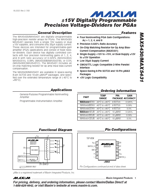
MAX5430 toc06
DIVIDER RATIO ACCURACY (%)
±15V Digitally Programmable Precision Voltage-Dividers for PGAs
Typical Operating Characteristics
(VDD = +15V, VSS = -15V or VSS = GND, VH = 5V, VL =-5V, TA = 25°C, unless otherwise noted.) (Note 3)
CIN
5
pF
POWER REQUIREMENTS
Negative Supply CurrentµA
Positive Supply Current
IDD
35
60
µA
Positive Power-Supply Voltage
VDD
Negative Power-Supply Voltage
VSS
10.8 -15.75
15.75
V
0
V
DYNAMIC PERFORMANCE
Switching Time
tD2W, tH2W
0.3
µs
Note 1: All devices are 100% production tested at TA = +25°C. SOT23 packages are guaranteed by design from TA = TMIN to TMAX. Note 2: Gain accuracy is measured without load at pin W.
Features
♦ Four Noninverting PGA Gain Configurations: AV = 1, 2, 4, and 8
MAX490EESA+资料
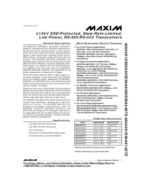
Supply Control
Voltage (VCC) Input Voltage
.(.–R—..E.–..,..D..E..)........................................-.0....5..V...t.o...(.V..C...C...+...0...152VV)
♦ For Low-Voltage Applications: MAX3483E/MAX3485E/MAX3486E/MAX3488E/ MAX3490E/MAX3491E: +3.3V Powered, ±15kV ESD-Protected, 12Mbps, Slew-Rate-Limited, True RS-485/RS-422 Transceivers
General Description
The MAX481E, MAX483E, MAX485E, MAX487E– MAX491E, and MAX1487E are low-power transceivers for RS-485 and RS-422 communications in harsh environments. Each driver output and receiver input is protected against ±15kV electro-static discharge (ESD) shocks, without latchup. These parts contain one driver and one receiver. The MAX483E, MAX487E, MAX488E, and MAX489E feature reduced slew-rate drivers that minimize EMI and reduce reflections caused by improperly terminated cables, thus allowing error-free data transmission up to 250kbps. The driver slew rates of the MAX481E, MAX485E, MAX490E, MAX491E, and MAX1487E are not limited, allowing them to transmit up to 2.5Mbps.
- 1、下载文档前请自行甄别文档内容的完整性,平台不提供额外的编辑、内容补充、找答案等附加服务。
- 2、"仅部分预览"的文档,不可在线预览部分如存在完整性等问题,可反馈申请退款(可完整预览的文档不适用该条件!)。
- 3、如文档侵犯您的权益,请联系客服反馈,我们会尽快为您处理(人工客服工作时间:9:00-18:30)。
19-1082; Rev 2; 12/99
+5V, Serial-Input, Voltage-Output, 16-Bit DACs
General Description
The MAX541/MAX542 are serial-input, voltage-output, 16-bit digital-to-analog converters (DACs) that operate from a single +5V supply. They provide 16-bit performance (±1LSB INL and DNL) over temperature without any adjustments. The DAC output is unbuffered, resulting in a low supply current of 0.3mA and a low offset error of 1LSB. The DAC output range is 0V to VREF. For bipolar operation, matched scaling resistors are provided in the MAX542 for use with an external precision op amp (such as the MAX400), generating a ±V REF output swing. The MAX542 also includes Kelvin-sense connections for the reference and analog ground pins to reduce layout sensitivity. A 16-bit serial word is used to load data into the DAC latch. The 10MHz, 3-wire serial interface is compatible with SPI™/QSPI™/MICROWIRE™, and it also interfaces directly with optocouplers for applications requiring isolation. A power-on reset circuit clears the DAC output to 0V (unipolar mode) when power is initially applied. The MAX541 is available in 8-pin plastic DIP and SO packages. The MAX542 is available in 14-pin plastic DIP and SO packages. o +5V Single-Supply Operation o Low Power: 1.5mW o 1µs Settling Time o Unbuffered Voltage Output Directly Drives 60kΩ Loads o SPI/QSPI/MICROWIRE-Compatible Serial Interface o Power-On Reset Circuit Clears DAC Output to 0V (unipolar mode) o Schmitt Trigger Inputs for Direct Optocoupler Interface
ELECTRICAL CHARACTERISTICS
(VDD = +5V ±5%, VREF = +2.5V, AGND = DGND = 0, TA = TMIN to TMAX, unless otherwise noted.) PARAMETER SYMBOL CONDITIONS MIN 16 MAX54_A Integral Nonlinearity Differential Nonlinearity Zero-Code Offset Error Zero-Code Tempco Gain Error (Note 1) Gain-Error Tempco DAC Output Resistance Bipolar Resistor Matching Bipolar Zero Offset Error Bipolar Zero Tempco Power-Supply Rejection REFERENCE INPUT Reference Input Range Reference Input Resistance (Note 4) BZSTC PSR VREF RREF ROUT (Note 2) MAX542 MAX542 MAX542 4.75V ≤ VDD ≤ 5.25V (Note 3) Unipolar mode MAX542, bipolar mode 2.0 11.5 9.0 25 1 RFB/RINV Ratio error TA = +25°C TA = TMIN to TMAX ±0.5 ±1.0 3.0 INL DNL ZSE ZSTC VDD = 5V Guaranteed monotonic TA = +25°C TA = TMIN to TMAX TA = TMIN to TMAX TA = +25°C TA = TMIN to TMAX ±0.1 6.25 1.0 ±0.015 ±10 ±20 % LSB ppm/°C LSB V kΩ ±0.05 ±5 ±10 MAX54_B MAX54_C ±0.5 ±0.5 ±0.5 ±0.5 ±1.0 ±2.0 ±4.0 ±1.0 ±1 ±2 LSB LSB ppm/°C LSB ppm/°C kΩ LSB TYP MAX UNITS Bits STATIC PERFORMANCE—ANALOG SECTION (RL = ∞) Resolution N
+5V, Serial-Input, Voltage-Output, 16-Bit DACs MAX541/MAX542
ABSOLUTE MAXIMUM RATINGS
VDD to DGND ...........................................................-0.3V to +6V CS, SCLK, DIN, LDAC to DGND ..............................-0.3V to +6V REF, REFF, REFS to AGND ........................-0.3V to (VDD + 0.3V) AGND, AGNDF, AGNDS to DGND........................-0.3V to +0.3V OUT, INV to AGND, DGND ......................................-0.3V to VDD RFB to AGND, DGND..................................................-6V to +6V Maximum Current into Any Pin............................................50mA Continuous Power Dissipation (TA = +70°C) 8-Pin Plastic DIP (derate 9.09mW/°C above +70°C) .....727mW 8-Pin SO (derate 5.88mW/°C above +70°C) .................471mW 14-Pin Plastic DIP (derate 10.00mW/°C above +70°C) ...800mW 14-Pin SO (derate 8.33mW/°C above +70°C) ...............667mW 14-Pin Ceramic SB (derate 10.00mW/°C above +70°C ..800mW Operating Temperature Ranges MAX541 _C_ A/MAX542_C_D. .............................0°C to +70°C MAX541 _E_ A/MAX542_E_D............................-40°C to +85°C MAX542CMJD .................................................-55°C to +125°C Storage Temperature Range .............................-65°C to +150°C Lead Temperature (soldering, 10s) .................................+300°C
AGNDF 3 AGNDS 4 REFS 5
MAX542
12 DGND 11 LDAC 10 DIN 9 N.C. 8 SCLK
REFF 6 CS 7
CS LDAC SCLK DIN
16-BIT DATA LATCH CONTROL LOGIC SERIAL INPUT REGISTER DGND
Applications
High-Resolution Offset and Gain Adjustment Industrial Process Control Automated Test Equipment Data-Acquisition Systems
Ordering Information continued at end of data sheet.