4171300XX-3, 规格书,Datasheet 资料
PI3B3257 Datasheet说明书

VIN = 0V
CON
IN/YN Capacitance, Switch ON
Notes:
1. This parameter is determined by device characterization but is not production tested.
Typ.
Units
3.0
17.0
pF
Parameters Description
Test Conditions(1)
Min. Typ.(2) Max. Units
VIH
Input HIGH Voltage
VIL
Input LOW Voltage
Guaranteed Logic HIGH Level
2
Guaranteed Logic LOW Level
generate no significant AC or DC currents as they transition. This parameter is not tested, but is guaranteed by design.
VIK
Clamp Diode Voltage
VCC = Min., IIN = –18mA
–1.2
V
VCC = Min., VIN = 0.0V,
RON
Switch On-Resistance(3)
Ion = 48mA or 64mA
VCC = Min., VIN = 2.4V, ION = 15mA
Note: Stresses greater than those listed under MAXIMUM RATINGS may cause permanent damage to the device. This is a stress rating only and functional operation of the device at these or any other conditions above those indicated in the operational sections of this specification is not mplied. Exposure to absolute maximum rating conditions for extended periods may affect reliability.
ams 4173标准
ams 4173标准摘要:1.AMS 4173 标准的概述2.AMS 4173 标准的主要内容3.AMS 4173 标准的应用领域4.AMS 4173 标准的重要性正文:AMS 4173 标准是由美国材料和试验协会(ASTM)制定的一种标准,全称为“Standard Specification for Tungsten and Tungsten Alloy Bars and Wires”,即“钨和钨合金棒和线材的标准规格”。
这个标准主要规定了钨和钨合金棒和线材的尺寸、形状、允许偏差、表面光洁度、机械性能、化学成分等技术要求。
AMS 4173 标准的主要内容包括:1.尺寸和形状:标准规定了钨和钨合金棒和线材的直径、长度、方形度、圆度等尺寸和形状要求。
2.允许偏差:标准规定了钨和钨合金棒和线材的壁厚、直径、长度等允许偏差。
3.表面光洁度:标准规定了钨和钨合金棒和线材的表面光洁度要求,包括表面粗糙度、光泽等。
4.机械性能:标准规定了钨和钨合金棒和线材的拉伸强度、屈服强度、硬度等机械性能要求。
5.化学成分:标准规定了钨和钨合金棒和线材的化学成分要求,包括钨、铜、银、镍等元素的含量。
AMS 4173 标准的应用领域非常广泛,主要应用于航空航天、军事、核能、电子、化工等高技术领域。
例如,钨合金棒和线材可以作为航空航天发动机的高温部件,也可以作为核能反应堆的控制棒,还可以作为电子器件的焊接材料等。
AMS 4173 标准的重要性不言而喻。
首先,这个标准为钨和钨合金棒和线材的生产和检验提供了一个统一的技术规范,保证了产品的质量和可靠性。
其次,这个标准有助于提高钨和钨合金棒和线材的生产效率和经济效益,降低了生产成本。
最后,这个标准有助于推动钨和钨合金棒和线材的技术进步和创新,促进了新材料、新工艺、新技术的发展。
MAX4173TEUT-T中文资料

Notebook Computers
Portable/Battery-Powered Systems
Smart Battery Packs/Chargers
Cell Phones
Power-Management Systems
General System/Board-Level Current Monitoring
The combination of three gain versions and a userselectable external sense resistor sets the full-scale current reading. This feature offers a high level of integration, resulting in a simple and compact currentsense solution.
+20V/V (MAX4173T) +50V/V (MAX4173F) +100V/V (MAX4173H) ♦ ±0.5% Full-Scale Accuracy ♦ ±0.3mV Input Offset Voltage (MAX4173T) ♦ 420µA Supply Current ♦ Wide 1.7MHz Bandwidth (MAX4173T) ♦ +3V to +28V Operating Supply ♦ Available in Space-Saving SOT23-6 Package
Typical Operating Circuit
0 TO +28V
VSENSE
+3V TO +28V 0.1µF
某地区某公司对讲电气cad设计图
A3177中文资料
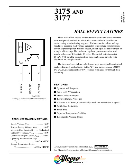
These Hall-effect latches are temperature-stable and stress-resistant sensors especially suited for electronic commutation in brushless dc motors using multipole ring magnets. Each device includes a voltage regulator, quadratic Hall voltage generator, temperature compensation circuit, signal amplifier, Schmitt trigger, and an open-collector output on a single silicon chip. The on-board regulator permits operation with supply voltages of 4.5 volts to 18 volts. The switch output can sink 10 mA. With suitable output pull up, they can be used directly with bipolar or MOS logic circuits.The three package styles available provide a magnetically optimized package for most applications. Suffix ‘LT’ is a surface-mount SOT89/TO-243AA package; suffixe ‘UA’ features wire leads for through-hole mounting.HALL-EFFECT LATCHESAlways order by complete part number, e.g., UGN3175LT .See Magnetic Characteristics table for differences between devices.Data Sheet27609.4CFEATURESs Symmetrical Response s 4.5 V to 18 V Operation s Open-Collector Output s Reverse Battery Protections Activate With Small, Commercially Available Permanent Magnets s Solid-State Reliability s Small Sizes Superior Temperature Stability s Resistant to Physical Stress3175 AND 3177115 Northeast Cutoff, Box 15036Worcester, Massachusetts 01615-0036 (508) 853-5000NOTE:As used here, negative flux densities are defined as less than zero (algebraic convention).Complete part number includes a suffix denoting package type (LT or UA).T A = +25°CT A = -20°C to +85°CCharacteristic Min.Typ.Max.Min.Typ.Max.Operate Point, B OPUGN317525—17015—180UGN317750—15025—150Release Point, B RPUGN3175-170—-25-180—-15UGN3177-150—-50-150—-25Hysteresis, B hysUGN3175100200—80180—UGN3177100200—50180—Part Number*MAGNETIC CHARACTERISTICS in gauss; V CC = 4.5 V to 18 V.Copyright © 1991, 2002 Allegro MicroSystems, Inc.TYPICAL OPERATING CHARACTERISTICSSuffix “UA”-10103050AMBIENT TEMPERATURE IN °C-30Dwg. GH-020S W I T C H P O I N T I N G A U S S100200-100-200Dwg. MH-011CSuffix “LT”Dwg. MH-008-1C0.0305"NOMSENSOR LOCATIONS(±0.005” [0.13mm] die placement)The products described herein are manufactured under one or more of the following U.S. patents: 5,045,920; 5,264,783; 5,442,283;5,389,889; 5,581,179; 5,517,112; 5,619,137; 5,621,319; 5,650,719;5,686,894; 5,694,038; 5,729,130; 5,917,320; and other patents pending.Allegro MicroSystems, Inc. reserves the right to make, from time to time, such departures from the detail specifications as may berequired to permit improvements in the performance, reliability, or manufacturability of its products. Before placing an order, the user is cautioned to verify that the information being relied upon is current.Allegro products are not authorized for use as critical components in life-support appliances, devices, or systems without express written approval.The information included herein is believed to be accurate and reliable. However, Allegro MicroSystems, Inc. assumes no responsi-bility for its use; nor for any infringements of patents or other rights of third parties that may result from its use.115 Northeast Cutoff, Box 15036Worcester, Massachusetts 01615-0036 (508) 853-5000PACKAGE DESIGNATOR ‘LT’(SOT89/TO-243AA)Dimensions in Inches (for reference only)Dimensions in Millimeters (controlling dimensions)NOTES: 1.Exact body and lead configuration at vendor’s option within limits shown.2.Supplied in bulk pack (500 pieces per bag) or add "TR" to part number for tape and reel.3.Only low-temperature (≤240°C) reflow-soldering techniques are recommended for SOT89 devices.0.440.35Dwg. MA-012-3 inPads 1, 2, 3, and B — Low-Stress VersionPads 1, 2, and 3 only — Lowest Stress, But Not Self AligningDwg. MA-012-3 mmPads 1, 2, 3, and B — Low-Stress VersionPads 1, 2, and 3 only — Lowest Stress, But Not Self AligningDimensions in Inches (controlling dimensions)Dimensions in Millimeters(for reference only)PACKAGE DESIGNATOR ‘UA’NOTES: 1.Tolerances on package height and width representallowable mold offsets. Dimensions given are measured at the widest point (parting line).2.Exact body and lead configuration at vendor’s optionwithin limits shown.3.Height does not include mold gate flash.4.Recommended minimum PWB hole diameter to cleartransition area is 0.035" (0.89 mm).5.Where no tolerance is specified, dimension is nominal.6.Supplied in bulk pack (500 pieces per bag).Dwg. MH-014E in0.050BSC°Dwg. MH-014E mm1.27BSC°Radial Lead Form (order A317xxUA-LC)NOTE:Lead-form dimensions are the nominals produced on theforming equipment. No dimensional tolerance is implied or guaranteed for bulk packaging (500 pieces per bag).(2.5 mm)Dwg. MH-026115 Northeast Cutoff, Box 15036Worcester, Massachusetts 01615-0036 (508) 853-5000HALL-EFFECT SENSORSUNIPOLAR HALL-EFFECT DIGITAL SWITCHESPartial Operate Release Hysteresis Replaces Part Point (G)Point (G)(G)Oper.and Number Over Oper. Voltage & Temp. Range Temp.PackagesCommentsA3121x 220 to 50080 to 41060 to 150E, L LT, UA 3019, 3113, 3119A3122x 260 to 430120 to 36070 to 140E, L LT, UA A3123x 230 to 470160 to 33070 to 140E, L LT, UA A3141x 30 to 17510 to 14520 to 80E, L LT, UA 3040, 3140A3142x 115 to 24560 to 19030 to 80E, L LT, UA A3143x 205 to 355150 to 30030 to 80E, L LT, UA A3144x 35 to 45025 to 430>20E, L LT, UA 3020, 3120A3161E <160 (Typ 130)>30 (Typ 110) 5 to 80E LT, UA 2-wire operation A3163E <160 (Typ 98)>30 (Typ 79) 5 to 40E LT, UA 2-wire A3240x <50 (Typ 35)>5 (Typ 25)Typ 10E, L LH, LT, UA chopper stabilizedA3250x <50 to >350_ 5 to 35J, L UA programmable, chopper stabilized A3251x <50 to >350_5 to 35J, L UA programmable, chopper stabilizedA3361E <125>40 5 to 30E LH, LT, UA2-wire, chopper stabilized,output normally high A3362E<125>405 to 30ELH, LT, UA2-wire, chopper stabilized,output normally lowMICROPOWER OMNIPOLAR HALL-EFFECT DIGITAL SWITCHESPartial Operate Release Hysteresis Average Part Points (G)Points (G)(G)Oper.Supply Number Over Oper. Voltage & Temp. Range Temp.Packages Current (µA)A3209E >-60, <60<-5, >5Typ 7.7E LH, UA <425 (Typ 145)A3210E >-60, <60<-5, >5Typ 7.7E LH, UA <60 (Typ 8.8)A3212E>-55, <55<-10, >10Typ. 8ELH, UA<10 (Typ 4.2)BIPOLAR HALL-EFFECT DIGITAL SWITCHESPartial Operate Release Hysteresis Replaces Part Point (G)Point (G)(G)Oper.and Number Over Oper. Voltage & Temp. Range Temp.Packages Comments UGx3132<95 (Typ 32)>-95 (Typ -20)>30 (Typ 52)K, L, S LT, UA 3030, 3130, 3131UGx3133<75 (Typ 32)>-75 (Typ -20)>30 (Typ 52)K, L, S LT, UA UGx3134-40 to 50-50 to 40 5 to 55E, L LT, UA A3260x<30 (Typ 10)>-30 (Typ -10)Typ 20E, LLH, LT, UA2 wire, chopper stabilizedNotes:1) Typical data is at T A = +25°C and nominal operating voltage.2) “x” = Operating Temperature Range [suffix letter or (prefix)]: S (UGN) = -20°C to +85°C, E = -40°C to +85°C,J = -40°C to +115°C, K (UGS) = -40°C to +125°C, L (UGL) = -40°C to +150°C.。
电源管理芯片AXP173 Datasheet
17H
38H
9.10 Host接口及中断(Host Interface and IRQ)................................................................................... 27
18H
39H
9.11 寄存器(Registers) ............................................................................................................................. 28
7.管脚定义(Pin Description)....................................................................................................................... 13
6H
27H
8.功能框图(Functional Block Diagram).................................................................................................. 15
TCST1103;TCST1300;中文规格书,Datasheet资料

Transmissive Optical Sensor with Phototransistor OutputDESCRIPTIONThe TCST1103, TCST1202, and TCST1300 are transmissive sensors that include an infrared emitter and phototransistor,located face-to-face on the optical axes in a leaded package which blocks visible light. These part numbers include options for aperture width.FEATURES•Package type: leaded •Detector type: phototransistor•Dimensions (L x W x H in mm): 11.9 x 6.3 x 10.8•Gap (in mm): 3.1•Typical output current under test: I C = 4 mA (TCST1103)•Typical output current under test: I C = 2 mA (TCST1202)•Typical output current under test: I C = 0.5 mA (TCST1300)•Daylight blocking filter •Emitter wavelength: 950 nm •Lead (Pb)-free soldering released•Compliant to RoH S Directive 2002/95/EC and in accordance to WEEE 2002/96/ECAPPLICATIONS•Optical switch •Photo interrupter •Counter •EncoderNote•Conditions like in table basic characteristics/couplerNote•MOQ: minimum order quantity19180_5PRODUCT SUMMARYPART NUMBER GAP WIDTH(mm)APERTURE WIDTH(mm)TYPICAL OUTPUT CURRENTUNDER TEST (1)(mA)DAYLIGHT BLOCKING FILTER INTEGRATEDTCST1103 3.114Yes TCST1202 3.10.52Yes TCST13003.10.250.5YesORDERING INFORMATIONORDERING CODE PACKAGINGVOLUME (1)REMARKS TCST1103Tube MOQ: 1020 pcs, 85 pcs/tube Without mounting flange TCST1202Tube MOQ: 1020 pcs, 85 pcs/tube Without mounting flange TCST1300TubeMOQ: 1020 pcs, 85 pcs/tubeWithout mounting flangeABSOLUTE MAXIMUM RATINGS (T amb = 25 °C, unless otherwise specified)PARAMETER TEST CONDITIONSYMBOLVALUEUNITCOUPLERTotal power dissipation T amb ≤ 25 °CP tot 250mW Ambient temperature range T amb - 55 to + 85°C Storage temperature range T stg - 55 to + 100°C Soldering temperatureDistance to package: 2 mm; t ≤ 5 sT sd260°CABSOLUTE MAXIMUM RATINGSFig. 1 - Power Dissipation Limit vs. Ambient TemperatureINPUT (EMITTER)Reverse voltage V R 6V Forward current I F60mA Forward surge current t p ≤ 10 μs I FSM 3A Power dissipation T amb ≤ 25 °CP V 100mW Junction temperature T j 100°C OUTPUT (DETECTOR)Collector emitter voltage V CEO 70V Emitter collector voltage V ECO7V Collector peak current t p /T = 0.5, t p ≤ 10 msI CM 200mA Power dissipation T amb ≤ 25 °CP V 150mW Junction temperatureT j100°CABSOLUTE MAXIMUM RATINGS (T amb = 25 °C, unless otherwise specified)PARAMETER TEST CONDITIONSYMBOLVALUE UNIT BASIC CHARACTERISTICS (T amb = 25 °C, unless otherwise specified)PARAMETER TEST CONDITIONPARTSYMBOLMIN.TYP.MAX.UNITCOUPLERCurrent transfer ratioV CE = 5 V, I F = 20 mATCST1103CTR 1020%TCST1202CTR 510%TCST1300CTR 1.25 2.5%Collector currentV CE = 5 V, I F = 20 mA TCST1103I C 24mA TCST1202I C 12mA TCST1300I C 0.250.5mA Collector emitter saturationvoltageI F = 20 mA, I C = 1 mA TCST1103V CEsat 0.4V I F = 20 mA, I C = 0.5 mA TCST1202V CEsat 0.4V I F = 20 mA, I C = 0.1 mA TCST1300V CEsat 0.4V Resolution, path of the shutter crossing the radiant sensitive zoneI Crel = 10 % to 90 %TCST1103s 0.6mm TCST1202s 0.4mm TCST1300s0.2mmFig. 2 - Test Circuit for t on and t offFig. 3 - Switching TimesBASIC CHARACTERISTICS (T amb = 25 °C, unless otherwise specified)Fig. 4 - Forward Current vs. Forward Voltage Fig. 5 - Relative Current Transfer Ratio vs. Ambient TemperatureINPUT (EMITTER)Forward voltage I F = 60 mA V F 1.25 1.6V Junction capacitance V R = 0 V, f = 1 MHzC j50pFOUTPUT (DETECTOR)Collector emitter voltage I C = 1 mA V CEO 70V Emitter collector voltage I E = 10 μAV ECO 7V Collector dark currentV CE = 25 V, I F = 0 A, E = 0 lxI CEO100nASWITCHING CHARACTERISTICS Turn-on time I C = 2 mA, V S = 5 V,R L = 100 Ω (see figure 2)t on 10μs Turn-off timeI C = 2 mA, V S = 5 V,R L = 100 Ω (see figure 2)t off8μsBASIC CHARACTERISTICS (T amb = 25 °C, unless otherwise specified)PARAMETER TEST CONDITIONPARTSYMBOLMIN.TYP.MAX.UNIT10 %90 %100 %I F I C t p Pulse duration t d Delay time t rRise time t on (= t d + t r )Turn-on timet s Storage time t fFall time t off (= t s+ t f )Turn-off time96 11698Fig. 6 - Collector Dark Current vs. Ambient Temperature Fig. 7 - Collector Current vs. Forward CurrentFig. 8 - Collector Current vs. Collector Emitter VoltageFig. 9 - Current Transfer Ratio vs. Forward Current Fig. 10 - Turn-off/Turn-on Time vs. Collector Current Fig. 11 - Relative Collector Current vs. DisplacementFig. 12 - Relative Collector Current vs. Displacement Fig. 13 - Relative Collector Current vs. DisplacementPACKAGE DIMENSIONS in millimetersTUBE DIMENSIONS in millimetersDocument Number: 80112For technical questions, contact: optocoupleranswers@Packaging and Ordering InformationPackaging and Ordering InformationVishay SemiconductorsNotes(1)MOQ: minimum order quantity (2)Please refer to datasheetsTUBE SPECIFICATION FIGURESFig. 1PART NUMBER MOQ (1)PCS PER TUBETUBE SPEC.(FIGURE)CONSTITUENTS(FORMS)CNY70400080128TCPT1300X012000Reel (2)29TCRT10001000Bulk -26TCRT10101000Bulk -26TCRT5000450050227TCRT5000L 240048327TCST1030520065524TCST1030L 260065624TCST1103102085424TCST1202102085424TCST1230480060724TCST1300102085424TCST2103102085424TCST2202102085424TCST2300102085424TCST5250486030824TCUT1300X012000Reel (2)29TCZT8020-PAER2500Bulk-22Packaging and Ordering InformationVishay Semiconductors Packaging and Ordering InformationFig. 2Fig. 3 For technical questions, contact: optocoupleranswers@ Document Number: 80112Packaging and Ordering InformationPackaging and Ordering Information Vishay SemiconductorsFig. 4Fig. 5Document Number: 80112For technical questions, contact: optocoupleranswers@ Packaging and Ordering InformationVishay Semiconductors Packaging and Ordering InformationFig. 6Fig. 7 For technical questions, contact: optocoupleranswers@ Document Number: 80112分销商库存信息:VISHAYTCST1103TCST1300。
(参考资料)HJ30J产品样本

绿
1
1#
白绿
20
白
21
橙
19
2#
白橙
2
白
3
蓝
4
3#
白蓝
23
白
24
棕
22
4#
白棕
5
白
6
绿
7
5#
白绿
26
白
27
橙
25
6#
白橙
8
白
9
蓝
10
7#
白蓝
29
白
30
棕
28
8#
白棕
11
白
12
绿
13
9#
白绿
32
白
33
橙
31
10 #
白橙
14
白
15
蓝
16
11 #
白蓝
35
白
36
棕
34
12 #
白棕
17
白
18
4
55芯 导线 颜色 、连接 器孔 位及 热缩 后线 束编 号对 应表
线 束标 识
导线颜色 连接器孔位编号
绿
1
1#
白绿
14
白
15
橙
13
2#
白橙
2
白
3
蓝
4
3#
白蓝
17
白
18
棕
16
4#
白棕
5
白
6
绿
7
5#
白绿
20
白
21
橙
19
6#
白橙
8
白
9
蓝
美国ASTM的不锈钢标准标_准体系和牌号概述
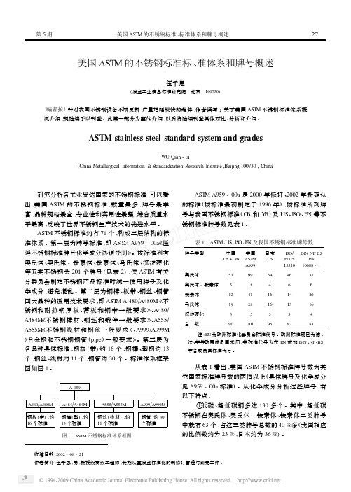
研究分析各工业发达国家的不锈钢标准 ,可以看 出 ,美国 ASTM 的不锈钢标准 ,数量最多 ,牌号最丰 富 ,品种规格最全 ,专业性和实用性最强 ,综合质量水 平最高 ,反映了世界不锈钢生产技术的先进水平 。
ASTM 不锈钢标准约有 71 个 ,构成三层结构的标 准体系 。第一层为牌号标准 ,即 ASTM A959 - 00《a 压 延不锈钢标准牌号化学成分协调导则》。该标准列有 奥氏体 、奥氏体 - 铁素体 、铁素体 、马氏体 、沉淀硬化 等五类不锈钢共 201 个牌号 (见表 2) ,供 ASTM 有关 分委员会制定不锈钢产品标准时统一使用牌号及化 学成分 ,避免混乱 。第二层为钢棒 、板带 、钢丝 、钢管 四大品种的通用技术要求 ,即 ASTM A 480ΠA480M《不 锈钢和耐 热 钢 厚 板 、薄 板 和 钢 带 一 般 要 求》、A480Π A484M《不锈钢棒材 、钢坯和锻件一般要求》、A555Π A555M《不 锈 钢 线 材 和 钢 丝 一 般 要 求 》、A999ΠA999M 《合金钢和不锈钢钢管 (pipe) 一般要求》。第三层为 各品种具体标准 ,钢板 (带) 约 16 个 ,钢棒 、型钢约 13 个 ,钢丝 、线材约 11 个 ,钢管约 30 个 。标准体系框架 图如图 1 。
①低碳 、超低碳钢多达 130 多个 。其中 ,超低碳 不锈钢在奥氏体 、奥氏体 - 铁素体 、铁素体三类牌号 中就有 63 个 ,占这三类牌号总数的 40 %多 (我国相应 的比例数约为 23 % ,日本约为 36 %) 。
收稿日期 :2002 - 08 - 21 作者简介 :伍千思 ,男 ,教授级高级工程师 ,长期从事冶金标准化的制修订管理与研究工作 。
ISOΠTR 10013 是由 ISOΠTC 176ΠSC3ΠWG9 国际标 准化组织质量管理和质量保证技术委员会第 3 分委 员会第 9 工作组制定的 ,他们根据 ISO 9000 :2000 族 国际标准要求制定质量管理体系 (QMS) ,并根据改善 其功效时采用的程序方法和质量管理体系的文件编 制要求制定了该指南 ,TR 10013 明显提升了程序文件 编制方法 。
1N4007规格书
C
VR=-4VDC
15
ΡF
6.额定值曲线特性
23.4Min4.2~5.223.4 Min
主要材料/电镀
铜/镀锡( 7μmto 9μm)
2.印字
1. 阴极标志
2.型号名字1N4007
3. 数据标码WY
3.编带规格及包装
包装
KK
ΔS
SK:1.0mm
S:10.0±0.5mm
BΔS:1.2mm
B:6.0±1.0mm
GG:43.4±1.5mm
包装散装(非编带)1N4007-T
最大额定值内容符号额定单位最大反向电压vrrm1000v最大正向平均电流最大浪涌电流储存温度ifavifsm10aa300tjtstg651255
1N4007产品规格书
目录:
1.封装尺寸
2.印字
3.编带规格及包装
4.最大额定值
5.电性能参数
6.额定值曲线特性
张家港伟益电子有限公司
1.封装尺寸
φ0.6~0.7φ2.0~2.7
4.最大额定值
内容
符号
ห้องสมุดไป่ตู้额定
单位
最大反向电压
VRRM
1000
V
最大正向平均电流
IF(AV)
1.0
A
最大浪涌电流
IFSM
30.0
A
储存温度
Tj, Tstg
-65~+125
℃
5.电性能参数
内容
符号
条件
最大
单位
最大正向电压
VFM
IFM=1A
1.1
V
最大反向电流
IRRM
VTM=Rated Voltage
5
uA
744770133;中文规格书,Datasheet资料
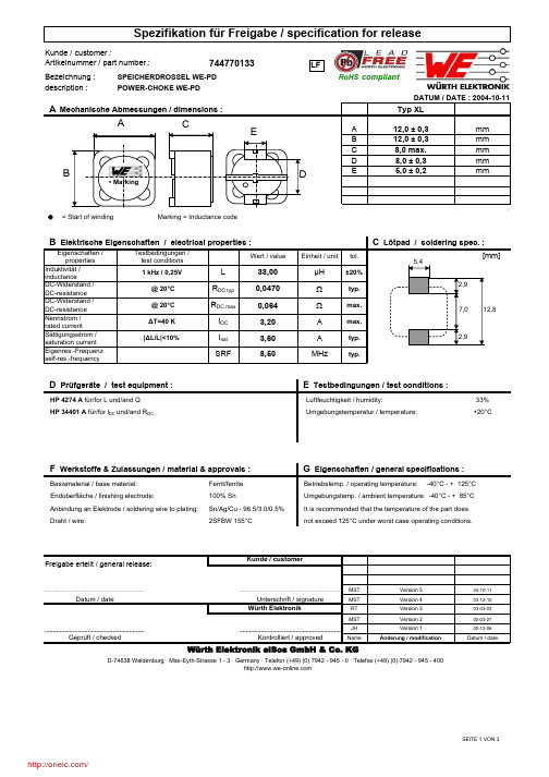
Bezeichnung :description := Start of winding Marking = Inductance code33% Umgebungstemperatur / temperature:+20°C100% SnMST 04-10-11MST 03-12-10RT 03-03-03MST02-03-27JH 00-12-06NameDatum / dateIt is recommended that the temperature of the part does not exceed 125°C under worst case operating conditions.Anbindung an Elektrode / soldering wire to plating:Sn/Ag/Cu - 96.5/3.0/0.5%Draht / wire:2SFBW 155°CUmgebungstemp. / ambient temperature: -40°C - + 85°C Freigabe erteilt / general release:Kunde / customerWürth Elektronik....................................................................................................................................................................Unterschrift / signature Ferrit/ferrite F Werkstoffe & Zulassungen / material & approvals :G Eigenschaften / general specifications :D Prüfgeräte / test equipment :E Testbedingungen / test conditions :Basismaterial / base material:Betriebstemp. / operating temperature: -40°C - + 125°C D-74638 Waldenburg · Max-Eyth-Strasse 1 - 3 · Germany · Telefon (+49) (0) 7942 - 945 - 0 · Telefax (+49) (0) 7942 - 945 - 400Geprüft / checked ..........................................................................................................................Kontrolliert / approvedWürth Elektronik eiSos GmbH & Co. KG744770133SPEICHERDROSSEL WE-PDPOWER-CHOKE WE-PDArtikelnummer / part number : Luftfeuchtigkeit / humidity:HP 4274 A für/for L und/and Q HP 34401 A für/for I DC und/and R DCÄnderung / modificationVersion 1Version 2Version 3Version 4Version 5 Datum / dateEndoberfläche / finishing electrode:• MarkingRoHS compliantLFdescription :MST 04-10-11MST 03-12-10RT 03-03-03MST02-03-27JH 00-12-06NameDatum / dateH Induktivitätskurve / Inductance curve :POWER-CHOKE WE-PDDATUM / DATE : 2004-10-11Kontrolliert / approvedDatum / dateUnterschrift / signature Würth ElektronikWürth Elektronik eiSos GmbH & Co. KGD-74638 Waldenburg · Max-Eyth-Strasse 1 - 3 · Germany · Telefon (+49) (0) 7942 - 945 - 0 · Telefax (+49) (0) 7942 - 945 - 400Freigabe erteilt / general release:Kunde / customer..................................................................................................................................................................................................................................................................................Geprüft / checked Version 4Version 5Änderung / modificationVersion 1Version 2Version 3a 330,0± 0,5mmb 20,20± 0,2mm+ 0,5- 1,0d 100,0± 0,2mmMST 04-10-11MST 03-12-10RT 03-03-03MST02-03-27JH 00-12-06NameDatum / dateRollenspezifikation / Reel specification:Freigabe erteilt / general release:Kunde / customerc 13,00mm....................................................................................................................................................................Datum / dateUnterschrift / signature Würth Elektronik..........................................................................................................................Würth Elektronik eiSos GmbH & Co. KGGeprüft / checked Kontrolliert / approvedD-74638 Waldenburg · Max-Eyth-Strasse 1 - 3 · Germany · Telefon (+49) (0) 7942 - 945 - 0 · Telefax (+49) (0) 7942 - 945 - 400Änderung / modificationVersion 1Version 2Version 3Version 4Version 5The force for tearing off cover tape is 10 to 130 grams in arrow direction165 to 180°feeding directionThis electronic component is designed and developed with the intention for use in general electronics equipments. Before incorporating the components into any equipments in the field such as aerospace, aviation, nuclear control, submarine, transportation, (automotive control, train control, ship control), transportation signal, disaster prevention, medical, public information network etc. where higher safety and reliability are especially required or if there is possibility of direct damage or injury to human body. In addition, even electronic component in general electronic equipments, when used in electrical circuits that require high safety, reliability functions or performance, the sufficient reliability evaluation-check for the safety must be performed before use. It is essential to give consideration when to install a protective circuit at the design stage.分销商库存信息: WURTH-ELECTRONICS 744770133。
744373240047;中文规格书,Datasheet资料
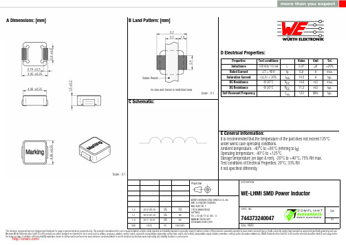
1.2 1.1 1.02012-06-282012-02-292011-10-01SStSStSStSStBDBDWürth Elektronik eiSos GmbH & Co. KGEMC & Inductive SolutionsMax-Eyth-Str. 174638 WaldenburgGermanyTel. +49 (0) 79 42 945 - 0A Dimensions: [mm]F Typical Inductance vs. Current Characteristics: F Typical Temperature rise vs. Current Characteristics:H1: Classification Reflow Profile for SMT components:H2: Classification Reflow ProfilesProfile FeaturePreheat- Temperature Min (T smin ) - Temperature Max (T smax ) - Time (t s ) from (T smin to T smax )Ramp-up rate (T L to T P )Liquidous temperature (T L )Time (t L ) maintained above T L Peak package body temperature (T p )Time within 5°C of actual peak temperature (t p )Ramp-down rate (T P to T L )Time 25°C to peak temperature Pb-Free Assembly 150°C 200°C60-180 seconds 3°C/ second max.217°C60-150 seconds See Table H320-30 seconds 6°C/ second max.8 minutes max.refer to IPC/JEDEC J-STD-020DH3: Package Classification Reflow TemperaturePB-Free Assembly PB-Free Assembly PB-Free Assembly Package Thickness< 1.6 mm 1.6 - 2.5 mm ≥ 2.5 mmVolume mm³<350260°C 260°C 250°CVolume mm³350 - 2000260°C 250°C 245°CVolume mm³>2000260°C 245°C 245°Crefer to IPC/JEDEC J-STD-020DH Soldering Specifications:I Cautions and Warnings:The following conditions apply to all goods within the product series of WE-LHMIof Würth Elektronik eiSos GmbH & Co. KG:General:All recommendations according to the general technical specifications of the data-sheet have to be complied with.The disposal and operation of the product within ambient conditions which probably alloy or harm the wire isolation has to be avoided.If the product is potted in customer applications, the potting material might shrink during and after hardening. Accordingly to this the product is exposed to the pressure of the potting material with the effect that the core, wire and termination is possibly damaged by this pressure and so the electrical as well as the mechanical characteristics are endanger to be affected. After the potting material is cured, the core, wire and termination of the product have to be checked if any reduced electrical or mechanical functions or destructions have occurred.The responsibility for the applicability of customer specific products and use in a particular customer design is always within the authority of the customer. All technical specifications for standard products do also apply for customer specific products.Washing varnish agent that is used during the production to clean the application might damage or change the characteristics of the wire in-sulation, the marking or the plating. The washing varnish agent could have a negative effect on the long turn function of the product.Direct mechanical impact to the product shall be prevented as the iron powder material of the core could flake or in the worst case it could break.Product specific:Follow all instructions mentioned in the datasheet, especially:•The solder profile has to be complied with according to the technical reflow soldering specification, otherwise no warranty will be sustai-ned.•All products are supposed to be used before the end of the period of 12 months based on the product date-code, if not a 100% solderabi-lity can´t be warranted.•Violation of the technical product specifications such as exceeding the nominal rated current will result in the loss of warranty.1. General Customer ResponsibilitySome goods within the product range of Würth Elektronik eiSos GmbH & Co. KG contain statements regarding general suitability for certain application areas. These statements about suitability are based on our knowledge and experience of typical requirements concerning the are-as, serve as general guidance and cannot be estimated as binding statements about the suitability for a customer application. The responsibi-lity for the applicability and use in a particular customer design is always solely within the authority of the customer. Due to this fact it is up to the customer to evaluate, where appropriate to investigate and decide whether the device with the specific product characteristics described in the product specification is valid and suitable for the respective customer application or not.2. Customer Responsibility related to Specific, in particular Safety-Relevant ApplicationsIt has to be clearly pointed out that the possibility of a malfunction of electronic components or failure before the end of the usual lifetime can-not be completely eliminated in the current state of the art, even if the products are operated within the range of the specifications.In certain customer applications requiring a very high level of safety and especially in customer applications in which the malfunction or failure of an electronic component could endanger human life or health it must be ensured by most advanced technological aid of suitable design of the customer application that no injury or damage is caused to third parties in the event of malfunction or failure of an electronic component.3. Best Care and AttentionAny product-specific notes, warnings and cautions must be strictly observed.4. Customer Support for Product SpecificationsSome products within the product range may contain substances which are subject to restrictions in certain jurisdictions in order to serve spe-cific technical requirements. Necessary information is available on request. In this case the field sales engineer or the internal sales person in charge should be contacted who will be happy to support in this matter.5. Product R&DDue to constant product improvement product specifications may change from time to time. As a standard reporting procedure of the Product Change Notification (PCN) according to the JEDEC-Standard inform about minor and major changes. In case of further queries regarding the PCN, the field sales engineer or the internal sales person in charge should be contacted. The basic responsibility of the customer as per Secti-on 1 and 2 remains unaffected.6. Product Life CycleDue to technical progress and economical evaluation we also reserve the right to discontinue production and delivery of products. As a stan-dard reporting procedure of the Product Termination Notification (PTN) according to the JEDEC-Standard we will inform at an early stage about inevitable product discontinuance. According to this we cannot guarantee that all products within our product range will always be available. Therefore it needs to be verified with the field sales engineer or the internal sales person in charge about the current product availability ex-pectancy before or when the product for application design-in disposal is considered.The approach named above does not apply in the case of individual agreements deviating from the foregoing for customer-specific products.7. Property RightsAll the rights for contractual products produced by Würth Elektronik eiSos GmbH & Co. KG on the basis of ideas, development contracts as well as models or templates that are subject to copyright, patent or commercial protection supplied to the customer will remain with Würth Elektronik eiSos GmbH & Co. KG.8. General Terms and ConditionsUnless otherwise agreed in individual contracts, all orders are subject to the current version of the “General Terms and Conditions of Würth Elektronik eiSos Group”, last version available at .J Important Notes:The following conditions apply to all goods within the product range of Würth Elektronik eiSos GmbH & Co. KG:分销商库存信息: WURTH-ELECTRONICS 744373240047。
DFLS1100-7;中文规格书,Datasheet资料
1.0A HIGH VOLTAGE SCHOTTKY BARRIER RECTIFIERPOWERDI ®123Features• Guard Ring Die Construction for Transient Protection • Low Power Loss, High Efficiency• Patented Interlocking Clip Design for High Surge Current Capacity• Lead Free Finish, RoHS Compliant (Note 1) • "Green" Molding Compound (No Br, Sb)• Qualified to AEC-Q101 Standards for High ReliabilityMechanical Data• Case: POWERDI ®123 • Case Material: Molded Plastic, “Green” Molding Compound.UL Flammability Classification Rating 94V-0 • Moisture Sensitivity: Level 1 per J-STD-020 • Terminal Connections: Cathode Band • Terminals: Finish – Matte Tin annealed over Copperleadframe. Solderable per MIL-STD-202, Method 208 • Weight: 0.01 grams (approximate)Ordering Information (Note 2)Part Number Case Packaging DFLS1100-7 POWERDI ®1233000/Tape & ReelNotes: 1. EU Directive 2002/95/EC (RoHS). All applicable RoHS exemptions applied, see EU Directive 2002/95/EC Annex Notes 2. For packaging details, go to our website at .Marking InformationDate Code KeyYear 2004 2005 2006 2007 2008 2009 2010 2011 2012CodeR S TU V W X Y ZMonth Jan Feb Mar Apr May JunJul Aug Sep Oct Nov Dec Code 1 2 3 4 5 6 7 8 9 O N D Top ViewF09 = Product Type Marking Code YM = Date Code Marking Y = Year (ex: T = 2006)M = Month (ex: 9 = September)F09Y MMaximum Ratings@T A = 25°C unless otherwise specifiedSingle phase, half wave, 60Hz, resistive or inductive load.For capacitance load, derate current by 20%.Characteristic SymbolValue UnitPeak Repetitive Reverse Voltage Working Peak Reverse Voltage DC Blocking Voltage V RRMV RWMV R100 VRMS Reverse Voltage V R(RMS)71 VForward current rms (T C = 160°C, D = 0.5) I F(RMS) 2 AAverage Forward Current I F(AV) 1.0 ANon-Repetitive Peak Forward Surge Current 8.3msSingle Half Sine-Wave Superimposed on Rated Load I FSM50 A Repetitive peak reverse currenttp = 2μs, f = I kHz square I RRM1.0 A Repetitive Peak Avalanche Powertp = 1μs, T J = 25°CP ARM1500 WNon-repetitive peak reverse currenttp = 100μs squareI RSM 1.0 ACritical rate of rise of reverse voltage (rated V R, T J = 25 °C)dV/dt 10000 V/μsThermal CharacteristicsCharacteristic SymbolTypMaxUnit Thermal Resistance Junction to Soldering (Note 3) RθJS— 7°C/WThermal Resistance Junction to Ambient (Note 4) T A = 25°C RθJA125 —Thermal Resistance Junction to Case (Note 4) T A = 25°C RθJC21 —Operating and Storage Temperature Range T J, T STG-55 to +175 °CElectrical Characteristics@T A = 25°C unless otherwise specifiedCharacteristic SymbolMinTypMaxUnitTestCondition Reverse Breakdown Voltage (Note 5) V(BR)R100 ⎯⎯V I R = 1μAForward Voltage V F ⎯⎯0.77VI F = 1.0A, T A = 25°C0.580.62 I F = 1.0A, T A = 125°C⎯ 0.86 I F = 2.0A, T A = 25°C0.650.7 I F = 2.0A, T A = 125°CLeakage Current (Note 5) I R ⎯⎯ 1 μA V R = 100V, T A = 25°C ⎯ 0.2 0.5 mAV R = 100V, T A = 125°CTotal Capacitance C T⎯36 ⎯pF V R = 5V DC, f = 1MHz Notes: 3. Theoretical RθJS calculated from the top center of the die straight down to the PCB/cathode tab solder junction.4. Part mounted on FR-4 board with 2 oz., minimum recommended copper pad layout, which can be found on our website at .5. Short duration pulse test used to minimize self-heating effect.P , P O W E R D I S S I P A T I O N (W )D I , AVERAGE FORWARD CURRENT (A)Fig. 1 Forward Power DissipationF(AV)I , I N S T A N T A N E O U S F O R W A R D C U R R E N T (A )F V , INSTANTANEOUS FORWARD VOLTAGE (V)Fig. 2 Typical Forward CharacteristicsFFig. 3 Typical Reverse CharacteristicsRV , DC REVERSE VOLTAGE (V)Fig. 4 Total Capacitance vs. Reverse VoltageR1.00.60.40.2T , AMBIENT TEMPERATURE (C)Fig. 5 Forward Current Derating CurveA °I , A V E R A G E F O R W A R D C U R R E N T (A )F (A V )100,0001P , M A X I M U M A V A L A N C H E P O W E R (W )A R M T , PULSE DURATION (µS)P Fig. 6 Maximum Avalanche Power CurveT , JUNCTION TEMPERATURE (C)J °P , A V A L A N C H E P E A K P U L S E P O W E R D E R A T I N G I N P E R C E N T A G E (%)A R M Fig. 7 Pulse Derating CurvePackage Outline DimensionsPOWERDI ®123Dim Min Max Typ A 3.50 3.90 3.70 B 2.60 3.00 2.80 C 1.631.93 1.78 D 0.93 1.00 0.98 E 0.85 1.25 1.00 H 0.150.25 0.20 L 0.400.50 0.45 L1 - -1.35 L2 - - 1.10 L3-- 0.20 All Dimensions in mmSuggested Pad LayoutIMPORTANT NOTICEDIODES INCORPORATED MAKES NO WARRANTY OF ANY KIND, EXPRESS OR IMPLIED, WITH REGARDS TO THIS DOCUMENT, INCLUDING, BUT NOT LIMITED TO, THE IMPLIED WARRANTIES OF MERCHANTABILITY AND FITNESS FOR A PARTICULAR PURPOSE (AND THEIR EQUIVALENTS UNDER THE LAWS OF ANY JURISDICTION).Diodes Incorporated and its subsidiaries reserve the right to make modifications, enhancements, improvements, corrections or other changes without further notice to this document and any product described herein. Diodes Incorporated does not assume any liability arising out of the application or use of this document or any product described herein; neither does Diodes Incorporated convey any license under its patent or trademark rights, nor the rights of others. Any Customer or user of this document or products described herein in such applications shall assume all risks of such use and will agree to hold Diodes Incorporated and all the companies whose products are represented on Diodes Incorporated website, harmless against all damages.Diodes Incorporated does not warrant or accept any liability whatsoever in respect of any products purchased through unauthorized sales channel. Should Customers purchase or use Diodes Incorporated products for any unintended or unauthorized application, Customers shall indemnify and hold Diodes Incorporated and its representatives harmless against all claims, damages, expenses, and attorney fees arising out of, directly or indirectly, any claim of personal injury or death associated with such unintended or unauthorized application.Products described herein may be covered by one or more United States, international or foreign patents pending. Product names and markings noted herein may also be covered by one or more United States, international or foreign trademarks.LIFE SUPPORTDiodes Incorporated products are specifically not authorized for use as critical components in life support devices or systems without the express written approval of the Chief Executive Officer of Diodes Incorporated. As used herein:A. Life support devices or systems are devices or systems which: 1. are intended to implant into the body, or2. support or sustain life and whose failure to perform when properly used in accordance with instructions for use provided in thelabeling can be reasonably expected to result in significant injury to the user.B. A critical component is any component in a life support device or system whose failure to perform can be reasonably expected to cause the failure of the life support device or to affect its safety or effectiveness.Customers represent that they have all necessary expertise in the safety and regulatory ramifications of their life support devices or systems, and acknowledge and agree that they are solely responsible for all legal, regulatory and safety-related requirements concerning their products and any use of Diodes Incorporated products in such safety-critical, life support devices or systems, notwithstanding any devices- or systems-related information or support that may be provided by Diodes Incorporated. Further, Customers must fully indemnify Diodes Incorporated and its representatives against any damages arising out of the use of Diodes Incorporated products in such safety-critical, life support devices or systems.Copyright © 2011, Diodes IncorporatedDimensionsValue (in mm)G 1.0 X1 2.2 X2 0.9 Y1 1.4 Y21.4X1G X2Y2Y1分销商库存信息: DIODESDFLS1100-7。
HLMP-1740E0BA1中文资料
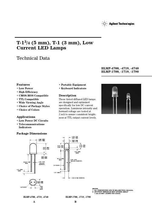
HLMP-7000, -7019, -7040Package DimensionsA BHLMP-1700, -1719, -1790HLMP-4700, -4719, -4740Note:1. θ1/2 is the typical off-axis angle at which the luminous intensity is half the axial luminous intensity.Part Numbering SystemHLMP-X7XX - X X X XXMechanical Option00: Bulk01: Tape & Reel, Crimped Leads02, BH: Tape & Reel, Straight LeadsA1, B1: Right Angle Housing, Uneven LeadsA2, B2: Right Angle Housing, Even LeadsFH: 2 Iv bins select with Inventory ControlColor Bin Options0: Full color bin distributionB: Color bins 2 & 3 onlyMaximum Iv Bin Options0: Open (No. max. limit)Others: Please refer to the Iv bin TableMinimum Iv Bin OptionsPlease refer to the Iv Bin TableColor Option00: GaP HER19: GaP Yellow40: GaP Green90: GaP GreenPackage Options4: T-13/4 (5 mm)1: T-1 (3 mm)Electrical/Optical Characteristics at T A = 25°CTest Symbol Description T-13/4T-1Min.Typ.Max.Units Conditions V F Forward Voltage47001700 1.7 2.0V 2 mA47191719 1.8 2.547401790 1.9 2.2V R Reverse Breakdown47001700 5.0V I R = 50 µA Voltage47191719 5.047401790 5.0λd Dominant47001700626nm Note 1 Wavelength4719171958547401790569∆λ1/2Spectral Line4700170040nmHalfwidth47191719364740179028τS Speed of Response4700170090ns471917199047401790500C Capacitance4700170011pF V F = 0,4719171915 f = 1 MHz4740179018RθJ-PIN Thermal47001700260[3]°C/W Junction to Resistance47191719290[4]Cathode Lead47401790λPEAK Peak Wavelength47001700635nm Measurement47191719583at peak47401790565ηV Luminous Efficacy47001700145lumens Note 247191719500watt47401790595Notes:1. The dominant wavelength, λd, is derived from the CIE chromaticity diagram and represents the single wavelength which defines thecolor of the device.2. The radiant intensity, I e, in watts per steradian, may be found from the equation I e = I V/ηV, where I V is the luminous intensity incandelas and ηV is luminous efficacy in lumens/watt.3. T-13/4.4. T-1.ParameterMaximum RatingUnits Power DissipationRed 24mW(Derate linearly from 92°C at 1.0 mA/°C)Yellow 36Green24DC and Peak Forward Current7mA Transient Forward Current (10 µs Pulse)[1]500mA Reverse Voltage (I R= 50 µA) 5.0VOperating Temperature Range Red/Yellow -55°C to 100°C Green-20°C to 100°CStorage Temperature Range -55°C to +100°C Lead Soldering Temperature 260°C for 5 seconds[1.6 mm (0.063 in.) from body]Note:1. The transient peak current is the maximum non-recurring peak current the devices can withstand without damaging the LED die and wire bonds. It is not recommended that the device be operated at peak currents beyond the Absolute Maximum Peak Forward Current.Figure 2. Forward Current vs. Forward Voltage.Figure 3. Relative Luminous Intensity vs. Forward Current.VOLTAGE – V624810Maximum tolerance for each bin limit is ±18%.Maximum tolerance for each bin limit is ±18%.Maximum tolerance for each bin limit is ±18%.Tolerance for each bin limit is ±0.5 nm.Mechanical Option MatrixMechanical Option Code Definition00Bulk Packaging, minimum increment 500 pcs/bag01Tape & Reel, crimped leads, min. increment 1300 pcs/bag for T-1 3/4, 1800pcs/bag for T-102Tape & Reel, straight leads, min. increment 1300 pcs/bag for T-1 3/4, 1800pcs/bag for T-1A1T-1, Right Angle Housing, uneven leads, minimum increment 500 pcs/bagA2T-1, Right Angle Housing, even leads, minimum increment 500 pcs/bagB1T-1 3/4, Right Angle Housing, uneven leads, minimum increment 500 pcs/bagB2T-1 3/4, Right Angle Housing, even leads, minimum increment 500 pcs/bagBH T-1, Tape & Reel, straight leads, minimum increment 2000 pcs/bagFH Devices that require inventory control and 2 I v bin selectR1Tape & Reel, crimped leads, reeled counter clockwise, cathode lead leavingthe reel firstNote:All categories are established for classification of products. Products may not be available in all categories. Please contact your local Agilent representative for further clarification/information./semiconductors For product information and a complete list of distributors, please go to our web site.For technical assistance call:Americas/Canada: +1 (800) 235-0312 or (916) 788-6763Europe: +49 (0) 6441 92460China: 10800 650 0017Hong Kong: (+65) 6756 2394India, Australia, New Zealand: (+65) 6755 1939 Japan: (+81 3) 3335-8152(Domestic/Interna-tional), or 0120-61-1280(Domestic Only) Korea: (+65) 6755 1989Singapore, Malaysia, Vietnam, Thailand, Philippines, Indonesia: (+65) 6755 2044 Taiwan: (+65) 6755 1843Data subject to change.Copyright © 2003 Agilent Technologies, Inc. September 10, 20035988-8054EN。
LME49713MANOPB系列规格书,Datasheet 资料
±0.05 0.29
±1.0
mV (max) μV/°C
PSRR
Average Input Offset Voltage Shift vs VSUPPLY = ±5V to ±15V
Power Supply Voltage
(Note 8)
100
95
dB (min)
IB
Input Bias Current
20213201
Metal Can
20213202
N = National Logo Z = Assembly plant code
X = 1 Digit date code TT = Die traceability L49713 = LME49713 MA = Package code
Order Number LME49713HA See NS Package Number H08C
132 ±1900
30
50
MHz V/μs MHz
ns
Equivalent Input Noise Voltage
fBW = 20Hz to 20kHz
en
f = 1kHz
Equivalent Input Noise Density
f = 10Hz
0.26
0.6
μVRMS
(max)
1.9
4.0
nV/√Hz
RSOURCE = 10Ω, fIN = 1kHz, and TJ = 25°C, unless otherwise specified.
Symbol
Parameter
Conditions
LME49713
Typical
Limit
ASP-134603-01;中文规格书,Datasheet资料

A
REVISION H
01
2.835 72.00 REF
5
40
.945 24.00 REF (TYP)
PROPRIETARY NOTE
THIS DOCUMENT CONTAINS INFORMATION CONFIDENTIAL AND PROPRIETARY TO SAMTEC, INC. AND SHALL NOT BE REPRODUCED OR TRANSFERRED TO OTHER DOCUMENTS OR DISCLOSED TO OTHERS OR USED FOR ANY PURPOSE OTHER THAN THAT WHICH IT WAS OBTAINED WITHOUT THE EXPRESSED WRITTEN CONSENT OF SAMTEC, INC.
.2500 6.350
.1500 3.810
.521 13.23
(ALL DIMENSIONS SYMMETRIC ABOUT THE CENTERLINE)
PROPRIETARY NOTE
THIS DOCUMENT CONTAINS INFORMATION CONFIDENTIAL AND PROPRIETARY TO SAMTEC, INC. AND SHALL NOT BE REPRODUCED OR TRANSFERRED TO OTHER DOCUMENTS OR DISCLOSED TO OTHERS OR USED FOR ANY PURPOSE OTHER THAN THAT WHICH IT WAS OBTAINED WITHOUT THE EXPRESSED WRITTEN CONSENT OF SAMTEC, INC.
QCT417.3-2001-车用电线束插接器第3部分单线片式插接件的尺寸和特殊要求

QCT417.3-2001-车用电线束插接器第3部分单线片式插接件的尺寸和特殊要求QC/T417.1~417.5-2001(2001-08-21发布,2001-12-01实施)前言本标准参照ISO 8092.1~.4系列标准制定。
本标准在车用电线束插接器的总标题下分为五部分:——第1部分:定义,试验方法和一般性能要求(汽车部分)——第2部分:试验方法和一般性能要求(摩托车部分)——第3部分:单线片式插接件尺寸和特殊要求——第4部分:多线片式插接件尺寸和特殊要求——第5部分:用于单线和多线插接的圆柱式插接件尺寸和特殊要求随着我国汽车产品技术水平的不断提高,对电器插接器的要求越来越高,因此,在参照ISO8092.2:1996制定车用电线束插接器试验方法和性能要求标准过程中,汽车整车厂普遍认为ISO 8092中对插接器性能要求较低,希望提高性能要求,而这些提高的性能要求,对于摩托车用插接器显得过高,因此,经协商将插接器试验方法和一般性能要求分汽车和摩托车两部分制定,即第1部分:定义,试验方法和一般性能要求(汽车部分),在采用ISO 8092.2:1996内容基础上,将部分性能要求提高并相应增加了一些性能要求及相应的试验方法,试验方法除有些直接采用国际标准的内容,其余均采用国家标准及相关行业标准。
第2部分:试验方法和一般性能要求(摩托车部分),技术内容等同采用ISO 8092.1996。
QC/T 417.3~QC/T 417.5分别等同采用ISO 8092.1、.3、.4:1996的内容。
本系列标准自实施之日起同时代替QC/T 417-1999,QC/T 418-1999,QCn 29012-1991。
本系列标准由国家机械工业局提出。
本系列标准由全国汽车标准化技术委员会归口。
本系列标准第1部分起草单位:鹤壁天海汽车电气有限公司;主要起草人:王来生、王荣喜。
本系列标准第2部分起草单位:高邮电器厂;主要起草人:何玉光、吴长红、曹俊。
- 1、下载文档前请自行甄别文档内容的完整性,平台不提供额外的编辑、内容补充、找答案等附加服务。
- 2、"仅部分预览"的文档,不可在线预览部分如存在完整性等问题,可反馈申请退款(可完整预览的文档不适用该条件!)。
- 3、如文档侵犯您的权益,请联系客服反馈,我们会尽快为您处理(人工客服工作时间:9:00-18:30)。
Options
Features
Panel Connectivity
Reliability
Interface:TMDS panel interface
Function Controls:External buttons,
Functions: Inverter brightness, power on/off Indicators: LED 1 - input signal present, LED 2 - backlight status
Dimensions:107mm x 92mm (4.2” x 3.6”)Form Factor: DV standard & mounting holes Inverter Support:DPMS Enable Inverter Voltage:24V DC Panel Signal: TMDS
Panel Voltage:18V DC (derived on-board)
Power Requirements:24V DC, 1.5W (controller only)Status Indicator:Dual Color LED support.
2560x1600 WQXGA Samsung LTB300M1-P01 Samsung LTM300M1-P01 LG LM300W01-A3TFT:
Calculated Mean Time Between Failures - In excess of
100,000 hours. Warranty - 3 years
Copyright Digital View 2009
Custom Engineering Services - Custom input timing, panel timing, splash screen, OSD Menu, conformal coatings, layouts etc.
Custom layouts & connectors. Alternative panel support.
Input:
Dual Channel DVI-D
DVI-2560
The Digital View DVI-2560 interface controller for ultra high resoution WQXGA LCD panels.
The DVI-2560 is a purpose built high-performance dual-channel DVI interface controller capable of driving 2560x1600
WQXGA LCD panels from Samsung and LG. Operating from a single 24 volt power supply, the controller derives all necessary voltages for the controller, panel and inverter operation.
Accessories
416940020-3Audio Amplifier
416040010-3Inverter Interface board
Kit 60110-3OSD Button Board
Kit 60121-3OSD Membrane Kit
Kit 60125-3OSD Membrane Kit
Instruction Manual *See accessories page on website for details.
Available Documentation
Digital View Ltd.
16th Floor Millennium City 3 370 Kwun Tong Road
Kwun Tong, Hong Kong
Tel: (852) 2861-3615
Fax: (852) 2520-2987
Email: hksales@ Digital View Inc.
18440 T echnology Drive
Morgan Hill, CA 95037
USA
Tel: 1 (408) 782-7773
Fax: 1 (408) 782-7883
Email: ussales@
Digital View Ltd.
6 Marylebone Passage,
London, W1W 8EX
UK
Tel: +44 20-7631-2150
Fax: +44 20-7436-1299
Email: uksales@
ASIA USA EUROPE Please visit our web site for more information: 。