TD1509
泰德半导体

No.Type Vi Vo Fre Package Ioηmax OCPOTPSP技术误差同类PIN对PIN产品型号适用产品范围备注1TD1410 3.6~20 1.222~18380KHz SOP-82A95%Y≤3%MPS1410/9141/ACT4060/ATC4012/FSP3126/ZA3020等便携式DVD、LCD显示驱动板。
液晶显示器、液晶电视、数码相框.电信ADSL.车载DVD/VCD/CD.GPS。
安防等TD1410采用CMOS工艺/6寸晶圆。
是一款高效率低损耗,工作稳定,性价比很高使用面广的DC/DC电源管理芯片。
3TD15341~200.8~18380KHz SOP82A95%Y≤2%MP1513 TD1513路由器,便携式DVD、机顶盒、平板电脑、笔记本电脑、LCD显示驱动板.液晶显示器、液晶电视、数码相框.电信ADSL Modem.车载DVD/VCD/CD.GPS安防等。
TD1534采用CMOS工艺/8寸晶圆。
是一款高效率低损耗,工作电压范围大,工作稳定/性价比很高,使用面广的DC/DC电源管理芯片。
5TD1583 3.6~28 1.222~26380KHz SOP-83A95%Y≤3%MP1583LCD显示驱动板。
液晶显示器、液晶电视、数码相框.电信ADSLModemL.车载DVD/VCD/CD.GPS。
安防等产品。
TD1583采用CMOS工艺/6寸晶圆。
是一款高效率低损耗,工作电压范围大,工作稳定/性价比很高,使用面广的DC/DC电源管理芯片。
6TD1591 3.6V-32V 1.222~30380KHz SOP-82A95%Y≤3%MP1591LCD液晶显示器、LCD液晶电视、数码相框.电信ADSL ModemL.车载DVD/VCD/CD.GPS。
TD1591采用CMOS工艺/6寸晶圆。
是一款高效率低损耗,工作电压范围大,工作稳定/性价比很高,使用面广的DC/DC电源管理芯片。
GC1509中文资料
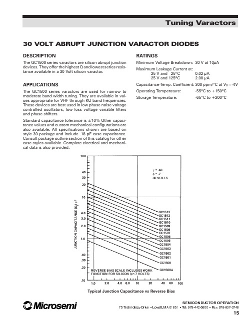
30VOLT ABRUPT JUNCTION VARACTOR DIODESDESCRIPTIONThe GC1500series varactors are silicon abrupt junction devices.They offer the highest Q and lowest series resis-tance available in a 30Volt silicon varactor.APPLICATIONSThe GC1500series varactors are used for narrow tomoderate band width tuning.They are available in val-ues appropriate for VHF through KU band frequencies.These devices are best used in low phase noise voltage controlled oscillators,low loss voltage variable filters and phase shifters.Standard capacitance tolerance is ±10%Other capaci-tance values and custom mechanical configurations are also available.All specifications shown are based on style 30package and include .18pF case capacitance.Consult package outline section of this catalog for other case styles plete electrical and mechani-cal data is alsoprovided.RATINGSMinimum Voltage Breakdown:30V at 10µA Maximum Leakage Current at:25V and 25ºC 0.02µA 25V and 125ºC 2.00µACapacitance-Temp.Coefficient:300ppm/ºC at V R =-4V Operating Temperature:-55ºC to +150ºC Storage Temperature:-65ºC to +200ºCTuning Varactors30VOLT ABRUPT JUNCTION VARACTOR DIODESELECTRICAL SPECIFICATIONS:T A =25°CNOTES:1.When ordering,specify the desired case style by adding its number as a suffix to the model number.Some limitations apply -consult factory for details.2.These values include a package capacitance of .18P ..3.Q is calculated from:Q=1π5jwhere f=50MHz and R I =Series resistance measured a 1GHz using transmission loss techniques.Capacitance is measured at 1MHz.4.GC1500A only available in Die Form.SEMICONDUCTOR OPERATION75T echnology Drive Lowell,MA 01851 T el:978-442-5600 Fax:978-937-374816Tuning Varactors。
xl1509中文资料_数据手册_参数

万联芯城-电子元器件采购网,提供一站式配套, 解决物料烦恼,万联芯城为长电,顺络,先科ST等国内知名原厂的 授权代理商,所售电子元器件均为原厂原装正品,万联芯城BOM 报价流程:联系商城客服-提交物料清单-等待报价-下单-商城发货, 万联芯城现货库存销售能够满足多种客户的物料需求,一站式报价 为客户节省采购成本,点击进入万联芯城。
9070T150D1产品数据表说明书

9070T150D1Industrial Control TransformersProduct Description PRODUCT DESCRIPTIONControl power transformers from Schneider Electric set the industry standard for design innovation and performance. They are designed with low impedance windings for excellent voltage regulation, and can accomodate the high inrush current associated with contactors, starters, solenoids, and relays.A variety of designs are available to meet the diverse needs of panel builders and machinery OEMs. The versatility of our control transformer line offers unparalleled options for design engineers. We also have one of the most extensive offering of custom products with no minimum order requirements.We have a national network of distributors to ensure prompt delivery, including industry leading delivery on custom products. In most cases, we can design, manufacture, and ship a custom unit in two weeks or less.The Global Product Offering—Type TType T is our most popular and complete line of control transformers. It comes with unmatched design innovations for top performance and is manufactured using the most advanced insulating materials. The Type T control transformer is the best choice if size and cost are of concern.The Exceptional Regulation Offering —Type EOConstructed with traditional materials and manufacturing processes, Type EO transformers are UL and CSA Component Recognized. Units are designed for 55°C rise. All units are 60HZ rated, withde-rated VA levels for 50HZ.Transformers with Fuse Block Protection—Types TF and EOFWe offer both product lines with factory installed overcurrent protection fuse blocks.Type TF and EOF transformers consist of two primary fuse blocks and one secondary fuse block, a configuration that meets the majority of overcurrent needs by panel builders and machinery OEMs. Since the fuse blocks are pre-wired and mounted on top of the transformer, the Type TF and EOF transformers have the same footprint as the Type T and Type EO units, respectively. This design frees up space normally used for separate fuse blocksWe also have an extensive fuse block offering for custom applications. See the overcurrent section of this catalog for full details.Leaded Control Transformer LineSchneider Electric offers transformers with internally pre-wired 24-inch primary and secondary leads, instead of terminal boards, to make installation easier and faster for many applications. These are only available for single voltage primary and single voltage secondary applications.MultiTapSchneider Electric offers Type T and Type EO transformers in the MultiTap version. The MultiTap control transformer was designed to respond to the increased need for voltage and stock flexibility. It combines multiple primary voltages with one or more secondary voltages, all in a single transfomer. The most flexible MultiTap voltage is the Universal, available on the Type T product line only. It allows for standard primary voltages of 208 to 600V and 110, 115, or 120V secondary voltages.Industrial Control TransformersType T TransformersTYPE T TRANSFORMERSThe Type T units are designed for the global market and are the best choice when size and cost are of concern. This is our most popular and complete offering of industrial control transformers. The following features are included:•50/60 Hz rated•Customer installed accessories (Finger-Safe covers, fuse blocks, fuse clips)•Type T transformers are designed with various temperature classes:—25–150 VA with a 55° C temperature rise, 105° C insulation —200–350 VA with a 80° C temperature rise, 130° C insulation —500–5000 VA with a 115° C temperature rise, 180° C insulationSchneider Electric manufactures a wide variety of voltage combinations for control transformers. The voltage combinations are expressed as “Voltage Codes”, and are embedded within the catalog number of the transformer. Standard codes are listed. If the voltage combination you need is not listed, please call your Schneider Electric distributor for assistance.CE MarkingIndustrial control transformers (ICTs) entering the European Union (EU) after January 1, 1997 are required by EU standards to have CE marking or Declaration of Conformity to CE. EU documentation requires compliance with specification EN 61 558 of the Low Voltage Directive. Type T ICTs from Schneider Electric comply with this specification and are third party tested to T ÜV standards, which adhere to, and are accepted by, EU standards. A Declaration of Conformity for all Type T units is available upon request.Because of different overload criteria in the CE specification,Schneider Elecric dual rates these transformers for UL VA, cUL VA, CSA VA, NOM VA and CE VA ratings (see “Type T VA Ratings” table). Because they are widely used with control circuit panels, ICTs are also required to comply with EN 60 204 and EN 61 558 in these applications. The Type T transformer line complies with EN 60 204 when Fingersafe ® covers are installed.For more information regarding CE marking, please contact your local Schneider Electric field sales office.Type T VA RatingsUL, cUL, CSA and NOM VA RatingCEVA Rating252550507575100100150150200200250160300200350250500300750500100063015001000200015003000200050003000Type T ListingsListingFileVA RangeUL E61239, Guide XPTQ225–5000cUL E612391500–5000CSALR37055, Guide 184-N-9025–1000EN947923, EN 61 558/01.89 (TUV ref: 00941-RAG/sg E9371495E01)25–2009579078, EN 61 558/01.89 (TUV ref: 00941-RAG/sg E9471921E01)250–10009579078, EN 61 558/01.89 (TUV ref: 00941-RAG/sg E9471921.02E01)1500–3000Industrial Control TransformersType T Transformers120 Volt Control SecondaryVoltage and Connection OptionsVoltage CodeVoltagesConnectionsPrimary SecondaryPrimarySecondaryD1220 x 440230 x 460240 x 480110115120220/230/240 V:Connect to H1 and H4Jumper H1 with H3Jumper H2 with H4440/460/480 V:Connect to H1 and H4Jumper H2 with H3Connect to X1 and X2DimensionsVA CatalogNumberFigureAcc. KeyA BCEFSlotsULCEINmmINmmINmmINmmINmmINmm25259070T25D11I 3.0979 3.0076 2.5866 2.0051 2.50640.20 x 0.38 5 x 1050509070T50D11I 3.0979 3.0076 2.5866 2.0051 2.50640.20 x 0.38 5 x 1075759070T75D11I 3.3485 3.3886 2.8973 2.3861 2.81710.20 x 0.48 5 x 121001009070T100D11I 3.3485 3.3886 2.8973 2.3861 2.81710.20 x 0.48 5 x 121501509070T150D11I 3.5991 3.7595 3.2081 2.8873 3.13800.20 x 0.38 5 x 102002009070T200D11I 3.5991 3.7595 3.2081 2.8873 3.13800.20 x 0.38 5 x 102501609070T250D12I 5.30135 3.7595 3.2182 2.8873 3.13800.20 x 0.38 5 x 103002009070T300D12I 4.74120 4.50114 3.8498 2.5665 3.75950.20 x 0.38 5 x 103502509070T350D12I 5.11130 4.50114 3.8498 3.0076 3.75950.20 x 0.38 5 x 105003009070T500D12I 5.49139 4.50114 3.8498 3.5690 3.75950.20 x 0.38 5 x 107505009070T750D12I 5.61143 5.25133 4.51115 3.4387 4.381110.28 x 0.567 x 1410006309070T1000D12I 6.30160 5.25133 4.51115 4.31109 4.381110.28 x 0.567 x 14150010009070T1500D12I 5.921507.06179 6.17157 4.13105 5.811480.28 x 0.567 x 14200015009070T2000D12I 7.171827.06179 6.17157 4.56116 5.811480.28 x 0.567 x 14300020009070T3000D13I 7.241849.002298.75222 4.631187.631940.44 x 1.1311 x 29500030009070T5000D13I9.152329.002298.752226.561677.631940.44 x 1.1311 x 2914T R A N S F O R M E R SIndustrial ControlClass 9070 / Refer to Catalogs 9070CT9901, 7400CT9601Square D ® Type T and MultiTap™ TransformersType T transformers are designed with low impedance windings forexcellent voltage regulation and can accommodate the high inrush current associated with contactors, starters, solenoids, and relays. As the most popular and complete line of control transformers with unmatched design innovations for top performance, Type Ts are manufactured using the most advanced insulating materials and are the best choice if size and cost are of concern. It is available in the MultiTap version, designed to respond to the increased need for voltage and stock flexibility. It combines multiple primary voltages with one or more secondary voltages, all in a single transformer.VAVA Catalog No.$ PriceH W D W e i g h t (l b s )U L /C S A /N O MCEin (mm)in (mm)in (mm)Primary 240 x 480 Secondary 120; Primary 230 x 460 Secondary 115; or Primary 220 x 440Secondary 11025259070T25D174.00 2.58 (65.5) 3.00 (76.2) 3.09 (78.5) 2.550509070T50D177.00 2.58 (65.5) 3.00 (76.2) 3.09 (78.5) 2.575759070T75D192.00 2.89 (73.4) 3.38 (85.8) 3.34 (84.8) 3.81001009070T100D1103.00 2.89 (73.4) 3.38 (85.8) 3.34 (84.8) 3.81501509070T150D1110.00 3.20 (81.3) 3.75 (95.3) 3.59 (91.2) 5.52002009070T200D1136.00 3.20 (81.3) 3.75 (95.3) 3.59 (91.2) 5.52501609070T250D1159.00 3.25 (82.6) 3.75 (95.3) 5.25 (133.4)7.130********T300D1176.00 3.80 (96.5) 4.50 (114.3) 4.70 (119.4)8.53502509070T350D1187.00 3.80 (96.5) 4.50 (114.3) 5.09 (129.3)10.55003009070T500D1233.00 3.80 (96.5) 4.50 (114.3) 5.46 (138.7)11.97505009070T750D1322.00 4.43 (112.5) 5.25 (133.4) 5.66 (143.8)11.010*********T1000D1390.00 4.43 (112.5) 5.25 (133.4) 6.04 (153.4)20.6150010009070T1500D1558.00 6.16 (156.5)7.06 (179.3) 5.81 (147.6)34.0200015009070T2000D1678.00 6.16 (156.5)7.06 (179.3)7.04 (178.8)47.0300020009070T3000D1941.008.46 (214.9)9.00 (228.6) 6.86 (174.2)60.0500030009070T5000D11582.008.46 (214.9)9.00 (228.6)8.73 (221.7)89.0Primary 208 Secondary 12050509070T50D390.00 2.58 (65.5) 3.00 (76.2) 3.09 (78.5) 2.575759070T75D3108.00 2.89 (73.4) 3.38 (85.8) 3.34 (84.8) 3.81001009070T100D3121.00 2.89 (73.4) 3.38 (85.8) 3.34 (84.8) 3.81501509070T150D3153.00 3.20 (81.3) 3.75 (95.3) 3.59 (91.2) 5.52002009070T200D3195.00 3.20 (81.3) 3.75 (95.3) 3.59 (91.2) 5.52501609070T250D3242.00 3.25 (82.6) 3.75 (95.3) 5.25 (133.4)7.130********T300D3248.00 3.80 (96.5) 4.50 (114.3) 4.70 (119.4)8.53502509070T350D3288.00 3.80 (96.5) 4.50 (114.3) 5.09 (129.3)10.55003009070T500D3314.00 3.80 (96.5) 4.50 (114.3) 5.46 (138.7)11.97505009070T750D3443.00 4.43 (112.5) 5.25 (133.4) 5.66 (143.8)11.010*********T1000D3558.00 4.43 (112.5) 5.25 (133.4) 6.04 (153.4)20.6150010009070T1500D3780.00 6.16 (156.5)7.06 (179.3) 5.81 (147.6)34.0200015009070T2000D3905.00 6.16 (156.5)7.06 (179.3)7.04 (178.8)47.0300020009070T3000D31276.008.46 (214.9)9.00 (228.6) 6.86 (174.2)60.0500030009070T5000D32010.008.46 (214.9)9.00 (228.6)8.73 (221.7)89.0Primary 600 Secondary 120; Primary 575 Secondary 115; or Primary 550 Secondary 11050509070T50D590.00 2.58 (65.5) 3 (76.2) 3.09 (78.5) 2.575759070T75D5108.00 2.89 (73.4) 3.38 (85.8) 3.34 (84.8) 3.81001009070T100D5121.00 2.89 (73.4) 3.38 (85.8) 3.34 (84.8) 3.81501509070T150D5153.00 3.20 (81.3) 3.75 (95.3) 3.59 (91.2) 5.52002009070T200D5195.00 3.20 (81.3) 3.75 (95.3) 3.59 (91.2) 5.52501609070T250D5242.00 3.25 (82.6) 3.75 (95.3) 5.25 (133.4)7.130********T300D5248.00 3.80 (96.5) 4.50 (114.3) 4.70 (119.4)8.53502509070T350D5288.00 3.80 (96.5) 4.50 (114.3) 5.09 (129.3)10.55003009070T500D5314.00 3.80 (96.5) 4.50 (114.3) 5.46 (138.7)11.97505009070T750D5443.00 4.43 (112.5) 5.25 (133.4) 5.66 (143.8)11.010*********T1000D5558.00 4.43 (112.5) 5.25 (133.4) 6.04 (153.4)20.6150010009070T1500D5780.00 6.16 (156.5)7.06 (179.3) 5.81 (147.6)34.0200015009070T2000D5905.00 6.16 (156.5)7.06 (179.3)7.04 (178.8)47.0300020009070T3000D51276.008.46 (214.9)9.00 (228.6) 6.86 (174.2)60.0500030009070T5000D52010.008.46 (214.9)9.00 (228.6)8.73 (221.7)89.0Primary 120 Secondary 120; Primary 115 Secondary 115; or Primary 110 Secondary 11050509070T50D24312.00 2.58 (65.5) 3.00 (76.2) 3.09 (78.5) 2.575759070T75D24324.00 2.89 (73.4) 3.38 (85.8) 3.34 (84.8) 3.81001009070T100D24326.00 2.89 (73.4) 3.38 (85.8) 3.34 (84.8) 3.81501509070T150D24348.00 3.20 (81.3) 3.75 (95.3) 3.59 (91.2) 5.52002009070T200D24475.00 3.20 (81.3) 3.75 (95.3) 3.59 (91.2) 5.52501609070T250D24477.00 3.25 (82.6) 3.75 (95.3) 5.25 (133.4)7.130********T300D24481.00 3.8 (96.5) 4.50 (114.3) 4.70 (119.4)8.53502509070T350D24483.00 3.80 (96.5) 4.50 (114.3) 5.09 (129.3)10.55003009070T500D24498.00 3.80 (96.5) 4.50 (114.3) 5.46 (138.7)11.97505009070T750D24560.00 4.43 (112.5) 5.25 (133.4) 5.66 (143.8)11.010*********T1000D24594.00 4.43 (112.5) 5.25 (133.4) 6.04 (153.4)20.6150010009070T1500D24717.00 6.16 (156.5)7.06 (179.3) 5.81 (147.6)34.0200015009070T2000D24929.00 6.16 (156.5)7.06 (179.3)7.04 (178.8)47.0300020009070T3000D241463.008.46 (214.9)9.00 (228.6) 6.86 (174.2)60.0500030009070T5000D242010.008.46 (214.9)9.00 (228.6)8.73 (221.7)89.0Primary 277 Secondary 120Primary 277 Secondary 120 (continued)2002009070T200D4195.00 3.20 (81.3) 3.75 (95.3) 3.59 (91.2) 5.52501609070T250D4242.00 3.25 (82.6) 3.75 (95.3) 5.25 (133.4)7.130********T300D4248.00 3.80 (96.5) 4.50 (114.3) 4.70 (119.4)8.53502509070T350D4288.00 3.80 (96.5) 4.50 (114.3) 5.09 (129.3)10.55003009070T500D4314.00 3.80 (96.5) 4.50 (114.3) 5.46 (138.7)11.97505009070T750D4443.00 4.43 (112.5) 5.25 (133.4) 5.66 (143.8)11.010*********T1000D4558.00 4.43 (112.5) 5.25 (133.4) 6.04 (153.4)20.6150010009070T1500D4780.00 6.16 (156.5)7.06 (179.3) 5.81 (147.6)34.0200015009070T2000D4905.00 6.16 (156.5)7.06 (179.3)7.04 (178.8)47.0300020009070T3000D41276.008.46 (214.9)9.00 (228.6) 6.86 (174.2)60.0500030009070T5000D42010.008.46 (214.9)9.00 (228.6)8.73 (221.7)89.0VA VA Catalog No.$ PriceHW D W e i g h t (l b s )U L /C S A /N O MCEin (mm)in (mmin (mm)Primary 240 x 480 Secondary 120/240; Primary 230 x 460 Secondary 115/230; orPrimary 220 x 440 Secondary 110/22050509070T50D31125.00 2.58 (65.5) 3.00 (76.2) 3.09 (78.5) 2.575759070T75D31131.00 2.89 (73.4) 3.38 (85.8) 3.34 (84.8) 3.81001009070T100D31138.00 2.89 (73.4) 3.38 (85.8) 3.34 (84.8) 3.81501509070T150D31182.00 3.20 (81.3) 3.75 (95.3) 3.59 (91.2) 5.52002009070T200D31235.00 3.20 (81.3) 3.75 (95.3) 3.59 (91.2) 5.52501609070T250D31248.00 3.25 (82.6) 3.75 (95.3) 5.25 (133.4)7.130********T300D31290.00 3.80 (96.5) 4.50 (114.3) 4.70 (119.4)8.53502509070T350D31303.00 3.80 (96.5) 4.50 (114.3) 5.09 (129.3)10.55003009070T500D31339.00 3.80 (96.5) 4.50 (114.3) 5.46 (138.7)11.97505009070T750D31473.00 4.43 (112.5) 5.25 (133.4) 5.66 (143.8)11.010*********T1000D31558.00 4.43 (112.5) 5.25 (133.4) 6.04 (153.4)20.6150010009070T1500D31816.00 6.16 (156.5)7.06 (179.3) 5.81 (147.6)34.0200015009070T2000D31905.00 6.16 (156.5)7.06 (179.3)7.04 (178.8)47.0300020009070T3000D311486.008.46 (214.9)9.00 (228.6) 6.86 (174.2)60.0500030009070T5000D312010.008.46 (214.9)9.00 (228.6)8.73 (221.7)89.0Primary 120 x240 Secondary 120/240; Primary 115 x 230 Secondary 115/230; orPrimary 110 x 2200 Secondary 110/22050509070T50D55312.00 2.58 (65.5) 3.00 (76.2) 3.09 (78.5) 2.575759070T75D55324.00 2.89 (73.4) 3.38 (85.8) 3.34 (84.8) 3.81001009070T100D55326.00 2.89 (73.4) 3.38 (85.8) 3.34 (84.8) 3.81501509070T150D55348.00 3.20 (81.3) 3.75 (95.3) 3.59 (91.2) 5.52002009070T200D55475.00 3.20 (81.3) 3.75 (95.3) 3.59 (91.2) 5.52501609070T250D55477.00 3.25 (82.6) 3.75 (95.3) 5.25 (133.4)7.130********T300D55481.00 3.80 (96.5) 4.50 (114.3) 4.70 (119.4)8.53502509070T350D55483.00 3.80 (96.5) 4.50(114.3) 5.09 (129.3)10.55003009070T500D55498.00 3.80 (96.5) 4.50 (114.3) 5.46 (138.7)11.97505009070T750D55560.00 4.43 (112.5) 5.25 (133.4) 5.66 (143.8)11.010*********T1000D55594.00 4.43 (112.5) 5.25 (133.4) 6.04 (153.4)20.6150010009070T1500D55856.00 6.16 (156.5)7.06 (179.3) 5.81 (147.6)34.0200015009070T2000D55929.00 6.16 (156.5)7.06 (179.3)7.04 (178.8)47.0300020009070T3000D551588.008.46 (214.9)9.00 (228.6) 6.86 (174.2)60.0500030009070T5000D552010.008.46 (214.9)9.00 (228.6)8.73 (221.7)89.0Primary 240 X 480 Secondary 24/120 (24 V limited to 20% Capacity)50509070T50D1590.00 2.58 (65.5) 3.00 (76.2) 3.09 (78.5) 2.575759070T75D15108.00 2.89 (73.4) 3.38 (85.8) 3.34 (84.8) 3.81001009070T100D15138.00 2.89 (73.4) 3.38 (85.8) 3.34 (84.8) 3.81501509070T150D15153.00 3.20 (81.3) 3.75 (95.3) 3.59 (91.2) 5.52002009070T200D15195.00 3.2 0(81.3) 3.75 (95.3) 3.59 (91.2) 5.52501609070T250D15248.00 3.25 (82.6) 3.75 (95.3) 5.25 (133.4)7.130********T300D15290.00 3.80 (96.5) 4.50 9114.3) 4.70 (119.4)8.53502509070T350D15303.00 3.80 (96.5) 4.50 (114.3) 5.09 (129.3)10.55003009070T500D15339.00 3.80 (96.5) 4.50 (114.3) 5.46 (138.7)11.97505009070T750D15473.00 4.43 (112.5) 5.25 (133.4) 5.66 (143.8)11.010*********T1000D15558.00 4.43 (112.5) 5.25 (133.4) 6.04 (153.4)20.6150010009070T1500D15816.00 6.16 (156.5)7.06 (179.3) 5.81 (147.6)34.0200015009070T2000D15905.00 6.16 (156.5)7.06 (179.3)7.04 (178.8)47.0300020009070T3000D151486.008.46 (214.9)9.00 (228.6) 6.86 (174.2)60.0500030009070T5000D152010.008.46 (214.9)9.00 (228.6)8.73 (221.7)89.0Primary 480 Secondary 24050509070T50D1290.00 2.58 (65.5) 3.00 (76.2) 3.09 (78.5) 2.575759070T75D12324.00 2.89 (73.4) 3.38 (85.8) 3.34 (84.8) 3.81001009070T100D12121.00 2.89 (73.4) 3.38 (85.8) 3.34 (84.8) 3.81501509070T150D12153.00 3.20 (81.3) 3.75 (95.3) 3.59 (91.2) 5.52002009070T200D12195.00 3.20 (81.3) 3.75 (95.3) 3.59 (91.20) 5.52501609070T250D12242.00 3.25 (82.6) 3.75 (95.3) 5.25 (133.4)7.130********T300D12248.00 3.80 (96.5) 4.50 (114.3) 4.70 (119.4)8.53502509070T350D12288.00 3.80 (96.5) 4.50 (114.3) 5.09 (129.3)10.55003009070T500D12314.00 3.80 (96.5) 4.50 (114.3) 5.46 (138.7)11.97505009070T750D12443.00 4.43 (112.5) 5.25 (133.4) 5.66 (143.8)11.010*********T1000D12558.00 4.43 (112.5) 5.25 (133.4) 6.04 (153.4)20.6150010009070T1500D12780.00 6.16 (156.5)7.06 (179.3) 5.81 (147.6)34.0200015009070T2000D12905.00 6.16 (156.5)7.06 (179.3)7.04 (178.8)47.0VA VA Catalog No.$ PriceH W DW e i g h t (l b s )U L /C S A /N O MCEin (mm)in (mm)in (mm)9070T150D1。
GNSS定位原理
7.基站墩标1套,型号:SOLD-DB-180
8.基站地面机柜1台,型号:SOLD-JDG-500
9.天线罩1个,型号:SOLD-DQL-ATQ-1
流动站子系统
1.卫星接收机5套,型号:SOLD-DQL-RTK-01
2.卫星接收天线(含天线罩)10套,型号:SOLD-DQL-OT-1
3.电源5套,型号:MWDR-75-24
GNSS定位系统是采用在堆场合适位置建立基准站,在堆取料机的回转中心和悬臂中部或者头部中心点安装GPS流动站,通过GPS的位置信息和空间几何算法,得出两台堆取料机之间的最小距离。它是武汉索尔德新开发的一项专利产品,有效避免了堆取料机发生碰撞的可能性。本系统可以实时计算出堆取料机悬臂的相对位置和距离,实现多台堆取料机在同一个场垛中安全作业,大幅提高安全作业效率。它所包含的设备包括:
4.交换机5套,型号:SOLD-JKJ-02
5.基站地面机柜5套,型号:SOLD-LCG-300
地面控制室通讯系统
1.嵌入式控制器1套,型号:SOLD-DQL-CT
2.交换机1台,型号:SOLD-JKJ-02
3.协议转换模块1个,型号:SOLD-EthernetIP
4.嵌入式控制器软件1套,型号:SOLD-DQL-CT-SOFT-02
参考站系统
1.卫星接收机1套,型号:SOLD-DQL-RTK-01
2.卫星接收天线1套,型号:SOLD-DQL-OT-1
3.防雷保护系统1套,型号:SOLD-DVK220
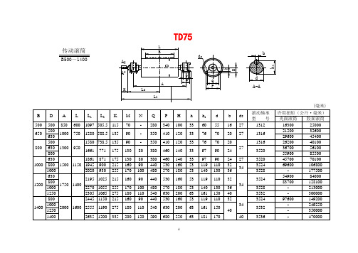
TD75、DTⅡ及DTⅡ(A)型滚筒
501
TD3A35
503
1000
630
TD4A14
442
TD4A24
467
TD4A34
471
800
TD4A15
682
TD4A25
715
TD4A35
719
1000
—
—
TD4A26
963
TD4A36
969
1250
630
TD5A14
660
TD5A24
691
TD5A34
696
800
TD5A15
759
33
76
70
20
27
1316
21200
32600
630
29600
45400
800
500
1300
950
1580
738.5
135
90
-
350
410
120
33
76
70
20
27
1316
26200
40100
630
1661
771
175
130
80
380
460
140
33
97
90
24
3520
36700
56100
800
1784
1400
—
—
TD6A28
2203
TD6A38
2216
说明:
1.滚筒为钢板焊接结构,分光面、胶面两种。
胶面又分铸胶和包胶两种。
TD1A13≈TD1A1.3≈ TD1A13
2.滚筒直径D在1000毫米以上者只有胶面滚
xl1509中文资料

特点:宽输入电压范围4.5v-40v,输出可调范围1.23v-37v,最大占空比100%,最小饱和压降1.5V,150kHz固定开关频率,恒定的2A电流输出能力,内部优化的功率晶体管设计,高效率,出色的线性输出和负载可调,TTL关闭功能,内置频率补偿,热关断功能,xl1509是一个150kHz固定频率脉冲宽度调制(降压)DC / DC转换器。
它具有2A的负载驱动能力,高效率,低纹波和出色的线性度。
它具有良好的负载调节能力,只需要最少的外部组件。
可调输出易于使用,内置频率补偿和固定频率振荡器。
PWM控制电路可将占空比从0调整到100%。
具有使能功能,内置的过流和短路保护功能,在过流和短路保护的情况下,xl1509的工作频率将从150kHz降低到50KHz。
内置频率补偿模块最大程度地减少了xl1509的外部组件。
图1. Xl1509封装类型初步数据表2A 150kHz 40V Buck DC-DC转换器xl1509 Rev 2.0 Xinlong Semiconductor Limited Corporation 2引脚设置图2. Xl1509引脚结构(顶视图)表1引脚说明引脚编号引脚名称1 VIN电压输入引脚,xl1509在4.5V至40V的DC电压下工作,输入外部连接适用于对地的大旁路电容,以消除输入噪声。
2 SW电源开关输出引脚(SW)。
输出是提供电源输出的开关节点。
5〜8 GND接地引脚,必须仔细设计。
该引脚必须放置在硝基基极二极管的外部,并将输出电容器接地,以防止由感应电压引起的开关电流毛刺输入到xl1509。
3 FB的反馈引脚(FB),通过外部电阻分裂环路,反馈是检测并调节输出电压,反馈端电压为1.23V。
开/关使能引脚。
如果驱动器的开/关引脚为低电平,则设备将被打开;否则,设备将被打开。
如果引脚为高电平,则设备将关闭。
4. Xl1509典型应用电路12v-5v / 2A初步数据表2A 150kHz 40V Buck DC-DC转换器xl1509 Rev 2.0新龙半导体有限公司订购信息组件编号标记标识封装温度范围无铅封装类型xl1509-adje1 xl1509-adje1管xl1509- 3.3e1 xl1509-3.3e1管xl1509-5.0e1 xl1509-5.0e1管xl1509-12e1 xl1509-adjtre1 xl1509-adjtre1碳带和卷轴xl1509-3.3tre1 xl1509-3.3tre1碳带和卷轴xl1509-5.0tre1 xl1509-5.0tree1碳带和卷轴xl1509-12tre1 xl1509-12tre1碳带和卷轴soic-8-40oC〜85oc xl1513e1 xl1513e1碳带和卷轴xlsemi无铅产品符合ROHS标准初步数据表2A 150kHz 40V降压DC-DC转换器xl1509 Rev 2.0新龙半导体有限公司5最大额定值(注1)参数符号值单位输入电压Vin-0.3至45 V反馈引脚电压VFB-0.3至VIN V开/关引脚电压von / off-0.3至VIN V输出开关引脚电压voutput-0.3至VIN V功耗PD内部极限MW热阻(soic8)(结温,无热量,自然通风)RJA 100 ﹣0 ﹣2C / W PN结工作温度TJ-40至125 ﹣0 ﹣2C储存温度Tstg-铅(PIN)耐焊接温度(热焊接,10秒)引线260.0.2c ESD(人体模型)2000 V注1:超过所列的最大额定值会导致设备永久损坏。
AP1509-50SG-13原版数据手册.pdf-EasyDatasheet

DescriptionThe AP1509 series are monolithic IC designed for a step-down DC/DC converter, and own the ability of driving a 2A load without additional transistor. It saves board space. The external shutdown function can be controlled by logic level and then come into standby mode. The internal compensation makes feedback control having good line and load regulation without external design. Regarding protected function, thermal shutdown is to prevent over temperature operating from damage, and current limit is against over current operating of the output switch. If current limit function occurs and V FB is down below 0.5V, the switching frequency will be reduced. The AP1509 series operates at a switching frequency of 150KHz thus allow smaller sized filter components than what would be needed with lower frequency switching regulators. Other features include a guaranteed +4% tolerance on output voltage under specified input voltage and output load conditions, and +15% on the oscillator frequency. The output version included fixed 3.3V, 5V, 12V, and an adjustable type. The chips are available in a standard 8-lead SOP-8 package. Pin Assignments(Top View)V INGND FBGND OutputGNDGND SDSOP-8LFeatures• Output Voltage: 3.3V, 5V, 12V and Adjustable Output Version• Adjustable Version Output Voltage Range, 1.23V to 18V+4%• 150KHz +15% Fixed Switching Frequency• Voltage Mode Non-Synchronous PWM Control• Thermal-Shutdown and Current-Limit Protection• ON/OFF Shutdown Control Input• Operating Voltage can be up to 22V• Output Load Current: 2A• SOP-8L Packages• Low Power Standby Mode• Built-in Switching Transistor On Chip• SOP-8L: Available in “Green” Molding Compound (No Br, Sb)• Lead Free Finish/ RoHS Compliant (Note 1) Applications• Simple High-Efficiency Step-Down Regulator • On-Card Switching Regulators• Positive to Negative ConverterNotes: 1. EU Directive 2002/95/EC (RoHS). All applicable RoHS exemptions applied. Please visit our website atTypical Application Circuit(1) Fixed Type Circuit(2) Adjustable Type CircuitV OUT = V FB ×(1 +R2R1)V FB = 1.23V R2 = 1K ~ 3K(3) Delay Start CircuitPin DescriptionsFunctional Block DiagramGNDOutput V INSDFBPin NameDescriptionV INOperating voltage inputOutput Switching output GND Ground FB Output voltage feedback control SDON/OFF ShutdownAbsolute Maximum RatingsSymbol Parameter Rating UnitESD HBM Human Body Model ESD Protection 2 KVESD MM Machine Model ESD Protection 200 V V IN SupplyVoltage +24 V V SD ON/OFF Pin Input Voltage -0.3 to +18 VV FB Feedback Pin Voltage -0.3 to +18 VV OUT Output Voltage to Ground -1 VP D Power Dissipation Internally Limited WT ST Storage Temperature -65 to +150 o CT J Operating Junction Temperature -40 to +125 o C Recommended Operating ConditionsSymbol Parameter Min Max UnitI OUT OutputCurrent 0 2 AVoltage 4.5 22 V V OP OperatingT A Operating Ambient Temperature -20 85 o CElectrical CharacteristicsUnless otherwise specified, V IN = 12V for 3.3V, 5V, adjustable version and V IN = 18V for the 12V version. I LOAD = 0.5A Specifications with boldface type are for full operating temperature range, the other type are for T J = 25ºC.Symbol Parameter Conditions Min Typ. Max UnitI FB Feedback Bias Current V FB = 1.3V(Adjustable version only)-10-50nA-100F OSC OscillatorFrequency 127 150 173KHz 110 173F SCP Oscillator Frequency ofShort Circuit ProtectWhen current limit occurredand V FB < 0.5V, T a = 25 o C10 30 50 KHzV SAT SaturationVoltage I OUT = 2ANo outside circuitV FB = 0V force driver on1.251.4V1.5DC Max. Duty Cycle (ON) V FB = 0V force driver on 100% Min. Duty Cycle (OFF) V FB = 12V force driver off 0I CL CurrentLimit Peak currentNo outside circuitV FB = 0V force driver on3 AI L Output = 0OutputLeakageCurrentNo outside circuitV FB = 12V force driver off-200uA Output = -1 V IN =22V -5 mAI Q QuiescentCurrent V FB = 12V force driver off 5 10 mAI STBY Standby QuiescentCurrentON/OFF pin = 5VV IN = 22V70150uA200V ILON/OFF Pin Logic InputThreshold Voltage Low (regulator ON) -1.30.6VV IH High (regulator OFF) 2.0 -I H ON/OFF Pin Logic InputCurrentV LOGIC = 2.5V (OFF) -0.01uAI L ON/OFF Pin Input Current V LOGIC = 0.5V (ON) -0.1 -1θJA ThermalResistance SOP-8L Junction tocase15 o C/WθJC Thermal Resistancewith a copper area ofapproximately 3 in2SOP-8LJunction toambient70 o C/WElectrical Characteristics (Continued)Typical Performance CharacteristicsAP1509 Efficiency vs. Temperature(V IN =12V, V OUT =5V, Io=2A)AP1509 Efficiency vs. Temperature(V IN =12V, V OUT=3.3V, Io=2A)AP1509 Saturation Voltage vs. Temperature(V IN =12V, V FB=0V, VSD=0)AP1509 Switch Current Limit vs. Temperature(V IN =12V, V FB=0V)AP1509 Supply Current vs. Temperature(V IN =12V, No Load, Von/off =0V(Switch ON) ,Von/off =5V(Switch OFF))Typical Performance Characteristics (Continued)AP1509 Threshold Voltage vs. Temperature(V IN =12V, Io=100mA)AP1509 ON/OFF Current vs. ON/OFF Voltage(V IN=12V)AP1509 Frequency vs. Temperature (V IN =12V, Io=500mA, V OUT=5V)AP1509 Feedback Current vs. Temperature(V IN =12V, V OUT=5V, Vfb=1.3V)AP1509 Output Voltage vs. Temperature(V IN =12V, Io=2A)Typical Performance Characteristics (Continued)Header Frequency vs. Temperature Feedback Voltage vs. Temperature(V IN=15V, V OUT=5V)Supply Current vs. Temperature (V IN=15V, V OUT=5V, l OUT=0A) Supply Current vs. Supply Voltage (V IN=15V, V OUT=5V, l OUT=0A)Efficiency vs. Output Current(V IN=15V, V OUT=5V)Efficiency vs. Output Current(V IN=15V, V OUT=3.3V)Functions DescriptionPin Functions+V INThis is the positive input supply for the IC switching regulator. A suitable input bypass capacitor must be presented at this pin to minimize voltage transients and to supply the switching currents needed by the regulator.GroundCircuit ground.OutputInternal switch. The voltage at this pin switches between (+V IN – V SAT) and approximately – 0.5V, with a duty cycle of approximately V OUT / V IN. To minimize coupling to sensitive circuitry, the PC board copper area connected to this pin should be minimized.FeedbackSenses the regulated output voltage to complete the feedback loop.SDAllows the switching regulator circuit to be shutdown using logic level signals thus dropping the total input supply current to approximately 150uA. Pulling this pin below a threshold voltage of approximately 1.3V turns the regulator on, and pulling this pin above 1.3V (up to a maximum of 18V) shuts the regulator down. If this shutdown feature is not needed, the SD pin can be wired to the ground pin.Thermal ConsiderationsThe SOP-8L package needs a heat sink under most conditions. The size of the heat sink depends on the input voltage, the output voltage, the load current and the ambient temperature. The AP1509 junction temperature rises above ambient temperature for a 2A load and different input and output voltages. The data for these curves was taken with the AP1509 (SOP-8L package) operating as a buck-switching regulator in an ambient temperature of 25o C (still air). These temperature increments are all approximate and are affected by many factors. Higher ambient temperatures require more heat sinker.For the best thermal performance, wide copper traces and generous amounts of printed circuit board copper should be used in the board layout (One exception is the output (switch) pin, which should not have large areas of copper). Large areas of copper provide the best transfer of heat (lower thermal resistance) to the surrounding air, and moving air lowers the thermal resistance even further.Package thermal resistance and junction temperature increments are all approximate. The increments are affected by a lot of factors. Some of these factors include board size, shape, thickness, position, location, and even board temperature. Other factors are, trace width, total printed circuit copper area, copper thickness, single or double-sided, multi-layer board and the amount of solder on the board.The effectiveness of the PC board to dissipate heat also depends on the size, quantity and spacing of other components on the board, as well as whether the surrounding air is still or moving. Furthermore, some of these components such as the catch diode will add heat to the PC board and the heat can vary as the input voltage changes. For the inductor, depending on the physical size, type of core material and the DC resistance, it could either act as a heat sink taking heat away from the board, or it could add heat to the board.AP1509Document number: DS31016 Rev. 4 - 211 of 13June 2010© Diodes IncorporatedOrdering InformationS : SOP-8L13 : Tape & ReelBlank : Adjustable33 : 3.3V 50 : 5.0V 12 : 12VL : Lead Free G : GreenDevicePackageCode Packaging (Note 2) 13” Tape and ReelQuantity Part Number Suffix AP1509-XXSL-13S SOP-8L 2500/Tape & Reel -13 AP1509-XXSG-13SSOP-8L2500/Tape & Reel -13Notes: 2. Pad layout as shown on Diodes Inc. suggested pad layout document AP02001, which can be found on our website at /datasheets/ap02001.pdf.Marking Information(1) SOP-8L( Top View )1509-XXLogoPart No.AP1509Document number: DS31016 Rev. 4 - 212 of 13June 2010© Diodes IncorporatedPackage Outline Dimensions (All Dimensions in mm)(1) Package Type: SOP-8LDetail "A"(Unit: mm)AP1509Document number: DS31016 Rev. 4 - 213 of 13June 2010© Diodes Incorporated。
XL1509 DEMO board 说明书
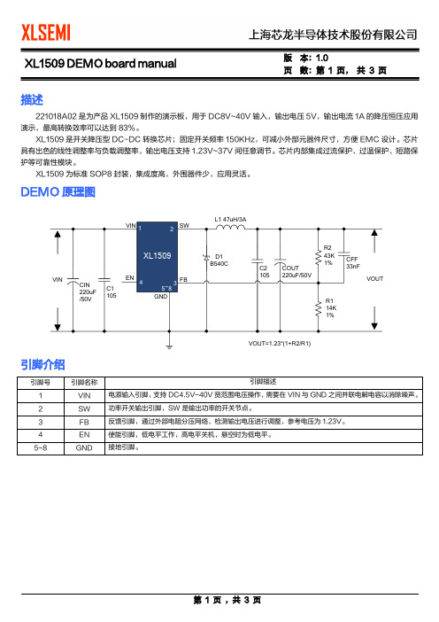
页数:第1 页,共3 页描述221018A02是为产品XL1509制作的演示板,用于DC8V~40V输入,输出电压5V,输出电流1A的降压恒压应用演示,最高转换效率可以达到83%。
XL1509是开关降压型DC-DC转换芯片;固定开关频率150KHz,可减小外部元器件尺寸,方便EMC设计。
芯片具有出色的线性调整率与负载调整率,输出电压支持1.23V~37V间任意调节。
芯片内部集成过流保护、过温保护、短路保护等可靠性模块。
XL1509为标准SOP8封装,集成度高,外围器件少,应用灵活。
DEMO原理图引脚介绍页 数:第 2 页, 共 3 页物料清单序号 数量 参考位号 说明生产商型号 生产商 1 2 C1,C2 1uF,50V,Ceramic,X7R,0805 C2012X7R1H105K TDK 2 1 CFF 33nF,50V,Ceramic,X7R,0603 C1608X7R1H333K TDK 3 2 CIN, COUT220uF,50V,Electrolytic,(10*16) YXJ-50V-220uFRubycon 4 1 D1 40V,5A,SMC,Schottky Barrier RectifierB540CDIODES5 1 L1 47uH,3A,(12*6.5)6 1 R1 14K Ω,1%,1/16W,Thick Film,0603 RC0603FR-0714KL Yageo7 1 R2 43K Ω,1%,1/16W,Thick Film,0603 RC0603FR-0743KLYageo 8 1U140V,2A,BUCK,DC-DC Converter,SOP8XL1509XLSEMIDEMO 实物图PCB 布局35mm顶层 底层25mm页数:第3 页,共3 页应用信息输入电容选择在连续模式中,转换器的输入电流是一组占空比约为VOUT/VIN的方波。
为了防止大的瞬态电压,必须采用针对最大RMS电流要求而选择低ESR(等效串联电阻)输入电容器。
XL1509 中文datasheet
特点:宽输入电压范围 4.5V-40V 输出可调范围1.23V-37V最大占空比100%最小饱和压降1.5V150KHz固定开关频率恒定2A电流输出能力内部优化功率管设计高效率极好的线性输出且负载可调 TTL关断能力内建频率补偿,热关断功能,限流功能,短路保护功能可选封装形式:SOP-8应用领域:LCD监控器与LCD电视数码像框机顶盒调制解调器通信/网络设备概述XL1509是一个150KHz固定频率脉宽调制(降压型)DC/DC转换器。
具有2A 负载驱动能力并且效率高,低纹波和极好的线性,负载调节能力好,仅需最少外部元件。
可调输出使用简单,内建频率补偿和固定频率震荡器。
脉宽调制控制电路可以线性调节占空比从0到100%。
具有使能功能,内置过流和短路保护功能,当发生过流和短路保护时,XL1509工作频率将从150KHz降到50KHz。
内置频率补偿模块使XL1509外部元件最少。
图1.XL1509封装类型2. XL1509引脚结构(顶视图)电压输入引脚,XL1509工作在直流电压的旁路电容到地来消除输入噪声。
功能模块图3: XL1509功能块方框图典型应用电路图4.XL1509典型应用电路12V-5V/2A元件号码记号标识温度范围无铅无铅XL1509-ADJE1 XL1509-ADJE1XL1509-3.3E1 XL1509-3.3E1XL1509-5.0E1 XL1509-5.0E1XL1509-12E1 XL1509-12E1大电流走线要粗,短,不拐弯图5:XL1509测试电路和版图指导的电阻。
12V~3.3V/2A典型应用电路图6 XL1509系统参数测试电路(12V~3.3V/2A) 12V~5V/2A典型应用电路图7 XL1513系统参数测试电路(12V~5V/2A) ADJ版本典型应用电路Preliminary Datasheet 2A 150KHz 40V Buck DC to DC Converter XL1509Rev 2.0 XinLong Semiconductor Limited Corporation11 封装信息SOP8封装机械尺寸SOIC-8单位:毫米(英寸)。
XL1509
ŋ
XL1509-12 Electrical Characteristics
Ta = 25℃;unless otherwise specified. Symbol Parameter Test Condition Min. Typ. Max. Unit
Figure1. Package Type of XL1509
Rev 2.0 1
XLSEMI
2A 150KHz 40V Buck DC to DC Converter Pin Configurations
Datasheet XL1509
VIN OUTPUT FEEDBACK ON/OFF
1 2 XL1509 3 4
8 7 6 5
GND GND GND GND
Figure2. Pin Configuration of XL1509 (Top View) Table 1 Pin Description Pin Number 1 2 5~8 Description Supply Voltage Input Pin. XL1509 operates from a 4.5V to VIN 40V DC voltage. Bypass Vin to GND with a suitably large capacitor to eliminate noise on the input. Power Switch Output Pin (SW). Output is the switch node that OUTPUT supplies power to the output. Ground Pin. Care must be taken in layout. This pin should be placed outside of the Schottky Diode to output capacitor GND ground path to prevent switching current spikes from inducing voltage noise into XL1509. Feedback Pin (FB). Through an external resistor divider FEEDBACK network, Feedback senses the output voltage and regulates it. The feedback threshold voltage is 1.23V. Enable Pin. Drive ON/OFF pin low to turn on the device, drive ON/OFF it high to turn it off. Floating is default low. Pin Name
器具操作手册-1509
器具操作手册测试地址::8006/OA_HTML/RF.jsp?function_id=28910用户名:TEST0101 密码:12345供应商用户名:SA900132401 密码:12345一、器具维护员操作二、器具管理员操作三、供应商操作一、器具维护员操作:包括器具类别维护和器具设置1、器具类别维护:按归属组进行器具类别维护,归属组需系统管理员配置;2、器具维护:维护器具编码、名称等信息,如下图,其中单个租金、计时类型、免费时长用于计算租金的。
二、器具管理员操作,包括:器具接收、回收、租借、归还、盘点、现有量查询、交易查询1、接收,供应商按送货单号打印器具单的,输入送货单号、条码号、供应商编码都可以查询出对应器具单,输入正确的仓库和数量,保存即可。
2、回收,新建回收单,输入供应商编码、仓库等信息;其中“转MES厂确认”勾选表示该单会到MES系统中(后同)。
保存确定,系统即扣减库存。
如果确定后发现错误,做“废弃”即可,系统会反向做帐冲掉原来数据。
3、器具租借:1)用于与供应商之间的租借,类型为借出、借入,分别表示供应商从美的租借和美的从供应商租借2)如果维护了租金,则会根据预计归还日期与租借日期之差并减掉免费时长,再乘以单个租金,进行计算预计应付租金;3)如果是借出,该信息会反馈到供应商门户,由供应商确认收到。
如果供应商确认则行状态为“供应商已收”。
4、器具归还:1)类型为借出归还、借入归还;分别表示供应商把器具归还美的、美的归还供应商器具;2)用获取行的形式,从原来已租借的数据中获取;对原来租借的数量可以分多次归还;3)如果维护了租金,则会根据归还日期与租借日期之差并减掉免费时长,再乘以单个租金,进行计算实际应付租金;4)如果是借入归还,该信息会反馈到供应商门户,由供应商确认收到。
5、子库存转移:1)分为发料和收料两步执行,发料制单,收料确认进行账务处理;打印功能双方都可以;2)类型分为内部和供应商,如果是供应商,会记录是哪个供应商的器具进行了子库存转移,系统处理账务时会对该供应商器具做相应的子库存转移处理。
山西省矿山工程专业期刊参考目录

煤炭科学研究总院北京开采研究所
10
煤炭工程
11-4658/TD
11
煤炭加工与综合 利用
11-2627/TD
12
煤质技术
11-3862/TD
煤炭工业规划设计研究院 中国煤炭加工利用协会 煤炭科学研究总院北京煤化学所
13
建井技术
11-2456/TD
煤科总院北京建井研究所
14
矿产勘查
11-5875/TD
有色金属矿产地质调查中心
28
重庆理工大学学 报(自然科学版)
50-1053/T
29
电子科技大学学 报
51-1207/T
30
四川大学学报(工 程科学版)
51-1596/T
主办单位
浙江大学 浙江工业大学
南昌大学 山东大学 郑州大学 武汉大学 武汉工业学院 湖北工业大学 湖南工业大学 华南理工大学 广东工业大学 广西工学院 重庆理工大学 电子科技大学 四川大学
97
浙江大学学报 (工学版)
33-1245/T
浙江大学
98 矿业研究与开发 43-1215/TD
中国有色金属学会; 长沙矿山研究院
99
矿冶工程
43-1104/TD
长沙矿冶研究院;中国金属学会
100
采矿技术
43-1347/TD
长沙矿山研究院
101 矿业工程研究 43-1493/TD
湖南科技大学
111
机械设计
中煤科工集团;常州自动化研究院
150
自动化与信息工 程
44-1632/TP
广东省科学院自动化工程研制中心;广州自动化 学会
151
淮海工学院学报 (自然科学版)
td1850说明书
td1850说明书产品概述TD1850 是一款宽量限、多量值、高精度的交直流标准源仪器,可精准输出交流电压 / 电流,直流电压 / 电流,准确度为 0.05 级,兼具电阻模拟和脉冲输出功能,是校准万用表及其他交直流电测仪表的理想仪器。
参考标准:JJG 124-2005《电流表、电压表、功率表及电阻表检定规程》、JJF 1587-2016《数字多用表校准规范》、JJF 1284-2011《交直流电表校验仪校准规范》( 同电测控【天恒测控前身】参与起草 ) 等。
功能特点交直流电量输出:电压最大达 1100 V,电流最大达 22 A 或 33 A ,F:DC,45 Hz ~ 1100 Hz。
直流电阻模拟:10 Ω~220 MΩ,连续可调;脉冲输出频率范围:1 Hz ~ 2 MHz。
量值输出模式:具有标准源和调节输出源二种模式,方便数字表和模拟表的检定。
量值调节方式:具有“定点输出、电位器调节、旋转编码器、步进调节”等多种方式。
输出开关按键:通过一键操作可任意关闭或接通当前输出通道。
负载能力优异:在满负荷条件下确保量值稳定准确,可覆盖电动系指针式表的检定。
人机功能良好:大屏液晶显示,采用触摸加数字按键的操作模式,方便用户手动检表。
钳形表校准 ( 选件 ):可配接 50 T 的线圈,最大产生 1100 At 的等效电流,用于校准钳形表。
变送器检测 ( 选件 ):具有交直流变送器的二次直流信号测量的功能。
专用软件 ( 选件 ):支持被检表的全自动或全自动校准,数据管理和证书导出。
主要应用检定或校准 0.2 级及以下的交流电压表、电流表,直流电压表、电流表检定或校准 0.2 级及以下的多用表、万用表,0.5 级及以下的电阻表校准钳形表 ( 选件 )、校准交直流变送器 ( 选件 ) 功能特点电量输出:电压最大达 1100 V,电流最大达 22 A 或 33 A ,F:DC,45 Hz ~ 1100Hz。
电阻模拟:10 Ω~ 220 MΩ,连续可调;脉冲输出频率范围:1 Hz ~ 2 MHz。
暗装镀锌接地测试盒规格型号表
暗装镀锌接地测试盒规格型号表
摘要:
1.暗装镀锌接地测试盒的简介
2.暗装镀锌接地测试盒的规格
3.暗装镀锌接地测试盒的型号
4.暗装镀锌接地测试盒的应用领域
正文:
一、暗装镀锌接地测试盒的简介
暗装镀锌接地测试盒是一种用于测试接地系统的设备,主要功能是检测接地系统的电阻值,以确保接地系统的可靠性和安全性。
它广泛应用于电力、电信、铁路、石油化工、军工等领域。
二、暗装镀锌接地测试盒的规格
暗装镀锌接地测试盒的规格主要根据其容量来划分,常见的规格有50A、100A、200A、300A 等。
其中,容量越大,测试的范围和精度就越高。
三、暗装镀锌接地测试盒的型号
暗装镀锌接地测试盒的型号主要根据其功能和性能来划分,常见的型号有DZG-100A、DZG-200A、DZG-300A 等。
其中,型号的字母和数字代表了测试盒的特性和参数。
四、暗装镀锌接地测试盒的应用领域
暗装镀锌接地测试盒广泛应用于各种接地系统中,包括电力系统的接地、电信系统的接地、铁路系统的接地、石油化工系统的接地、军工系统的接地
等。
TD、JH9系列 说明书
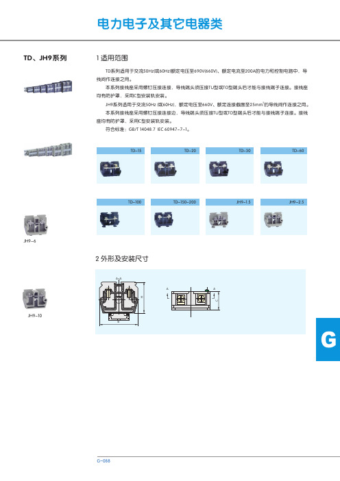
、TD JH9系列TD系列适用于交流50Hz(或60Hz)额定电压至、额定电流至200A的电力和控制电路中,导线间作连接之用。
本系列接线座采用螺钉压接连接,导线端头须压接TU型或TO型端头后才能与接线端子连接。
接线座均有防护罩,采用C型安装轨安装。
2JH9系列适用于交流50Hz (或60Hz),额定电压至660V、额定连接截面至25mm的导线间作连接之用。
本系列接线座采用螺钉压接连接边,导线端头须压接TU型或TO型端头后才能与接线端子连接。
接线座均有防护罩,采用C型安装轨安装。
符合标准:GB/T 14048.7 IEC 60947-7-1。
690V(660V)TD-60JH9-2.5TD-30JH9-1.5TD-20TD-150-200TD-15TD-1001 适用范围JH9-6G JH9-102 外形及安装尺寸C C C C C C C C C C C C C C C C C C C C C C CTD-15A JH9-1.5G TD-15AG JH9-2.5AG TD-20A JH9-2.5G TD-20AG JH9-6TD-30A JH9-6G TD-30AG JH9-10TD-60A JH9-10ZG TD-60AG JH9-25TD-100A JH9-25ZG TD-100AG TD-150/1TD-150/10TD-200/1TD-200/1030.230.230.2393939394343434352.352.352.352.3505060606868686882212.5124414.514.55518.318.37.37.322225527.832027.832020.221.521.5292930.530.5333334.534.542.242.24444404041.541.55157515723456789101112131415161718192021222324JH9-253.1 订货时应注明产品的型号、接线面积或电流、类别、数量。
- 1、下载文档前请自行甄别文档内容的完整性,平台不提供额外的编辑、内容补充、找答案等附加服务。
- 2、"仅部分预览"的文档,不可在线预览部分如存在完整性等问题,可反馈申请退款(可完整预览的文档不适用该条件!)。
- 3、如文档侵犯您的权益,请联系客服反馈,我们会尽快为您处理(人工客服工作时间:9:00-18:30)。
General DescriptionThe TD1509 is a series of easy to use fixed and adjustable step-down (buck) switch-mode voltage regulators. These devices are available in fixed output voltage of 5V,3.3V an adjustable output version. Both versions are capable of driving a 2A load with excellent line and load regulation. Requiring a minimum number of external components, these regulators are simple to use and include internal frequency compensation, and a fixed-frequency oscillator. The output voltage is guaranteed to ±3% tolerance under specified input voltage and output load conditions. Theoscillator frequency is guaranteed to ±15%. External shutdown is included, featuring typically 80 µA standby current. Self protection features include a two stagefrequency reducing current limit for the output switch andan over temperature shutdown for complete protectionunder fault conditions.The TD1509 is available in SOP8 and DIP8 packages.Featuresz 5V,3.3V and adjustable output versions z Output adjustable from 1.23v to 43Vz Fixed 150KHz frequency internal oscillator z Guaranteed 3A output load current zInput voltage range up to 45V z Low power standby mode, I Q typically 80 µA z TTL shutdown capabilityz Excellent line and load regulation z Requires only 4 external components z High efficiency z Thermal shutdown and current limit protection z Available in SOP8 and DIP8 packages Applications z Simple High-efficiency step-down regulatorz On-card switching regulatorsz Positive to negative converterz LCD monitor and LCD TVz DVD recorder and PDP TVz Battery chargerz Step-down to 3.3V for microprocessorsPackage TypesFigure 1. Package Types of TD1509Pin ConfigurationsDIP8/SOP8Figure 2 Pin Configuration of TD1509 (Top View)Pin DescriptionPin Number Pin Name Description1 Vin Input supply voltage2 Output Switching output 5~8 GND Ground3 FB Output voltage feedback4 ON/OFFON/OFF shutdownActive is “Low” or floatingOrdering InformationTD1509 □ □Circuit Type Output Voltage:3:3.3V5:5VPackage R:ADJP: SOP8D: DIP8Function BlockFigure 3 Function Block Diagram of TD1509Absolute Maximum RatingsNote1: Stresses greater than those listed under Maximum Ratings may cause permanent damage to the device. This is a stress rating only and functional operation of the deviceat these or any other conditions above those indicated in the operation is not implied. Exposure to absolute maximum rating conditions for extended periods may affectreliability.UnitValueParameter SymbolInput Voltage V IN-0.3 to 45 VFeedback Pin Voltage V FB-0.3 to Vin+0.3 VON/OFF Pin Voltage V EN-0.3 to Vin+0.3 VOutput Pin Voltage V SW-0.3 to Vin+0.3 VmWlimitedPower Dissipation P D InternallyºCOperating Junction Temperature T J 150Storage Temperature T STG-65 to 150 ºCLead Temperature (Soldering, 10 sec) T LEAD 260 ºCESD (HBM) 2000 VLevel3 MSLThermal Resistance-Junction to Ambient RθJA 85 ºC / WThermal Resistance-Junction to Case RθJC 45 ºC / WRecommended Operating ConditionsParameter Symbol Min. Max. UnitInput Voltage V IN 3.6 45 VºCOperating Junction Temperature T J -40 125ºCOperating Ambient Temperature T A -40 85Electrical CharacteristicsSpecifications with boldface type are for full operationg temperature range, the other type are for T J =25O C. Note1: Thermal resistance with copper area of approximately 3 in 2.Parameters Symbol Test Condition Min. Typ. Max. UnitFeedback bias current I b Adjustable only, V FB =1.3V10 50/100nAQuiescent current I QV FB =12V force driver off5 10 mAStandby quiescent current I STBY ON/OFF =5V, V IN =36V 80 200/250uAOscillator frequency F OSC127 150 173 KHzSaturation voltage V SAT I OUT =3A 1.2 1.4/1.5V Current LimitI CL Peak Current (V FB =0V)3.84.2 AOutput leakage current I LI L Output=0V (V FB =12V) 50 uA Output leakage current Output=-1V (V IN =36V) 2 30 mA ON/OFF pin logic inputThreshold voltageV IL V IH Low (Regulator ON)1.30.6VON/OFF pin input currentI H I L High (Regulator OFF) 2.0 1.3 VV LOGIC =2.5V(Regulator OFF)5 15 uAV LOGIC =0.5V(Regulator ON)0.02 5 uAThermal ResistanceJunction to Case θJC45 O C/WThermal Resistance Junction to Ambient (Note1)θJA85 OC/WElectrical Characteristics(Cont.)Specifications with boldface type are for full operationg temperature range, the other type are for T J=25O C.Note1: Thermal resistance with copper area of approximately 3 in2.Parameters SymbolTestConditionMin.Typ.Max.UnitTD1509 ADJ Vout: OutputVoltage11V≤V IN≤45V,0.2A≤I LOAD≤3A, V OUTfor 9V1.193/1.1801.231.267/1.280Vη: EfficiencyV IN=12V,V OUT=9V,I LOAD=3A88 %TD1509 5V Vout: OutputVoltage7V≤V IN≤45V,0.2A≤I LOAD≤3A4.800/4.7505.05.200/5.250Vη: Efficiency V IN=12V, I LOAD=3A 83 %TD1509 3.3V Vout: OutputVoltage4.75V≤V IN≤45V,0.2A≤I LOAD≤2A3.168/3.1353.33.432/3.465Vη: Efficiency V IN=12V, I LOAD=2A 76 %Typical Performance CharacteristicsFigure 4. Output Voltage vs. Temperature Figure 5. Switching Frequency vs. TemperatureFigure 6. Output Saturation CharacteristicsFigure 7. Quiescent Current vs. TemperatureTypical Performance Characteristics(Cont.)Figure 8. ON/OFF Pin Voltage Figure 9. ON/OFF Pin Sink CurrentFigure 10. Output Saturation CharacteristicsTypical Application CircuitFigure 11. Typical Application of TD1509 For 3.3V 5VInput Voltage Inductor (L1)Output Capacitor (Cout)Through Hole Electrolytic Surface Mount Tantalum6V ~ 18V 47uh 470uf/25V 330uf/6.3V 6V ~ 45V 68uh 560uf/25V 330uf/6.3VTable 1. TD1509 Series Buck Regulator Design Procedure For 3.3VInput Voltage Inductor (L1)Output Capacitor (Cout)Through Hole Electrolytic Surface Mount Tantalum8V ~ 18V 33uh 330uf/25V 220uf/10V 8V ~ 45V 47uh 470uf/25V 330uf/10VTable 2. TD1509 Series Buck Regulator Design Procedure For 5VFigure 12. Typical Application of TD1509 For ADJNote:In PCB layout. Reserved an area for CFFVout R1 R2 Cf (Operational) 3.3V 1.6K 2.7K 33nf5V 3.6K 11K 10nf9V 6.8K 43K 1.5nf12V 1.5K 13K 1nfTable 3. Vout VS. R1, R2, Cf Select TableOutput VoltageInputVoltageInductor (L1)Output Capacitor (Cout)Through Hole Electrolytic3.3V 6V ~ 18V 47uh 470uf/25V6V ~36V 68uh 560uf/25V5V 8V ~ 18V 33uh 330uf/25V 8V ~36V 47uh 470uf/25V9V 12V~18V 47uh 330uf/25V 12V ~36V 47uh 470uf/25V12V 15V ~ 18V 47uh 220uf/25V 15V ~36V 47uh 330uf/25VTable 4. Typical Application Buck Regulator Design ProcedureFunction DescriptionPin Functions+V INThis is the positive input supply for the IC switching regulator. A suitable input bypass capacitor must be present at this pin to minimize voltage transients and to supply the switching currents needed by the regulator GroundCircuit ground.OutputInternal switch. The voltage at this pin switches between (+V IN – V SAT) and approximately – 0.5V, with a duty cycle of approximately V OUT / V IN. To minimize coupling to sensitive circuitry, the PC board copper area connected to this pin should be kept a minimum. FeedbackSenses the regulated output voltage to complete the feedback loop.ON/OFFAllows the switching regulator circuit to be shutdown using logic level signals thus dropping the total input supply current to approximately 80uA. Pulling this pin below a threshold voltage of approximately 1.3V turns the regulator on, and pulling this pin above 1.3V (up to a maximum of 25V) shuts the regulator down. If this shutdown feature is not needed, the ON /OFF pin can be wired to the ground pin or it can be left open, in either case the regulator will be in the ON condition.Thermal ConsiderationsThe TD1509 is available in two packages,. The TD1509 junction temperature rises above ambient temperature for a 2A load and different input and output voltages. The data for these curves was taken with the TD1509 operating as a buck switching regulator in an ambient temperature of 25o C (still air). These temperature rise numbers are all approximate and there are many factors that can affect these temperatures. Higher ambient temperatures require more heat sinking. The SOP8/DIP8 surface mount package tab is designed to be soldered to the copper on a printed circuit board. The copper and the board are the heat sink for this package and the other heat producing components, such as the catch diode and inductor. The PC board copper area that the package is soldered to should be at least 0.4 in2, and ideally should have 2 or more square inches of 2 oz. Additional copper area improves the thermal characteristics, but with copper areas greater than approximately 6 in2, only small improvements in heat dissipation are realized. If further thermal improvements are needed, double sided, multilayer PC board with large copper areas and/or airflow are recommended.The TD1509 junction temperature rise above ambient temperature with a 2A load for various input and output voltages. This data was taken with the circuit operating as a buck switching regulator with all components mounted on a PC board to simulate the junction temperature under actual operating conditions. This curve can be used for a quick check for the approximate junction temperature for various conditions, but be aware that there are many factors that can affect the junction temperature. When load currents higher than 2A are used, double sided or multilayer PC boards with large copper areas and/or airflow might be needed, especially for high ambient temperatures and high output voltages. For the best thermal performance, wide copper traces and generous amounts of printed circuit board copper should be used in the board layout. (Once exception toFunction Description(Cont.)this is the output (switch) pin, which should not have large areas of copper.) Large areas of copper provide the best transfer of heat (lower thermal resistance) to the surrounding air, and moving air lowers the thermal resistance even further.Setting the Output VoltageThe output voltage is set using a resistive voltage divider from the output voltage to FB(TD1509-ADJ) The voltage divider divides the output voltage down by the ratio:VFB = VOUT * R1 / (R1 + R2)Thus the output voltage is:VOUT = 1.235 * (R1 + R2) / R1R1 can be as high as 100KΩ, but a typical value is 10KΩ. Using that value, R2 is determined by:R2 ~= 8.18 * (VOUT – 1.235) (KΩ)For example, for a 3.3V output voltage, R1 is 10KΩ, and R2is 17KΩ.InductorThe inductor is required to supply constant current to the output load while being driven by the switched input voltage. A larger value inductor results in less ripple current that in turn results in lower output ripple voltage. However, the larger value inductor has a larger physical size, higher series resistance, and/or lower saturation current. Choose an inductor that does not saturate under the worst-case load conditions. A good rule for determining the inductance is to allow the peak-to-peak ripple current in the inductor to be approximately 30% of the maximum load current. Also, make sure that the peak inductor current (the load current plus half the peak to peak inductor ripple current) is below the TBDA minimum current limit. The inductance value can be calculated by the equation: L = (VOUT) * (VIN-VOUT) / VIN * f * ∆IWhere VOUT is the output voltage, VIN is the input voltage, f is the switching frequency, and ∆I is thepeak-to-peak inductor ripple current.Input CapacitorThe input current to the step-down converter is discontinuous, and so a capacitor is required to supply the AC current to the step-down converter while maintaining the DC input voltage. A low ESR capacitor is required to keep the noise at the IC to a minimum. Ceramic capacitors are preferred, but tantalum orlow-ESR electrolytic capacitors may also suffice.The input capacitor value should be greater than 10μF. The capacitor can be electrolytic, tantalum or ceramic. However since it absorbs the input switching current it requires an adequate ripple current rating. Its RMS current rating should be greater than approximately1/2 of the DC load current.For insuring stable operation should be placed as close to the IC as possible. Alternately a smaller high quality ceramic 0.1μF capacitor may be placed closer to the IC and a larger capacitor placed further away. If using this technique, it is recommended that the larger capacitor be a tantalum or electrolytic type. All ceramic capacitors should be places close to the TD1509.Output CapacitorThe output capacitor is required to maintain the DC output voltage. Low ESR capacitors are preferred to keep the output voltage ripple low. The characteristics of the output capacitor also affect the stability of the regulation control system. Ceramic, tantalum, or low ESR electrolytic capacitors are recommended. In the case of ceramic capacitors, the impedance at the switching frequency is dominated by the capacitance,Function Description(Cont.)and so the output voltage ripple is mostly independent of the ESR. The output voltage ripple is estimated to be:VRIPPLE ~= 1.4 * VIN * (fLC/fSW)^2Where VRIPPLE is the output ripple voltage, VIN is the input voltage, fLC is the resonantfrequency of the LC filter, fSW is the switching frequency. In the case of tanatalum or low- ESR electrolytic capacitors, the ESRdominates the impedance at the switching frequency, and so the output ripple is calculated as:VRIPPLE ~= ∆I * RESRWhere VRIPPLE is the output voltage ripple, ∆I is the inductor ripple current, and RESR is the equivalent series resistance of the output capacitors.Output Rectifier DiodeThe output rectifier diode supplies the current to the inductor when the high-side switch is off. To reduce losses due to the diode forward voltage and recovery times, use a Schottky rectifier.Table 1 provides the Schottky rectifier part numbers based on the maximum input voltage and current rating.Choose a rectifier who’s maximum reverse voltage rating is greater than the maximum input voltage, and who’scurrent rating is greater than the maximum load current. Feedforward Capacitor (CFF) For output voltages greater than approximately 8V, anadditional capacitor is required. The compensationcapacitor is typically between 100 pF and 33 nF, and iswired in parallel with the output voltage setting resistor,R2. It provides additional stability for high outputvoltages, low input-output voltages, and/or very low ESR output capacitors, such as solid tantalum capacitors.This capacitor type can be ceramic, plastic, silver mica, etc.(Because of the unstable characteristics of ceramic capacitors made with Z5U material, they are not recommended.)Note:In PCB layout. Reserved an area for CFF.Over Current Protection (OCP)The cycle by cycle current limit threshold is set between 3.8A and 4A. When the load current reaches the current limit threshold, the cycle by cycle current limit circuit turns off the high side switch immediately to terminate the current duty cycle. The inductor current stops rising. The cycle by cycle current limit protection directly limits inductor peak current. The average inductor current is also limited due to the limitation on peak inductor current. When the cycle by cycle current limit circuit is triggered, the output voltage drops as the duty cycle is decreasing.Thermal Management and LayoutConsiderationIn the TD1509 buck regulator circuit, high pulsing currentflows through two circuit loops. The first loop starts from the input capacitors, to the VIN pin, to the VOUT pins, tothe filter inductor, to the output capacitor and load, andthen returns to the input capacitor through ground.Current flows in the first loop when the high side switch is on. The second loop starts from the inductor, to the output capacitors and load, to the GND pin of the TD1509, and to the VOUT pins of the TD1509. Current flows in the second loop when the low side diode is on. In PCB layout, minimizing the two loops area reduces theFunction Description(Cont.)noise of this circuit and improves efficiency. A ground plane is recommended to connect input capacitor, output capacitor, and GND pin of the TD1509.In the TD1509 buck regulator circuit, the two major power dissipating components are the TD1509 and output inductor. The total power dissipation of converter circuit can be measured by input power minus output power.P total _loss = V IN× I IN– V O× I OThe power dissipation of inductor can be approximately calculated by output current and DCR of inductor.P inductor _loss= I O2 × R inductor× 1.1The junction to ambient temperature can be got from power dissipation in the TD1509 and thermal impedance from junction to ambient.T (jun-amb)=(P totalloss–P inductorloss)× ΘJAThe maximum junction temperature of TD1509 is 145°C, which limits the maximum load current capability. Please see the thermal de-rating curves for the maximum load current of the TD1509 under different ambient temperatures.The thermal performance of the TD1509 is trongly affected by the PCB layout. Extra care should be taken by users during the design process to nsure that the IC will operate under the recommended environmental conditions. Several layout tips are listed below for the best electric and thermal performance.1. Do not use thermal relief connection to the VIN and the GND pin. Pour a maximized copper area to the GND pin and the VIN pin to help thermal dissipation.2. Input capacitor should be connected to the VIN pin and the GND pin as close as possible.3. Make the current trace from VOUT pins to L to the GND as short as possible.4. Pour copper plane on all unused board area and connect it to stable DC nodes, like VIN, GND, or VOUT.5. Keep sensitive signal traces such as trace connecting FB pin away from the VOUT pins.Package InformationSOP8 Package Outline DimensionsPackage Information(Cont.)DIP8 Package Outline DimensionsDesign Notes。