ADF4360-4[1]
ADI征文_ADF4360-9使用笔记
ADI征文_ADF4360-9使用笔记去年年底,公司的一块时钟单板,需要从恒温晶振的时钟频率产生一些其它的输出频率,以支持多种设备。
为了简化设计,计划选用集成VCO的频率合成器,由于输出的时钟频率不高,可选的范围也比较有限。
在ADI和TI的网站筛选了下,最终选择了ADI的ADF4360-9。
选定器件之后,便是根据输出频率确定鉴相器频率和环路滤波器带宽,这时候使用ADIsimPLL确定了环路滤波器的器件参数,再参照datasheet和官方评估板EV ALZ-ADF4360-9的原理图,很快确定了整个ADF4360-9的外围电路。
中间需要注意的是,用于确定VCO工作频段的外部电感,最好要选用高Q值的绕线电感。
这点自己做过VCO 的应该都知道,谐振回路的Q值不够,会导致振荡器无法起振。
板子焊好拿回来之后,应用官方评估板的配套评估软件,设置完成后很方便地就生成了寄存器的数值,不用对照着datasheet一位一位地去计算。
这点ADI做得非常好,我在后面调试ADF4350的时候也是这么干的,非常快速便捷。
通过单片机的SPI接口,将寄存器配置送到ADF4360-9之后,VCO就起振了,PLL也锁定了。
在后来的调试过程中,发现一个问题:PLL周期性地发生短暂的失锁,但是很快就恢复到锁定状态。
用示波器量了一下这个周期,是0.1秒,我很快就大致确定了问题可能的原因。
我是在单片机的定时器中断程序里定时发送一次SPI配置数据,以动态刷新频率合成器的配置参数,这样在输出频率设置发生变化时,频率合成器可以很快地切换到新的频点上去。
而正好,这个刷新周期与PLL失锁的周期完全一样。
查阅datasheet之后发现,只要N 计数器发生更新,VCO频段选择电路就会重新判断VCO的工作频段,这个期间,VCO的V TUNE将会从环路滤波器的输出上断开,连到片内的参考电压上。
这当然会导致PLL的失锁。
于是修改了单片机软件,每次定时器中断,都比较频率合成器配置寄存器的数值,如果没有发生变化,就不通过SPI接口刷新数据。
锁相环常见问题解答讲解
ADI官网下载了个资料,对于PLL学习和设计来说都非常实用的好资料,转发过来,希望对大家有帮助(原文链接/zh/content/cast_faq_PLL/fca.html#faq_pll_01)∙参考晶振有哪些要求?我该如何选择参考源?∙请详细解释一下控制时序,电平及要求?∙控制多片PLL芯片时,串行控制线是否可以复用?∙请简要介绍一下环路滤波器参数的设置?∙环路滤波器采用有源滤波器还是无源滤波器?∙PLL对于VCO有什么要求?以及如何设计VCO输出功率分配器?∙如何设置电荷泵的极性?∙锁定指示电路如何设计?∙PLL对射频输入信号有什么要求?∙PLL芯片对电源的要求有哪些?∙内部集成了VCO的ADF4360-x,其VCO中心频率如何设定?∙锁相环输出的谐波?∙锁相环系统的相位噪声来源有哪些?减小相位噪声的措施有哪些?∙为何我测出的相位噪声性能低于ADISimPLL仿真预期值?∙锁相环锁定时间取决于哪些因素?如何加速锁定?∙为何我的锁相环在做高低温试验的时候,出现频率失锁?∙非跳频(单频)应用中,最高的鉴相频率有什么限制?∙频繁地开关锁相环芯片的电源会对锁相环有何影响?∙您能控制PLL芯片了么?,R分频和N分频配置好了么?∙您的晶振输出功率有多大?VCO的输出功率有多大?∙您的PFD鉴相极性是正还是负?∙您的VCO输出频率是在哪一点?最低频率?最高频率?还是中间的某一点?VCO 的控制电压有多大?∙您的PLL环路带宽和相位裕度有多大?∙评价PLL频率合成器噪声性能的依据是什么?∙小数分频的锁相环杂散的分布规律是什么?∙到底用小数分频好还是整数分频好?∙ADI提供的锁相环仿真工具ADISimPLL支持哪些芯片,有什么优点?∙分频–获得高精度时钟参考源?∙PLL,VCO闭环调制,短程无线发射芯片?∙PLL,VCO开环调制?∙时钟净化----时钟抖动(jitter)更小?∙时钟恢复(Clock Recovery)?问题:参考晶振有哪些要求?我该如何选择参考源?答案:波形:可以使正弦波,也可以为方波。
ADF4360-7压控振荡器
通信原理课程设计课程名称:基于ADF4360-7的集成整形N合成器的压控振荡器指导老师:专业:班级:姓名:学号:摘要:ADF4360-7是一款整合了整形N合成器的压控振荡发生器(VCO)。
ADF4360-7的中心频率是由外部传感器进行设定的。
其允许频率范围从350MHz到1800MHz。
另外可以选择使用2分频,则用户接受的射频输出信号频率范围在175MHz到900MHz。
全部片内寄存器都是由一个简单的3线接口来控制的。
设备操作电压范围从3.0V到3.6V并且在不使用时可以随时关闭。
Abstract:The ADF4360-7 is an integrated integer-N synthesizer and voltage controlled oscillator (VCO). The ADF4360-7 center frequency is set by external inductors. This allows a frequency range of between 350 MHz to 1800 MHz. In addition, a divide-by-2 option is available, whereby the user receives an RF output of between 175 MHz and 900 MHz. Control of all the on-chip registers is through a simple 3-wire interface. The device operates with a power supply ranging from 3.0 V to 3.6 V and can be powered down when not in use.关键词:压控振荡器、合成器、频率、结构、功能Key words: VCO、synthesizer 、frequency、configuration、function目录集成整形N合成器的压控振荡器 (5)芯片特性 (5)应用范围 (5)技术规范 (6)时序特性 (7)极限工作范围 (8)管脚结构和功能描述 (9)典型工作特性 (11)电路说明 (17)参考输入部分 (17)比例器 (17)A,B计数器 (17)R 计数器 (18)PFD和CHARGE PUMP (18)MUXOUT和LOCK DETECT (19)输入转换寄存器 (20)压控振荡器VCO (20)锁存器结构 (23)开机 (26)控制写入 (28)N计数器写入 (30)R计数器写入 (30)ADF4360-7的应用 (32)外观尺寸 (39)集成整形N合成器的压控振荡器芯片特性:输出频率范围:350MHz 到 1800MHz2分频输出电源 3.0V 到 3.6V逻辑兼容 1.8V*整形N合成器可编程双模比例器 8/9,16/17可编程输出电平三线接口逻辑锁与数字锁检测硬件及软件关闭模式应用范围:手持无线通信(DECT, GSM, PCS, DCS, WCDMA)测试设备;无线局域网;有线电视设备技术规范:AV DD = DV DD = V VCO= 3.3 V ± 10%; AGND = DGND = 0 V;TA = T MIN to T MAX表11.工作温度范围 -40°C to +85°C2.设计保证符合样值3.ICP内部参数使整个频率范围保持环路增益不变4.T A= 25°C; AV DD= DV DD= V VCO= 3.3 V;P = 325.这些特征是为了保证VCO核心电流=15mA6.变频范围1.45G—1.75G,PFD频率200kHZ,环路带宽10kHz7.V VCO用50Ω负载电阻8.VCO的噪声在开环下测量9.合成器固有噪声通过测量VCO带内的相位噪声输出功率减去20logN(N为对频率的分频值)10.相位噪声符合EVAL-adf4360-xEB1和HP8562E频谱分析仪, 频谱分析仪用来测量合成器输出, 偏移频率=1kHz11.f REFIN=10 MHz;f PFD=200kHz;N=8000;环B/W=10kHz12.f REFIN=10 MHz;f PFD=1MHz;N=1600;环B/W=25kHz13.寄生信号符合EVAL-adf4360-xEB1和HP8562E频谱分析仪, 频谱分析仪用来测量合成器输出, f REFOUT = 10 MHz时序特性AV DD = DV DD = V VCO= 3.3 V ± 10%;AGND = DGND = 0 V;1.8 V and 3 V logic levels used;T A = T MIN to T MAX表2图2 时序特性表极限工作范围T A= 25°C,其它另做说明表3GND = AGND = DGND = 0 V.当芯片工作在高于以上所列的最大工作范围时将可能造成设备的损坏。
基于ADF4360-9的GSM检测时钟发生器
要 集 成 VC 的锁相 芯 片 目前在 通 信 系统 中应 用 十分 广泛 , 合锁 相频 率 合成 基 本原 理 以及 高集 成 锁 相频 率 合成 芯 片 O 结
A F 30 D 4 6— 9的工作特性 , 设计一个稳定 的 G M 检测时钟 发生器 。详细介绍 了芯 片的结构 、 理以及应用 , S 原 并给 出了频率合成器 的电路参
总第 2 1 7 期 2 1 年第 5 02 期
计 算 机 与数 字 工 程
C mp tr& Diia gn eig o ue gtlEn ie r n
Vo . 0 No 5 14 .
1 36
基于 A 46— DF 3 09的 GS 检 测 时钟 发 生器 M
吴春俐 吕凤 超
基 础 上 的 闭 环 控 制 系 统 , 相 位 噪 声 和 杂 散 具 有 很 好 的 抑 对
制作用 , 锁相环频率 合成技 术在 通信 、 测量 、 播 电视等领 广
域得 到 了 广 泛 应 用 E l 。本 文 介 绍 的 A 4 6 — 片 主 9O  ̄] DF 3 09芯 要应 用 于 系 统 时 钟 产 生 、 备 测 试 、 线 局 域 网 和 有 线 电视 设 无
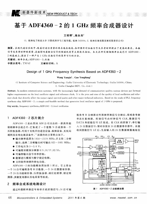
至鉴相器 , 与经 过 N 分 频 的 V O输 出信号进 行相 位 比较 C 锁定 。A 4 6— DF 309的内部 框 图如 图 1 示 。VC 的输 出 所 O 频率如式 () 1所示 :
/ c 一 B× 口 Ⅳ R _( v) J/ () 1
锁相 环是频率合成技 术 的基 础 , 是建 立在相 位负 反馈
a c h r ceii c ff l n e r td v la e c nto ld o clao n ec a a trst sot r ADF4 6 一 r nay e .Th e r t ro M e t lc a e n i y l 3 O9 a e a lz d e g nea o fGS t s co k b s d o
基于ADF4360—2的1GHz频率合成器设计
s t ssc p ADF4 60— 2, asm pl nd f a il e h d t tge e a e oc lo cla o i a H zi o s d yn he i hi 3 i e a e sb e m t o ha n r t sl a s il t rsgn lof1 G spr po e . Key wor ds:fe ue c y he i ; r q n y s nt ss ADF4 0 —2;oc los ilton 36 l a cla i
e c lc h tdr cl fetteo tu in l p cr l u iya doh rmao e h ia dct r.B s do h td f rq e c n eco k t a ietyafc h u p t g a eta p rt n t e jrtc nc ln iao s a e nt esu yo L fe u n y s s i PI
ADF4360-8资料

Integrated Synthesizer and VCOADF4360-8Rev. 0Information furnished by Analog Devices is believed to be accurate and reliable. However, no responsibility is assumed by Analog Devices for its use, nor for any infringements of patents or other rights of third parties that may result from its use. Specifications subject to change without notice. No license is granted by implication or otherwise under any patent or patent rights of Analog Devices. Trademarks and registered trademarks are the property of their respective owners.One Technology Way, P.O. Box 9106, Norwood, MA 02062-9106, U.S.A. Tel: 781.329.4700 Fax: 781.326.8703© 2004 Analog Devices, Inc. All rights reserved.FEATURESOutput frequency range: 65 MHz to 400 MHz 3.0 V to 3.6 V power supply 1.8 V logic compatibility Integer-N synthesizerProgrammable output power level 3-wire serial interface Digital lock detectHardware and software power-down modeAPPLICATIONSSystem clock generation Test equipment Wireless LANs CATV equipmentGENERAL DESCRIPTIONThe ADF4360-8 is an integrated integer-N synthesizer and voltage controlled oscillator (VCO). The ADF4360-8 center frequency is set by external inductors. This allows a frequency range of between 65 MHz to 400 MHz.Control of all the on-chip registers is through a simple 3-wire interface. The device operates with a power supply ranging from 3.0 V to 3.6 V and can be powered down when not in use.FUNCTIONAL BLOCK DIAGRAMCPV VCOREF INCLK DATALEAV DV CER V TUNE C C C NL2L1RF OUT ARF OUT BFigure 1.ADF4360-8Rev. 0 | Page 2 of 24TABLE OF CONTENTSSpecifications.....................................................................................3 Timing Characteristics.....................................................................5 Absolute Maximum Ratings............................................................6 Transistor Count...........................................................................6 ESD Caution..................................................................................6 Pin Configuration and Function Descriptions.............................7 Typical Performance Characteristics.............................................8 Circuit Description.........................................................................10 Reference Input Section.............................................................10 N Counter....................................................................................10 R Counter....................................................................................10 PFD and Charge Pump..............................................................10 MUXOUT and Lock Detect......................................................10 Input Shift Register.....................................................................11 VCO.............................................................................................11 Output Stage................................................................................12 Latch Structure...........................................................................13 Control Latch..............................................................................17 N Counter Latch.........................................................................18 R Counter Latch.........................................................................18 Choosing the Correct Inductance Value.................................19 Fixed Frequency LO...................................................................19 Power-Up.....................................................................................20 Interfacing...................................................................................20 PCB Design Guidelines for Chip Scale Package...........................20 Output Matching........................................................................21 Outline Dimensions.......................................................................22 Ordering Guide.. (22)REVISION HISTORY10/04—Revision 0: Initial VersionADF4360-8Rev. 0 | Page 3 of 24SPECIFICATIONS 1AV DD = DV DD = V VCO = 3.3 V ± 10%; AGND = DGND = 0 V; T A = T MIN to T MAX , unless otherwise noted. Table 1.Parameter B Version Unit Conditions/Comments REF IN CHARACTERISTICS REF IN Input Frequency 10/250 MHz min/max For f < 10 MHz, use a dc-coupled CMOS-compatiblesquare wave, slew rate > 21 V/µs.REF IN Input Sensitivity 0.7/AV DD V p-p min/max AC-coupled. 0 to AV DD V max CMOS-compatible. REF IN Input Capacitance 5.0 pF max REF IN Input Current ±60 µA max PHASE DETECTORPhase Detector Frequency 28 MHz max CHARGE PUMPI CP Sink/Source 3With R SET = 4.7 kΩ. High Value 2.5 mA typ Low Value 0.312 mA typ R SET Range 2.7/10 kΩ I CP Three-State Leakage Current 0.2 nA typ Sink and Source Current Matching 2 % typ 1.25 V ≤ V CP ≤ 2.5 V. I CP vs. V CP 1.5 % typ 1.25 V ≤ V CP ≤ 2.5 V. I CP vs. Temperature 2 % typ V CP = 2.0 V. LOGIC INPUTS V INH , Input High Voltage 1.5 V min V INL , Input Low Voltage 0.6 V max I INH /I INL , Input Current ±1 µA max C IN , Input Capacitance 3.0 pF max LOGIC OUTPUTS V OH , Output High Voltage DV DD – 0.4 V min CMOS output chosen. I OH , Output High Current 500 µA max V OL , Output Low Voltage 0.4 V max I OL = 500 µA. POWER SUPPLIES AV DD 3.0/3.6 V min/V max DV DD AV DD V VCO AV DD AI DD 4 5 mA typDI DD 4 2.5 mA typ I VCO 4, 5 12.0 mA typ I CORE = 5 mA.I RFOUT 43.5 to 11.0 mA typ RF output stage is programmable.Low Power Sleep Mode 47 µA typ Specifications continued on next page. Footnotes on next page.ADF4360-8Rev. 0 | Page 4 of 24Parameter B Version Unit Conditions/CommentsRF OUTPUT CHARACTERISTICS 5Maximum VCO Output Frequency 400 MHz I CORE = 5 mA. Depending on L. See theChoosing the Correct Inductance Value section.Minimum VCO Output Frequency 65 MHz VCO Output Frequency 88/108 MHz min/max L1, L2 = 270 nH. See the Choosing the Correct Inductance Valuesection for other frequency values.VCO Frequency Range 1.2 Ratio F MAX / F MIN VCO Sensitivity 2 MHz/V typ L1, L2 = 270 nH. See the Choosing the Correct Inductance Valuesection for other sensitivity values.Lock Time 6400 µs typ To within 10 Hz of final frequency. Frequency Pushing (Open Loop) 0.24 MHz/V typ Frequency Pulling (Open Loop) 10 Hz typ Into 2.00 VSWR load. Harmonic Content (Second) −16 dBc typHarmonic Content (Third) −21 dBc typOutput Power 5, 7−9/0 dBm typ Using tuned load, programmable in 3 dB steps. See Table 7. Output Power 5, 8 −14/−9 dBm typ Using 50 Ω resistors to V VCO , programmable in 3 dB steps. See Table 7. Output Power Variation ±3 dB typ VCO Tuning Range 1.25/2.5 V min/maxNOISE CHARACTERISTICS 5VCO Phase Noise Performance 9−120 dBc/Hz typ @ 100 kHz offset from carrier. −139 dBc/Hz typ @ 800 kHz offset from carrier. −140 dBc/Hz typ @ 3 MHz offset from carrier. −142 dBc/Hz typ @ 10 MHz offset from carrier.Synthesizer Phase Noise Floor 10−160 dBc/Hz typ @ 200 kHz PFD frequency. −150 dBc/Hz typ @ 1 MHz PFD frequency. −142 dBc/Hz typ @ 8 MHz PFD frequency.Phase Noise Figure of Merit 10−209 dBc/H z typ In-Band Phase Noise 11, 12 −102 dBc/Hz typ @ 1 kHz offset from carrier.RMS Integrated Phase Error 130.09 Degrees typ 100 Hz to 100 kHz.Spurious Signals due to PFDFrequency 12, 14−75 dBc typ Level of Unlocked Signal withMTLD Enabled−70 dBm typ1 Operating temperature range is –40°C to +85°C.2Guaranteed by design. Sample tested to ensure compliance. 3I CP is internally modified to maintain constant loop gain over the frequency range. 4T A = 25°C; AV DD = DV DD = V VCO = 3.3 V. 5Unless otherwise stated, these characteristics are guaranteed for VCO core power = 5 mA. L1, L2 = 270 nH, 470 Ω resistors to GND in parallel with L1, L2. 6Jumping from 88 MHz to 108 MHz. PFD frequency = 200 kHz; loop bandwidth = 10 kHz. 7For more detail on using tuned loads, see Output Matching section. 8Using 50 Ω resistors to V VCO , into a 50 Ω load. 9The noise of the VCO is measured in open-loop conditions. 10The synthesizer phase noise floor is estimated by measuring the in-band phase noise at the output of the VCO and subtracting 20 log N (where N is the N divider value). The phase noise figure of merit subtracts 10 log (PFD frequency). 11The phase noise is measured with the EVAL-ADF4360-xEB1 Evaluation Board and the HP 8562E Spectrum Analyzer. The Spectrum Analyzer provides the REFIN for the synthesizer; offset frequency = 1 kHz. 12f REFIN = 10 MHz; f PFD = 200 kHz; N = 1000; Loop B/W = 10 kHz. 13f REFIN = 10 MHz; f PFD = 1 MHz; N = 120; Loop B/W = 100 kHz. 14The spurious signals are measured with the EVAL-ADF4360-xEB1 Evaluation Board and the HP 8562E Spectrum Analyzer. The Spectrum Analyzer provides the REFIN for the synthesizer; f REFOUT = 10 MHz @ 0 dBm.ADF4360-8Rev. 0 | Page 5 of 24TIMING CHARACTERISTICSAV DD = DV DD = V VCO = 3.3 V ± 10%; AGND = DGND = 0 V; 1.8 V and 3 V logic levels used; T A = T MIN to T MAX , unless otherwise noted. Table 2.Parameter Limit at T MIN to T MAX (B Version) Unit Test Conditions/Comments t 1 20 ns min LE Setup Timet 2 10 ns min DATA to CLOCK Setup Time t 3 10 ns min DATA to CLOCK Hold Time t 4 25 ns min CLOCK High Duration t 5 25 ns min CLOCK Low Duration t 6 10 ns min CLOCK to LE Setup Time t 720ns minLE Pulse WidthCLOCKDATALELEFigure 2. Timing DiagramADF4360-8Rev. 0 | Page 6 of 24ABSOLUTE MAXIMUM RATINGST A = 25°C, unless otherwise noted. Table 3.Parameter RatingAV DD to GND 1 −0.3 V to +3.9 VAV DD to DV DD −0.3 V to +0.3 VV VCO to GND −0.3 V to +3.9 VV VCO to AV DD −0.3 V to +0.3 VDigital I/O Voltage to GND −0.3 V to V DD + 0.3 VAnalog I/O Voltage to GND −0.3 V to V DD + 0.3 VREF IN to GND −0.3 V to V DD + 0.3 V Operating Temperature Range −40°C to + 85°C Storage Temperature Range −65°C to +150°C Maximum Junction Temperature 150°C CSP θJA Thermal ImpedancePaddle Soldered 50°C/W Paddle Not Soldered 88°C/W Lead Temperature, SolderingVapor Phase (60 sec) 215°CInfrared (15 sec) 220°C1GND = AGND = DGND = 0 V.Stresses above those listed under Absolute Maximum Ratings may cause permanent damage to the device. This is a stress rating only; functional operation of the device at these or any other conditions above those listed in the operational sectionsof this specification is not implied. Exposure to absolute maxi-mum rating conditions for extended periods may affect device reliability.This device is a high performance RF integrated circuit with an ESD rating of <1 kV , and it is ESD sensitive. Proper precautions should be taken for handling and assembly.TRANSISTOR COUNT 12543 (CMOS) and 700 (Bipolar)ESD CAUTIONESD (electrostatic discharge) sensitive device. Electrostatic charges as high as 4000 V readily accumulate on thehuman body and test equipment and can discharge without detection. Although this product features proprie-tary ESD protection circuitry, permanent damage may occur on devices subjected to high energy electrostatic discharges. Therefore, proper ESD precautions are recommended to avoid performance degradation or loss of functionality.ADF4360-8Rev. 0 | Page 7 of 24PIN CONFIGURATION AND FUNCTION DESCRIPTIONSCPGND AV DD AGND RF OUT A RF OUT B V VCO DATA CLK REF IN DGND C N R SETV T U N E A G N D L 1L 2A G N D C C C PC EA G N DD V D DM U X O U TL E04763-003Figure 3. Pin ConfigurationADF4360-8Rev. 0 | Page 8 of 24TYPICAL PERFORMANCE CHARACTERISTICS–150–120–130–140–70–60–90–100–110–80–40–501001k10k 100k1M10MFREQUENCY OFFSET (Hz)O U T P U T P O W E R (d B )04763-004Figure 4. Open-Loop VCO Phase Noise, L1, L2 = 560 nH–150–125–130–120–135–140–145–85–80–95–100–105–110–115–90–70–751001k10k 100k1M 10MFREQUENCY OFFSET (Hz)O U T P U T P O W E R (d B )04763-005Figure 5. VCO Phase Noise, 65 MHz, 1 MHz PFD, 100 kHz Loop BandwidthO U T P U T P O W E R (d B )–90–80–70–60–50–40–30–20–100–2kHz–1kHz65MHz 1kHz 2kHzFigure 6. Close-In Phase Noise at 65 MHz (1 MHz Channel Spacing)O U T P U T P O W E R (d B )–90–80–70–60–50–40–30–20–100–1.1MHz–0.55MHz65MHz 0.55MHz 1.1MHzFigure 7. Reference Spurs at 65 MHz(1 MHz Channel Spacing, 100 kHz Loop Bandwidth)–150–120–130–140–70–60–90–100–110–80–40–501001k10k 100k1M10MFREQUENCY OFFSET (Hz)O U T P U T P O W E R (d B )04763-008Figure 8. Open-Loop VCO Phase Noise, L1, L2 = 110 nH–150–125–130–120–135–140–145–85–80–95–100–105–110–115–90–70–751001k10k 100k1M 10MFREQUENCY OFFSET (Hz)O U T P U T P O W E R (d B )04763-009Figure 9. VCO Phase Noise, 160 MHz, 1 MHz PFD, 100 kHz Loop BandwidthADF4360-8Rev. 0 | Page 9 of 24O U T P U T P O W E R (d B )–90–80–70–60–50–40–30–20–100Figure 10. Close-In Phase Noise at 160 MHz (1 MHz Channel Spacing)O U T P U T P O W E R (d B )–90–80–70–60–50–40–30–20–10–1.1MHz–0.55MHz160MHz0.55MHz1.1MHzFigure 11. Reference Spurs at 160 MHz(1 MHz Channel Spacing, 100 kHz Loop Bandwidth)–150–120–130–140–70–60–90–100–110–80–40–501001k10k 100k1M10MFREQUENCY OFFSET (Hz)O U T P U T P O W E R (d B )04763-012Figure 12. Open-Loop VCO Phase Noise, L1, L2 = 18 nH–150–125–130–120–135–140–145–85–80–95–100–105–110–115–90–70–751001k10k 100k1M 10MFREQUENCY OFFSET (Hz)O U T P U T P O W E R (dB )04763-013Figure 13. VCO Phase Noise, 400 MHz, 1 MHz PFD, 100 kHz Loop BandwidthO U T P U T P O W E R (d B )Figure 14. Close-In Phase Noise at 400 MHz (1 MHz Channel Spacing)O U T P U T P O W E R (d B )–90–80–70–60–50–40–30–20–100–1.1MHz–0.55MHz400MHz 0.55MHz 1.1MHzFigure 15. Reference Spurs at 400 MHz(1 MHz Channel Spacing, 100 kHz Loop Bandwidth)ADF4360-8Rev. 0 | Page 10 of 24CIRCUIT DESCRIPTIONREFERENCE INPUT SECTIONThe reference input stage is shown in Figure 16. SW1 and SW2 are normally closed switches. SW3 is normally open. When power-down is initiated, SW3 is closed, and SW1 and SW2 are opened. This ensures that there is no loading of the REF IN pin on power-down.04763-016POWER-DOWNFigure 16. Reference Input StageN COUNTERThe CMOS N counter allows a wide division ratio in the PLL feedback counter. The counters are specified to work when the VCO output is 400 MHz or less. To avoid confusion, this is referred to as the B counter. It makes it possible to generate output frequencies that are spaced only by the reference frequency divided by R . The VCO frequency equation isR f B f REFIN VCO /×=where:f VCO is the output frequency of the VCO. B is the preset divide ratio of the binary 13-bit counter (3 to 8191).f REFIN is the external reference frequency oscillator.R COUNTERThe 14-bit R counter allows the input reference frequency to be divided down to produce the reference clock to the phase frequency detector (PFD). Division ratios from 1 to 16,383 are allowed.PFD AND CHARGE PUMPThe PFD takes inputs from the R counter and N counter (N = BP + A ) and produces an output proportional to the phase and frequency difference between them. Figure 17 is a simplified schematic. The PFD includes a programmable delay element that controls the width of the antibacklash pulse. This pulse ensures that there is no dead zone in the PFD transfer function and minimizes phase noise and reference spurs. Two bits in the R counter latch, ABP2 and ABP1, control the width of the pulse (see Table 9).VFigure 17. PFD Simplified Schematic and Timing (In Lock)MUXOUT AND LOCK DETECTThe output multiplexer on the ADF4360 family allows the user to access various internal points on the chip. The state of MUXOUT is controlled by M3, M2, and M1 in the function latch. The full truth table is shown in Table 7. Figure 18 shows the MUXOUT section in block diagram form.R COUNTER OUTPUT N COUNTER OUTPUTDIGITAL LOCK DETECT DGNDMUXOUTDV 04763-018Figure 18. MUXOUT CircuitLock DetectThe correct band is chosen automatically by the band select logic at power-up or whenever the N counter latch is updated. It is important that the correct write sequence be followed at power-up. This sequence is MUXOUT can be programmed for one type of lock detect. Digital lock detect is active high. When LDP in the R counter latch is set to 0, digital lock detect is set high when the phase error on three consecutive phase detector cycles is less than 15 ns. 1. R counter latch With LDP set to 1, five consecutive cycles of less than 15 ns phase error are required to set the lock detect. It stays set high until a phase error of greater than 25 ns is detected on any subsequent PD cycle.2. Control latch3. N counter latchDuring band select, which takes five PFD cycles, the VCO V TUNE is disconnected from the output of the loop filter and connected to an internal reference voltage.INPUT SHIFT REGISTERThe ADF4360 family’s digital section includes a 24-bit input shift register, a 14-bit R counter, and an 18-bit N counter comprised of a 5-bit A counter and a 13-bit B counter. Data is clocked into the 24-bit shift register on each rising edge of CLK. The data is clocked in MSB first. Data is transferred from the shift register to one of four latches on the rising edge of LE. The destination latch is determined by the state of the two control bits (C2, C1) in the shift register. These are the two LSBs, DB1 and DB0, shown in Figure 2.01.00.52.52.01.53.53.080859010095105115110FREQUENCY (MHz)V T U N E (V )04763-019The truth table for these bits is shown in Table 5. Table 6 shows a summary of how the latches are programmed. Note that the test modes latch is used for factory testing and should not be programmed by the user. Table 5. C2 and C1 Truth TableFigure 19. Frequency vs. V TUNE , ADF4360-8, L1 and L2 = 270 nHControl BitsC2 C1 Data Latch 0 0 Control Latch 0 1 R Counter 1 0 N Counter (B) 11Test Modes LatchThe R counter output is used as the clock for the band select logic and should not exceed 1 MHz. A programmable divider is provided at the R counter input to allow division by 1, 2, 4, or 8 and is controlled by Bits BSC1 and BSC2 in the R counter latch. Where the required PFD frequency exceeds 1 MHz, the divide ratio should be set to allow enough time for correct band selection.VCOThe VCO core in the ADF4360 family uses eight overlapping bands, as shown in Figure 19, to allow a wide frequency range to be covered without a large VCO sensitivity (K V ) and resultant poor phase noise and spurious performance.After band selection, normal PLL action resumes. The value of K V is determined by the value of inductors used (see theChoosing the Correct Inductance Value section). The ADF4360 family contains linearization circuitry to minimize any variation of the product of I CP and K V .The operating current in the VCO core is programmable in four steps: 2.5 mA, 5 mA, 7.5 mA, and 10 mA. This is controlled by Bits PC1 and PC2 in the control latch.OUTPUT STAGEThe RF OUT A and RF OUT B pins of the ADF4360 family are connected to the collectors of an NPN differential pair driven by buffered outputs of the VCO, as shown in Figure 20. To allow the user to optimize the power dissipation versus the output power requirements, the tail current of the differential pair is programmable via Bits PL1 and PL2 in the control latch. Four current levels may be set: 3.5 mA, 5 mA, 7.5 mA, and 11 mA. These levels give output power levels of −9 dBm, −6 dBm,−3 dBm, and 0 dBm, respectively, using the correct shunt inductor to V DD and ac coupling into a 50 Ω load. Alternatively, both outputs can be combined in a 1 + 1:1 transformer or a 180° microstrip coupler (see the Output Matching section). If the outputs are used individually, the optimum output stage consists of a shunt inductor to V DD.Another feature of the ADF4360 family is that the supply current to the RF output stage is shut down until the part achieves lock as measured by the digital lock detect circuitry. This is enabled by the Mute-Till-Lock Detect (MTLD) bit in the control latch.RF OUT A RF OUT BFigure 20. Output Stage ADF4360-8LATCH STRUCTURETable 6 shows the three on-chip latches for the ADF4360 family. The two LSBs decide which latch is programmed. Table 6. Latch StructureCONTROL LATCHN COUNTER LATCHR COUNTER LATCHTable 7. Control LatchTable 8. N Counter LatchTable 9. R Counter LatchCONTROL LATCHWith (C2, C1) = (0,0), the control latch is programmed. Table 7 shows the input data format for programming the control latch. Power-DownDB21 (PD2) and DB20 (PD1) provide programmable power-down modes.In the programmed asynchronous power-down, the device powers down immediately after latching a 1 into Bit PD1,with the condition that PD2 has been loaded with a 0. In the programmed synchronous power-down, the device power-down is gated by the charge pump to prevent unwanted frequency jumps. Once the power-down is enabled by writing a 1 into Bit PD1 (on the condition that a 1 has also been loaded to PD2), the device goes into power-down on the second rising edge of the R counter output, after LE goes high. When the CE pin is low, the device is immediately disabled regardless of the state of PD1 or PD2.When a power-down is activated (either synchronous or asynchronous mode), the following events occur:•All active dc current paths are removed.•The R, N, and timeout counters are forced to their load state conditions.•The charge pump is forced into three-state mode.•The digital lock detect circuitry is reset.•The RF outputs are debiased to a high impedance state. •The reference input buffer circuitry is disabled.•The input register remains active and capable of loading and latching data. Charge Pump CurrentsCPI3, CPI2, and CPI1 in the ADF4360 family determine Current Setting 1.CPI6, CPI5, and CPI4 determine Current Setting 2. See the truth table in Table 7.Output Power LevelBits PL1 and PL2 set the output power level of the VCO. See the truth table in Table 7.Mute-Till-Lock DetectDB11 of the control latch in the ADF4360 family is the Mute-Till-Lock Detect bit. This function, when enabled, ensures that the RF outputs are not switched on until the PLL is locked.CP GainDB10 of the control latch in the ADF4360 family is the Charge Pump Gain bit. When it is programmed to 1, Current Setting 2 is used. When it is programmed to 0, Current Setting 1 is used. Charge Pump Three-StateThis bit puts the charge pump into three-state mode when programmed to a 1. It should be set to 0 for normal operation. Phase Detector PolarityThe PDP bit in the ADF4360 family sets the phase detector polarity. The positive setting enabled by programming a 1 is used when using the on-chip VCO with a passive loop filter or with an active noninverting filter. It can also be set to 0, which is required if an active inverting loop filter is used.MUXOUT ControlThe on-chip multiplexer is controlled by M3, M2, and M1. See the truth table in Table 7.Counter ResetDB4 is the counter reset bit for the ADF4360 family. When this is 1, the R counter and the A, B counters are reset. For normal operation, this bit should be 0.Core Power LevelPC1 and PC2 set the power level in the VCO core. The recom-mended setting is 5 mA. See the truth table in Table 7.N COUNTER LATCHTable 8shows the input data format for programming theN counter latch.Reserved BitsDB2 to DB7 are spare bits and have been designated as Reserved. They should be programmed to 0.B Counter LatchB13 to B1 program the B counter. The divide range is 3 (00.....0011) to 8191 (11....111).Overall Divide RangeThe overall VCO feedback divide range is defined by B.CP GainDB21 of the N counter latch in the ADF4360 family is the charge pump gain bit. When this is programmed to 1, Current Setting 2 is used. When programmed to 0, Current Setting 1 is used. This bit can also be programmed through DB10 of the control latch. The bit always reflects the latest value written to it, whether this is through the control latch or the N counter latch. R COUNTER LATCHWith (C2, C1) = (0, 1), the R counter latch is programmed. Table 9shows the input data format for programming theR counter latch.R CounterR1 to R14 set the counter divide ratio. The divide range is1 (00......001) to 16383 (111......111).Antibacklash Pulse WidthDB16 and DB17 set the antibacklash pulse width.Lock Detect PrecisionDB18 is the lock detect precision bit. This bit sets the number of reference cycles with less than 15 ns phase error for entering the locked state. With LDP at 1, five cycles are taken; with LDP at 0, three cycles are taken.Test Mode BitDB19 is the test mode bit (TMB) and should be set to 0. With TMB = 0, the contents of the test mode latch are ignored and normal operation occurs as determined by the contents of the control latch, R counter latch, and N counter latch. Note that test modes are for factory testing only and should not be programmed by the user.Band Select ClockThese bits set a divider for the band select logic clock input. The output of the R counter is by default the value used to clock the band select logic, but if this value is too high (>1 MHz), a divider can be switched on to divide the R counter output to a smaller value (see Table 9).Reserved BitsDB23 to DB22 are spare bits that have been designated as Reserved. They should be programmed to 0.CHOOSING THE CORRECT INDUCTANCE VALUEThe ADF4360-8 can be used at many different frequencies simply by choosing the external inductors to give the correct output frequency. Figure 21 shows a graph of both minimum and maximum frequency versus the external inductor value. The correct inductor should cover the maximum and minimum frequencies desired. The inductors used are 0603 CS or 0805 CS type from Coilcraft. To reduce mutual coupling, the inductors should be placed at right angles to one another.The lowest center frequency of oscillation possible is approxi-mately 65 MHz, which is achieved using 560 nH inductors. This relationship can be expressed by()EXT O L F +=nH 0.9pF 9.32π10150501003502503002004504000100200300400600500INDUCTANCE (nH)F R E Q U E N C Y (M H z )04763-025Figure 21. Output Center Frequency vs. External Inductor ValueWhere F O is the center frequency and L EXT is the external induc-tance. The approximate value of capacitance at the midpoint of the center band of the VCO is 9.3 pF, and the approximate value of internal inductance due to the bond wires is 0.9 nH. The VCO sensitivity is a measure of the frequency change versus the tuning voltage. It is a very important parameter for the low-pass filter. Figure 22 shows a graph of the tuning sensitivity (in MHz/V) versus the inductance (nH). It can be seen that as the inductance increases, the sensitivity decreases. This relationship can be derived from the equation above, i.e., since the induc-tance has increased, the change in capacitance from the varactor has less of an effect on the frequency.421086120100200300400600500INDUCTANCE (nH)S E N S I T I V I T Y (M H z /V)04763-026Figure 22. Tuning Sensitivity (in MHz/V) vs. Inductance (nH)FIXED FREQUENCY LOFigure 23 shows the ADF4360-8 used as a fixed frequency LO at 200 MHz. The low-pass filter was designed using ADIsimPLL for a channel spacing of 2 MHz and an open-loop bandwidth of 100 kHz. The maximum PFD frequency of the ADF4360-8 is 8 MHz. Since using a larger PFD frequency allows the use of a smaller N, the in-band phase noise is reduced to as low as possible, −109 dBc/Hz. The typical rms phase noise (100 Hz to 100 kHz) of the LO in this configuration is 0.09°. The reference frequency is from a 16MHz TCXO from Fox; thus, an R value of 2 is programmed. Taking into account the high PFD frequency and its effect on the band select logic, the band select clock divider is enabled. In this case, a value of 8 is chosen. A verysimple shunt inductor and dc blocking capacitor complete the RF output stage.LOCKFigure 23. Fixed Frequency LO。
基于ADF4360-3的本振信号发生器的设计
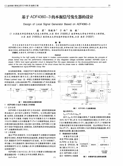
12 工 作 原 理 _
[ 尸}日私 ] R xr E
() 2
其 中 ,。 为 V f。 v CO 的输 出 频 率 ; 前 置 分 频 器 的 预 先模 值 P为 (/ 、 6 1 8 9 1 / 7等 )B 为 1 计 数 器 预 设 分 频 比 ( - 1 1 ; 为 ; 3位 3 8 9 )A
《 业 控 制 计 算 机 } 0 2年第 2 工 21 5卷 第 2期
3 1
基于 A F 3 0 3的本振信号发生器的设计 D 46—
De i f L c lS g a n r t r B s d o sgn o o a i n lGe e a o a e n ADF 3 0- 46 3
盛
君 ’ 陈毅 华 于 玮 。 陆 毅 ’
( 江 苏技 术师 范 学院 电气信 息工程 学 院, 苏 常 州 2 3 0 ; 南京 邮电大 学 电子 科 学与工程 学院 , 1 江 10 0 2 江 苏 南京 2 0 0 ; 南京林 业 大学信 息科 学技 术学 院 , 苏 南京 2 0 3 ) 1033 江 1 0 7
ph s l k d lop nd h pef r a e oc e o a t e ro man e haacer t s c c r t i i of ul it a e v t e—co tol d sc f l negrt d ol y ag n r l os l t ADF 3 e ciaor l 4 60— a a 3.nd se y .G Hz o l i al en  ̄ o cr i i de i e Th n hi t ad 19 lca sgn g er r i t s cu sgn d. e t s pap ab ats on t e s rct e。ero man e n appi erel or e h tu ur p f r c a d l — c t o h r hi L s l h mea ur f te i i h ws t tt e ph e oie s -83 ai on ft e co e c p.a t te y s e o h cr t o ha h as n s i cu s dBc /Hz 1 k @ 00 Hz.
基于ADF4360系列的小型化频率综合器设计
2 设 计 原 理
A F 3 0内部 的鉴 相器 、 D46 电荷 泵 和可 编程 分 频 器 延承 了 A I 司 A F 1 X系列 P L器 件 的性 能 D公 D40 L 和特点 。A F 1 X系 列 P L芯 片最 大 的创 新 在 于 D 40 L 集成 V O于芯 片中。但需 要注 意 的是 , 我们通 常 C 与 使用 的 V O不 同, 芯片 内置 V O 的输 出频 率 与 C 该 C
LN Q a I io—l i
( o tw s C iaIstt o l t ncT cn l y C eg u6 3 , hn ) S uh et hn tu f e r i eh o g , h nd 0 6 C ia n i e E co o 1 0
Ab t a t: c r i g t h n fmi it rz t n o e u nc y te ie , d sg x mp e b s d o sr c Ac o d n o t e we d o n au ia i f f q e y s nh sz r a e in e a l a e n o r
围 , 设计 时通过 调整 外 部 电感 值 确 定实 际输 出频 在
率范 围 , 最 新 产 品 A F 3 0—9在 A F 3 0—8 而 D 46 D 46
的基 础上 在其 V O输 出端增加 可编 程分 频器 ( C 分频 次数 为 2~ 1 ) 从 而扩 展 了输 出带 宽 ( 3次 , 扩展 后带 宽可 达 1 1~ 0 z , 得设计 更 为灵 活 , . 4 0MH ) 使 设计 电 路得 到进 一 步 简 化 。本 文将 介 绍 采用 A I 司 的 D公 A F 3 0系列 P L芯 片 实现 小 型 化 频 率 综 合 器 的 D 46 L
基于ADF4360-1的2.4G频率合成器设计
基于ADF4360-1的2.4G频率合成器设计摘要:该文通过高性能、低功耗的8位ATmega8微处理器产生控制信号,利用美国ADI公司生产的锁相环芯片ADF4360-1,设计了一个稳定的2.4GHz本振信号源电路模块,可广泛应用于电视,仪器,通信等领域。
文中详细介绍了系统中核心芯片的性能、结构以及应用方法,设计出了完整的硬件电路并对电路的各个参数进行了评估,结果基本上符合要求。
关键词:ATmega8 ADF4360-1锁相环频率合成本振信号源在现代无线电通信及相关领域中,为确保通信的稳定和可靠,对通信设备的频率准确度和稳定度提出了越来越高的要求。
与LC振荡电路“跑频”严重相比,晶体振荡电路具有可微调的稳定频率,但变化范围小,频率值不高。
频率合成技术是指将一个或少量的高稳定度、高准确度的标准频率作为参考频率,经过相应的信号处理过程,从而获得大量离散的具有同一稳定度和准确度的信号频率。
主要有三种合成方法:直接模拟合成、锁相环合成以及直接数字合成。
1 锁相式频率合成器的基本原理锁相环路(PLL)具有较为突出的优点:频率在一定范围内可调;数字化接口;能实现快速准确的跳频通信;抗干扰能力强。
锁相环频率合成器通过锁相环完成频率的加减乘除运算,是一种建立在相位负反馈基础上的闭环控制系统,对相位噪声和杂散具有很好的抑制作用。
原理图如图1所示,主要由鉴相器、环路滤波器和压控振荡器组成。
外部晶振提供的参考频率信号与压控振荡器的输出频率经程序N分频后在鉴相器内进行相位比较,产生误差控制电压,再经环路滤波器滤除误差信号中的噪声和高频分量,最后输出的直流脉冲电压控制压控振荡器产生所需的振荡频率。
通过锁相式频率合成实现的频率源应用广泛于通信、电视等电子设计领域,重点用于以下三方面:接收机本地振荡;发射机载波信号;信号发生器。
ADI公司生产的ADF4360-1内置可编程分频器,具有电荷泵电流编程功能,可应用于无线射频通信系统,是一款性价比很高的电荷泵锁存芯片。
L波段宽带上变频器的设计与实现
L波段宽带上变频器的设计与实现张洪涛;张伟;杜欣【摘要】介绍了一种L波段宽带上变频器的设计方案与电路实现,该方案可有效降低杂散抑制难度.首先介绍了该方案的电路结构和仿真分析,并给出了关键电路本振和频综的实现方法,最后给出了模块的实测结果.仿真和实测结果表明该模块实现了预期指标需求.%In this paper, a design scheme of wide-band up-converter in L band and the designing method of the circuit are presented, which reduce the difficulty of spurious suppression effectively. Firstly, the paper presents the circuit structure and the circuit simulation analysis, and gives the designing method of the significant circuit that can produce the local oscillation and frequency synthesis. Finally, the actual measurement results of the module is presented. The simulation and measurement results indicate that the module meets the needs of the anticipated specifications.【期刊名称】《现代电子技术》【年(卷),期】2012(035)015【总页数】3页(P90-92)【关键词】频率合成器;杂散抑制;本振泄露;超外差【作者】张洪涛;张伟;杜欣【作者单位】北京天航信民航通信网络发展有限公司,北京100193;北京天航信民航通信网络发展有限公司,北京100193;北京天航信民航通信网络发展有限公司,北京100193【正文语种】中文【中图分类】TN773-340 引言IF/L波段上变频模块是卫星通信中的重要模块,因其频带较宽,需采用二次变频的架构实现;为防止系统杂散对其他无线信号的干扰,对杂散抑制度指标要求较高,宽带滤波器的设计往往是设计中的难点。
锁相环常见问题解答讲解
ADI官网下载了个资料,对于PLL学习和设计来说都非常实用的好资料,转发过来,希望对大家有帮助(原文链接/zh/content/cast_faq_PLL/fca.html#faq_pll_01)∙参考晶振有哪些要求?我该如何选择参考源?∙请详细解释一下控制时序,电平及要求?∙控制多片PLL芯片时,串行控制线是否可以复用?∙请简要介绍一下环路滤波器参数的设置?∙环路滤波器采用有源滤波器还是无源滤波器?∙PLL对于VCO有什么要求?以及如何设计VCO输出功率分配器?∙如何设置电荷泵的极性?∙锁定指示电路如何设计?∙PLL对射频输入信号有什么要求?∙PLL芯片对电源的要求有哪些?∙内部集成了VCO的ADF4360-x,其VCO中心频率如何设定?∙锁相环输出的谐波?∙锁相环系统的相位噪声来源有哪些?减小相位噪声的措施有哪些?∙为何我测出的相位噪声性能低于ADISimPLL仿真预期值?∙锁相环锁定时间取决于哪些因素?如何加速锁定?∙为何我的锁相环在做高低温试验的时候,出现频率失锁?∙非跳频(单频)应用中,最高的鉴相频率有什么限制?∙频繁地开关锁相环芯片的电源会对锁相环有何影响?∙您能控制PLL芯片了么?,R分频和N分频配置好了么?∙您的晶振输出功率有多大?VCO的输出功率有多大?∙您的PFD鉴相极性是正还是负?∙您的VCO输出频率是在哪一点?最低频率?最高频率?还是中间的某一点?VCO 的控制电压有多大?∙您的PLL环路带宽和相位裕度有多大?∙评价PLL频率合成器噪声性能的依据是什么?∙小数分频的锁相环杂散的分布规律是什么?∙到底用小数分频好还是整数分频好?∙ADI提供的锁相环仿真工具ADISimPLL支持哪些芯片,有什么优点?∙分频–获得高精度时钟参考源?∙PLL,VCO闭环调制,短程无线发射芯片?∙PLL,VCO开环调制?∙时钟净化----时钟抖动(jitter)更小?∙时钟恢复(Clock Recovery)?问题:参考晶振有哪些要求?我该如何选择参考源?答案:波形:可以使正弦波,也可以为方波。
基于ADF4360—8的频率合成系统
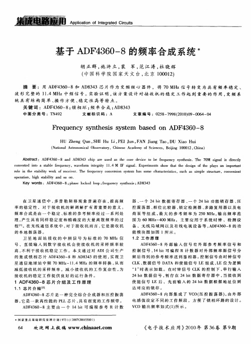
F e ue y s n he i y t m s d o r q nc y t ss s s e ba e n ADF4 6 — 3 0—8
的本地 振荡 器 。
荷 泵 等 组 成 , 大 的 参 考 频 率 为 2 0 MHz 输 出 频 率 范 最 5 ,
围 为 6 0 MHz 4 0 MH , 主 要 应 用 于 系 统 时 钟 、检 测 设 - 0 z 备 、无 线 局 域 网 以及 有 线 电视 设 备 等 , D 4 6 — A F 3 0 8的 功
c n e t d nt a tb e r qu n y,wa eo m i t g t 11 4 M I sg 1 Ex rm e t s w t t h de in f t p a s n mpo tn o v re i o sa l fe e c v fr n e r y . i F ina . pe i n s ho ha t e sg o he l y a i ra t r l i t e t b lt r o e e v r oe n h sa iiy wo k f r c i e .The r q n y o v ri n y tm ha s m e ha a trsi s s h s i e tu t e, c n e i n fe ue c c n es o s se s o c r ce tc , uc a smpl sr cur i o v ne t
o e a in,h g tb l y a d S n p rt o ih sa i t n O o . i Ke y wo d r s: A 4 6 -8; h s o k d l o fe u n y s n h ss AD8 4 DF 3 0 p a e l c e o p;r q e c y t e i ; 33
锁相环常见问题解答
29
A
ADI 公司已经发布产品
最大射频 输入频率 范围 型号
AD809 ADF4001 ADF4002 ADF4007 ADF4106 ADF4107
PLL 常见问题解答
输出频 率范围 (MHz)
155.52 MHz -
归一化 相 位 噪 声 (dBc/Hz)
-219 -214 -222 -219 -219 -219
最大参考 输入频率 (MHz)
19.44 104 300 240 300 250
电源电流 预分频模数
n/a n/a N counter = 8/16/32/64 16/17, 32/33, 64/65, 8/9 16/17, 32/33, 64/65, 8/9 16/17, 32/33, 4/5, 64/65,
锁相环常见问题解答
编写人 版本号
CAST (Y/D) V1.1
-----------------------------------------------------------------------------------------------------------本报告为 Analog Devices Inc. (ADI) 中国技术支持中心专用,ADI 可以随时修改本 报告而不用通知任何使用本报告的人员。 如有任何问题请与 china.support@ 联系。 ------------------------------------------------------------------------------------------------------------
目
1 2
录
3
4
ADI公司锁相环产品概述.................................
基于ADF4360-0的2.4 GHz射频信号源设计

基于ADF4360-0的2.4 GHz射频信号源设计作者:陈肇南来源:《机电信息》2020年第03期摘要:在现代无线通信系统中,对数据的高速无线传输需求日益增加,而且无线路由器、蓝牙等技术也在生活中有着广泛的应用,故而对于2.4 GHz频段的信号源的需求越来越多。
但是,除了一些在2.4 GHz频带产生信号的高端信号发生器外,平常使用的信号源很少会涉及2.4 GHz这一频段,因此,为满足科学和教育的需要,设计和研发了一款便宜可靠的2.4 GHz 射频信号发生器,并对其实现与仿真进行了介绍。
关键词:2.4 GHz;射频信号源;压控振荡器0 引言在电子通信系统中,如果想实现更大的带宽,我们只能通过使用更高的载波频率来满足要求。
在无线通信中,需要使用天线来发送和接收信号,工作频率越高,天线的尺寸就越小,满足了小型化的通信要求。
由于整体趋势是朝着宽频率覆盖、高精度、多功能以及自动化和智能化的方向发展,当今电子领域更多的电子通信系统使用更高频率的射频,这促进了丰富的射频应用,并带动了射频技术的进一步发展[1]。
1 相关原理概述压控振荡器(VCO)的定义为输出频率对应于输入控制电压的振荡电路,其在无线测量仪器和通信系统电路中使用广泛。
VCO作为锁相环电路和时钟恢复电路的主要组成部分,其性能可以直接影响到频率源的性能,这又决定了整个系统输出信号的稳定性、噪声特性和谐波抑制特性。
正是由于这些因素,VCO在电子通信技术领域发挥着重要作用。
因其具有电子调谐、紧凑、低功耗和高可靠性等优点,关于VCO的研究很多。
近年来,随着集成电路的快速发展,VCO的设计和实现逐渐融入其中,集成式VCO使用方便、性能稳定[2]。
2 关于ADF4360-0的介绍在ADF4360系列锁相环中,我們需要在芯片ADF4360-7和ADF4360-8的外部去设置两个电感,作用是方便确定VCO所处频段,这个操作步骤就相当于从芯片中将VCO的电感移除。
基于ADF4360—8的锁相环频率合成器的设计与实现

s y n he t s i z e r r e a c h e s 2 . 1 6 V( p e a k - p e a k ) , b e i n g a b l e t o d i r e c t i v e l y d r i v e t h e T T L c i r c u i t . T h e t e s t r e s u l t s s h o w t h a t
谢 亮 ,芦旭 ,吴成 英 。 ,杨 建青 ,樊战友
( 1 .中国科学院 国家授时 中心 ,西安 7 1 0 6 0 0 ; 2 .中国科学 院研究生 院 ,北京 1 0 0 0 3 9 ;
3 .湖北民族大学 ,恩施 4 4 5 0 0 0 )
摘要:为满足工程需要 ,设计并 实现 了一种基 于锁相环 芯片 A D F 4 3 6 0 — 8 的低噪声 高稳定度频率
he t o u t p u t s i g n a l s o f t h e r f e q u e n c y s y n he t s i z e r re a c h ra a c t e r i z e d b y g o o d s t a b i l i y, t l o w n o i s e a n d h i g h a mp l i t u d e .
XI E Li a n g 一, LU Xu 一, W U Che n g . yi n g , YAN G J i a n. q i n g , F AN Zh a n. yo u
f 1 . Na t i o n a l T i me S e r v i c e Ce n t e r , Ch i n e s eAc a d e my o f S c i e n c e s , Xi a l l 7 1 0 6 0 0 , Ch i n a ;
锁相频率合成芯片ADF4360_0及其应用
图 1 锁 相 环 频 率 合 成 器 原 理 框 图
收到本文时间 :0 7年 2月 2 20 8日 作者简介 : 叶碧霞 , , 女 硕士研究生 , 研究 方向 : 射频 电路 。董天临 , 教授 。
维普资讯
10 4
计算机 与数字工程
( 4 i 、 编 程 A( bt 预 置 、 1 bt 计 数 器及 1 bt 可 ) 5i ) B( 3 i )
2 锁相环频率合 成芯片工作原理及
主要 性 能
2 1 工作 原理 .
一
双模前 置 ( / P P+1 分 频器 。A F30 0的 内部 电 ) D 46 _ 路 结构 如 图 2所 示 。 由 于此 芯 片 内 部 包 含 V O, C 因此 只需外 接环 路 滤 波器 即可 组 成 一个 完 整 的锁
F u =F E N/ O v RF R
个典 型 的频 率 合成 器 通 常 由鉴 相 器 ( D) P 、
环路滤 波器 ( P 、 控 振 荡 器 ( C 和 可 变 程 序 L )压 V O) 分频器 组成 , 其原 理框 图如 图 1 示 。 所
R
3B d m, 并 —DD/_ I1R IT 围是 一1d m ~ 一6 B 电 荷 泵 电 流 可 编 程 , —IE 广 F R E『 c— Ⅵ _]f HF R. 01 R 】 I 1 u 『L 1『 ’ v 定 检 测 , 有 硬 件 和 软 件 掉 电模 式 , 时 可 三 线 具 同
相环路 , 设计简单 , 成本较低 。
A F 3 0—0工 作 频 率 范 围 是 20 MH D 46 4 0 z到 2 2 MH , 7 5 z 工作 电压 为 3 0 一 、 V, 编 程 双 模 .V 3 6 可 预分 频 为 8 9 1/ 7 3 / 3 输 出功 率 可 编 程 范 / ,6 1 ,23 , 可 编 程反 后 冲脉 冲 宽 度 , 够 进 行 模 拟 和 数 字 锁 能
半导体传感器ADF4360-4BCPZ中文规格书

ADF4116/ADF4117/ADF4118Rev. D | Page 13 of 28PHASE FREQUENCY DETECTOR (PFD) AND CHARGE PUMP The PFD takes inputs from the R counter and N counter and produces an output proportional to the phase and frequency difference between them. Figure 28 is a simplified schematic of the PFD. The PFD includes a fixed delay element that sets the width of the antibacklash pulse. This is typically 3 ns. This pulseensures that there is no dead zone in the PFD transfer function and gives a consistent reference spur level.00392-028 Figure 28. PFD Simplified Schematic and Timing (In Lock) MUXOUT AND LOCK DETECTThe output multiplexer on the ADF411x family allows the user to access various internal points on the chip. The state of MUXOUT is controlled by M3, M2, and M1 in the function latch. Figure 33 shows the full truth table. Figure 29 shows the MUXOUT section in block diagram form.00392-029 Figure 29. MUXOUT Circuit Lock DetectMUXOUT can be programmed for both digital lock detect and analog lock detect.Digital lock detect is active high. It is set high when the phase error on three consecutive phase detector cycles is less than 15 ns. It stays set high until a phase error greater than 25 ns isdetected on any subsequent PD cycle.The N channel, open-drain, analog lock detect should be operated with an external pull-up resistor of 10 kΩ nominal. When lock is detected, it is high with narrow low going pulses. INPUT SHIFT REGISTER The ADF411x family digital section includes a 21-bit input shift register, a 14-bit R counter, and an 18-bit N counter, comprisinga 5-bit A counter and a 13-bit B counter. Data is clocked into the 21-bit shift register on each rising edge of CLK. The data is clocked in MSB first. Data is transferred from the shift register to one of four latches on the rising edge of LE. The destination latch is determined by the state of the two control bits (C2, C1) in the shift register. These are the two LSBs, DB1 and DB0, as shown in the timing diagram in Figure 2. The truth table for these bits is shown in Figure 34. Table 5 summarizes how the latches are programmed.Table 5. Programming Data LatchesControl Bits C2C1 Data Latch 00 R Counter 01 N Counter (A and B) 10 Function Latch 1 1 Initialization LatchADF4116/ADF4117/ADF4118 Rev. D | Page 6 of 28ABSOLUTE MAXIMUM RATINGS T A = 25°C, unless otherwise noted. Table 3.ParameterRating AV DD to GND 1−0.3 V to +7 V AV DD to DV DD−0.3 V to +0.3 V V P to GND 1−0.3 V to +7 V V P to AV DD−0.3 V to +5.5 V Digital I/O Voltage to GND 1 −0.3 V to V DD + 0.3 V Analog I/O Voltage to GND 1−0.3 V to V P + 0.3 V REF IN , RF IN A, RF IN B to GND 1−0.3 V to V DD + 0.3 V RF IN A to RF IN B±320 mV Operating Temperature Range Industrial (B Version)−40°C to +85°C Extended (Y Version)−40°C to +125°C Storage Temperature Range −65°C to +150°C Maximum Junction Temperature 150°C TSSOP θJA Thermal Impedance 112°C/W Reflow SolderingPeak Temperature260°C Time at Peak Temperature 40 sec Transistor CountCMOS6425Bipolar3031 GND = AGND = DGND = 0 V.Stresses above those listed under Absolute Maximum Ratings may cause permanent damage to the device. This is a stress rating only; functional operation of the device at these or any other conditions above those indicated in the operational section of this specification is not implied. Exposure to absolute maximum rating conditions for extended periods may affect device reliability. This device is a high performance RF integrated circuit with an ESD rating of <2 kV , and it is ESD sensitive. Proper precautions should be taken for handling and assembly. ESD CAUTION。
基于AD9230的高速信号处理器
基于AD9230的高速信号处理器作者:杨宝华来源:《管理观察》2009年第10期摘要:介绍了一种基于AD9230的高速信号处理器,给出了系统实现的具体方案,并对各部分硬件电路的设计进行了阐述。
该信号处理器可以在硬件平台不变的情况下,通过改变软件程序即实现不同功能并应用于不同的系统,具有较高的通用性和实用价值。
关键词:高速信号处理器 FPGA 软件无线电1.引言随着电子技术的发展,高速A/D转换器件以及高速信号处理芯片的推陈出新,高速信号处理器具有处理速度快、灵活、精确、抗干扰能力强、体积小及可靠性高等优点,满足了对信号快速、精确、实时处理及控制的要求[1]。
本文主要采用了ADI公司生产的高速A/D模数转换器AD9230实现信号的采集,利用ALTERA公司生产的Stratix系列器件EP1S60完成信号的预处理,最后利用TI公司定点DSP 芯片TMS320C6202完成高速信号处理算法的实现。
2.系统工作原理及组成该高速信号处理器的系统组成框图如图1所示,主要包括了系统时钟产生电路、信号调理电路、模拟数字转换电路、FPGA及其外围电路以及DSP电路。
具体的高速信号处理器原理框图如图1所示。
2.1 时钟电路设计ADF4360芯片提供8 /9或16 /17两种计数模式,一般情况下,当输出频率较高的时候选用16 /17计数器,输出频率较低的选用8 /9计数器。
其中f0进行A 次(P+1)分频和(N-A)次P分频[2],最终输出f0=[(P×B)+A]×fDDS/R。
根据该芯片的配置时序以及上述公式,选择参考时钟为12MHz,最终输出200MHz,按公式计算出各个参数后,通过对R、C、N三个寄存器写24bit控制字即可完成配置。
由于该系统中CN=10uF,因此C寄存器和N寄存器之间的时间间隔T必须满足T≥10ms[3]。
2.2 AD采样电路AD9230是ADI公司推出的一种12位、250MSPS的高速、低功耗A/ D转换器。
adf单位根检验法
adf单位根检验法ADF单位根检验法(Augmented Dickey-Fuller test)是一种经济学和计量经济学领域常用的统计检验方法,用于判断一个时间序列数据是否具有单位根(unit root)。
单位根存在指示时间序列数据具有非平稳性,即呈现随机漫步(random walk)的性质,不具备长期平稳的趋势。
本文将详细介绍ADF检验的理论基础、检验过程和应用场景,并对其进行更加深入的探讨。
首先,我们来看看ADF检验的理论基础。
ADF检验是以经济学家Dickey和Fuller的名字命名的,旨在解决单位根存在导致回归分析中的问题。
单位根存在意味着时间序列数据具有非平稳性的特征,该非平稳性可能使得回归模型中的OLS(Ordinary Least Squares)估计出现偏误,导致虚假回归(spurious regression)的问题。
为了解决这个问题,Dickey和Fuller提出了ADF检验方法,通过在回归方程中引入差分变量来检验单位根的存在。
从统计学的角度来看,ADF检验是对一个自回归模型(Autoregressive model)的残差序列进行检验,并基于t统计量来判断序列是否具有单位根。
ADF检验的原假设(null hypothesis)是序列具有单位根,即存在非平稳性;备择假设(alternative hypothesis)是序列具有平稳性。
检验统计量的定义如下:ADF检验统计量:t = (β1 - 1) / SE(β1)其中,β1是线性回归方程中单位根存在与否的系数估计值,SE(β1)是其标准误。
根据统计学理论,如果序列具有单位根,则t统计量其实应该服从一个标准正态分布。
因此,我们可以利用标准正态分布的临界值来判断t统计量的显著性,从而对原假设的成立与否进行判断。
接下来,我们来看看ADF检验的实际操作过程。
ADF检验的步骤如下:1.提取时间序列数据。
首先,我们需要选择一个时间序列数据来进行检验。
一种有源微波近场成像系统
一种有源微波近场成像系统吕建新;王志刚;朱肇轩【摘要】The microwave near-field imaging system is introduced in this article, which is designed on the basis of 2.45 GHz continuous wave signal and can be applied to breast-cancer detection and imaging. The design mainly includes the circuits of hardware and the algorithm of imaging. The circuits are designed using the RF and microwave integrated chip which is of small volume, high performance and low-cost, and consist of three modules, i.e., antenna, transceiver and data acquisition and control module. The algorithm is designed using finite-element microwavernconfocal imaging. Finally, the detection and imaging of target are realized.%针对早期乳腺癌检测等近场目标的探测成像,设计了一种基于2.45GHz连续波信号的微波近场成像实验系统,主要由硬件电路和成像算法组成.系统电路用小体积、高性能和低成本的射频微波集成芯片实现,大大缩小了系统的体积并降低了成本,电路由天线模块、收发模块和数据采集控制模块构成.成像算法采用有限元微波共焦算法,完成对被测区域日标的探测成像.【期刊名称】《中国测试》【年(卷),期】2012(038)004【总页数】4页(P65-68)【关键词】微波成像;天线;近场成像;有限元共焦算法【作者】吕建新;王志刚;朱肇轩【作者单位】电子科技大学自动化工程学院,四川成都611731;电子科技大学自动化工程学院,四川成都611731;电子科技大学自动化工程学院,四川成都611731【正文语种】中文【中图分类】O431.1;TN82;TN247;TP273+.50 引言近年来,微波的近场成像受到越来越多研究者的关注,可应用于医学、安全等领域,如早期乳腺检测、安检系统等,有源微波近场成像技术主要有两种。
- 1、下载文档前请自行甄别文档内容的完整性,平台不提供额外的编辑、内容补充、找答案等附加服务。
- 2、"仅部分预览"的文档,不可在线预览部分如存在完整性等问题,可反馈申请退款(可完整预览的文档不适用该条件!)。
- 3、如文档侵犯您的权益,请联系客服反馈,我们会尽快为您处理(人工客服工作时间:9:00-18:30)。
Integrated Synthesizer and VCOADF4360-4 Rev.AInformation furnished by Analog Devices is believed to be accurate and reliable.However, no responsibility is assumed by Analog Devices for its use, nor for anyinfringements of patents or other rights of third parties that may result from its use. Specifications subject to change without notice. No license is granted by implication or otherwise under any patent or patent rights of Analog Devices. Trademarks and registered trademarks are the property of their respective owners.One Technology Way, P.O. Box 9106, Norwood, MA 02062-9106, U.S.A. Tel: Fax: 781.326.8703© 2004 Analog Devices, Inc. All rights reserved.FEATURESOutput frequency range: 1450 MHz to 1750 MHzDivide-by-2 output3.0 V to 3.6 V power supply1.8 V logic compatibilityInteger-N synthesizerProgrammable dual-modulus prescaler 8/9, 16/17, 32/33 Programmable output power level3-wire serial interfaceAnalog and digital lock detectHardware and software power-down mode APPLICATIONSWireless handsets (DECT, GSM, PCS, DCS, WCDMA)Test equipmentWireless LANsCATV equipment GENERAL DESCRIPTIONThe ADF4360-4 is a fully integrated integer-N synthesizerand voltage-controlled oscillator (VCO). The ADF4360-4 is designed for a center frequency of 1600 MHz. In addition, a divide-by-2 option is available, whereby the user gets an RF output of between 725 MHz and 875 MHz.Control of all the on-chip registers is through a simple 3-wire interface. The device operates with a power supply ranging from 3.0 V to 3.6 V and can be powered down when not in use.FUNCTIONAL BLOCK DIAGRAMCPVCO REFTUNEC CC NOUT AOUT BFigure 1.ADF4360-4Rev. A | Page 2 of 24TABLE OF CONTENTSSpecifications.....................................................................................3 Timing Characteristics.....................................................................5 Absolute Maximum Ratings............................................................6 Transistor Count...........................................................................6 ESD Caution..................................................................................6 Pin Configuration and Functional Descriptions..........................7 Typical Performance Characteristics.............................................8 Circuit Description...........................................................................9 Reference Input Section...............................................................9 Prescaler (P/P + 1)........................................................................9 A and B Counters.........................................................................9 R Counter......................................................................................9 PFD and Charge Pump................................................................9 MUXOUT and Lock Detect......................................................10 Input Shift Register.....................................................................10 VCO.............................................................................................10 Output Stage................................................................................11 Latch Structure...........................................................................12 Power-Up.....................................................................................16 Control Latch..............................................................................18 N Counter Latch.........................................................................19 R Counter Latch.........................................................................19 Applications.....................................................................................20 Direct Conversion Modulator..................................................20 Fixed Frequency LO...................................................................21 Interfacing...................................................................................21 PCB Design Guidelines for Chip Scale Package...........................22 Output Matching........................................................................22 Outline Dimensions.......................................................................23 Ordering Guide.. (23)REVISION HISTORY12/04—Rev. 0 to Rev. AUpdated Format..................................................................Universal Changes to Specifications................................................................3 Changes to Timing Characteristics................................................5 Changes to the Power-Up Section................................................16 Added Table 10...............................................................................16 Added Figure 16..............................................................................16 Changes to Ordering Guide..........................................................23 Updated the Outline Dimensions.................................................23 11/03—Revision 0: Initial VersionADF4360-4Rev. A | Page 3 of 24SPECIFICATIONS 1AV DD = DV DD = V VCO = 3.3 V ± 10%; AGND = DGND = 0 V; T A = T MIN to T MAX , unless otherwise noted. Table 1.Parameter B Version Unit Conditions/Comments REF IN CHARACTERISTICS REF IN Input Frequency 10/250 MHz min/max For f < 10 MHz, use dc-coupled CMOS compatiblesquare wave, slew rate > 21 V/µs.REF IN Input Sensitivity 0.7/AV DD V p-p min/max AC-coupled. 0 to AV DD V max CMOS compatible. REF IN Input Capacitance 5.0 pF max REF IN Input Current ±100 µA max PHASE DETECTORPhase Detector Frequency 28 MHz max CHARGE PUMPI CP Sink/Source 3With R SET = 4.7 kΩ. High Value 2.5 mA typ Low Value 0.312 mA typ R SET Range 2.7/10 kΩ I CP 3-State Leakage Current 0.2 nA typ Sink and Source Current Matching 2 % typ 1.25 V ≤ V CP ≤ 2.5 V. I CP vs. V CP 1.5 % typ 1.25 V ≤ V CP ≤ 2.5 V. I CP vs. Temperature 2 % typ V CP = 2.0 V. LOGIC INPUTS V INH , Input High Voltage 1.5 V min V INL , Input Low Voltage 0.6 V max I INH /I INL , Input Current ±1 µA max C IN , Input Capacitance 3.0 pF max LOGIC OUTPUTS V OH , Output High Voltage DV DD – 0.4 V min CMOS output chosen. I OH , Output High Current 500 µA max V OL , Output Low Voltage 0.4 V max I OL = 500 µA. POWER SUPPLIES AV DD 3.0/3.6 V min/V max DV DD AV DD V VCO AV DD AI DD 410 mA typDI DD 4 2.5 mA typ I VCO 4, 524.0 mA typ I CORE = 15 mA.I RFOUT 43.5–11.0 mA typ RF output stage is programmable.Low Power Sleep Mode 47 µA typ RF OUTPUT CHARACTERISTICS 5 VCO Output Frequency 1450/1750 MHz min/max I CORE = 15 mA. VCO Sensitivity 50 MHz/V typ Lock Time 6400 µs typ To within 10 Hz of final frequency. Frequency Pushing (Open Loop) 6 MHz/V typ Frequency Pulling (Open Loop) 15 kHz typ Into 2.00 VSWR load. Harmonic Content (Second) −19 dBc typ Harmonic Content (Third) −37 dBc typOutput Power 5, 7−13/−4 dBm typ Programmable in 3 dB steps. See Table 7. Output Power Variation ±3 dB typ For tuned loads, see the Output Matching section. VCO Tuning Range 1.25/2.50 V min/maxADF4360-4Rev. A | Page 4 of 24Parameter B Version Unit Conditions/CommentsNOISE CHARACTERISTICS 5VCO Phase-Noise Performance 8 −111 dBc/Hz typ @ 100 kHz offset from carrier. −133 dBc/Hz typ @ 1 MHz offset from carrier. −141 dBc/Hz typ @ 3 MHz offset from carrier. −147 dBc/Hz typ @ 10 MHz offset from carrier.Synthesizer Phase-Noise Floor 9−172 dBc/Hz typ @ 25 kHz PFD frequency. −163 dBc/Hz typ @ 200 kHz PFD frequency. −147 dBc/Hz typ @ 8 MHz PFD frequency. In-Band Phase Noise 10, 11−85 dBc/Hz typ @ 1 kHz offset from carrier.RMS Integrated Phase Error 120.56 Degrees typ 100 Hz to 100 kHz.Spurious Signals due to PFD Frequency 11, 13−65 dBc typ Level of Unlocked Signal with MTLD Enabled −48 dBm1 Operating temperature range is –40°C to +85°C.2Guaranteed by design. Sample tested to ensure compliance. 3I CP is internally modified to maintain constant loop gain over the frequency range. 4T A = 25°C; AV DD = DV DD = V VCO = 3.3 V; P = 32. 5These characteristics are guaranteed for VCO core power = 15 mA. 6Jumping from 1.45 GHz to 1.75 GHz. PFD frequency = 200 kHz; loop bandwidth = 10 kHz. 7Using 50 Ω resistors to V VCO into a 50 Ω load. For tuned loads, see the section. Output Matching 8The noise of the VCO is measured in open-loop conditions. 9The synthesizer phase-noise floor is estimated by measuring the in-band phase noise at the output of the VCO and subtracting 20 log N (where N is the N divider value). 10The phase noise is measured with the EVAL-ADF4360-xEB1 Evaluation Board and the HP8562E Spectrum Analyzer. The spectrum analyzer provides the REF IN for the synthesizer; offset frequency = 1 kHz. 11f REFIN = 10 MHz; f PFD = 200 kHz; N = 8000; Loop B/W = 10 kHz. 12f REFIN = 10 MHz; f PFD = 1 MHz; N = 1600; Loop B/W = 25 kHz. 13The spurious signals are measured with the EVAL-ADF4360-xEB1 Evaluation Board and the HP8562E Spectrum Analyzer. The spectrum analyzer provides the REF IN for the synthesizer; f REFOUT = 10 MHz @ 0 dBm.ADF4360-4Rev. A | Page 5 of 24TIMING CHARACTERISTICS 1AV DD = DV DD = V VCO = 3.3 V ± 10%; AGND = DGND = 0 V; 1.8 V and 3 V logic levels used; T A = T MIN to T MAX , unless otherwise noted. Table 2.Parameter Limit at T MIN to T MAX (B Version) Unit Test Conditions/Comments t 1 20 ns min LE Setup Timet 2 10 ns min DATA to CLOCK Setup Time t 3 10 ns min DATA to CLOCK Hold Time t 4 25 ns min CLOCK High Duration t 5 25 ns min CLOCK Low Duration t 6 10 ns min CLOCK to LE Setup Time t 720ns minLE Pulse Width1See the section for the recommended power-up procedure for this device.Power-UpCLOCKDATALELEFigure 2. Timing DiagramADF4360-4Rev. A | Page 6 of 24ABSOLUTE MAXIMUM RATINGST A = 25°C, unless otherwise noted. Table 3.Parameter RatingAV DD to GND 1−0.3 V to +3.9 VAV DD to DV DD −0.3 V to +0.3 VV VCO to GND −0.3 V to +3.9 VV VCO to AV DD −0.3 V to +0.3 VDigital I/O Voltage to GND −0.3 V to V DD + 0.3 VAnalog I/O Voltage to GND −0.3 V to V DD + 0.3 VREF IN to GND −0.3 V to V DD + 0.3 VOperating Temperature RangeMaximum Junction Temperature 150°CCSP θJA Thermal Impedance(Paddle Soldered) 50°C/W (Paddle Not Soldered) 88°C/W Lead Temperature, SolderingVapor Phase (60 sec) 215°CInfrared (15 sec) 220°C1GND = AGND = DGND = 0 V.Stresses above those listed under Absolute Maximum Ratings may cause permanent damage to the device. This is a stress rat-ing only; functional operation of the device at these or any other conditions above those indicated in the operational sec-tions of this specification is not implied. Exposure to absolutemaximum rating conditions for extended periods may affect device reliability. This device is a high performance RF integrated circuit with anESD rating of <1 kV and it is ESD sensitive. Proper precautionsshould be taken for handling and assembly.TRANSISTOR COUNT 12543 (CMOS) and 700 (Bipolar)ESD CAUTIONESD (electrostatic discharge) sensitive device. Electrostatic charges as high as 4000 V readily accumulate on the human body and test equipment and can discharge without detection. Although this product features proprie-tary ESD protection circuitry, permanent damage may occur on devices subjected to high energy electrostatic discharges. Therefore, proper ESD precautions are recommended to avoid performance degradation or loss of functionality.ADF4360-4Rev. A | Page 7 of 24PIN CONFIGURATION AND FUNCTIONAL DESCRIPTIONSCPGND AV DD AGND RF OUT A RF OUT B V VCO DATA CLK REF IN DGND C N R SETV T U N E A G N D A G N D A G N D A G N D C C C PC EA G N DD V D DM U X O U TL E04438-003Figure 3. Pin ConfigurationADF4360-4Rev. A | Page 8 of 24TYPICAL PERFORMANCE CHARACTERISTICSFREQUENCY OFFSET (Hz)O U T P U T P O W E R (d B )Figure 4. Open-Loop VCO Phase Noise04438-005–140–145–150–135–130–125–120–115–110–105–90–95–100–85–80–75–7010010M 1M100k10k 1kFREQUENCY OFFSET (Hz)O U T P U T P O W E R (d B )Figure 5. VCO Phase Noise, 1600 MHz, 200 kHz PFD, 10 kHz Loop Bandwidth04438-006–140–145–150–135–130–125–120–115–110–105–90–95–100–85–80–75–7010010M1M100k10k 1kFREQUENCY OFFSET (Hz)O U T P U T P O W E R (d B )Figure 6. VCO Phase Noise, 800 MHz,Divide-by-2 Enabled, 200 kHz PFD, 10 kHz Loop BandwidthO U T P U T P O W E R (d B )0–2kHz–1kHz1600MHz1kHz2kHzFigure 7. Close-In Phase Noise at 1600 MHz (200 kHz Channel Spacing)O U T P U T P O W E R (d B )0–200kHz –100kHz 1600MHz 100kHz 200kHzFigure 8. Reference Spurs at 1600 MHz(200 kHz Channel Spacing, 10 kHz Loop Bandwidth)O U T P U T P O W E R (d B )–1MHz–0.5MHz1600MHz0.5MHz1MHzFigure 9. Reference Spurs at 1600 MHz(1 MHz Channel Spacing, 25 kHz Loop Bandwidth)ADF4360-4Rev. A | Page 9 of 24CIRCUIT DESCRIPTIONREFERENCE INPUT SECTIONThe reference input stage is shown in Figure 10. SW1 and SW2 are normally closed switches. SW3 is normally open. When power-down is initiated, SW3 is closed, and SW1 and SW2 are opened. This ensures that there is no loading of the REF IN pin on power-down.04438-010POWER-DOWNFigure 10. Reference Input StagePRESCALER (P/P + 1)The dual-modulus prescaler (P/P + 1), along with the A and B counters, enables the large division ratio, N , to be realized (N = BP + A). The dual-modulus prescaler, operating at CML levels, takes the clock from the VCO and divides it down to a manageable frequency for the CMOS A and B counters. The prescaler is programmable. It can be set in software to 8/9,16/17, or 32/33 and is based on a synchronous 4/5 core. There is a minimum divide ratio possible for fully contiguous output frequencies; this minimum is determined by P , the prescaler value, and is given by (P 2 − P).A ANDB COUNTERSThe A and B CMOS counters combine with the dual-modulus prescaler to allow a wide range division ratio in the PLL feed-back counter. The counters are specified to work when the pre-scaler output is 300 MHz or less. Thus, with a VCO frequency of 2.5 GHz, a prescaler value of 16/17 is valid, but a value of 8/9 is not valid.Pulse Swallow FunctionThe A and B counters, in conjunction with the dual-modulus prescaler, make it possible to generate output frequencies that are spaced only by the reference frequency divided by R. The VCO frequency equation is()R f A B P f REFIN VCO /×]+×[=where:f VCO is the output frequency of the VCO.P is the preset modulus of the dual-modulus prescaler (8/9, 16/17, and so on).B is the preset divide ratio of the binary 13-bit counter (3 to 8191). A is the preset divide ratio of the binary 5-bit swallow counter (0 to 31). f REFIN is the external reference frequency oscillator.Figure 11. A and B CountersR COUNTERThe 14-bit R counter allows the input reference frequency to be divided down to produce the reference clock to the phase frequency detector (PFD). Division ratios from 1 to 16,383 are allowed.PFD AND CHARGE PUMPThe PFD takes inputs from the R counter and N counter(N = BP + A) and produces an output proportional to the phase and frequency difference between them. Figure 12 is a simpli-fied schematic. The PFD includes a programmable delay ele-ment that controls the width of the antibacklash pulse. This pulse ensures that there is no dead zone in the PFD transfer function and minimizes phase noise and reference spurs. Two bits in the R counter latch, ABP2 and ABP1, control the width of the pulse (see Table 9).VFigure 12. PFD Simplified Schematic and Timing (In Lock)ADF4360-4Rev. A | Page 10 of 24MUXOUT AND LOCK DETECTThe output multiplexer on the ADF4360 family allows the user to access various internal points on the chip. The state of MUXOUT is controlled by M3, M2, and M1 in the function latch. The full truth table is shown in Table 7. Figure 13 shows the MUXOUT section in block diagram form.Lock DetectMUXOUT can be programmed for two types of lock detect: digital and analog. Digital lock detect is active high. When LDP in the R counter latch is set to 0, digital lock detect is set high when the phase error on three consecutive phase detector cycles is less than 15 ns.With LDP set to 1, five consecutive cycles of less than 15 ns phase error are required to set the lock detect. It stays set high until a phase error greater than 25 ns is detected on any subsequent PD cycle.The N-channel open-drain analog lock detect should be oper-ated with an external pull-up resistor of 10 kΩ nominal. When a lock has been detected, the output is high with narrow low-going pulses.DGNDMUXOUTANALOG LOCK DETECT SDOUT04438-013Figure 13. MUXOUT CircuitINPUT SHIFT REGISTERThe ADF4360 family’s digital section includes a 24-bit input shift register, a 14-bit R counter, and an 18-bit N counter, comprised of a 5-bit A counter and a 13-bit B counter. Data is clocked into the 24-bit shift register on each rising edge of CLK. The data is clocked in MSB first. Data is transferred from the shift register to one of four latches on the rising edge of LE. The destination latch is determined by the state of the two control bits (C2, C1) in the shift register. The two LSBs are DB1 and DB0, as shown in Figure 2.The truth table for these bits is shown in Table 5. Table 6 shows a summary of how the latches are programmed. Note that the test mode latch is used for factory testing and should not be programmed by the user.Table 5. C2 and C1 Truth TableControl BitsC2 C1 Data Latch 0 0 Control Latch 0 1 R Counter1 0 N Counter (A and B) 11Test Mode LatchVCOThe VCO core in the ADF4360 family uses eight overlapping bands, as shown in Figure 14, to allow a wide frequency range to be covered without a large VCO sensitivity (K V ) and resultant poor phase noise and spurious performance.The correct band is chosen automatically by the band select logic at power-up or whenever the N counter latch is updated. It is important that the correct write sequence be followed at power-up. This sequence is 1. R counter latch 2. Control latch 3. N counter latchDuring band select, which takes five PFD cycles, the VCO V TUNE is disconnected from the output of the loop filter and connected to an internal reference voltage.04438-0140135014501550165017501850125019500.51.01.52.02.53.03.5FREQUENCY (MHz)V O L T A G E (V )Figure 14. Frequency vs. V TUNE , ADF4360-4The R counter output is used as the clock for the band select logic and should not exceed 1 MHz. A programmable divider is provided at the R counter input to allow division by 1, 2, 4, or 8 and is con-trolled by Bits BSC1 and BSC2 in the R counter latch. Where the required PFD frequency exceeds 1 MHz, the divide ratio should be set to allow enough time for correct band selection.After band select, normal PLL action resumes. The nominal value of K V is 50 MHz/V or 25 MHz/V , if divide-by-2 operation has been selected (by programming DIV2 [DB22] high in the N counter latch). The ADF4360 family contains linearization circuitry to minimize any variation of the product of I CP and K V .The operating current in the VCO core is programmable in four steps: 5 mA, 10 mA, 15 mA, and 20 mA. This is controlled by Bits PC1 and PC2 in the control latch.OUTPUT STAGEThe RF OUT A and RF OUT B pins of the ADF4360 family are con-nected to the collectors of an NPN differential pair driven by buffered outputs of the VCO, as shown in Figure 15. To allow the user to optimize the power dissipation versus the output power requirements, the tail current of the differential pair is programmable via Bits PL1 and PL2 in the control latch. Four current levels may be set: 3.5 mA, 5 mA, 7.5 mA, and 11 mA. These levels give output power levels of −12 dBm, −9 dBm,−6 dBm, and −3dBm, respectively, using a 50 Ω resistor to V DD and ac coupling into a 50 Ω load. Alternatively, both outputs can be combined in a 1 + 1:1 transformer or a 180° microstrip coupler (see the Output Matching section). If the outputs are used individually, the optimum output stage consists of a shunt inductor to V DD.Another feature of the ADF4360 family is that the supply current to the RF output stage is shut down until the part achieves lock as measured by the digital lock detect circuitry. This is enabled by the mute-till-lock detect (MTLD) bit in the control latch.RF A RF BFigure 15. Output Stage ADF4360-4LATCH STRUCTURETable 6 shows the three on-chip latches for the ADF4360 family. The two LSBs determines which latch is programmed. Table 6. Latch StructureCONTROL LATCHN COUNTER LATCHR COUNTER LATCHTable 9. R Counter LatchPOWER-UPPower-Up SequenceThe correct programming sequence for the ADF4360-4 after power-up is: 1. R counter latch 2. Control latch 3. N counter latchInitial Power-UpInitial power-up refers to programming the part after theapplication of voltage to the AV DD , DV DD , V VCO , and CE pins. On initial power-up, an interval is required between programming the control latch and programming the N counter latch. This interval is necessary to allow the transient behavior of the ADF4360-4 during initial power-up to have settled.During initial power-up, a write to the control latch powers up the part, and the bias currents of the VCO begin to settle. If these currents have not settled to within 10% of their steady-state value, and if the N counter latch is then programmed, the VCO may not be able to oscillate at the desired frequency,which does not allow the band select logic to choose the correct frequency band, and the ADF4360-4 may not achieve lock. If the recommended interval is inserted, and the N counter latch is programmed, the band select logic can choose the correct frequency band, and the part locks to the correct frequency. The duration of this interval is affected by the value of the capacitor on the C N pin (Pin 14). This capacitor is used to reduce the close-in noise of the ADF4360-4 VCO. The recom-mended value of this capacitor is 10 µF. Using this value requires an interval of ≥ 5 ms between the latching in of the control latch bits and latching in of the N counter latch bits. If a shorter delay is required, this capacitor can be reduced. A slight phase noise penalty is incurred by this change, which is ex-plained further in Table 10.Table 10. C N Capacitance vs. Interval and Phase NoiseC N Value Recommended Interval between Control Latch and N Counter Latch Open-Loop Phase Noise @ 10 kHz Offset 10 µF ≥ 5 ms −87 dBc 440 nF≥ 600 µs−86 dBcCLOCKPOWER-UPDATALECONTROL LATCH WRITE TO N COUNTER LATCH WRITE04438-02Figure 16. ADF4360-4 Power-Up TimingHardware Power-Up/Power-DownIf the ADF4360-4 is powered down via the hardware (using the CE pin) and powered up again without any change to the N counter register during power-down, the part locks at the cor-rect frequency because it is already in the correct frequency band. The lock time depends on the value of capacitance on the C N pin, which is <5 ms for 10 µF capacitance. The smaller ca-pacitance of 440 nF on this pin enables lock times of <600 µs. The N counter value cannot be changed while the part is in power-down because it may not lock to the correct frequency on power-up. If it is updated, the correct programming se-quence for the parts after power-up is to the R counter latch, followed by the control latch, and finally the N counter latch, with the required interval between the control latch and N counter latch, as described in the Initial Power-Up section. Software Power-Up/Power-DownIf the ADF4360-4 is powered down via the software (using the control latch) and powered up again without any change to the N counter latch during power-down, the part locks at the cor-rect frequency because it is already in the correct frequency band. The lock time depends on the value of capacitance on the C N pin, which is <5 ms for 10 µF capacitance. The smaller ca-pacitance of 440 nF on this pin enables lock times of <600 µs. The N counter value cannot be changed while the part is in power-down because it may not lock to the correct frequency on power-up. If it is updated, the correct programming se-quence for the part after power-up is to the R counter latch, followed by the control latch, and finally the N counter latch, with the required interval between the control latch and N counter latch, as described in the Initial Power-Up section.CONTROL LATCHWith (C2, C1) = (0, 0), the control latch is programmed. Table 7 shows the input data format for programming the control latch. Prescaler ValueIn the ADF4360 family, P2 and P1 in the control latch set the prescaler values.Power-DownDB21 (PD2) and DB20 (PD1) provide programmable power-down modes.In the programmed asynchronous power-down, the device powers down immediately after latching a 1 into Bit PD1, with the condition that PD2 has been loaded with a 0. In the pro-grammed synchronous power-down, the device power-down is gated by the charge pump to prevent unwanted frequency jumps. Once the power-down is enabled by writing a 1 intoBit PD1 (on the condition that a 1 has also been loaded to PD2), the device goes into power-down on the second rising edge of the R counter output, after LE goes high. When the CE pin is low, the device is immediately disabled regardless of the state of PD1 or PD2.When a power-down is activated (either synchronous or asynchronous mode), the following events occur:•All active dc current paths are removed.•The R, N, and timeout counters are forced to their load state conditions.•The charge pump is forced into three-state mode.•The digital lock detect circuitry is reset.•The RF outputs are debiased to a high impedance state. •The reference input buffer circuitry is disabled.•The input register remains active and capable of loading and latching data. Charge Pump CurrentsCPI3, CPI2, and CPI1 in the ADF4360 family determine Current Setting 1.CPI6, CPI5, and CPI4 determine Current Setting 2. See the truth table in Table 7.Output Power LevelBits PL1 and PL2 set the output power level of the VCO. See the truth table in Table 7.Mute-Till-Lock DetectDB11 of the control latch in the ADF4360 family is the mute-till-lock detect bit. This function, when enabled, ensures that the RF outputs are not switched on until the PLL is locked.CP GainDB10 of the control latch in the ADF4360 family is the charge pump gain bit. When it is programmed to a 1, Current Setting 2 is used. When it is programmed to a 0, Current Setting 1 is used. Charge Pump Three-StateThis bit puts the charge pump into three-state mode when programmed to a 1. It should be set to 0 for normal operation. Phase Detector PolarityThe PDP bit in the ADF4360 family sets the phase detector polarity. The positive setting enabled by programming a 1 is used when using the on-chip VCO with a passive loop filter or with an active noninverting filter. It can also be set to 0. This is required, if an active inverting loop filter is used.MUXOUT ControlThe on-chip multiplexer is controlled by M3, M2, and M1.See the truth table in Table 7.Counter ResetDB4 is the counter reset bit for the ADF4360 family. When this is 1, the R counter and the A, B counters are reset. For normal operation, this bit should be 0.Core Power LevelPC1 and PC2 set the power level in the VCO core. The recom-mended setting is 15 mA. See the truth table in Table 7.。