NT90TPHCEDC12VSF0.9中文资料
HDMI2012F2SF-900T04
4.SpecificationTAI-TECH Part NumberCommon mode Impedance (£[)TestFrequency (MHz)DC Resistance (£[) max.Rated Current(mA)Rated Volt. (Vdc) Withstand Volt. (Vdc) IR (£[) min.HDMI2012F2SF-900T04 90 typ.65 min.1000.304005012510MA: SeriesB: DimensionC: Material Ferrite D: Number of Lines 2=2 linesE: TypeS=One Circuit Type , N=Unshielded F: Lead freeG: Impedance 900=90£[H: Packaging T=Taping and Reel, B=BulkI: Rated Current 04=400mATDR TEST Intra Pair Skew TestEye Digram Graphic Test Insertion Loss TestItem Performance Test ConditionReliability TestHigh Temperature Life TestTemperature:85¡Ó5¢JTime:500¡Ó12hr. Recovery: 4 to 24hrs of recovery under thestandard condition after the removal from test chamber.Low Temperature Life TestTemperature:-40¡Ó5¢JTime: 500¡Ó12hr. Recovery: 4 to 24hrs of recovery under thestandard condition after the removal from test chamber. Thermal ShockConditions of 1 cycle Total:10 cycleRecovery: 4 to 24hrs of recovery under thestandard condition after the removal from test chamber.Step Temperature(¢J ) Times(min.)1 -40¡Ó3 30¡Ó32 Room Temperature Within3 3 85¡Ó3 30¡Ó34 Room Temperature Within 3 Humidity Resistance1. Appearance:No damage.2. Impedance:within ¡Ó25% of initial value. No disconnection or short circuit.Temperature:40¡Ó5¢J Humidity:90 to 95%Applied current:Rated currentTime:500¡Ó12hr. Recovery:4 to 24hrs of recovery under thestandard condition after the removal from test chamber.Random Vibration TestAppearance: Cracking, shipping and any other defects harmful to the characteristics should not be allowed. Impedance: within¡Ó30%Frequency: 10-55-10Hz for 1 min.Amplitude: 1.52mmDirections and times: X, Y , Z directions for 2 hours.A period of 2 hours in each of 3 mutually perpendicular directions (Total 6 hours).7.Soldering and Mounting7-2. Soldering7-2.1 Lead Free Solder re-flow:7-2.2 Solder Wave:7-2.3 Soldering Iron(Figure 3):PC board should be designed so that products are not sufficient under mechanical stress as warping the board.Products shall be positioned in the sideway direction against the mechanical stress to prevent failure.Recommended temperature profiles for re-flow soldering in Figure 1.Wave soldering is perhaps the most rigorous of surface mount soldering processes due to the steep rise in temperature seen by the circuit when immersed in the molten solder wave. Due to the risk of thermal damage to products, wave soldering of large size products is discouraged. Recommended temperature profile for wave soldering is shown in Figure 2.Products attachment with a soldering iron is discouraged due to the inherent process control limitations. In the event that a soldering iron must be employed the following precautions are recommended.Note ¡G¡E Preheat circuit and products to 150¢J ¡E Never contact the ceramic with the iron tip¡E Use a 20 watt soldering iron with tip diameter of 1.0mm¡E 280¢J tip temperature (max) ¡E 1.0mm tip diameter (max)¡E Limit soldering time to 3 sec.Mildly activated rosin fluxes are preferred. The minimum amount of solder can lead to damage from the stresses caused by the difference in coefficients of expansion between solder, chip and substrate. TAI-TECH terminations are suitable for all wave and re-flow soldering systems. If hand soldering cannot be avoided, the preferred technique is the utilization of hot air soldering tools.8-4. Tearing Off ForceThe force for tearing off cover tape is 15 to 60 grams in the arrow direction under the following conditions.Room Temp.(¢J )Room Humidity(%)Room atm (hPa)Tearing Speed mm/min5~35 45~85 860~1060 300Chip sizeChip/Reel Inner Box Middle Box CartonHDMI2012F2S2000 10000 50000 100000Sample Description :Style/Item No.:Sample Receiving Date :Testing Period:===============================================================================Test Requested:Test Method :(1)(2)(3)(4)(5)Test Result(s):TAI-TECH ADVANCED ELECTRONICS CO.,LTD.NO.1,YOU 4TH ROAD,YOUTH INDUSTRIAL DISTRICT,YANG-MEI,TAO-YUAN HSIEN.TAIWAN R.O.C2007/2/9TO 2007/02/16WCM,HDMI,DVI SERIES The following sample(s)was/were submitted and identified by/on behalf of the client as :WCM,HDMI,DVI SERIES Determination of Mercury by ICP-AES.Determination of Hexavalent Chromium for non-metallic samples by UV/Vis Spectrometry.Determination of PBB and PBDE by GC/MS.Please refer to next page(s).Test ReportNo.:CE/2007/22446Date :2007/02/16Page :1of 42007/2/9In accordance with the RoHS Directive 2002/95/EC,and its amendment directives.*CE/2007/22446*Determination of Cadmium by ICP-AES.Determination of Lead by ICP-AES.With reference to IEC 62321,Ed.1111/54/CDVProcedures for the Determination of Levels of Regulated Substances in ElectrotechnicalProducts.Result No.1(1)n.d.2(2)63.32(3)n.d.2(4)n.d.2n.d.-n.d.5n.d.5n.d.5n.d.5n.d.5n.d.5n.d.5n.d.5n.d.5n.d.5n.d.-n.d.5n.d.5n.d.5n.d.5n.d.5n.d.5n.d.5n.d.5n.d.5n.d.5n.d.-(5)Test ReportNo.:CE/2007/22446Date :2007/02/16Page :2of 4TAI-TECH ADVANCED ELECTRONICS CO.,LTD.*CE/2007/22446*NO.1,YOU 4TH ROAD,YOUTH INDUSTRIAL DISTRICT,YANG-MEI,TAO-YUAN HSIEN.TAIWAN R.O.C DecabromobiphenylSum of PBDEs (Mono to Nona)(Note 4)Monobromobiphenyl ether Dibromobiphenyl ether Tribromobiphenyl ether Hexabromobiphenyl ether Heptabromobiphenyl ether Octabromobiphenyl ether Nonabromobiphenyl ether Decabromobiphenyl etherSum of PBDEs (Mono to Deca)Test Item (s):Cadmium (Cd)Lead (Pb)Mercury (Hg)Hexavalent Chromium Cr(VI)by alkaline extractionSum of PBBsMonobromobiphenyl Dibromobiphenyl Tribromobiphenyl TEST PART DESCRIPTION:Method (Refer to)Test results by chemical method (Unit:mg/kg)Pentabromobiphenyl ether Nonabromobiphenyl Tetrabromobiphenyl Pentabromobiphenyl Hexabromobiphenyl Heptabromobiphenyl MDL Note :1.mg/kg =ppm5."-"=Not Regulated2.n.d.=Not Detected3.MDL =Method Detection Limit4.According to 2005/717/EC DecaBDE is exempt.NO.1:MIXED ALL PARTSOctabromobiphenyl Tetrabromobiphenyl etherNo.:CE/2007/22446Date :2007/02/16Page :3of 4TAI-TECH ADVANCED ELECTRONICS CO.,LTD.*CE/2007/22446*NO.1,YOU 4TH ROAD,YOUTH INDUSTRIAL DISTRICT,YANG-MEI,TAO-YUAN HSIEN.TAIWAN R.O.CTest ReportMethod 1:Flow Chart of Digestion for Cd 、Pb analysis1)These samples were dissolved totally by pre-conditioning method according to below flowchart.2)Name of the person who made measurement:Troy Chang 3)Name of the person in charge of measurement:Daniel YehNO.1,YOU 4TH ROAD,YOUTH INDUSTRIAL DISTRICT,YANG-MEI,TAO-YUAN HSIEN.TAIWAN R.O.CTest ReportNo.:CE/2007/22446Date :2007/02/16Page :4of 4TAI-TECH ADVANCED ELECTRONICS CO.,LTD.*CE/2007/22446***End of Report**。
9N90中文资料

UNISONIC TECHNOLOGIES CO., LTD9N90 Power MOSFET900V N-CHANNEL MOSFETDESCRIPTIONThe UTC 9N90 uses UTC’s advanced proprietary, planar stripe, DMOS technology to provide excellent R DS(ON), low gate charge and operation with low gate voltages. This device is suitable for use as a load switch or in PWM applications.FEATURES* R DS(ON) = 1.4Ω @V GS = 10 V* Ultra low gate charge ( typical 45 nC )* Low reverse transfer capacitance ( C RSS = typical 14 pF ) * Fast switching capability * Avalanche energy specified* Improved dv/dt capability, high ruggednessSYMBOL1.Gate*Pb-free plating product number: 9N90LORDERING INFORMATIONOrdering Number Pin AssignmentNormal Lead Free Plating Package 1 2 3Packing9N90-T3P-T 9N90L-T3P-T TO-3P G D STubeABSOLUTE MAXIMUM RATING (T C =25℃, unless otherwise specified)PARAMETER SYMBOL RATINGS UNITDrain-Source Voltage V DSS 900 V Gate-Source Voltage V GSS ±30 VContinuous Drain Current(T C = 25℃) I D 9.0 A Pulsed Drain Current (Note 1) I DM 36 A Avalanche Current (Note 1) I AR 9.0 ASingle Pulsed(Note 2)E AS 900Avalanche Energy Repetitive(Note 1) E AR 28mJPeak Diode Recovery dv/dt (Note 3) dv/dt 4.0 V/ns 280 WPower Dissipation Derate above 25℃ P D2.22 W/℃ Junction Temperature T J 125 ℃ Operating Temperature T OPR -20 ~ +85 ℃ Storage Temperature T STG -40 ~ +150 ℃ Note: Absolute maximum ratings are those values beyond which the device could be permanently damaged. Absolute maximum ratings are stress ratings only and functional device operation is not implied.THERMAL CHARACTERISTICSPARAMETER SYMBOL MIN TYP MAX UNITJunction-to- Ambient θJA 40 ℃/W Junction-to-Case θJC 0.45 ℃/WELECTRICAL CHARACTERISTICS (T J =25℃, unless otherwise specified)PARAMETER SYMBOL TEST CONDITIONS MIN TYP MAX UNIT OFF CHARACTERISTICSDrain-Source Breakdown Voltage BV DSS V GS = 0 V, I D = 250 μA 900 V Drain-Source Leakage Current I DSS V DS = 900 V, V GS = 0 V 10 μAForward I GSSF V GS = 30 V, V DS = 0 V 100Gate-Body Leakage CurrentReverse I GSSRV GS = -30 V, V DS = 0 V -100nA Breakdown Voltage TemperatureCoefficientBV △DSS /△T J I D = 250 μA, Referenced to 25℃ 0.99 V/℃ON CHARACTERISTICS Gate Threshold Voltage V GS(TH) V DS = V GS , I D = 250 μA 3.0 5.0V Static Drain-Source On-Resistance R DS(ON) V GS = 10 V, I D = 4.5 A 1.12 1.4Ω DYNAMIC PARAMETERS Input Capacitance C ISS 2100 2730pFOutput Capacitance C OSS 175 230pFReverse Transfer Capacitance C RSSV DS = 25 V, V GS = 0 V,f = 1.0 MHz14 18 pF SWITCHING CHARACTERISTICS Turn-On Delay Time t D(ON) 50 110nsTurn-On Rise Time t R 120 250ns Turn-Off Delay Time t D(OFF) 100 210nsTurn-Off Fall Time t F V DD = 4500V, I D =11.0 A, R G = 25Ω (Note 4, 5) 75 160ns Total Gate Charge Q G 45 58 nCGate-Source Charge Q GS 13 nCGate-Drain Charge Q GDV DS = 720V, I D = 11.0A,V GS = 10 V (Note 4, 5)18 nCELECTRICAL CHARACTERISTICS(Cont.)PARAMETER SYMBOL TEST CONDITIONS MIN TYP MAX UNITDRAIN-SOURCE DIODE CHARACTERISTICS AND MAXIMUM RATINGS Drain-Source Diode Forward Voltage V SD V GS = 0 V, I S = 9.0 A 1.4VMaximum Continuous Drain-SourceDiode Forward CurrentI S 9.0 AMaximum Pulsed Drain-Source DiodeForward CurrentI SM 36 AReverse Recovery Time t RR 550 ns Reverse Recovery Charge Q RR V GS = 0 V, I S = 9.0 A,d IF / dt = 100 A/μs (Note 4) 6.5 μCNote 1. Repetitive Rating : Pulse width limited by maximum junction temperature2. L = 21mH, I AS = 9.0A, V DD = 50V, R G = 25 Ω, Starting T J = 25℃3. I SD ≤ 9.0A, di/dt ≤ 200A/μs, V DD ≤ BV DSS , Starting T J = 25℃4. Pulse Test : Pulse width ≤ 300μs, Duty cycle ≤ 2%5. Essentially independent of operating temperatureTEST CIRCUITFig. 2A Switching Test Circuit Fig. 2B Switching WaveformsFig. 3A Gate Charge Test Circuit Fig. 3B Gate Charge WaveformFig. 4A Unclamped Inductive Switching Test Circuit Fig. 4B Unclamped Inductive Switching WaveformsTEST CIRCUIT(Cont.)TYPICAL CHARACTERISTICSTYPICAL CHARACTERISTICS(Cont.)D r a i n -S o u r c e B r e a k d o w n V o l t a g e , B V D S S (N o r m a l i z e d )D r a i n -S o u r c e O n -R e s i s t a n c e , R D S (O N ) (N o r m a l i z e d )D r a i n C u r r e n t , I D (A )D r a i n C u r r e n t , I D (A )。
FQA9N90C中文资料

BVDSS ∆BVDSS / ∆TJ
Drain-Source Breakdown Voltage
Breakdown Voltage Temperature Coefficient
VGS = 0 V, ID = 250 µA
900 --
ID = 250 µA, Referenced to 25°C -- 0.99
-55 to +150
300
Typ
Max
--
0.45
0.24
--
--
40
©2003 Fairchild Semiconductor Corporation
Units V A A A V mJ A mJ
V/ns W
W/°C °C °C
Units °C/W °C/W °C/W
Rev. A, March 2003
Output Capacitance
Crss
Reverse Transfer Capacitance
VDS = 25 V, VGS = 0 V, f = 1.0 MHz
-- 2100 2730 pF
-- 175 230
pF
-- 14
18
pF
Switching Characteristics
td(on)
FQA9N90C
元器件交易网
Electrical Characteristics
Symbol
Parameter
TC = 25°C unless otherwise noted
Test Conditions
Min Typ Max Units
Off Characteristics
--
DCSF-C 系列伺服驱动器
2
大成科技
DACHENG
电子齿轮比调节说明
大成科技
特殊参数功能说明
第六章 标准控制接线 6.1 速度控制 6.1.1 内部速度控制(Pr90=0) 6.1.2 外部模拟速度控制(Pr90=2) 6.1.3 外部模拟扭矩控制(Pr90=3) 6.1.4 预设曲线速度控制(Pr90=4) 6.1.5 计算机速度控制(Pr90=8) 6.1.6 位置控制(Pr90=6) 6.1.7 位置曲线控制(Pr90=5) 6.1.8 压力闭环控制(Pr90=9)(注塑机适用) 6.1.9 计算机位置控制(Pr90=7) 6.1.10 制动电阻配置表 6.1.11 注塑机伺服配置表
请目视检查
如果发现在任何异常情况,请立即与经销商或本公司办事处联系. 2.3 使用注意事项 安装环境 1、防护
伺服驱动器必须安装在防护良好的电柜里,并防止接触腐蚀性、易燃性气体, 防止导电物体、金属粉末、油及液体进入驱动器内。 2、温度、湿度 工作环境温度不宜高于 50 度,长期连续工作温度 40 度以下,并应保证良好的 通风散热。 3、震动和冲击 驱动器安装应避免震动,应采取减震措施。 环境条件 1、使用温湿度 0--40℃(不结冻) 90%FS 以下(不结露) 2、储藏温度 -20--75℃ 90%FS 以下(不结露) 3、海拔高度 5000m 以下
ddaacchheenngg大成科技大成科技9第一章第一章概述概述11伺服驱动器铭牌12型号命名规则ddaacchheenngg大成科技13标准规格大成科技10型号dcsfc150dcsfc200dcsfc750dcsfc1100单相ac220v三相ac220v三相380v三相ac380v输入电源5060hz功率100w15kw15kw22kw3kw75kw75kw37kw控制方法位置控制速度控制转矩控制jog运行再生制动内置根据惯量大小可外加控制输入正转伺服使能反转伺服使能正转驱动禁止反转驱动禁止速度选择1速度选择2速度选择3转矩速度限制选择控制输出根据不同控制模式有相应输出脉冲频率最大输入0500khz差分输入最大输入0200khz集电极输入电子齿轮150130000130000500控制精度0036输入方式脉冲符号正向脉冲反向脉冲两相ab正交脉冲正逻辑脉冲符号正向脉冲反向脉冲两相ab正交脉冲负逻辑可编程速度控制8位段内部可编程速度控制反馈脉冲2500线转10000脉冲转位置控制转矩限制010vdc最大傎对应最大转矩速度范围1
NT90THLCDAC12VCF0.9中文资料

FeaturesSmall size, light weight. Low coil power consumption, heavy contact load. Strong anti-shock and anti-vibration, high reliability, long life.Suitable for automobile, machine, electronic equipment, air conditioner and household appliance applications.PC board mounting and direct insert mounting available.Ordering InformationNT90T H L A S DC12V C B 0.91 2 3 4 5 6 7 8 91 Part number :NT90T 、NT90T 22 Load :H:30A ;N:40A3 High :NIL: Standard ;L: Low profile type4 Contact arrangement :A:1A ;B:1B ;C:1C5 Enclosure :S: Sealed type ;D: Dust cover ; E: Covered ;O: Open type6 Coil rated Voltage(V):AC:12,24,110,120,220DC:3,5,6,9,12,15,18,24,48,1107 Contact material :C: Ag CdO ;S: Ag SnO 28 Resist heat class :B:130℃ F:155℃9 Coil power consumption :0.6:0.6W ;0.9:0.9W NIL:2VAContact DataContact Arrangement 1A SPSTBNO f 1B SPSTNC f 1C SPDT(B-M) Contact MaterialAg CdO Ag SnO 2 Ag SnO 2 In 2O 3Contact Rating (resistive)NO :30A/240VAC,14VDC ;NC :20A/240VAC ;30A/14VDC NO :40A/250VAC,30VDC ;NC :30A/250VAC,30VDC (0.9W)Motor load :2HP 250VAC ;1.5HP 250V Lamp load :TV-5Max. Switching Power1100W 7200VAMax. Switching Voltage110VDC 250VAC Max. Switching Current:40A Contact Resistance or Voltage drop አ30m Item 3.12 of IEC255-7Electrical 105Item 3.30 of IEC255-7Operation life Mechanical107Item 3.31 of IEC255-7Coil ParameterAC Coil ParameterRATED VOLTAGEVACDASH NUMBERSRATEDMaxCOIL RESISTANCE ±10%PICK UP VOLTAGE VAC(max)(75%of rated voltage)RELEASE VOLTAGE VAC(min)(30%of rated voltage)COIL POWEROperate Time ms Release Time ms012AC 1215.6279.0 3.6024AC 2431.212018.07.2110AC 110143236082.533.0120AC 120156304090.036.0220AC22028613490165.066.02VA __CAUTION : 1.The use of any coil voltage less than the rated coil voltage will compromise the operation of the relay.2.Pickup and release voltage are for test purposes only and are not to be used as design criteria.元器件交易网003-9003 3.9。
nt90hce12cb继电器原理
nt90hce12cb继电器原理
NT90HCE12CB继电器是一种电子控制器件,其工作原理是利用电磁感应原理控制电路中的触点开关,从而实现电路的自动控制。
具体来说,当继电器线圈通电时,会产生磁场,使铁芯磁化并吸引衔铁,从而带动触点开关动作。
当线圈断电时,磁场消失,衔铁返回原位,触点开关也相应断开。
通过控制继电器线圈的通电和断电,可以实现电路的自动控制和保护。
此外,NT90HCE12CB继电器还有其他一些工作原理,如时间延迟、温度控制等,具体实现方式会因继电器型号和规格的不同而有所差异。
AT070TN90 FOG F(V04)_1215长版FPC
CHIMEI INNO L U X DISPLAY CORPORATIONSPECIFICATIONModel Name: AT070TN90SPEC NO.: A070-90-TT-04Date: 2011/09/21Version: 04□Preliminary Specification■Final SpecificationRemark7DD FOG (FPC:81.35mm)For Customer’s AcceptanceApproved by CommentApproved by Reviewed by Prepared byJames Yu2011/09/26 Charlie Chou2011/09/23David Lee2011/09/23Customer: 聯凱光電InnoLux copyright 2004All rights reserved,Copying forbidden.Record of RevisionVersion Revise Date Page ContentFinal-spec.01 2010/02/03 All Initial ReleaseFinal-spec.02 2010/03/22 The second Release1 Add the Value of Weight17 Add Packaging Material Table & Packaging Quantity18 Add Packaging DrawingFinal-spec.03 2010/05/27 All Add the Model Name, Spec NO., and Update the Logo Final-spec.04 2011/09/21 16 Modify mechanical drawing from 1+2 to 1+1 ICCHIMEI INNO L U XContents1. General Specifications (1)2. Pin Assignment (2)3. Operation Specifications (5)3.1. Absolute Maximum Ratings (5)3.1.1. Typical Operation Conditions (6)3.1.2. Current Consumption (6)3.2. Power Sequence (7)3.3. Timing Characteristics (8)3.3.1. AC Electrical Characteristics (8)3.3.2. Input Clock and Data Timing Diagram (8)3.3.3. Timing (9)3.3.4. Data Input Format (10)4. Optical Specifications (11)5. Reliability Test Items (14)6. General Precautions (15)6.1. Safety (15)6.2. Handling (15)6.3. Static Electricity (15)6.4. Storage (15)6.5. Cleaning (15)7. Mechanical Drawing (16)8. Package Drawing (17)8.1. Packaging Material Table (17)8.2. Packaging Quantity (17)8.3. Packaging Drawing (18)1. General SpecificationsNo. Item Specification Remark1 LCD size 7.0 inch(Diagonal)2 Driver element a-Si TFT active matrix3 Resolution 800 × 3(RGB) × 4804 Display mode Normally White, Transmissive5 Dot pitch 0.0642(W) × 0.1790(H) mm6 Active area 154.08(W) × 85.92(H) mm7 Panel size 162.5(W) ×96.62(H) ×1.43(D) mm Note 18 Surface treatment Anti-Glare9 Color arrangement RGB-stripe10 Interface Digital, Parallel 8-bit RGB11 Panel power consumption 0.226W (Typ.)12 Weight 46g (Typ.)Note 1: Refer to Mechanical Drawing.2. Pin AssignmentFPC Connector is used for the module electronics interface. The recommended model is FH12A-50S-0.5SH manufactured by Hirose.Pin No. Symbol I/O Function Remark1 NC - No connection Note 82 NC - No connection Note 83 NC - No connection Note 84 NC - No connection Note 85 GND P Power ground6 V COM I Common voltage7 DV DD P Power for Digital Circuit8 MODE I DE/SYNC mode select Note 19 DE I Data Input Enable10 VS I Vertical Sync Input11 HS I Horizontal Sync Input12 B7 I Blue data(MSB)13 B6 I Blue data14 B5 I Blue data15 B4 I Blue data16 B3 I Blue data17 B2 I Blue data18 B1 I Blue data Note 219 B0 I Blue data(LSB) Note 220 G7 I Green data(MSB)21 G6 I Green data22 G5 I Green data23 G4 I Green data24 G3 I Green data25 G2 I Green data26 G1 I Green data Note 227 G0 I Green data(LSB) Note 228 R7 I Red data(MSB)29 R6 I Red data30 R5 I Red data31 R4 I Red data32 R3 I Red data33 R2 I Red data34 R1 I Red data Note 235 R0 I Red data(LSB) Note 236 GND P Power Ground37 DCLK I Sample clock Note 338 GND P Power Ground39 L/R I Left / right selection Note 4,540 U/D I Up/down selection Note 4,541 V GH P Gate ON Voltage42 V GL P Gate OFF Voltage43 AV DD P Power for Analog Circuit44 RESET I Global reset pin. Note 645 NC - No connection46 V COM I Common Voltage47 DITHB I Dithering function Note 748 GND P Power Ground49 NC - No connection50 NC - No connectionI: input, O: output, P: PowerNote 1: DE/SYNC mode select. Normally pull high.When select DE mode, MODE=”1”, VS and HS must pull high.When select SYNC mode,MODE= ”0”, DE must be grounded.Note 2: When input 18 bits RGB data, the two low bits of R,G and B data must be grounded.Note 3:Data shall be latched at the falling edge of DCLK.Note 4: Selection of scanning modeSetting of scan control inputU/D L/R Scanning direction GND DV DD Up to down, left to right DV DD GND Down to up, right to left GND GND Up to down, right to left DV DDDV DDDown to up, left to rightNote 5: Definition of scanning direction. Refer to the figure as below:Note 6: Global reset pin. Active low to enter reset state. Suggest to connect with an RCreset circuit for stability. Normally pull high.Note 7: Dithering function enable control, normally pull high. When DITHB=”1”,Disable internal dithering function, When DITHB=”0”,Enable internal dithering function,Note 8: Reserve for LED power input.RightLeft DownUp3. Operation Specifications3.1. Absolute Maximum Ratings(Note 1)ValuesUnit Remark Item SymbolMin. Max.DV DD -0.3 5.0 VAV DD 6.5 13.5 V Power voltageV GH -0.3 40.0 VV GL -20.0 0.3 VV GH-V GL- 40.0 V Operation Temperature T OP -20 70 ℃Storage Temperature T ST-30 80 ℃Note 1: The absolute maximum rating values of this product are not allowed to be exceeded at any times. Should a module be used with any of the absolute maximum ratingsexceeded, the characteristics of the module may not be recovered, or in an extremecase, the module may be permanently destroyed.3.1.1. Typical Operation Conditions( Note 1)ValuesItem SymbolMin. Typ. Max.Unit RemarkDV DD 3.0 3.3 3.6 V Note 2AV DD 10.2 10.4 10.6 VV GH 15.3 16.0 16.7 VPower voltageV GL -7.7 -7.0 -6.3 VInput signal voltage V COM 3.6 3.8 4.0 VInput logic high voltage V IH 0.7 DV DD - DV DD VInput logic low voltage V IL 0 - 0.3 DV DD VNote 3Note 1: Be sure to apply DV DD and V GL to the LCD first, and then apply V GH.Note 2: DV DD setting should match the signals output voltage (refer to Note 3) of customer’s system board.Note 3: DCLK,HS,VS,RESET,U/D, L/R,DE,R0~R7,G0~G7,B0~B7,MODE,DITHB.3.1.2. Current ConsumptionValuesItem SymbolMin. Typ. Max.Unit RemarkI GH - 0.2 1.0 mA V GH =16.0VI GL - 0.2 1.0 mA V GL = -7.0V IDV DD - 4.0 10 mA DV DD =3.3VCurrent for DriverIAV DD - 20 50 mA AV DD =10.4V3.2. Power Sequencea. Power on:Note: Data include R0~R7, B0~B7, GO~G7, U/D, L/R, DCLK, HS,VS,DE.DV DD →VGL →AVDD →VGH →Data →B/LB/L →Data →VGH →AVDD →VGL →DV DD3.3. Timing Characteristics3.3.1. AC Electrical CharacteristicsValuesItem SymbolMin. Typ. Max.Unit Remark HS setup time T hst8 - - nsHS hold time T hhd 8 - - nsVS setup time T vst8 - - nsVS hold time T vhd8 - - nsData setup time T dsu8 - - nsData hole time T dhd8 - - nsDE setup time T esu 8 - - nsDE hole time T ehd8 - - nsDV DD Power On Slew rate T POR - - 20 ms From 0 to 90% DV DDRESET pulse width T Rst 1 - - ms DCLK cycle time T coh 20 - - ns DCLK pulse duty T cwh 40 50 60 %3.3.2. Input Clock and Data Timing Diagram3.3.3. TimingValuesUnit Remark Item SymbolMin. Typ. Max.Horizontal Display Area thd- 800 - DCLKDCLK Frequency fclk26.4 33.3 46.8 MHzOne Horizontal Line th862 1056 1200 DCLKHS pulse width thpw 1 - 40 DCLKHS Blanking thb46 46 46 DCLKHS Front Porch thfp 16 210 354 DCLKValuesUnit Remark Item SymbolMin. Typ. Max.Vertical Display Area tvd- 480 - THVS period time tv 510 525 650 THVS pulse width tvpw 1 - 20 THVS Blanking tvb23 23 23 THVS Front Porch tvfp7 22 147 TH3.3.4. Data Input Format4. Optical SpecificationsNote; Base on INNOLUX LCMValuesItemSymbolConditionMin.Typ. Max. UnitRemarkθLΦ=180°(9 o’clock) 60 70 - θR Φ=0°(3 o’clock) 60 70 -θT Φ=90°(12 o’clock) 40 50 - Viewing angle (CR≥ 10)θB Φ=270°(6 o’clock)60 70 - degree Note 1 T ON-1020msecNote 3Response timeT OFF- 15 30 msec Note 3 Contrast ratioCR 400 500 - - Note 4 W X0.260.310.36-Color chromaticityW YNormal θ=Φ=0°0.28 0.33 0.38 - Note 2 Note 5 Note 6 TransmittanceTr--5.11-%Test Conditions:1. DV DD =3.3V, the ambient temperature is 25℃.2. The test systems refer to Note 2.Note 1: Definition of viewing angle rangeFig. 4-1 Definition of viewing angleNote 2: Definition of optical measurement system.The optical characteristics should be measured in dark room. After 30 minutesoperation, the optical properties are measured at the center point of the LCD screen. (Response time is measured by Photo detector TOPCON BM-7, other items are measured by BM-5A/Field of view: 1° /Height: 500mm.)Fig. 4-2 Optical measurement system setupNormal line θ=Φ=0°Photo detectorΦ=90°12 o’clock directionΦ=270° 6 o’clock directionΦ=0°Φ=180°Active Area500mmLCMNormal line θ=Φ=0°Φ=90°12 o’clock directionΦ=270°6 o’clock directionΦ=0°Φ=180°Active AreaθLθTθBθRLCMNote 3: Definition of Response timeThe response time is defined as the LCD optical switching time interval between“White” state and “Black” state. Rise time (T ON ) is the time between photo detector output intensity changed from 90% to 10%. And fall time (T OFF ) is the time between photo detector output intensity changed from 10% to 90%.Fig. 4-3 Definition of response timeNote 4: Definition of contrast ratiostate Black"" the on LCD when measured Luminance state White"" the on LCD when measured Luminance (CR) ratio Contrast =Note 5: Definition of color chromaticity (CIE1931)Color coordinates measured at center point of LCD.Note 6: All input terminals LCD panel must be ground while measuring the center area ofthe panel.90%10% 0%P h o t o d e t e c t o r o u t p u t (R e l a t i v e v a l u e )ONT White (TFT OFF)Black (TFT ON)White (TFT OFF)5. Reliability Test Items(Note3)Item Test Conditions Remark High Temperature Storage Ta = 80℃240hrs Note 1,Note 4 Low Temperature Storage Ta = -30℃240hrs Note 1,Note 4 High Temperature Operation Ts = 70℃240hrs Note 2,Note 4 Low Temperature Operation Ta = -20℃240hrs Note 1,Note 4 Operate at High Temperatureand Humidity+60℃, 90%RH 240hrs Note 4Thermal Shock -30℃/30 min ~ +80℃/30 min for a total 100cycles, Start with cold temperature and endwith high temperature.Note 4Note 1: Ta is the ambient temperature of samples.Note 2: Ts is the temperature of panel’s surface.Note 3: In the standard condition, there shall be no practical problem that may affect the display function. After the reliability test, the product only guarantees operation,but don’t guarantee all of the cosmetic specification.Note 4: Before cosmetic and function test, the product must have enough recovery time, at least 2 hours at room temperature.6. General Precautions6.1. SafetyLiquid crystal is poisonous. Do not put it in your mouth. If liquid crystal touches your skin or clothes, wash it off immediately by using soap and water.6.2. Handling1. The LCD panel is plate glass. Do not subject the panel to mechanical shock or toexcessive force on its surface.2. The polarizer attached to the display is easily damaged. Please handle it carefullyto avoid scratch or other damages.3. To avoid contamination on the display surface, do not touch the module surfacewith bare hands.4. Keep a space so that the LCD panels do not touch other components.5. Put cover board such as acrylic board on the surface of LCD panel to protect panelfrom damages.6. Transparent electrodes may be disconnected if you use the LCD panel underenvironmental conditions where the condensation of dew occurs.7. Do not leave module in direct sunlight to avoid malfunction of the ICs.6.3. Static Electricity1. Be sure to ground module before turning on power or operating module.2. Do not apply voltage which exceeds the absolute maximum rating value.6.4. Storage1. Store the module in a dark room where must keep at 25±10℃ and 65%RH or less.2. Do not store the module in surroundings containing organic solvent or corrosivegas.3. Store the module in an anti-electrostatic container or bag.6.5. Cleaning1. Do not wipe the polarizer with dry cloth. It might cause scratch.2. Only use a soft sloth with IPA to wipe the polarizer, other chemicals mightpermanent damage to the polarizer.7. Mechanical Drawing8. Package Drawing8.1. Packaging Material TableNo. ItemModel(Material)Dimensions(mm)UnitWeight(kg)Quantity(pcs)Remark1 PanelAssemblyAT070TN90 162.5 × 96.3 × 1.69 0.0455 842 Dust-Proof BagPE 700 x 530 0.050 13 Tray PET 505 x 338 x 16.5 0.200 22 Anti-static4 Partition CorrugatedPaper512 x 350 x 225 0.290 16 Carton CorrugatedPaper530 x 355 x 255 0.810 17 Total weight 9.699± 5%Kg8.2. Packaging Quantity(1) LCM quantity per tray : 2 row x 2column = 4 pcs(2) Total LCM quantity of per Carton: 4 pcs/ tray x 22 tray / Box = 84 pcsCHIMEI INNO L U X SPEC NO.: A070-90-TT-04 Date :2011/09/21Page:18/188.3. Packaging DrawingThe copyright belongs to CHIMEI INNOLUX. Any unauthorized use is prohibited.。
NTB90N02T4中文资料

NTB90N02, NTP90N02 Power MOSFET90 Amps, 24 VoltsN−Channel D2PAK and TO−220Designed for low voltage, high speed switching applications in power supplies, converters and power motor controls and bridge circuits.Typical Applications•Power Supplies•Converters•Power Motor Controls•Bridge CircuitsMAXIMUM RATINGS (T= 25°C unless otherwise noted)1.When surface mounted to an FR4 board using 1″ pad size,(Cu Area 1.127 in2).2.When surface mounted to an FR4 board using minimum recommended padsize, (Cu Area 0.412 in2).*Chip current capability limited by package.N−ChannelDevice Package Shipping†ORDERING INFORMATIONNTP90N02TO−220AB50 Units/RailNTB90N02D2PAK50 Units/RailNTB90N02T4D2PAK800/T ape & Reel†For information on tape and reel specifications,including part orientation and tape sizes, pleaserefer to our T ape and Reel Packaging SpecificationsBrochure, BRD8011/D.ELECTRICAL CHARACTERISTICS(T J = 25°C unless otherwise noted)OFF CHARACTERISTICSON CHARACTERISTICS (Note 3)DYNAMIC CHARACTERISTICSSWITCHING CHARACTERISTICS (Note 4)SOURCE−DRAIN DIODE CHARACTERISTICS3.Pulse Test: Pulse Width ≤300 m s, Duty Cycle ≤ 2%.4.Switching characteristics are independent of operating junction temperatures.30I D , D R A I N C U R R E N T (A M P S )0R D S (o n ), D R A I N −T O −S O U R C E R E S I S T A N C E (W )Figure 5. On−Resistance Variation withTemperature T J , JUNCTION TEMPERATURE (°C)Figure 6. Drain−To−Source LeakageCurrent versus VoltageV DS , DRAIN−TO−SOURCE VOLTAGE (V)50−50100750−2512515041612820102040R D S (o n ), D R A I N −T O −S O U R C E R E S I S T A N C E (N O R M A L I Z E D )502560908010070C , C A P A C I T A N C E (p F )V G S , G A T E −T O −S O U R C E V O L T A G E (V )11000100110100Figure 9. Resistive Switching Time Variationversus Gate Resistance R G , GATE RESISTANCE (W )Figure 10. Diode Forward Voltage versusCurrentV SD , SOURCE−TO−DRAIN VOLTAGE (V)t , T I M E (n s ))10POWER MOSFET SWITCHINGSwitching behavior is most easily modeled and predicted by recognizing that the power MOSFET is charge controlled. The lengths of various switching intervals (D t)are determined by how fast the FET input capacitance can be charged by current from the generator.The published capacitance data is difficult to use for calculating rise and fall because drain−gate capacitance varies greatly with applied voltage. Accordingly, gate charge data is used. In most cases, a satisfactory estimate of average input current (I G(A V)) can be made from a rudimentary analysis of the drive circuit so thatt +Q ńI G(AV)During the rise and fall time interval when switching a resistive load, V GS remains virtually constant at a level known as the plateau voltage, V SGP . Therefore, rise and fall times may be approximated by the following:t r +Q 2 R 2ń10(V GG *V GSP )t f +Q 2 R 2ńV GSPwhere:V GG = the gate drive voltage, which varies fromzero to V GGR G = the gate drive resistance and Q 2 and V GSPare read from the gate charge curve.During the turn−on and turn−off delay times, gate current is not constant. The simplest calculation uses appropriate values from the capacitance curves in a standard equation for voltage change in an RC network.The equations are:t d(off)+R G C iss In (V GG ńV GSP )t d(on)+R G C iss In [V GG ń(V GG *V GSP )]The capacitance (C iss ) is read from the capacitance curve at a voltage corresponding to the off−state condition when calculating t d(on) and is read at a voltage corresponding to the on−state when calculating t d(off).At high switching speeds, parasitic circuit elements complicate the analysis. The inductance of the MOSFET source lead, inside the package and in the circuit wiring which is common to both the drain and gate current paths,produces a voltage at the source which reduces the gate drive current. The voltage is determined by Ldi/dt, but since di/dt is a function of drain current, the mathematical solution is complex. The MOSFET output capacitance also complicates the mathematics. And finally, MOSFETs have finite internal gate resistance which effectively adds to the resistance of the driving source, but the internal resistance is difficult to measure and, consequently, is not specified.The resistive switching time variation versus gate resistance (Figure 9) shows how typical switching performance is affected by the parasitic circuit elements. If the parasitics were not present, the slope of the curves would maintain a value of unity regardless of the switching speed.The circuit used to obtain the data is constructed to minimize common inductance in the drain and gate circuit loops and is believed readily achievable with board mounted components. Most power electronic loads are inductive; the data in the figure is taken with a resistive load, which approximates an optimally snubbed inductive load. Power MOSFETs may be safely operated into an inductive load;however, snubbing reduces switching losses.INFORMATION FOR USING THE D 2PAK SURFACE MOUNT PACKAGERECOMMENDED FOOTPRINT FOR SURFACE MOUNTED APPLICATIONSSurface mount board layout is a critical portion of the total design. The footprint for the semiconductor packages must be the correct size to ensure proper solder connection interface between the board and the package. With the correct pad geometry, the packages will self align when subjected to a solder reflow process.SOLDER STENCIL GUIDELINESPrior to placing surface mount components onto a printed circuit board, solder paste must be applied to the pads. Solder stencils are used to screen the optimum amount. These stencils are typically 0.008 inches thick and may be made of brass or stainless steel. For packages such as the SC−59, SC−70/SOT−323, SOD−123, SOT−23, SOT−143, SOT−223, SO−8, SO−14, SO−16, and SMB/SMC diode packages, the stencil opening should be the same as the pad size or a 1:1 registration. This is not the case with the DPAK and D2PAK packages. If one uses a 1:1 opening to screen solder onto the drain pad, misalignment and/or “tombstoning” may occur due to an excess of solder. For these two packages, the opening in the stencil for the paste should be approximately 50% of the tab area. The opening for the leads is still a 1:1 registration. Figure 11 shows a typical stencil for the DPAK and D2PAK packages. The pattern of the opening in the stencil for the drain pad is not critical as long as it allows approximately 50% of the pad to be covered with paste.Figure 11. Typical Stencil for DPAK andD2PAK PackagesSOLDER PASTEOPENINGSSTENCILSOLDERING PRECAUTIONSThe melting temperature of solder is higher than the rated temperature of the device. When the entire device is heated to a high temperature, failure to complete soldering within a short time could result in device failure. Therefore, the following items should always be observed in order to minimize the thermal stress to which the devices are subjected.•Always preheat the device.•The delta temperature between the preheat and soldering should be 100°C or less.*•When preheating and soldering, the temperature of the leads and the case must not exceed the maximum temperature ratings as shown on the data sheet. When using infrared heating with the reflow soldering method, the difference shall be a maximum of 10°C.•The soldering temperature and time shall not exceed 260°C for more than 10 seconds.•When shifting from preheating to soldering, the maximum temperature gradient shall be 5°C or less.•After soldering has been completed, the device should be allowed to cool naturally for at least three minutes.Gradual cooling should be used as the use of forced cooling will increase the temperature gradient and result in latent failure due to mechanical stress.•Mechanical stress or shock should not be applied during cooling.* *Soldering a device without preheating can cause excessive thermal shock and stress which can result in damage to the device.* *Due to shadowing and the inability to set the wave height to incorporate other surface mount components, the D2PAK is not recommended for wave soldering.TYPICAL SOLDER HEATING PROFILEFor any given circuit board, there will be a group of control settings that will give the desired heat pattern. The operator must set temperatures for several heating zones,and a figure for belt speed. Taken together, these control settings make up a heating “profile” for that particular circuit board. On machines controlled by a computer, the computer remembers these profiles from one operating session to the next. Figure 12 shows a typical heating profile for use when soldering a surface mount device to a printed circuit board. This profile will vary among soldering systems but it is a good starting point. Factors that can affect the profile include the type of soldering system in use, density and types of components on the board, type of solder used, and the type of board or substrate material being used. This profile shows temperature versus time.The line on the graph shows the actual temperature that might be experienced on the surface of a test board at or near a central solder joint. The two profiles are based on a high density and a low density board. The Vitronics SMD310 convection/infrared reflow soldering system was used to generate this profile. The type of solder used was 62/36/2 Tin Lead Silver with a melting point between 177−189°C. When this type of furnace is used for solder reflow work, the circuit boards and solder joints tend to heat first. The components on the board are then heated by conduction. The circuit board, because it has a large surface area, absorbs the thermal energy more efficiently, then distributes this energy to the components. Because of this effect, the main body of a component may be up to 30degrees cooler than the adjacent solder joint.STEP 1PREHEAT ZONE 1STEP 2VENT “SOAK”STEP 3HEATING ZONES 2 & 5STEP 4HEATING ZONES 3 & 6STEP 5HEATING ZONES 4 & 7STEP 6VENT STEP 7COOLING 200°150°100°5°°C Figure 12. Typical Solder Heating ProfilePACKAGE DIMENSIONSD2PAKCASE 418B−04ISSUE HNOTES:STYLE 2:PIN 1.GATE2.DRAIN3.SOURCE4.DRAINTO−220CASE 221A−09ISSUE AASTYLE 5:PIN 1.GATE2.DRAIN3.SOURCE4.DRAINON Semiconductor and are registered trademarks of Semiconductor Components Industries, LLC (SCILLC). SCILLC reserves the right to make changes without further notice to any products herein. SCILLC makes no warranty, representation or guarantee regarding the suitability of its products for any particular purpose, nor does SCILLC assume any liability arising out of the application or use of any product or circuit, and specifically disclaims any and all liability, including without limitation special, consequential or incidental damages.“Typical” parameters which may be provided in SCILLC data sheets and/or specifications can and do vary in different applications and actual performance may vary over time. All operating parameters, including “Typicals” must be validated for each customer application by customer’s technical experts. SCILLC does not convey any license under its patent rights nor the rights of others. SCILLC products are not designed, intended, or authorized for use as components in systems intended for surgical implant into the body, or other applications intended to support or sustain life, or for any other application in which the failure of the SCILLC product could create a situation where personal injury or death may occur. Should Buyer purchase or use SCILLC products for any such unintended or unauthorized application, Buyer shall indemnify and hold SCILLC and its officers, employees, subsidiaries, affiliates, and distributors harmless against all claims, costs, damages, and expenses, and reasonable attorney fees arising out of, directly or indirectly, any claim of personal injury or death associated with such unintended or unauthorized use, even if such claim alleges that SCILLC was negligent regarding the design or manufacture of the part. SCILLC is an Equal Opportunity/Affirmative Action Employer. This literature is subject to all applicable copyright laws and is not for resale in any manner.PUBLICATION ORDERING INFORMATION。
综合控制器
HC900综合控制器技术概述说明书概述HC900霍尼韦尔综合控制系统是一种先进的逻辑和回路控制系统,它提供了一个标准的设计尺寸用来确保一个很大范围内的过程设备所需要的控制和数据的获取。
当我们随意的组合的时候,1042操作界面具有丰富的性能使控制系统的数据库完全一体化,安装和配置的时间大大的缩小,它和霍尼韦尔的控制技术的检验性能组成强大的结合为使用者提供了一个服务于过程控制的解决方案。
使用多样化的HMI/SCADA软件也可以使具有连通性的通讯模块Ethernet打开允许高速网络信息通过。
以简单的视窗为基础,使用工作台图解配置软件,可操作性的Ethernet通讯模块或者一个 RS—232接口或者MODEM ,用来简化控制系统和操作界面的配置。
它对于调试提供了先进的监控功能,允许在线配置,改变有限的中断过程,使信息完全的上载,使用控制系统和操作界面的配置进行图解注释,并且为提高文件的打印输出提供了一个编排。
HC900控制系统提供了更高的PID回路控制和更有效的模拟过程,比不带有折衷逻辑配置的逻辑控制系统更有效。
一种快速的逻辑扫描回路的隔离可以被利用执行一个多样的逻辑功能块的分类。
逻辑块也可以同时利用模拟功能块。
对于强硬的控制配置,这些功能块可以使一种模拟的结合体和逻辑控制策略完全一体化。
特点摘要● 简洁的尺寸—5.4“(137mm)高● 可达32个PID控制回路● 可达256个I/O● 支持以太网通讯● 可达128个通用的AI● I/O模块可带电插拔● 数字I/O状态指示(LED)● 多达2000块的图形功能配置块● 布尔逻辑控制设计● 多达100种超强运算● 高级浮动点数学功能● 快速更新(逻辑学上的27ms,相当于0.5秒)● 打开具有10MB容量的Ethernet界面用Modbus/TCP协议支持5个主机● 以太网peer---peer通讯通过Ethernet模块● 广泛的报警和事件监督程序● E-mail优先发送报警和事件信息● 可达8个斜坡/渗透设定点程序● 可达2个设定点调度程序和多重的输出● 每个音序器带有16个输出● 可储存的菜单,SP档案文件,顺序文件● 碳势和RH控制HC900控制器HC900控制器的主体机架具有3种可选尺寸(带有4,8或者12个I/O槽口),每个尺寸都可以支持一个广泛的需求.更加灵活的弹性的安装为可达4个附加远程机架可以连接到一个单一的控制器上(带有局部的I/O支架)用来减少它的布线和安装成本.模拟的和数字的I/O模块可用来支持一个总量为256个I/O点,其中每台控制器包括可达128个模拟输入点和64个模拟输出点。
NT90RHAEAC24VCB0.9中文资料
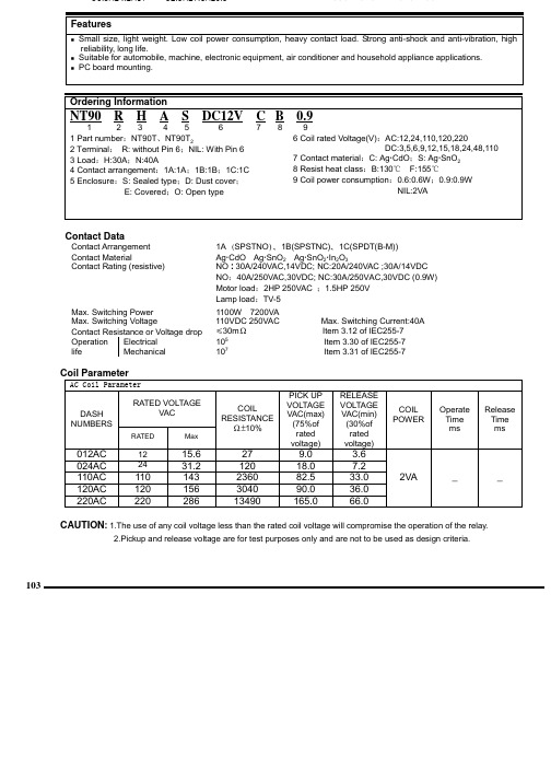
FeaturesSmall size, light weight. Low coil power consumption, heavy contact load. Strong anti-shock and anti-vibration, high reliability, long life.Suitable for automobile, machine, electronic equipment, air conditioner and household appliance applications.PC board mounting.Ordering InformationNT90 R H A S DC12V C B 0.91 2 3 4 5 6 7 8 91 Part number :NT90T 、NT90T 22 Terminal : R: without Pin 6;NIL: With Pin 63 Load :H:30A ;N:40A4 Contact arrangement :1A:1A ;1B:1B ;1C:1C5 Enclosure :S: Sealed type ;D: Dust cover ;E: Covered ;O: Open type6 Coil rated Voltage(V):AC:12,24,110,120,220DC:3,5,6,9,12,15,18,24,48,1107 Contact material :C: Ag CdO ;S: Ag SnO 28 Resist heat class :B:130℃ F:155℃9 Coil power consumption :0.6:0.6W ;0.9:0.9W NIL:2VA Contact DataContact Arrangement1A SPSTNO f 1B(SPSTNC)f 1C(SPDT(B-M))Contact MaterialAg CdO Ag SnO 2 Ag SnO 2 In 2O 3Contact Rating (resistive)NO : 30A/240VAC,14VDC; NC:20A/240VAC ;30A/14VDC NO :40A/250VAC,30VDC; NC:30A/250VAC,30VDC (0.9W)Motor load :2HP 250VAC ;1.5HP 250V Lamp load :TV-5Max. Switching Power1100W 7200VA Max. Switching Voltage110VDC 250VAC Max. Switching Current:40A Contact Resistance or Voltage drop አ30m Item 3.12 of IEC255-7Electrical 105Item 3.30 of IEC255-7Operation life Mechanical107Item 3.31 of IEC255-7Coil ParameterAC Coil ParameterRATED VOLTAGEVACDASH NUMBERSRATEDMaxCOIL RESISTANCE ±10%PICK UP VOLTAGE VAC(max)(75%of rated voltage)RELEASE VOLTAGE VAC(min)(30%of rated voltage)COIL POWEROperate Time ms Release Time ms012AC 1215.6279.0 3.6024AC 2431.212018.07.2110AC 110143236082.533.0120AC 120156304090.036.0220AC22028613490165.066.02VA __CAUTION : 1.The use of any coil voltage less than the rated coil voltage will compromise the operation of the relay.2.Pickup and release voltage are for test purposes only and are not to be used as design criteria.10330.5×24.2×17 32.5×27.6×20.5 99312549.2 01311661.4元器件交易网003-9003 3.9102.250.3005-9005 6.5283.750.5006-90067.8404.500.6009-900911.790 6.750.9012-9001215.61609.00 1.2015-9001519.525010.25 1.5018-9001823.436013.50 1.8024-9002431.264018.00 2.4048-9004862.4256036.00 4.8110-9001101431344582.5011.00.91510003-6003 3.915 2.250.3005-6005 6.542 3.750.5006-60067.860 4.500.6009-600911.7135 6.750.9012-6001215.62409.00 1.2015-6001519.537510.25 1.5018-6001823.454013.50 1.8024-6002431.296018.00 2.4048-6004862.4384036.00 4.8110-6001101432016782.5011.00.61510CAUTION : 1.The use of any coil voltage less than the rated coil voltage will compromise the operation of the relay.2.Pickup and release voltage are for test purposes only and are not to be used as design criteria.Qualification inspection:Perform the qualification test as specified in the table of IEC255-19-1 and minimum sample size 24.Operation conditionInsulation Resistance 1000M min (at 500VDC)Item 7 of IEC255-5Dielectric Strength Between contactsBetween contact and coil 50Hz 1500V 50Hz 2500V 4000V without Pin 6 Item 6 of IEC255-5Item 6 of IEC255-5Shock resistance 200m/s 2 11msIEC68-2-27 Test Ea Vibration resistance 10~55Hz double amplitude 1.5mm IEC68-2-6 Test Fc Terminals strength 10NIEC68-2-21 Test Ua1Solderability235 x 2 3x 0.5s IEC68-2-20 Test Ta method 1Ambient Temperature -55~100 -55~125 Relative Humidity 85% (at 40 )IEC68-2-3 Test CaMass27g Open type 30g元器件交易网。
q100电源芯片引脚功能参数
q100电源芯片引脚功能参数
Q100电源芯片是一种具有高效率和低功耗的集成电路,用于
电源管理和电源转换的应用。
它的引脚功能参数包括:
1. Vin:输入电压引脚,用于连接电源输入。
2. GND:接地引脚,用于连接电源的地。
3. Vout:输出电压引脚,用于连接电源芯片的电源输出。
4. EN:使能引脚,用于控制电源芯片的工作状态,通常通过
给EN引脚提供高电平来使能电源芯片。
5. FB:反馈引脚,用于调整输出电压。
通常通过与电压分压
电阻网络相连,将一定比例的输出电压反馈给芯片,以实现对输出电压的调节。
6. PG:输出电压监测引脚,用于检测输出电压的情况。
通常
通过给PG引脚提供一个电平,表示输出电压稳定或者异常。
7. SS:软起动引脚,用于控制电源芯片的软起动时间。
通常
通过给SS引脚提供一个时间常数来设置软起动时间。
8. BST:上电源引脚,用于连接输入电容。
通常通过给BST
引脚提供电压来为电源芯片提供额外的电源支持。
这些参数可以根据具体的电源芯片型号和应用需求来有所不同,
以上只是一些常见的功能参数。
在使用Q100电源芯片时,应参考数据手册中的详细说明和推荐应用电路设计。
海德汉数控系统组成

主计算机MC, 控制计算机CC, 硬盘HDR, SIK
CC 424
抽屉式硬盘
3
MC 422B
显示器BF, 键盘TE, 机床操作面板MB
BF 150
MB 420
TE 420
4
电源模块UV, 功率轴电机 QAN
6
手轮 HR
HR 410 HR 420
7
测头TS, TT
11
软件介绍 TNCopt
12
软件介绍 PLCdesignNT
13
系统集成
380V ~
UV1xx UM 1xxD CC4xx MC422B
TNC软件
14
TS 220 / TS 640 工件对齐和测量
TT 130 刀具静止或运动时测量
8
PLC 模块
PL 510 基本模块 IO Module PLD 16-8 Analog Module PLA 4-4
PL 510 with 4 I/O Modules PLD 16-8
PL 510 partially assembled
2
6 1
8
8
4
1 1
3
7
1
TNC 各功能部件名称及功能简介
主计算机 MC 、控制计算机 CC、硬盘HDR 、系统软件识别卡 SIK 显示器 BF、键盘 TE、操作面板 MB 电源模块 UV、功率模块UM 进给轴电机 QSY、主轴电机QAN 手轮 HR, 工件测头TS,刀具测头TT PLC基板 PL、 PLC I/O扩展模块 PLD 电抗器 KDR、线路滤波器EPCOS、制动电阻UP 110 软件: TNCopt, TNCdiag, TNCscopeNT, PLCdesignNT, TNCremoNT, TeleService, LSV2 tool…
热电偶冷端补偿芯片型号
热电偶冷端补偿芯片型号
热电偶冷端补偿芯片是用于测量和补偿热电偶在温度测量过程中由于冷端温度变化而产生的误差的一种电子元件。
这些芯片通常具有高精度、低温漂移和快速的响应时间。
冷端补偿是必要的,因为热电偶的热电势与热电偶两端的温度差有关,而温度的测量又涉及到冷端温度的影响。
以下是一些常见的热电偶冷端补偿芯片型号:
1. Maxim Integrated MAX1232:这是一个微处理器监控芯片,提供热电偶温度测量和冷端补偿功能。
2. Texas Instruments TMP006/TMP007:这些是用于摄氏温度测量和冷端补偿的数字温度传感器。
3. Analog Devices AD590:这是一个用于温度测量和冷端补偿的电流输出型温度传感器。
4. Broadcom BCP165/BCP166:这些是带有冷端补偿功能的温度传感器。
5. STMicroelectronics STM706/STM706P/STM706M:这些是带有集成冷端补偿的温度监控芯片。
6. On Semiconductor NCP188/189:这些是用于温度测量和冷端补偿的监控芯片。
需要注意的是,选择合适的热电偶冷端补偿芯片时,需要考虑应用的特定要求,例如温度范围、精度、输出类型(模拟或数字)、响应时间以及与其他系统的兼容性等因素。
在实际应用中,可能还需要
根据热电偶的类型和工作条件来调整补偿参数。
因此,在购买和使用之前,建议详细查阅芯片的技术规格和数据手册,以确保它们满足您的应用需求。
Honeywell HC900 操作员接口说明书
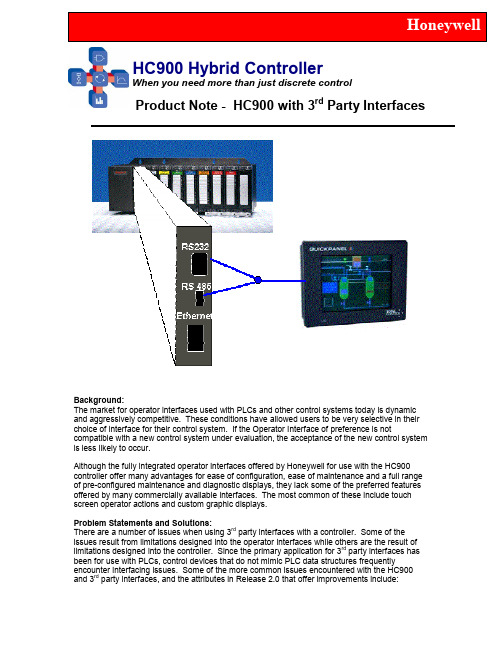
2. Some operator interfaces support the Modbus RTU protocol used in the HC900, but only support “holding register” data addresses up to 4096 or 32,000 (decimal). Note that the listed address range for a touch panel’s Modbus RTU driver may include a leading 4 or 3 in the address range number and it may be 5 or 6 digit. In this case, the first digit really refers to the Modbus “function code”. For example, as shown below, a Maple Systems panel has a range of 4096 (not 44096) for “Holding/Output Registers”, so it would not cover the range needed for the HC900.
Release 2: This requirement has not been impacted by changes in release 2 and remains an important selection criterion when choosing an operator interface to work with the HC900 controller.
MC9S08AC16数据手册(中文)

苏州大学飞思卡尔嵌入式系统研发中心翻译 2009 年 11 月
1
MC9S08AC16 系列特点
MC9S08AC16 系列特点
z 消费&工业 MC9S08AC16 MC9S08AC8
z 汽车 MC9S08AW16A MC9S08AW8A
3.6.1 Stop2 模式................................................................................................................................. 23 3.6.2 Stop3 模式................................................................................................................................. 23 3.6.3 停止模式下激活 BDM 使能 ................................................................................................... 24 3.6.4 停止模式下 LVD 使能 ............................................................................................................ 24 3.6.5 停止模式下的片上外设模块 .................................................................................................. 24
hc900综合控制器技术概述说明书
hc900综合控制器技术概述说明书HC900综合控制器是一种先进的工业自动化控制设备,它具有广泛的应用范围和可靠的性能。
本文将对HC900综合控制器的技术进行概述,介绍其主要特点和应用领域。
HC900综合控制器是霍尼韦尔公司推出的一款集控制、测量、调节和通信于一体的设备。
它采用了先进的控制算法和可编程逻辑控制器(PLC)技术,能够实现对工业过程的精确控制和监测。
同时,HC900综合控制器还具有高度可靠性和灵活性,能够适应各种复杂的工业环境和应用需求。
HC900综合控制器具有多种输入和输出接口,可以连接各种传感器和执行器,实现对不同参数的测量和调节。
它支持多种通信协议和网络接口,能够与其他设备进行数据交换和远程监控。
此外,HC900综合控制器还具有丰富的功能模块和编程接口,用户可以根据实际需求进行定制和扩展。
HC900综合控制器适用于各种工业自动化领域,如化工、石油、电力、制药等。
它可以应用于过程控制、温度控制、压力控制、液位控制等各种控制任务。
同时,HC900综合控制器还支持多种控制策略和算法,如PID控制、模糊控制、神经网络控制等,能够满足不同应用场景的需求。
HC900综合控制器具有可靠性高、操作简便、维护方便等优点。
它采用了先进的硬件和软件设计,具有强大的抗干扰和故障诊断能力,能够确保工业过程的稳定运行。
同时,HC900综合控制器还提供了友好的人机界面和操作界面,用户可以通过触摸屏或计算机进行参数设置和监控。
HC900综合控制器是一种功能强大、性能稳定的工业自动化控制设备。
它在各个行业的应用中取得了良好的效果,得到了广大用户的认可和赞赏。
随着工业自动化的不断发展,HC900综合控制器将继续发挥其独特的优势,为工业生产提供更加可靠和高效的控制解决方案。
NTE1900资料
NTE1900Integrated Circuit3–Terminal Adjustable PositiveVoltage RegulatorDescription:The NTE1900 is an adjustable 3–terminal positive voltage regulator in a TO92 type package capable of supplying in excess of 100mA over a 1.2V to 37V output range. This device is exceptionally easy to use and both line and load regulation are better than standard fixed regulators.In addition to higher performance than fixed regulators, the NTE1900 offers full overload protection available only in IC’s. Included on the chip are current limit, thermal overload protection, and safe area protection. All overload protection circuitry remains fully functional even if the adjustment termi-nal is disconnected.Normally, no capacitors are needed unless the device is situated far from the input filter capacitors in which case an input bypass is needed. An optional output capacitor can be added to improve tran-sient response. The adjustment terminal can be bypassed to achieve very high ripple rejection ratios which are difficult to achieve with standard 3–terminal regulators.Besides replacing fixed regulators, the NTE1900 is useful in a wide variety of other applications. Since the regulator is “floating” and sees only the input–to–output differential voltage, supplies of several hundred volts can be regulated as long as the maximum input to output differential is not exceeded. Also, it makes an especially simple adjustable switching regulator, a programmable output regulator, or by connecting a fixed resistor between the adjustment and output, the NTE1900 can be used as a precision current regulator. Supplies with electronic shutdown can be achieved by clamping the adjustment terminal to GND which programs the output to 1.2V where most loads draw little current.Features:D Adjustable Output Down to 1.2VD Guaranteed 100mA Output CurrentD Line Regulation Typically 0.01%/VD Load Regulation Typically 0.1%D Current Limit Constant with TemperatureD Eliminates the Need to Stock Many VoltagesD80dB Ripple RejectionAbsolute Maximum Ratings:Power Dissipation, P D Internally Limited . . . . . . . . . . . . . . . . . . . . . . . . . . . . . . . . . . . . . . . . . . . . . . . . . .. . . . . . . . . . . . . . . . . . . . . . . . . . . . . . . . . . . . . . . . . . . . . . . Input–Output Voltage Differential, V I–V O40V. . . . . . . . . . . . . . . . . . . . . . . . . . . . . . . . . .Operating Junction Temperature Range, T J–40° to +125°C. . . . . . . . . . . . . . . . . . . . . . . . . . . . . . . . . . . . . . . . . .Storage Temperature Range, T stg–65° to +150°C. . . . . . . . . . . . . . . . . . . . . . . . . . . . . . . . . . . .Lead Temperature (During Soldering, 10sec), T L+300°CElectrical Characteristics:(–25° ≤ T J ≤ +125°C, V IN –V OUT = 5V, I O = 40mA, I MAX = 100mA,Note 1 unless otherwise specified)Note 1.Although power dissipation is internally limited, these specifications are applicable for powerdissipations of 625mW.Note 2.Regulation is measured at constant junction temperature, using pulse testing with a low dutycycle. Changes in output voltage due to heating effects are covered under the specification for thermal regulation.Note 3.Thermal resistance is 180°C/W junction to ambient with 0.4” leads from a PC board and。
- 1、下载文档前请自行甄别文档内容的完整性,平台不提供额外的编辑、内容补充、找答案等附加服务。
- 2、"仅部分预览"的文档,不可在线预览部分如存在完整性等问题,可反馈申请退款(可完整预览的文档不适用该条件!)。
- 3、如文档侵犯您的权益,请联系客服反馈,我们会尽快为您处理(人工客服工作时间:9:00-18:30)。
Features
n
Small size, light weight. Low coil power consumption, heavy contact load. Strong anti-shock and anti-vibration, high
reliability, long life.
n
Suitable for automobile, machine, electronic equipment, air conditioner and household appliance applications.
Contact Data
Contact Arrangement 1A, 1B, 1C
Contact Material
Ag CdO Ag SnO 2 Ag SnO 2 In 2O 3
Contact Rating (resistive)
NO :30A/240VAC,14VDC; NC:20A/240VAC ;30A/14VDC NO;40A/250VAC,28VDC; NC:30A/250VAC,28VDC (0.9W)Max. Switching Power 1100W 7200VA
Max. Switching Voltage
110VDC 250VAC Max. Switching Current:40A Contact Resistance or Voltage drop 30m Ω Max Item 3.12 of IEC255-7Electrical 105 Item 3.30 of IEC255-7Operation life Mechanical
107 Item 3.31 of IEC255-7
Coil Parameter
DC Coil Parameter
AC Coil Parameter Coil voltage VDC
Coil resistance Ω±10%
Pick up voltageE VDC(max)(75%of rated voltage)Release voltage VDC(min)(10%of rated voltage)Coil power W
Operate Time ms Max
Release Time ms Max
Rated voltage VAC
Coil resistance Ω±10%
Coil
power
Rated Max
3 3.910/15 2.250.312(27)5 6.528/42 3.750.567.840/60 4.500.624
(120)911.790/135 6.750.91215.6160/2409.00 1.2110(2360)1519.5250/37510.25 1.51823.4360/54013.50 1.8120(3040)2431.2640/96018.00 2.44862.42560/384036.00 4.8220
(13490)
11014313445/20167
82.50
11.0
0.9/0.6
15
10
2VA
CAUTION : 1.The use of any coil voltage less than the rated coil voltage will compromise the operation of the relay.
2.Pickup and release voltage are for test purposes only and are not to be used as design criteria.
Operation condition
Insulation Resistance 1000M Ω min (at 500VDC)Item 7 of IEC255-5Dielectric Strength Between contacts
Between contact and coil 50Hz 1500V 50Hz 2500V
Item 6 of IEC255-5Item 6 of IEC255-5
Shock resistance 200m/s 2 11ms
IEC68-2-27 Test Ea method 1Vibration resistance 10~55Hz double amplitude 1.5mm IEC68-2-6 Test Fc Terminals strength 10N
IEC68-2-21 Test Ua1
Solderability
230 ºC ± 2 ºC 10± 0.5s IEC68-2-20 Test Ta method 1Ambient Temperature -55~100 ºC -55~125 ºC Relative Humidity 85% (at 40 ºC)IEC68-2-3Test Ca
Mass
37g
Qualification inspection: Perform the qualification test as specified in the table IV of IEC255-19-1 and minimum sample size 24.
79
N T 90T P (T 92)
LR956331
32.4(50)×27×28.5
元器件交易网。
