基于AD9851的信号发生器(带程序).
基于AD9851扫频信号发生器的设计
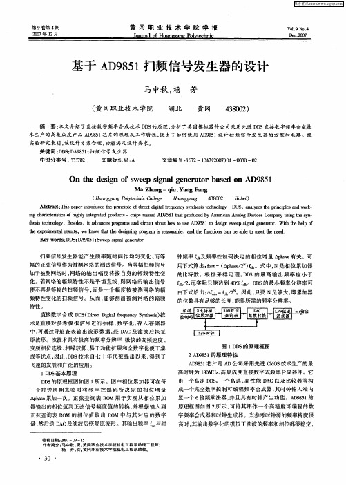
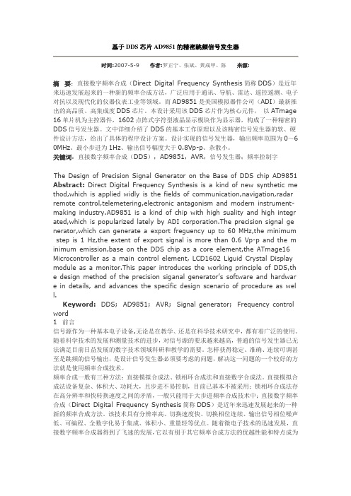
图 1D S的原理框 图 D
2A 95 的 原 理 特 性 D81
成等优点 , 因此 ,D 技术 自七 十年代 被提 出 以来 , 到 了 DS 得
飞速的发展 和广泛 的应用 。
1D S 本 原 理 D 基
A 95 芯片是 A D81 D公司采用先进 C O 技术生产的最 M S
teep r na eut,w n w ta ed s nn rga i aoa l,adtef f n a ea l e ene . h x ei t r. i me l s s ek o t h ei igporm r sn be n mc o sC b bet mett e d h t g se h i i n o h
术生产的高集成度产品 A 9 5 D 81芯片的原 ̄T - LX 作特 性 , 出 了如何使 用 A 95 设计扫 频信 号发生 器的方案和 电路 。经 提 D 81
实验研 究表明 , 该设计方案合理 , 功能满足设计要求 。
关 键 词 :D ; A 8 1扫 频 信 号 发 生 器 D SD 95 ;
中图分类号 : H 0 T7 2
文献标识码 : A
文章编号 :62 O7 2c )4 00— 2 17 —14(0r o —03 0 7
O n t e in o we p sg a e r t rba e n AD 9 5 he d sg fs e in lg ne a o s d o 81
M a Zh n o g—q u, n n i Ya g Fa g
( u ng n o t hi C lg H ag agP l e n oee yc c l
t a g ag l ng n u
480 302
H bi ue)
(完整word版)基于AD9851的信号发生器(带程序)
基于AD9851的信号发生器最近几年的电子设计大赛,差不多每年都考了DDS的设计。
本人曾经也调试过DDS,但走了一些弯路,在这里写下一些心得,希望能对初调者有点帮助。
下面将有电路图,以及详细的代码。
学过FPGA的同仁们,应该对DDS的原理就会有很好的理解了。
用FPGA是很容易把一个简单型的ad8952烧出来的!其实原理相当的简单,无非就是由相位累加器,相位调制器,正弦查找ROM,DAC构成。
通过改变相位累加的增量就很容易的改变的输出的频率了。
如果相位累加器(频率控制子)的位宽为N位(ad9851的N=32位)这就意味着把一个周期的正弦波形离散成了2的N次方个点,把这些点的幅值存在一个ROM中就构成了正弦查找ROM。
如果系统时钟为Fclk,即把Fclk分成了2的N 次方份。
如果此时的相位累加增量为(频率控制字)为B,那么此时的输出频率应为Fout=(B*Fclk)/ N。
显然B=1时其最小值为Fclk/ N。
B的值也不能太大,否则会输出失真波形。
Fout的最大值理论上应该至少小于Fclk/4。
所以要想提高输出频率的最大值,就得靠提高系统的外部时钟Fclk。
下面结合本人的代码来具体讲讲AD9851的应用。
AD9851的一些具体介绍这里就不说了。
其DATASHEET上都说的很清楚。
若看不懂E文,可以发E_M给我,我有中文资料。
AD9851要写40位的控制子。
其中前面32位就是频率控制子了。
后面是有1个6倍频使能位,1个logic0位,1个POWER_DOWN位,还有5位相位模式字。
这里我们只解决频率控制问题。
也就是说在代码中本人只写了,32位的频率控制子,还有一个6倍频使能。
其余的剩下几位由于没用到也就默认写为0了。
AD9851可以用并和串俩中方式写入控制子。
其串行发送方式的控制子表如下:本人主要将用串写控制子的时序与代码。
其并的方式的代码也会给出。
硬件电路图网上有很多资源,自己去找找!主要看看代码吧:/*************************************************************ad9851串口驱动程序2007-8-28-------------water************************************************************/#include <reg52.h>#include <intrins.h>#include <ABSACC.H>//-----------------------定义管脚--------------------------------------------------------sbit D7=P3^3; //控制子串传送位sbit DDS_FQUD=P3^4; //更新发送频率sbit DDS_CLK=P3^5; //接外部晶振时钟这里为30Munsigned long control_word(float freq);void send_control( unsigned long bytedata);void AD9851Init(void) //DDS初始化函数,包括DDS复位和初始化为串行发送{DDS_CLK=0;DDS_FQUD=0;DDS_CLK=1;DDS_CLK=0;DDS_FQUD=1;DDS_FQUD=0;}main(){unsigned long x;DDS_FQUD=0;AD9851Init();x=control_word(500000);while(1)send_control(x);}//计算9851控制字,freq为你要输出的频率unsigned long control_word(float freq){unsigned long water;water=23.86115*freq;//外部晶振为30M,6倍频后180M,其关系由公式算出。
AD9851程序及说明

clk=0;//CLK置低
for(i=0;i<5;i++)//送入5个字节的控制字
{
temp=ww[i];
for(j=0;j<8;j++)
{
clk=0;
if(temp&0x01)dat=1;
else dat=0;
delay_us(2);
clk=1;
delay_us(2);
#definerst2
#define dat3
unsignedchar phase_word=0x00;//相位控制字,使用低5位
unsigned char power_down=0x00;//低功耗模式
unsigned char mult=0x01;//6倍频是否打开
unsigned char ww[5]={0x09,0x0E,0x38,0xE3,0x8E};
void write_dds(unsigned long dds)
{
unsigned chari,j,temp;
ww[0]=dds&0xFF;//频率字最低字节
ww[1]=(dds>>8)&0xFF;
ww[2]=(dds>>16)&0xFF;
ww[3]=dds>>24;//频率字最高字节
ww[4]=(phase_word<<3)|| power_down<<2 || mult;//控制字
unsigned char ww[5]={0x09,0x0E,0x38,0xE3,0x8E};
unsigned long freq,set_value;
基于AD9851信号发生器的设计
基于AD9851信号发生器的设计摘要:基于直接数字频率合成(DDS)原理,采用AD9851型DDS器件设计一个信号发生器,实现50 Hz~60 MHz范围内的正弦波输出。
通过功率放大,在50Ω负载的情况下,该信号发生器在50 Hz~10 MHz范围内输出稳定正弦波,电压峰峰值为0~5V±0.3V。
关键词:DDS;直接数字频率合成;AD9851;微处理器;C语言0 引言直接数字合成(DDS)是近年来新的电子技术。
单片集成的DDS产品是一种可代替锁相环的快速频率合成器件。
DDS是产生高精度、快速变换频率、输出波形失真小的优先选用技术。
DDS以稳定度高的参考时钟为参考源,通过精密的相位累加器和数字信号处理,通过高速D/A 变换器产生所需的数字波形(通常是正弦波形),这个数字波经过一个模拟滤波器后,得到最终的模拟信号波形。
DDS系统一个显著的特点就是在数字处理器的控制下能够精确而快速地处理频率和相位。
除此之外,DDS的固有特性还包括:相当好的频率和相位分辨率(频率的可控范围达μHz级,相位控制小于0.09°),能够进行快速的信号变换(输出DAC的转换速率百万次/秒)。
1 AD9851集成芯片简介AD9851相对于AD9850的内部结构,只是多了一个6倍参考时钟倍乘器,当系统时钟为180MHz时,在参考时钟输入端,只需输入30 MHz的参考时钟即可。
AD9851是由数据输入寄存器、频率/相位寄存器、具有6倍参考时钟倍乘器的DDS芯片、10位的模/数转换器、内部高速比较器这几个部分组成。
其中具有6倍参考时钟倍乘器的DDS芯片是由32位相位累加器、正弦函数功能查找表、D/A变换器以及低通滤波器集成到一起。
这个高速DDS芯片时钟频率可达180MHz,输出频率可达70 MHz,分辨率为0.04Hz。
AD9851可以产生一个频谱纯净、频率和相位都可编程控制且稳定性很好的模拟正弦波,这个正弦波能够直接作为基准信号源,或通过其内部高速比较器转换成标准方波输出,作为灵敏时钟发生器来使用。
一种基于AD9851芯片的DDS脉冲发生器
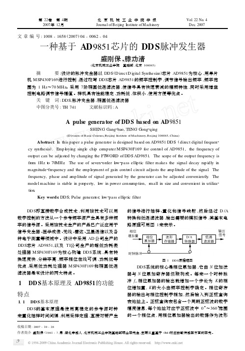
第22卷 第4期2007年12月 北京机械工业学院学报Journal of Beijing I nstitute ofM achinery Vol .22No .4Dec .2007文章编号:1008-1658(2007)04-0062-04一种基于AD 9851芯片的DD S 脉冲发生器盛刚保,滕功清(北京机械工业学院 基础部,北京100085)摘 要:设计的脉冲发生器以DDS (D irect D igital Synthesize )芯片AD9851为核心,用单片机MSP430F169进行控制,通过改写DDS 芯片AD9851的频率控制字,调节信号输出频率,频率范围为1Hz ~70MHz 。
采用7阶椭圆低通滤波器,使信号具有快速衰减的幅频特性,同时采用增益控制电路调节信号幅值。
样机具有性能稳定,功耗低,体积小,使用方便等优点。
关 键 词:DDS;脉冲发生器;椭圆低通滤波器中图分类号:TH 741 文献标识码:AA pulse genera tor of DD S ba sed on AD 9851SHE NG Gang 2bao,TENG Gong 2qing(D ivisi on of Basic Courses,Beijing I nstitute of Machinery,Beijing 100085,China )Abstract :I n this paper a pulse generat or is designed based on AD9851DDS (direct digital frequen 2cy synthesis ).E mp l oying single chi p co mputer MSP430F169for contr ol of AD9851,the frequency of out put can be adjusted by changing the FT WORD of DDS AD9851.The scope of the out put frequency is fr om 1Hz t o 70MHz .The use of seven 2order l ow 2pass elli p tic filter makes the signal decay rap idly in magnitude 2frequency and the e mp l oy ment of gain contr ol circuit adjusts the a mp litude of the signal .The frequency,phase and a mp litude of signal generated by the generat or can be adjusted conveniently .The model machine is stable in p r operty,l ow in power consu mp ti on,s mall in size and convenient in utiliza 2ti on .Key words :DDS;Pulse generat or;l ow 2pass elli p tic filter DDS 即直接数字合成技术,利用该技术可以用数字控制的方法从一个参考频率源产生具有多种频率的信号源。
AD9851 程序1
}
//写w1数据
w=(y>>24);
for(i=0;i<8;i++)
{
ad9851_bit_data=(w>>i)&0x01;
ad9851_w_clk=1;
ad9851_w_clk=0;
}
//写w0数据
w=w0;
for(i=0;i<8;i++)
sbit ad9851_rest =P2^0; //P2.0口接AD9851的rest脚/PIN12
sbit ad9851_bit_data =P1^7; //P1.7口接AD9851的D7脚/PIN25
//P1为8位数据口
//***************************************************//
//函数3: ad9851_wr_parrel(unsigned char w0,double frequence)
// 并口写ad9851数据,w0为ad9851中w0的数据,frequence
// 为写入的频率
//函数4: ad9851_wr_serial(unsigned char w0,double frequence)
// 向ad9851中写命令与数据(串口) //
//---------------------------------------------------//
void ad9851_wr_serial(unsigned char w0,double frequence)
//函数4: ad9851_wr_serial(unsigned char w0,double frequence)//
AD9851制作的信号发生器.
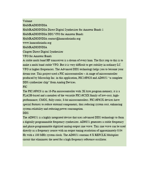
VolumeHAMRADIOINDIAHAMRADIOINDIA Direct Digital Synthesizer for Amateur Bands 1 HAMRADIOINDIA DDS VFO for Amateur BandsHAMRADIOINDIA contact@HAMRADIOINDIAChapter Direct Digital SynthesizerVFO for Amateur BandsA stable multi band HF transceiver is a dream of every ham. The first step to this is to make a multi band stable VFO. But it is very difficult to get stability in ordinary LC VFO at higher frequencies. The Advanced DDS technology helps you to become your dream true. This project used a PIC microcontroller – A range of microcontroller produced by Microchip Inc. in this application, PIC16F628 and AD9851 “a complete DDS synthesizer chip” from Analog Devices.PICThe PIC16F628 is an 18-Pin microcontroller with 2K byte program memory, it is a FLASH-based and a member of the versatile PIC16CXX family of low-cost, high-performance, CMOS, fully-static, 8-bit microcontrollers. PIC16F62X devices have special features to reduce external components, thus reducing system cost, enhancing system reliability and reducing power consumption.DDSThe AD9851 is a highly integrated device that uses advanced DDS technology to form a digitally programmable frequency synthesizer. AD9851 generates a stable frequency and phase-programmable digitized analog output sine wave. This sine wave can be used directly as a frequency source with an output tuning resolution of approximately 0.04 Hz with a 180 MHz system clock. The AD9851 contains 6 X REFCLK Multiplier circuit that eliminates the need for a high frequency reference oscillator.Figure 1. Basic DDS Block Diagram2HAMRADIOINDIAThe basic block diagram is shown in Figure 1. The frequency out put can be calculated using the following formulaeFout = (∆ Phase X Syst em Clock)/ 2 ^ 32Where:∆ Phase = decimal value of 32 bit tuning wordSystem Clock = REFCLK frequency in MHz or 6 X REFCLK frequency(in MHz) if the 6 X REFCLK Multiplier is enabledFout = Output frequency of DDS in MHzThe DDS circuitry is basically a digital frequency divider function whose incremental resolution is determined by the frequency of the system clock, and N (number of bits in the tuning word). The phase accumulator is a variable-modulus counter that increments the number stored in it each time it receives a clock pulse. When the counter reachesfull-scale it wraps around, making the phase accumulator’s output phase-continuous. The frequency tuning word sets the modulus of the counter, which effectively determines the size of the increment (∆P hase) that will be added to the value in the phase accumulator on the next clock pulse. The larger the added increment, the faster the accumulator wraps around, which results in a higher output frequency.Figure 2. Output Spectrum of DDSIn the example shown in Figure 2, the system clock is 100 MHz and the output frequency set to 20 MHz. A low pass filter is essential to remove unwanted images. A good rule-of-thumb is limiting the output frequency to 1/3rd of System Clock frequency. One can use the other images also with help of a good band pass filter. Note that these images are not harmonics and it keeps a 1:1 relation with the fundamental frequency, i.e. if fundamental frequency increased 1 Hz then the image frequency also shifted 1 Hz.3HAMRADIOINDIAOperational Features1. Dual VFO, i.e. VFO A and VFO B facilities.2. Up to 20 RX frequency storage on memory3. The Software allows 2 modes of operation,a. VFO modeb. Memory mode4. Keypad frequency entry5. Step size can be changed from 1Hz to MHz range.6. RIT facility.7. Save to any MEM and copy to any VFO from MEM is possible.8. LSB/USB/CW modes9. Allows -Ve and +Ve IF OFFESTS10. Calibration screen for changing all the setup screens including Chiptype and System Clock Frequency.11. Signal Generator mode.12. Time out function for ignoring any wrong entry13. Low cost mechanical encoder is used14. A 2 x 16 line LCD display used for display freq and other messages Construction notes.The opto-coupler 4N35 is isolating the PTT from the circuit. To change frequency of the DDS, Keypad and Mechanical Rotary encoder are provided. Another six push button switches are used for managing other functions of the VFO. An ordinary keypad used in telephones, which is easily available from the local market is used. If the Mechanical encoder is not available one can use the encoder found in the “Scroll Mouse”. The scroll mouse contains two optical sensors and one mechanical encoder inside it. You can easily remove the mechanical encoder from the mouse and fit it to the front panel of your radio.DDS Chip AD9851BRS/AD9850BRS comes with SSOP package, it is somewhat difficult to solder for a home brewer. Seek the help of a service people to solder this chip to board is an alternative. May be one can try the method Peter Rhodes, G3XJP, in his article AN557 (). He solders this chip to a 24DIP socket using a short wire leads. But this method is not supported by the PCB design shown here. Or one can contact the local mobile phone servicing people to get the chip soldered to PCB.4HAMRADIOINDIAFigure 3. Dimensions of AD9851BRSA 2 line x 16 LCD with or without R/W pin (software use delays rather than busy checks) is used to display VFO frequency and other messages. The LCD contrast can be adjusted using R7 (10K pot). Commonly available LCD display (using HitachiHD44780 controller) is used in this circuitAfter assembling double check all wiring and check for any dry solder,loose connections etc. PCB may be cleaned with isopropyl. Note that higher than 5 V will damage both DDS and PIC chips. Always use a good IC socket for the PIC16F628, this will helps if you need to re-program the chip.The MODE SELECT output (from 74LS139) are used to switch crystalsand other operations while changing the modes (i.e. CW/LSB/USB etc.). One of the out put will be low and all other are high of 74LS139. one of the Band select out put will be low in the following conditions.1. Frequency less than 10 MHz – used for selecting 40 M2. Frequency less than 17 MHz – used for selecting 20 M3. Frequency less than 25 MHz – used for selecting 15 M4. Frequency greater than 25 MHz – used for selecting 10 MFigure 4. LCD display on TX mode.5HAMRADIOINDIACalibration and setup screensBy pressing down the CAL button for one second, you can enter thecalibration screen; here you can change the followings.1. Enable 6 X REFCLK Enable or Disable internal multiplier2. DDS_SYSTEM_CLK. Range 30 MHz to 190 MHz for AD98513. MAX_DDS_FREQ. Range 0MHz o 45% of DDS_SYSTEM_CLK4. MIN_RX_DDS_FREQ >= Max RIT Freq +Tx Offset frequency5. MAX_RX_DDS_FREQ <= MAX_DDS_FREQ –(Max_RIT_frequency +Tx_Offset_frequency6. MAX_RIT_FREQ7. SSB_OFFSET -/+ 1500 KHz8. CW_OFFSET -/+ 750Hz9. TX_OFFSET_FREQ Offset from RX Frequency10. OFFSET_FREQ IF Offset Added to TX/RX frequency11. MULTIPLIER Frequency display is multiplied by NTo Change the Setup screen press and hold the CAL button then power onthe VFO. After the version number display, the first calibration screen – Enable 6 X REFCLK is displayed. Use the rotary encoder to make the selection, and then briefly press the CAL button to go to the next screen. The first three calibration screens rarely need change. So you can change the rest all settings even when the DDS is working. To do this press and hold the CAL button for one second you will get the calibration screen. RX_DDS_FREQ, MIN_RX_DDS_FREQ, MAX_RX_DDS_FREQ,SSB_OFFSET, CW_OFFSET, TX_OFFSET_FREQ and OFFSET_FREQ are may be positive or negative values.The DDS system clock (DDS_SYSTEM_CLK), is the crystal frequencyor 6 x crystal frequency if 6XREFCLK multiplier enabled. This screen sets DDS output frequency to 10MHz and displays the DDS system clock frequency. Adjust the DDS system clock (Rotary encoder or keypad can be used) to get exactly 10 MHz out put from DDS. This screen continues to display until CAL button pressed briefly (here no timeout function).The Maximum DDS frequency (MAX_DDS_FREQ) is the limit of yourDDS Frequency and you can set a maximum value of system clock x 0.45, set this value to 1/3rd of your system clock or the cut of frequency on the low pass filter in the output which is the lowest.Minimum RX and Maximum RX frequency are the minimum andmaximum frequency limits of the VFO. Maximum RIT is the limit of RIT and you can set this is to a maximum up to 10MHz.SSB offset added to the out put frequency if the VFO is in USB mode orsubtract in LSB mode. The range is -30MHz to + 30MHz note that –ve offset just change the meaning of LSB and USB.i.e. If the SSB OFFSET is set to 1500 ( for a 3000 KHz filter bandwidth )LSB subtracts 1500 Hz from the DDS frequency,USB adds 1500 Hz to the DDS frequency.6HAMRADIOINDIAIf the SSB OFFSET is set to -1500LSB adds 1500 Hz to the DDS frequency,USB subtracts 1500 Hz from the DDS frequencyCW offset added to the VFO out put frequency if the VFO in RX modeand on TX SSB offset will be added. This will help you to use USB crystal to receive and transmit CW.TX offset add only when transmitting, and offset frequency adds inboth RX and TX. 20GHz is the maximum limit of the offset frequency.Frequency display is multiplied with the value MULTIPLIER. Therange of this value is from 1 to 1024, this will be useful if the VFO using in VHF or higher frequencies.Enter a valid frequency in all calibration screens, for an example RXmaximum frequency sets to a value, when added to other offsets (Offset frequency and SSB offsets etc.) result never cross the limit of Max DDS Frequency. If the all buttons and rotary encoder kept idle for 10 sec in any of the above set up screens except the REFCLK, all changes made are discarded and return to VFO screen. If any changes are made in any of the above screens, the message “SAVING” will be displayed at the end of CALL screen and return to VFO screen.Operational useOn power up the software version number is displayed for a short time. The second digit after decimal point will be 6 if you enabled the 6 XREFCLK, or it will be 1, if you are not using the same. For ease of operation Keypad, rotary encoder and other six buttons are provided. You can directly enter any value within the DDS limits. The “* “key represent the decimal point and “# “used to “enter” the value. For an example if you wants to enter 7.5 MHz, first press 7, the “* “key then 5 followed by “#” – th e “Enter key “. The frequency will be displayed as “7.500000 MHz”. When pressing any key in the keypad the same will be displayed in the LCD and the “MHz” text in the LCD has been change to “#” as a reminder to “#” key must be used after the frequency type d in. Press “#” key first to enter a –ve value, only allowed in some setup screens.Turn the rotary encoder clockwise increases the frequency and anti-clockwise decreases it. While pressing down the STEP button a cursor is displayed under one digit. This indicates the selected step size, and to change the same turn the rotary encoder while pressing down the STEP button. You can select step size from 1 Hz to 10MHz range. The software also monitor how fast you turn the knob, if you turn fast the frequency will be increasing a value higher than 1 and up to 30. Due to the software takes 4mS to de-bounce the encode position; if you turn so fast then no change will occur.Any changes in the frequency will write into the EEPROM two secondsafter stopping the rotary encoder or entering frequency by Keypad. On power up last the frequency stored in the EEPROM will be displayed.7HAMRADIOINDIAManaging two VFOsA VFO button is used to swaps over two VFOs, ie VFO A and VFO B.Both frequency and modes (i.e. CW/LSB/USB) associated with the VFO are swapped over with a brief press of VFO button. “VFOA” or “VFOB” is displayed in the LCD. SplitPressing down VFO button for 1 second will activate SPLIT mode. In this mode VFO will change from one to another on pressing the PTT and backwhen releasing it. A “SPT” will be displayed on LCD to indicate you are in SPLIT mode. RIT will be disabled in this mode.RITIf the RIT button is pressed briefly, RIT is displayed on the LCD andactivate RIT mode. The TX frequency cannot be changed, but the RX frequency can be changed as long as it does not cross the limits i.e. RX freq +/- maximum RIT offset. Pressing the RIT button again, removes the RIT display and the RX frequency reverts to its previous value.CW/LSB/USBPressing SSB button briefly change the mode one by one. No offset, CW, LSB, USB can be selected one by one. In CW mode CW offset willbe added if the VFO in the RX mode and SSB offset will be add if the VFO in TX mode. So you can use USB crystal to receive and transmit CW. In LSB mode SSB offset subtract from the output frequency and add in USB mode. The –ve offset justchanges the meaning of LSB and USB (see calibration and setup screens for more details). The CW, LSB, or USB displayed on LCD if anyone of these modes is selected. Memory FunctionMemory function has been used to save and recall RX frequencies toEEPROM. Max 20 numbers of frequencies can be saved. A brief press of memory button will change from VFO mode to Memory mode and back. On pressing memory button MEM 1 will be displayed, and you can select the desired memory with the rotary encoder. If the memory frequency is invalid a “---“will be displayed instead of MEM in the LCD. This happens when you change something in setup screens and try to recall old memory locations. For example if you change max RX freq to 30MHz and select a memory locations stored 40MHz.To save a VFO frequency in to memory, press MEM buttons for 1 sec,then select memory location using rotary encoder. To avoid erasing any useful frequency the frequency in that location will be displayed on the second line of LCD. Press MEM button after selecting the desired location for 1 sec. A message “SAVE” will be displayed on LCD. If you didn’t like to8HAMRADIOINDIAoverwrite the previous memory Frequencies then a brief press of MEM button helps to back to VFO mode.There are two methods to go back VFO mode from memory mode. Abrief press change to VFO mode and recall the previous VFO frequency. If you press MEM button for 1 second then the memory frequency will be copied to VFO and change to VFO mode.AcknowledgementsI was able to finish the project help and encouragements given to me by VU2ITI (Prof. T.K. Mani), VU3WIJ (Shaji.P.B).Reference:1. AD9851 CMOS 180 MHz DDS/DAC Synthesizer Data Sheet2. AN557 ( Analog Devices )9HAMRADIOINDIAChapter Circuit diagrams10 10Page 1 of 2Page 2 of 2。
基于AD9851的多功能信号发生器设计

万方数据万方数据人机交互以及定时中断程序等几部分构成。
其中主监控程序的任务是识别按键、解释命令,并获得完成该命令的相应模块人口,引导信号发生器进入正常工作状态,协调各部分软件的工作;典型信号产生程序则由STC516RD根据用户输人的频率和相位要求.将计算出的频率控制字传送给AD9851.再由AD9851产生频率相位可控的信号;定时中断程序需要11D和他定时器同时工作,TD用来定时扫描键盘,rI’2则工作在16位自动重装载方式.用来定时2PSK、ASK、FSK以及扫频功能中的时间间隔的长短,以及模拟多路转换开关的切换。
图3所示是系统主监控程序.即系统主程序流程图。
图3主程序流程图信号发生器的工作模式可以通过主监控程序中变量state的值进行选择。
每种功能的实现则依赖于频率、相位、幅度以及时间间隔的设定。
并应综合考虑。
在数字调制方法中。
数字调制的载波是AD9851输出的正弦信号,其频率和幅度均可调,调制波通常是一系列由0和1交替出现的序列信号串。
信号发生器的工作模式通常有以下几种:(11单频模式单频模式是最为灵活的一种.当需要信号发生器输出一个频率固定的正弦波时.通常采用此10电手充嚣件主用2009.9舢.eC出I.cn模式。
(2)二进制移相键控模式(2PSK)该模块是用已调信号载波的00和180。
分别表示二进制数字基带信号的1和0。
系统需要产生l和0相互交替出现的调制信号。
(31二进制幅度键控模式(ASK)即用载波在二进制调制信号1或O的控制下通或断。
本系统中,信号发生器产生的1和0可由输出信号幅度的不同衰减值来区分。
(4)二进制移频键控模式(FSK)如果二进制基带信号的1对应于载波频率.^,o对应于载波频瓤。
那么系统中信号发生器产生的l和0,就可由输出信号频率的不同来区分。
输出频率的最大值可为20MHz。
(5)扫频模式扫频模式主要用于测量网络的幅频特性。
可用示波器直接显示被测二端口网络的频率特性曲线。
单片机控制DDSAD9851程序
这是采用AD9851和AT89S52做成的正弦信号发生器,最高频率为70Mhz左右,还要配合一块12864带中文字库的液晶显示器和一个4X4的键盘,就可以任意输入想要的频率了,以下是源代码:;经过严格测试,本程序运行良好;其中 LCD_0-7是LCD显示内容的缓存地址;48H,47H,46H,45H 是 DDS 的频率控制字的缓存地址,以上是从低位向高位排列;********************************************************************RS EQU P3.2RW EQU P3.3E EQU P3.4W_CLK EQU P3.5FQ_UD EQU P3.6COM EQU21HDAT EQU22HLCD_0EQU37HLCD_1EQU38HLCD_2EQU39HLCD_3EQU3AHLCD_4EQU3BHLCD_5EQU3CHLCD_6EQU3DHLCD_7EQU3EH;*********************************************以上是接口及内存地址定义MAIN: WORK:KEY:ORG0000HMOV SP,#60HAJMP MAINORG0010HACALL FRE_INLACALL SHOW_FREACALL DISPLCALL LCDTODDSACALL AD9851MOV P1,#0FHMOV A,P1; 采用线反转法编写的程序CJNE A,#0FH,KEYAAJMP KEYKEYA:ACALL DELAY10MSMOV A,P1ANL A,#0FHCJNE A,#0FH,KEYBAJMP KEYKEYB:CPL AMOV B,ACJNE A,#0F0H,KEYCAJMP KEYKEYC:MOV P1,#0F0HMOV A,P1CPL AANL A,BKEY1:CJNE A,#84H,KEYAJMP MENUMENU:ACALL LCD_INLMOV COM,#82HACALL WRIACALL DELAYMOV DPTR,#TAB_FRESETMOV R2,#8SHOW_SET:CLR AMOVC A,@A+DPTRMOV DAT,AACALL WRDACALL DELAYINC DPTRDJNZ R2,SHOW_SETACALL DISPMOV R0,#38HKEY_MENU:ACALL DISPMOV P1,#0FH; 这是在菜单下的键盘程序MOV A,P1CJNE A,#0FH,KEY_MENUAAJMP KEY_MENUKEY_MENUA:ACALL DELAY10MSMOV A,P1ANL A,#0FHCJNE A,#0FH,KEY_MENUBAJMP KEY_MENUKEY_MENUB:CPL AMOV B,ACJNE A,#0F0H,KEY_MENUCAJMP KEY_MENUKEY_MENUC:MOV P1,#0F0HMOV A,P1CPL AANL A,BMOV R1,AKEY_OP1:CJNE A,#84H,KEY_OP2ACALL DISPAJMP KEY_MENUKEY_OP2:CJNE A,#18H,KEY_EXITACALL DISPAJMP KEY_MENUKEY_EXIT:CJNE A,#88H,KEY_OP3JMP WORKKEY_OP3:CJNE A,#44H,KEY_RIGHTAJMP KEY_MENUKEY_RIGHT:CJNE A,#48H,KEY_LEFTCJNER0,#3EH,KEY_RIGHT_OKMOV R0,#37HAJMP KEY_MENUKEY_RIGHT_OK:INC R0AJMP KEY_MENUKEY_LEFT:CJNE A,#28H,KEY_1CJNER0,#37H,KEY_LEFT_OKMOV R0,#3EHAJMP KEY_MENUKEY_LEFT_OK:DECR0AJMP KEY_MENUKEY_1:CJNE A,#11H,KEY_2MOV@R0,#1AJMP KEY_MENUKEY_2:CJNE A,#21H,KEY_3MOV@R0,#2AJMP KEY_MENUKEY_3:CJNE A,#41H,KEY_4MOV@R0,#3AJMP KEY_MENUKEY_4:CJNE A,#81H,KEY_5MOV@R0,#4AJMP KEY_MENUKEY_5:CJNE A,#12H, KEY_6MOV@R0,#5AJMP KEY_MENUKEY_6:CJNE A,#22H,KEY_7MOV@R0,#6AJMP KEY_MENUKEY_7:CJNE A,#42H,KEY_8MOV@R0,#7AJMP KEY_MENUKEY_8:CJNE A,#82H,KEY_9MOV@R0,#8AJMP KEY_MENUKEY_9:CJNE A,#14H,KEY_0MOV@R0,#9AJMP KEY_MENUKEY_0:MOV@R0,#0AJMP KEY_MENU;*************************************************以上是键盘处理程序SHOW_FRE:ACALL LCD_INLMOV COM,#81HACALL WRIACALL DELAYMOV DPTR,#TAB_DDSMOV R0,#12SHOW_FRE1:CLR AMOVC A,@A+DPTRMOV DAT,AACALL WRDACALL DELAYINC DPTRDJNZ R0,SHOW_FRE1 SHOW_FRE2:MOV COM,#90HACALL WRIACALL DELAYMOV DPTR,#TAB_FRENOWMOV R0,#10SHOW_FRE3:CLR AMOVC A,@A+DPTRMOV DAT,AACALL WRDACALL DELAYINC DPTRDJNZ R0,SHOW_FRE3RETFRE_INL:MOV37H,#3MOV38H,#9MOV39H,#5MOV3AH,#0MOV3BH,#0MOV3CH,#0MOV3DH,#0MOV3EH,#0RETDISP:MOV COM,#89HACALL WRIACALL DELAYMOV A,37H ADD A,#30H MOV DAT,A ACALL WRD ACALL DELAY MOV A,38H ADD A,#30H MOV DAT,A ACALL WRD ACALL DELAY MOV DAT,#2EH ACALL WRD ACALL DELAY MOV A,39H ADD A,#30H MOV DAT,A ACALL WRD ACALL DELAY MOV A,3AH ADD A,#30H MOV DAT,A ACALL WRD ACALL DELAY MOV A,3BH ADD A,#30H MOV DAT,A ACALL WRD ACALL DELAY MOV A,3CH ADD A,#30H MOV DAT,A ACALL WRD ACALL DELAY MOV A,3DH ADD A,#30H MOV DAT,AACALL WRDACALL DELAYMOV A,3EHADD A,#30HMOV DAT,AACALL WRDACALL DELAYMOV DAT,#4DHACALL WRDACALL DELAYMOV DAT,#48HACALL WRDACALL DELAYMOV DAT,#7AHACALL WRDACALL DELAYRET;********************************************以上是显示频率子程序LCD_INL:MOV COM,#30HACALL WRILCALL DELAYMOV COM,#0CHACALL WRILCALL DELAYMOV COM,#01HACALL WRILCALL DELAYMOV COM,#06HACALL WRILCALL DELAYRET;***************************************以上是液晶显示器显示时间的初始化AD9851:ACALL AD9851_INLMOV R2,#05H; 写相位控制字MOV R1,#44H; 写频率控制字MOV44H,#01HSEND_WORD:MOV P2,@R1SETB W_CLKCLR W_CLKINC R1DJNZ R2,SEND_WORDSETB FQ_UDCLR FQ_UDRETAD9851_INL:MOV P2,#0CLR W_CLK;初始化信号脚CLR FQ_UDSETB W_CLKCLR W_CLKSETB FQ_UDCLR FQ_UDRETWRI:PUSH ACCPUSH DPLPUSH DPHCLR RSSETB RWWRI1:MOV P0,#0FFHSETB EMOV A,P0CLR EJB ACC.7,WRI1CLR RWMOV P0,COMSETB ECLR EPOP DPHPOP DPLPOP ACCRET;******************************************以上是写指令子程序WRD:PUSH ACCWRD1:PUSHPUSHCLRSETBMOVSETBMOVCLRJBSETBCLRMOVSETBCLRPOPPOPPOPRETDPLDPHRSRWP0,#0FFHEA,P0EACC.7,WRD1RSRWP0,DATEEDPHDPLACC;******************************************以上是写数据子程序DELAY:MOV R7,#0FFHDELAY4:MOV R6,#00FHLOOP2:DJNZ R6,LOOP2DJNZ R7,DELAY4RETDELAY10MS:PUSH00HPUSH01HMOV01H,#64HDELAYA :MOV00H,#0A0HDELAYB :DJNZ00H,DELAYBDJNZ01H,DELAYAPOP01HPOP00HRETDELAY1:MOV R4,#08HDELAY11:MOV R7,#0FFHDELAY41:MOV R6,#0FFHDJNZ R6,$DJNZ R7,DELAY41DJNZ R4,DELAY11RET;******************************************以上是延时子程序LCDTODDS:MOV48H,#0MOV47H,#0MOV46H,#0MOV45H,#0MOV R0,#48HCLR AMOV B,#0MOV DPTR,#VAL0MUL_1:MOV A,B;累加小数点后第一位的值ADD A,@R0MOV@R0,ACLR AMOVC A,@A+DPTRMOV B,39HMUL ABADD A,@R0MOV@R0,AJC ADD1DEC R0INC DPTRCJNE R0,#44H,MUL_1AJMP MUL_2ADD1:DEC R0INC@R0CJNE R0,#44H,ADD10AJMP MUL_2ADD10:INC DPTRAJMP MUL_1MUL_2:MOV R0,#48H; 累加个位的值CLR AMOV B,#0MOV DPTR,#VAL1MUL_20:MOV A,BADD A,@R0MOV@R0,ACLR AMOVC A,@A+DPTRMOV B,38HMUL ABADD A,@R0MOV@R0,AJC ADD2DEC R0INC DPTRCJNE R0,#44H,MUL_20AJMP MUL_3ADD2:DEC R0INC@R0CJNE R0,#44H,ADD20AJMP MUL_3ADD20:INC DPTRAJMP MUL_20MUL_3:MOV R0,#48HCLR AMOV B,#0MOV DPTR,#VAL2MUL_30:MOV A,B;累加十位的值ADD A,@R0MOV@R0,ACLR AMOVC A,@A+DPTRMOV B,37HMUL ABADD A,@R0MOV@R0,AJC ADD3INC DPTRCJNE R0,#44H,MUL_30AJMP MUL_4ADD3:DEC R0INC@R0CJNE R0,#44H,ADD30AJMP MUL_4ADD30:INC DPTRAJMP MUL_30MUL_4:MOV R0,#48H; 累加小数点后第二位的值CLR AMOV B,#0MOV DPTR,#VAL3MUL_40:MOV A,BADD A,@R0MOV@R0,ACLR AMOVC A,@A+DPTRMOV B,3AHMUL ABADD A,@R0MOV@R0,AJC ADD4DEC R0INC DPTRCJNE R0,#44H,MUL_40AJMP MUL_5ADD4:DEC R0INC@R0CJNE R0,#44H,ADD40AJMP MUL_5ADD40:INC DPTRAJMP MUL_40MUL_5:MOV R0,#48H; 累加小数点后第三位的值CLR AMOV DPTR,#VAL4MUL_50:MOV A,BADD A,@R0MOV@R0,ACLR AMOVC A,@A+DPTRMOV B,3BHMUL ABADD A,@R0MOV@R0,AJC ADD5DEC R0INC DPTRCJNE R0,#44H,MUL_50AJMP MUL_6ADD5:DEC R0INC@R0CJNE R0,#44H,ADD50AJMP MUL_6ADD50:INC DPTRAJMP MUL_50MUL_6:MOV R0,#48H; 累加小数点后第四位的值CLR AMOV B,#0MOV DPTR,#VAL5MUL_60:MOV A,BADD A,@R0MOV@R0,ACLR AMOVC A,@A+DPTRMOV B,3CHMUL ABADD A,@R0MOV@R0,AJC ADD6INC DPTRCJNE R0,#44H,MUL_60AJMP MUL_7ADD6:DEC R0INC@R0CJNE R0,#44H,ADD60AJMP MUL_7ADD60:INC DPTRAJMP MUL_60MUL_7:MOV R0,#48H; 累加小数点后第五位的值CLR AMOV B,#0MOV DPTR,#VAL6MUL_70:MOV A,BADD A,@R0MOV@R0,ACLR AMOVC A,@A+DPTRMOV B,3DHMUL ABADD A,@R0MOV@R0,AJC ADD7DEC R0INC DPTRCJNE R0,#44H,MUL_70AJMP MUL_8ADD7:DEC R0INC@R0CJNE R0,#44H,ADD70AJMP MUL_8ADD70:INC DPTRAJMP MUL_70MUL_8:MOV R0,#48H; 累加小数点后第六位的值CLR AMOV DPTR,#VAL7MUL_80:MOV A,BADD A,@R0MOV@R0,ACLR AMOVC A,@A+DPTRMOV B,3EHMUL ABADD A,@R0MOV@R0,AJC ADD7DEC R0INC DPTRCJNE R0,#44H,MUL_80AJMP MUL_9ADD8:DEC R0INC@R0CJNE R0,#44H,ADD80&nbs, p; AJMP MUL_9ADD80:INC DPTRAJMP MUL_80MUL_9:RET;*******************************************以上是最经典的把LCD 上的设定值转换;*******************************************为 DDS的控制字的程序,李春生原创VAL0:DB0ACH,68H,24H,00HVAL1:DB0C1H,16H,6CH,01HVAL2:DB1EH,0E3H,38H,0EHVAL3:DB11H,0A4H,03H,00HVAL4:DB34H,5DH,00H,00HVAL5:DB52H,09H,00H,00HVAL6:DB0EEH,00H,00H,00HVAL7:DB17H,00H,00H,00HTAB_FRESET:DW ' 设',' 定',' 频',' 率 'TAB_FRENOW:DW ' 当 ',' 前',' 频 ','率 ',': 'TAB_DDS:DW ' A','D9','85','1-','DD','S 'END。
基于AD9851的多功能信号发生器设计
基于AD9851的多功能信号发生器设计发布:2011-05-28 | 作者: | 来源: guanyanxiao | 查看:555次 | 用户关注:摘要:实现了一种全集成可变带宽中频宽带低通滤波器,讨论分析了跨导放大器-电容(OTA—C)连续时间型滤波器的结构、设计和具体实现,使用外部可编程电路对所设计滤波器带宽进行控制,并利用ADS软件进行电路设计和仿真验证。
仿真结果表明,该滤波器带宽的可调范围为1~26 MHz,阻带抑制率大于35 dB,带内波纹小于0.5 dB,采用1.8 V电源,TSMC 0.18μm CMOS工艺库仿真,功耗小于21 mW,频响曲线接近理想状态。
关键词:Butte0 引言信号发生器是用来提供各种测量所需波形信号的电子仪器,是一种常用的信号源,可广泛应用于自动控制、科学试验和电子电路等相关领域。
但在分析电路时,也常常需要了解输出信号与输入信号之间的关系,为此,常用信号发生器来产生信号以激励系统,同时观察和分析系统对激励信号的响应。
现如今,信号发生器的应用越来越广,同时也对信号发生器的频率稳定度、频率范围和输出信号的频率分辨率提出了越来越高的要求。
因此,国内外纷纷采用直接数字频率合成技术来设计制作先进的信号发生器。
本文正是基于DDS原理,采用DDS集成芯片AD9851设计并制作出了多功能信号发生器。
用该方法设计的多功能信号发生器具有频率稳定、变频快速、幅值稳定、波形失真度低、电路结构简单等特点。
1 硬件设计1.1 硬件电路整体结构信号发生器系统的硬件整体结构框图如图1所示。
它主要由单片机控制模块、键盘与显示模块、数字合成模块以及信号处理模块组成。
其中,信号的产生由单片机控制模块和数字合成模块实现,键盘与显示模块用来实现人机交互功能,信号处理模块则用来对信号进行后期处理。
用户可以从仪器面板上的按键输入命令,随后相关数据会显示在液晶显示器上,同时由单片机控制DDS芯片AD9851输出正弦波或方波,再通过后级信号调理电路,输出所需的各种波形信号。
基于AD9851的正弦信号发生器设计

基于AD9851 的正弦信号发生器设计1 引言直接数字频率合成DDS(Direct Digital Syndaesis)是实现数字化的一项关键技术,广泛应用于电信与电子仪器领域DDS 通常是在CPLD 或FPGA内设置逻辑电路实现的,但由于DDS 输出受到D/A 转换器的速率及D/A 转换后I/V 转换中运放的带宽增益和响应时间的限制,CPLD 和FPGA 内部实现方案在高频段信号幅值已不稳定。
因此,这里介绍一种基于DDS 器件AD9851 的信号发生器设计方案。
2 AD9851 简介AD9851 是ADI 公司采用先进CMOS 技术生产的具有高集成度的直接数字频率合成器。
该器件频带宽、频率与相位均可控,内部频率累加器和相位累加器相互独立,32 位调频字使得其在180 MHz 的系统时钟下输出频率可达0.04 Hz 的高分辨率。
设相位累加器的位数为N,相位控制字的值为FK,频率控制字的位数为M,频率控制字的值为FM,内部工作时钟为FC,最终合成信号的频率F 相位和θ分别为:F=FMFC/2N,θ=2πFN/2M AD9851 的最高工作时钟为180 MHz,实际电路中,外部晶体振荡器的频率为25 MHz,由经内部集成的6 倍频器和高速比较器得到150 MHz 的时钟信号,这样可减小高频辐射,提高系统的电磁兼容能力。
AD9851 内部集成高速DDS 和10 bit 高速A/D 转换器,故无需D/A 转换和I/V,转换等容易影响DDS 输出的单元。
3 系统总体设计方案图1 为系统设计框图。
为了产生调制信号,需要在FPGA 内部实现低频段的DDS 模块以产生正弦波(模拟调制AM 和FM)和二进制基带码(数字调制ASK/FSK/PSK)。
由于AD9851 输出的正弦信号存在谐波,因此需加一个无源滤波器滤波。
由于无源滤波的衰减特性,为使信号源的最终输出信号幅值稳定,系统需加一级AGC 电路。
PGA 程控放大器采用。
自动化毕业论文:基于AD9851的DDS信号源发生器

学号:070275070河南大学2011届本科毕业论文基于AD9851的DDS信号源发生器DDS Signal Generator based on AD9851论文作者姓名:魏登明作者学号:070275070所在学院:计算机与信息工程学院所学专业:自动化导师姓名职称:赵建军(教授)论文完成时间:2011年5月10日2011年5月10日河南大学2011届毕业设计(论文、创作)开题报告(学生本人填写)河南大学2010届毕业论文(设计、创作)任务书(导师根据学生的开题报告填写)指导教师签名:2011年4 月5 日河南大学2011届毕业设计(论文、创作)中期检查表(导师只填写评语,其他由学生填写)河南大学2011届毕业论文(设计、创作)教师评阅成绩表学院名称:计算机与信息工程学院河南大学2010届毕业论文(设计、创作)综合成绩表备注:一、论文的质量评定,应包括对论文的语言表达、结构层次、逻辑性理论分析、设计计算、分析和概括能力及在论文中是否有新的见解或创新性成果等做出评价。
从论文来看学生掌握本专业基础理论和基本技能的程度。
二、成绩评定采用结构评分法,即由指导教师、评阅教师和答辩委员会分别给分(以百分计),评阅教师得分乘以20%加上指导教师得分乘以20%加上答辩委员会得分乘以60%即综合成绩。
评估等级按优、良、中、差划分,优90-100分;良76-89分;中60-75分;差60分以下。
三、评分由专业教研室或院组织专门评分小组(不少于5人),根据指导教师和答辩委员会意见决定每个学生的分数,在有争议时,应由答辩委员会进行表决。
四、毕业论文答辩工作结束后,各院应于6月20日前向教务处推荐优秀论文以汇编成册,推荐的篇数为按当年学院毕业生人数的1.5%篇。
五、各院亦可根据本专业的不同情况,制定相应的具有自己特色的内容。
须报教务处备案。
河南大学本科生毕业论文(设计、创作)承诺书说明:学生毕业论文(设计、创作)如有保密等要求,请在备注中明确,承诺内容第2条即以备注为准。
基于AD9851扫频信号发生器的设计

图 1 DDS 的 原理框图 2 AD9851 的原理特性 AD9851 芯片是 AD 公司采用先进 CMOS 技 术生产的最 高时钟为 180MHz、高 集成度直接数字式 频率合成器件。它 由一个高速 DDS, 一个 高速、高 性能 DAC 以 及比 较器 等构 成一个完全数字控 制可编 程频率合 成器, 其时 钟输入 端内 置一个 6 倍频乘法器, 并 且具有 时钟产生 功能。AD9851 的 原理框图如图 2 所示, 可将 其用作一 个高 精度 可编程 的数 字频率合成器和时钟 生成器。当参考时钟源的频率精度很 高时, 其输出数字化的模拟正弦波的频率和相位都很稳 定,
ing characteristics of highly integrated products- chips named AD9581 that produced by American Analog Devices Company using the syn-
基于DDS芯片AD9851的精密跳频信号发生器
基于DDS芯片AD9851的精密跳频信号发生器时间:2007-5-9作者:罗正宁、张斌、黄成甲、陈来源:摘要:直接数字频率合成(Direct Digital Frequency Synthesis简称DDS)是近年来迅速发展起来的一种新的频率合成方法,广泛应用于通讯、导航、雷达、遥控遥测、电子对抗以及现代化的仪器仪表工业等领域。
而AD9851是美国模拟器件公司(ADI)最新推出的高品质、高集成度DDS芯片。
本设计采用该DDS芯片作为核心元件,以ATmage 16单片机为主控器件,1602点阵式字符型液晶显示模块作为显示器,构成了一种精密的DDS信号发生器。
文中详细介绍了DDS的基本工作原理以及该精密信号发生器的软、硬件设计方法,给出了具体的程序设计方案。
设计实现的信号发生器,输出频率范围为0~6 0MHz、最小步进为1Hz、输出信号幅度大于0.8Vp-p、杂散小。
关键词:直接数字频率合成(DDS);AD9851;AVR;信号发生器;频率控制字The Design of Precision Signal Generator on the Base of DDS chip AD9851 Abstract:Direct Digital Frequency Synthesis is a kind of new synthetic me thod,which is applied widly is the fields of communication,navigation,radar remote control,telemetering,electronic antagonism and modern instrument-making industry.AD9851 is a kind of chip with high suality and high integr ated,which is popularized lately by ADI corporation.The precision signal ge nerator,which can generate a export freguency up to 60 MHz,the minimum step is 1 Hz,the extent of export signal is more than 0.6 Vp-p and the m inimum emission,base on the DDS chip as a core element,the ATmage16 Microcontroller as a main control element, LCD1602 Liguid Crystal Display module as a monitor.This paper introduces the working principle of DDS,th e design method of the precision sig anal generator’s software and hardwar e in details, and advances the specific design scenario of procedure as wel l.Keyword: DDS; AD9851; AVR; Signal generator; Frequency control word1 前言信号源作为一种基本电子设备,无论是在教学、还是在科学技术研究中,都有着广泛的使用。
基于AD9851信号发生器的设计
基于AD9851信号发生器的设计张洪顺【期刊名称】《山西电子技术》【年(卷),期】2011(000)006【摘要】Based on the principle of direct digital frequency synthesis( DDS), a signal generator is designed with DDS. It can generate sine wave of frequency ranging from 50 Hz to 60 MHz. Through power amplification, the peak value of voltage is stable from 0 V to5 V.%基于直接数字频率合成(DDS)原理,采用AD9851型DDS器件设计一个信号发生器,实现50Hz~60MHz范围内的正弦波输出。
通过功率放大,在50Ω负载的情况下,该信号发生器在50Hz~10MHz范围内输出稳定正弦波,电压峰峰值为0—5V±0.3V。
【总页数】3页(P17-19)【作者】张洪顺【作者单位】山东华宇职业技术学院,山东德州253034【正文语种】中文【中图分类】TP368【相关文献】1.基于AD9851的多功能信号发生器设计 [J], 周鹏2.基于AD9851的正弦信号发生器设计 [J], 刘昱;史玉玲;柳莹;王小平3.基于AD9851的受控正弦信号发生器设计 [J], 毛群4.基于DDS芯片AD9851的信号发生器的设计 [J], 李站;陈金鹰5.基于单片机平台与AD9851的高频信号发生器的设计 [J], 吴智浩因版权原因,仅展示原文概要,查看原文内容请购买。
- 1、下载文档前请自行甄别文档内容的完整性,平台不提供额外的编辑、内容补充、找答案等附加服务。
- 2、"仅部分预览"的文档,不可在线预览部分如存在完整性等问题,可反馈申请退款(可完整预览的文档不适用该条件!)。
- 3、如文档侵犯您的权益,请联系客服反馈,我们会尽快为您处理(人工客服工作时间:9:00-18:30)。
基于AD9851的信号发生器最近几年的电子设计大赛,差不多每年都考了DDS的设计。
本人曾经也调试过DDS,但走了一些弯路,在这里写下一些心得,希望能对初调者有点帮助。
下面将有电路图,以及详细的代码。
学过FPGA的同仁们,应该对DDS的原理就会有很好的理解了。
用FPGA是很容易把一个简单型的ad8952烧出来的!其实原理相当的简单,无非就是由相位累加器,相位调制器,正弦查找ROM,DAC构成。
通过改变相位累加的增量就很容易的改变的输出的频率了。
如果相位累加器(频率控制子)的位宽为N位(ad9851的N=32位)这就意味着把一个周期的正弦波形离散成了2的N次方个点,把这些点的幅值存在一个ROM中就构成了正弦查找ROM。
如果系统时钟为Fclk,即把Fclk分成了2的N 次方份。
如果此时的相位累加增量为(频率控制字)为B,那么此时的输出频率应为Fout=(B*Fclk)/ N。
显然B=1时其最小值为Fclk/ N。
B的值也不能太大,否则会输出失真波形。
Fout的最大值理论上应该至少小于Fclk/4。
所以要想提高输出频率的最大值,就得靠提高系统的外部时钟Fclk。
下面结合本人的代码来具体讲讲AD9851的应用。
AD9851的一些具体介绍这里就不说了。
其DATASHEET上都说的很清楚。
若看不懂E文,可以发E_M给我,我有中文资料。
AD9851要写40位的控制子。
其中前面32位就是频率控制子了。
后面是有1个6倍频使能位,1个logic0位,1个POWER_DOWN位,还有5位相位模式字。
这里我们只解决频率控制问题。
也就是说在代码中本人只写了,32位的频率控制子,还有一个6倍频使能。
其余的剩下几位由于没用到也就默认写为0了。
AD9851可以用并和串俩中方式写入控制子。
其串行发送方式的控制子表如下:本人主要将用串写控制子的时序与代码。
其并的方式的代码也会给出。
硬件电路图网上有很多资源,自己去找找!主要看看代码吧:/************************************************************* ad9851串口驱动程序2007-8-28-------------water************************************************************/#include <reg52.h>#include <intrins.h>#include <ABSACC.H>//-----------------------定义管脚-------------------------------------------------------- sbitD7=P3^3; //控制子串传送位sbit DDS_FQUD=P3^4; //更新发送频率sbit DDS_CLK=P3^5; //接外部晶振时钟这里为30Munsigned long control_word(float freq);void send_control( unsigned long bytedata);void AD9851Init(void) //DDS初始化函数,包括DDS复位和初始化为串行发送{DDS_CLK=0;DDS_FQUD=0;DDS_CLK=1;DDS_CLK=0;DDS_FQUD=1;DDS_FQUD=0;}main(){unsigned long x;DDS_FQUD=0;AD9851Init();x=control_word(500000);while(1)send_control(x);}//计算9851控制字,freq为你要输出的频率unsigned long control_word(float freq){unsigned long water;water=23.86115*freq;//外部晶振为30M,6倍频后180M,其关系由公式算出。
//water=143.456*freq; //若不用6倍频,则其关系return(water);}//发送控制字void send_control( unsigned long bytedata){int i;unsigned char model="0x01";//模式选择为六倍频DDS_FQUD=0;_nop_();_nop_();_nop_();_nop_();_nop_();for(i=0;i<32;i++)//先写32位的频率控制子(现低位后高位) {D7=(bit)(bytedata&(0x00000001)); //按时序写入DDS_CLK=1;_nop_();_nop_();_nop_();_nop_();_nop_(); //必要的时序延时 DDS_CLK=0;_nop_();_nop_();_nop_();_nop_();_nop_();bytedata>>=1;}for(i=0;i<8;i++)//再写其他8位控制字,这里只写了6倍频使能 {D7=(bit)(model&(0x01));DDS_CLK=1;_nop_();_nop_();_nop_();_nop_();_nop_();DDS_CLK=0;_nop_();_nop_();_nop_();_nop_();_nop_();model>>=1;}DDS_FQUD=1;DDS_FQUD=0;}上面的代码中已经有详细的注解。
其参考DATASHEET中的时序如下:并行方式的驱动代码如下:AD9851.H文件//======IO Define=======//sbit DDSRST="P2"^0;sbit FQ_UD_AD9851=P3^3;sbit W_CLK_AD9851=P3^4;//======================unsigned long int freq = 0;//unsigned char Control_AD9851 = 0x09; // Phase0 ,power down mode and 6 REFCLK Multiplier enable//unsigned char Control_AD9851 = 0x00; // Phase0 ,power on mode and 6 REFCLK Multiplier disableunsigned char Control_AD9851 = 0x01; // Phase0 ,power on mode and 6 REFCLK Multiplier enableunsigned char W1=0X0e;//附初值为1MHZunsigned char W2=0X38;unsigned char W3=0Xe3;unsigned char W4=0X8e;void Parallel2Serial_AD9851(void){ FQ_UD_AD9851=0;W_CLK_AD9851=0;P2=Control_AD9851;_nop_();_nop_();_nop_();_nop_();//延时很重要,对时序W_CLK_AD9851=1;//字装入信号,上升沿有效W_CLK_AD9851=0;P2=W1;_nop_();_nop_();_nop_();_nop_();_nop_();W_CLK_AD9851=1;W_CLK_AD9851=0;P2=W2;_nop_();_nop_();_nop_();_nop_();_nop_();W_CLK_AD9851=1;W_CLK_AD9851=0;P2=W3;_nop_();_nop_();_nop_();_nop_();_nop_();W_CLK_AD9851=1;W_CLK_AD9851=0;P2=W4;_nop_();_nop_();_nop_();_nop_();_nop_();W_CLK_AD9851=1;W_CLK_AD9851=0;FQ_UD_AD9851=1;FQ_UD_AD9851=0;}void Set_Freq(float Freqency){//freq= (unsigned long int)(23.86092942*Freqency); // SYSCLK = 180 MHzfreq= (unsigned long int)(23.86115*Freqency); // SYSCLK = 180 MHz W4=(unsigned char)freq&0xff;freq=freq>>8;W3=(unsigned char)freq&0xff;freq=freq>>8;W2=(unsigned char)freq&0xff;freq=freq>>8;W1=(unsigned char)freq&0xff;Parallel2Serial_AD9851();}AD9851.C文件/******************************************************* ad9851并口驱动程序外部提供30MHZ晶振,6倍频率模式2007-8-28-----------------water*********************************************************/#include<reg52.h>#include <intrins.h>#include <AD9851.h>sbit RST_AD9851= P3^2;//长延时void Delay80Ms(unsigned int k){unsigned int j;while(k--){j=7269;while(j--);}}void main(void){RST_AD9851=1;RST_AD9851=1;RST_AD9851=0;//Set_Freq(23000000);//发送的频率while(1){Set_Freq(22000000);//发送的频率}}以上就是AD9851的驱动程序。
下面是本人用KS0108控制器的LCD做的任意频率信号发生器(当然为简单只写了正弦波和方波)AD9851是可以直接产生方波的(里面有比较器)。
全部代码如下(有兴趣的可以参考):// body.h文件void delay(unsigned int t);void write_com(unsigned char cmdcode);void write_data(unsigned char Dispdata);unsigned char read_data();void Clr_Scr();void Disp_Img(unsigned char code *img);void hz_disp16(unsigned char pag,unsigned char col, unsigned char code *hzk); voidhz_disp32(unsigned char pag,unsigned char col, unsigned char code *hzk); voidhz_disp48(unsigned char pag,unsigned char col, unsigned char code *hzk); voidhz_disp64(unsigned char pag,unsigned char col, unsigned char code *hzk); voidinit_lcd();void Putedot(unsigned char Order);void Putstr( unsigned char *str , unsigned char i , unsigned char lie, unsigned char hang); void Msg(int flg) ;bit judge_hitkey() ;void mdelay(unsigned int N) ;unsigned char kbscan(void);unsigned long int covert_decimal_to_hex(unsigned long int r) ;#define Disp_On 0x3f#define Disp_Off 0x3e#define Col_Add 0x40#define Page_Add 0xb8#define Start_Line 0xc0#define Lcd_Bus P0 //MCU P1<------> LCMsbit Mcs="P1"^5; //Master chip enablesbit Scs="P1"^6; //Slave chip enablesbit Enable="P1"^2; //6800 mode Enable singlesbit Di="P1"^0; //Data or Instrument Selectsbit RW="P1"^1; //Write or Readsbit Lcd_Rst=P1^7; //Lcm reset// body.c文件#include <reg52.h>#include <ctype.h>#include <string.h>#include <stdlib.h>#include <stdio.h>//#include <math.h>#include "data.h"//-----------液晶定义引脚-----------------------#define Disp_On 0x3f#define Disp_Off 0x3e#define Col_Add 0x40#define Page_Add 0xb8#define Start_Line 0xc0#define Lcd_Bus P0 //MCU P1<------> LCMsbit Mcs="P1"^5; //Master chip enablesbit Scs="P1"^6; //Slave chip enablesbit Enable="P1"^2; //6800 mode Enable singlesbit Di="P1"^0; //Data or Instrument Selectsbit RW="P1"^1; //Write or Readsbit Lcd_Rst=P1^7; //Lcm reset//-----------------------ad9851定义管脚--------------------------------------------------------sbit D7=P3^3;sbit DDS_FQUD=P3^4; //更新发送频率 sbit DDS_CLK=P3^5;//--------------------ad9851函数声明-------------unsigned long control_word(float freq);void send_control( unsigned long bytedata);//-----------全局变量---------------------------unsigned char row;unsigned char col;extern unsigned char j_j; //一级菜单标志j_j为全局变量 extern float beauty; /****************************液晶程序部分************************************//*------------------延时子程序-----------------------------*/ void delay(unsigned int t) {unsigned int i,j;for(i=0;i<t;i++)for(j=0;j<10;j++);}/*------------------写命令到LCD------------------------------*/ void write_com(unsigned char cmdcode){Di=0;RW=0;Lcd_Bus=cmdcode;delay(0);Enable=1;delay(0);Enable=0;}/*-------------------写数据到LCD----------------------------*/ void write_data(unsigned char Dispdata){Di=1;RW=0;Lcd_Bus=Dispdata;delay(0);Enable=1;delay(0);Enable=0;}/*-------------------读LCD数据----------------------------*/unsigned char read_data(){unsigned char tmpin;Di=1;RW=1;delay(0);Enable=1;delay(0);Enable=0;tmpin=Lcd_Bus;return tmpin;}/*------------------清除内存---------------*/void Clr_Scr(){unsigned char j,k;Mcs=1;Scs=1;write_com(Page_Add+0);write_com(Col_Add+0);for(k=0;k<8;k++){write_com(Page_Add+k);for(j=0;j<64;j++)write_data(0x00);}}/*---------------------指定位置显示汉字8*16-----------------------*/void hz_disp8(unsigned char pag,unsigned char col, unsigned char code *hzk) { unsigned char j="0",i=0;for(j=0;j<2;j++){write_com(Page_Add+pag+j);write_com(Col_Add+col);for(i=0;i<8;i++) write_data(hzk[8*j+i]);}}/*---------------------指定位置显示汉字16*16-----------------------*/void hz_disp16(unsigned char pag,unsigned char col, unsigned char code *hzk) {unsigned char j="0",i=0;for(j=0;j<2;j++){write_com(Page_Add+pag+j);write_com(Col_Add+col);for(i=0;i<16;i++) write_data(hzk[16*j+i]);}}/*---------------------显示32*16的汉字字窜-----------------------*/void hz_disp32(unsigned char pag,unsigned char col, unsigned char code *hzk) { unsigned char j="0",i=0;for(j=0;j<2;j++){write_com(Page_Add+pag+j);write_com(Col_Add+col);for(i=0;i<32;i++) write_data(hzk[32*j+i]);}}/*---------------------显示48*16的字窜----------------------*/void hz_disp48(unsigned char pag,unsigned char col, unsigned char code *hzk) { unsigned char j="0",i=0;for(j=0;j<2;j++){write_com(Page_Add+pag+j);write_com(Col_Add+col);for(i=0;i<48;i++) write_data(hzk[48*j+i]);}}/*--------------------显示64*16的字窜---------------------*/void hz_disp64(unsigned char pag,unsigned char col, unsigned char code *hzk) { unsigned char j="0",i=0;for(j=0;j<2;j++){write_com(Page_Add+pag+j);write_com(Col_Add+col);for(i=0;i<64;i++) write_data(hzk[64*j+i]);}}/*------------------初始化LCD屏--------------------------*/ void init_lcd(){Lcd_Rst=0;delay(100);Lcd_Rst=1;delay(100);Mcs=1;Scs=1;delay(100);write_com(Disp_Off);write_com(Page_Add+0);write_com(Start_Line+0);write_com(Col_Add+0);write_com(Disp_On);}//-----------------半角字符点阵码数据输出---------------------- void Putedot(unsigned char Order){unsigned char cbyte, j="0",i=0;int x;x=Order * 0x10;for(j=0;j<2;j++){write_com(Page_Add+row+j);write_com(Col_Add+col);for(i=0;i<8;i++){cbyte = Ezk[x];write_data(cbyte); //写输出一字节x++;}}}//------------------------一个字串的输出----------------------------------------void Putstr( unsigned char *str , unsigned char i , unsigned char lie, unsigned char hang) {unsigned char j,X;for (j=0;j<i;j++){col=lie+8*j; //换列。