NT73-3LAS1012V中文资料
J-73 水冷系统产品说明书

5.56 (0.22)
1/8 NPT
25.4 (1.00) OD
10-32 Tapped Holes – 2
OS36-APC Cooling Jacket Housing (fittings included)
Dimensions: mm (in)
645 (25.37)
52.3 (2.06) 45.2 (1.78)
ߜ Air Purge Included
ߜ Super-Efficient Design for Low Air or Low Water Use
ߜ Water Cooling to 540°C (1000°F) with as Little as 0.05 gpm (190 cc/min)
6-32 Tapped Holes–4
)ORZ DQG /HYHO
Air Velocity Indicators, Doppler Flowmeters, Level Measurement, Magnetic Flowmeters, Mass Flowmeters, Pitot Tubes, Pumps, Rotameters, Turbine and Paddle Wheel Flowmeters, Ultrasonic Flowmeters, Valves, Variable Area Flowmeters, Vortex Shedding Flowmeters
3UHVVXUH 6WUDLQ DQG )RUFH
Displacement Transducers, Dynamic Measurement Force Sensors, Instrumentation for Pressure and Strain Measurements, Load Cells, Pressure Gauges, Pressure Reference Section, Pressure Switches, Pressure Transducers, Proximity Transducers, Regulators, Pressure Transmitters, Strain Gauges, Torque Transducers, Valves
NZH3V0B,115;NZH10C,115;NZH8V2B,115;NZH7V5C,115;NZH6V2B,115;中文规格书,Datasheet资料
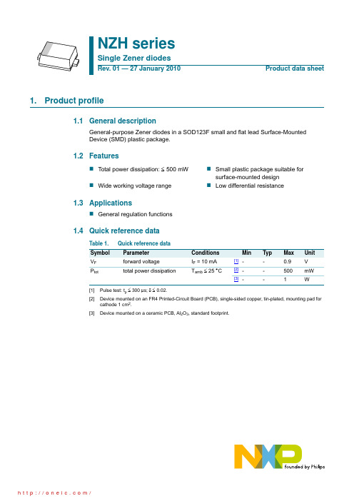
thermal resistance from junction to solder point
Min Typ Max Unit
[1] -
-
250 K/W
[2] -
-
125 K/W
[3] -
-
70 K/W
[1] Device mounted on an FR4 PCB, single-sided copper, tin-plated, mounting pad for cathode 1 cm2. [2] Device mounted on a ceramic PCB, Al2O3, standard footprint. [3] Soldering point of cathode tab.
Version SOD123F
Table 4. Marking codes
Type number
Marking code
NZH3V0B
CH
NZH3V3A
CJ
NZH3V6B
CK
NZH3V9B
CL
NZH4V3B
CM
NZH4V7B
CN
NZH5V1B
CP
NZH5V6B
CQ
NZH6V2B
CR
NZH6V8B
CS
5. Limiting values
Table 5. Limiting values In accordance with the Absolute Maximum Rating System (IEC 60134).
Symbol Parameter
Conditions
Min
Max Unit
IF Ptot
NZHxxx
山特士汽车连接器说明书

Samtec delivers Sudden Service® solutions for standard and customer-specific automotive designs by providing an array of options to meet the robust quality, production and compliance requirements of our customers. Our automotive interconnect systems are ideal for applications requiring high-performance, high-density, high-reliability / high mating cycles, optics and microelectronics solutions, with varying degrees of PPAP options.STANDARD CATALOG PRODUCT A-SERIES FOR AUTOMOTIVECATALOGACD-SERIESFORCUSTOMIZATIONCertified ISO-9001Built to Samtec’s drawing Sudden Samples for prototyping Short lead timesfor volumeCertified to IATF 16949to support Level 3PPAP requirements– Controlled IATF facility– Registered InternationalMaterial Data System (IMDS)Built to Samtec’sdrawings & standardsShort lead timesfor volumeCertified to IATF 16949to support all agreedupon customer specificrequirements– Controlled IATF facility– Registered InternationalMaterial Data System (IMDS)Vendor Managed Inventoryoptions for volume2From the technology systems inside the cabin, to sensor and lighting systems outside the cabin, designers can create, build and manufacture with the confidence of Samtec quality and support.DRIVER INFORMATIONSYSTEMS (DIS) / AUDIONavigation & TrackingRadar Controlled Cruise ControlGPSSatellite RadioEntertainment SystemsHeads-up Display SystemINTERIORPower Windows & SeatsSunroof, Moonroof ControlsDay / Night MirrorsInterior LightingNight Vision SystemClimate ControlCONTROLInstrument Panel & CockpitSteering ModulesBrake ModulesEngine Control SystemsPower Door LocksAutomatic Transmission (Tiptronic)SAFETYWarning SensorsAnti-theft SystemsSafety Trunk ReleaseHands Free SystemAirbag Release SystemEmergency CommunicationLidar & ADASIR Sensor & Camera Systems35G SOLUTIONS Connectors meet PPAP Level 3 process; cable assemblies are in process.Connectors meet PPAP Level 3 process.SEARAY ™ Open-Pin-Field Arrays EDGE RATE ® Rugged High-Speed Connector Strips SEARAY ™ High-Density Array Cable Assembly 50 Ω High-Frequency RF Flexible Cable Assembly AcceleRate ® Rugged Slim Body Cable Assembly Connected vehicles are the future of mobility. Leveraging next gen 5G networks and cloud services, V2X technologies enable vehicle intelligence, improve traffic flow and increase safety. Samtec’s expanding automotive interconnect portfolio helps route data from 5G radios to sensors throughout the vehicle. Combined with its IATF 16949 certification, Samtec offers technical expertise to support the unique challenges of automotive and transportation applications.CONNECTED VEHICLES V2H V2G V2I V2D V2V V2P E-Mobility is moving automotive technology forward, especially the need for power. Electric cars require DC-DC/AC-DC power conversion, and thermal management for durability and long-life, as well as energy storage and efficient ways to heat or cool the cabin. From charging stations and remote or mobile (vehicle-to-vehicle) charging to a full battery swap, users require options to quickly power their vehicles at home and on the road. Whether inside or outside of the vehicle, Samtec offers a wide variety of interconnects and high-power solutions to meet these needs.E-MOBILITY POWER SOLUTIONS mPOWER ™ Ultra Micro Power Connectors Mini Mate ® Rugged System with Individually Shrouded Contacts PowerStrip ™/30 Amp Signal/Power Combo System One–Piece 2.54 mm Pitch Rugged Interconnect 4FUTURE MOBILITYAutonomous vehicles are a rapidly advancing technology. To meet the industry needs, Samtec offers a broad line of interconnect solutions for all five levels of autonomy, from our Core Products to Silicon-to-Silicon Solutions for full channel signal integrity optimization.LEVEL 0 No Automation Full-time human driver for all aspects of driving.LEVEL 1 Driver Assistance Assistance of either steering or acceleration/deceleration with human driver for all other aspects of driving.LEVEL 2 Partial Assistance Assistance of both steering and acceleration/deceleration with human driver for all other aspects of driving.LEVEL 3 Conditional Automated Driving of all dynamic driving tasks with human driver responding to a prompt to intervene or take control.LEVEL 4 High Automation Automated Driving of all driving tasks under select conditions, without human driver input or oversight.LEVEL 5 Full Automation Full-time Automated Drivingunder all roadway andenvironmental conditions.CORE PRODUCTSOLUTIONSLEVELS 0-5 (PG 8-9)Rugged Tiger Eye™Contact SystemsFlexible Stacking SystemsOne-Piece SystemsMicro Pitch SystemsDiscrete Wire ComponentsSealed I/O SystemsSILICON-TO-SILICONSOLUTIONSLEVELS 3-5 (PG 6-7)High-Density ArraysRugged SI Edge Rate®Contact SystemsEdge Card SystemsGround Plane ConnectorsUltra Micro InterconnectsUltra Micro, High PowerInterconnectsHigh-Speed CableAssembliesRF Cables andComponentsHUMAN MONITORINGMACHINE MONITORING5 LEVELS OF AUTONOMY5HIGH-DENSITY ARRAYSSEARAY™ open-pin-field arrays for maximum grounding and routing flexibilitySEARAY™ 0.80 mm pitch arrays provide2x the density of 1.27 mm pitch arraysUp to 720 Edge Rate® contacts for 56 GbpsPAM4 performanceLP Array™ low profile arrays down to 4 mm Compatible with mPOWER™ for signal/power flexibilityEDGE RATE® SYSTEMSRugged Edge Rate® contacts are optimized for signal integrity performance and less prone to damage when “zippered” to unmate56 Gbps PAM4 rugged connectors with1.50 mm contact wipe on 0.80 mm pitchStack heights from 7 mm to 18 mmCompatible with mPOWER™ for signal/power flexibilityHIGH-SPEED EDGE CARD SYSTEMS 0.80 mm and 1.00 mm pitch with up to 200 total pins Vertical, right-angle and edge mountRugged edge card/power combinationLatches and weld tabs available GROUND PLANE CONNECTOR STRIPSSurface mount ground plane between signal rowsfor improved electrical performanceIntegral metal plane for power to 25 Amps Increased 1.20 mm contact wipe for a reliable connection in rugged applicationsCompatible with mPOWER™ for signal/power flexibility 6ULTRA-MICRO INTERCONNECTSRazor Beam ™ LP connectors on 0.40 mm and 0.50 mm pitchUltra low stack heights down to 2 mmRazor Beam ™ hermaphroditic connectors4-6x greater mating/unmating forces vs. typical micro pitch connectorsmPOWER ™ ULTRA MICRO POWER INTERCONNECTSMicro 2.00 mm pitch with up to 21 Amps per bladeDesign flexibility for power-only or power/signal applicationsSmall form factor allows space for other components on the boardSelectively loaded contacts for creepage and clearance requirements30 A solution in developmentHIGH-SPEED CABLE ASSEMBLIES0.80 mm pitch Edge Rate ® coax and twinax assembliesHermaphroditic Razor Beam ™ coax assemblies with rugged shielding0.50 mm and 0.80 mm pitch integral ground plane assembliesEye Speed ® cable for excellent signal integrity, small bend radii and dynamic high flexing cyclesACCELERATE ® SLIM BODY CABLE ASSEMBLIESSlimmest cable assembly in the industry at 7.6 mm body widthEye Speed ® ultra low skew twinax cableRugged metal latching system and shielded board level mateSupports 56 Gbps PAM4 applicationsRF CABLE AND COMPONENTSSMP and SMPM miniature push-on connectors to 65 GHzMicro-miniature interconnects with snap on-coupling; high vibration availableShielded twisted pair system with high-reliability contactsHigh frequency cable to 10 GHz with U.FL/W.FL compatible plugsSamtec’s Silicon-to-Silicon Solutions are available as standard catalog products and automotive A-Series, or customer-specific automotive ACD-Series. For more information or to discuss your specific automotive application, please contact *************************. 7FLEXIBLE STACKING SYSTEMS0.80 mm to 2.54 mm pitch systemsPass-through contacts to connect multiple boardsUp to six rows and 300 total pinsLow profile and skyscraper solutionsContact flexibilityONE-PIECE SYSTEMSRobust design and mechanical hold-downs for high shock and vibration applications1.00 mm and .100" (2.54 mm) pitchProfiles up to 10 mmVertical and right-angle applicationsTIGER EYE ™ CONTACT SYSTEMSHigh-reliability multi-finger, BeCu contact system for rugged environments and high cycle applications0.80 mm, 1.27 mm and 2.00 mm pitch systemsOptional ruggedizing features, including alignment pins, weld tabs and screw downsVertical and right-angle for parallel, perpendicularor coplanar applicationsCONTACT FLEXIBILITYTIGER CLAW ™Pass-ThroughTIGER EYE ™High-Reliability TIGER BUY ™High-Retention POWER EYEHigh-CurrentRUGGED FEATURES Friction LocksGuide Posts Screw Downs Alignment Pins 8MICRO PITCH SYSTEM0.50 mm pitch with up to 60 contacts Mitigates misalignment in X and Y directions Choice of body heightIdeal for multiple connectors on a board DISCRETE WIRE COMPONENTS 1.00 mm to 2.54 mm pitchdiscrete wire componentsHigh-reliability Tiger Eye™multi-finger BeCu contact systemMini Mate® rugged shroudeddiscrete wire componentsSingle and double rowRugged latching and polarizationACCLIMATE™ IP68 SEALED CIRCULAR SYSTEMS Kitted components (Field Termination Kits) for efficient field assemblyChoice of 12 mm (up to 5 A) or 16 mm (up to 11.6 A) metal or plastic shellsTerminals and sockets with 0.50 mm,1.00 mm or 1.50 mm diameter pinsInsertion tools and dust caps availableCUSTOM SOLUTIONS PinModificationsBodyModificationsCustomConnectorsPrototypingSpecialPlatingsTesting QualificationTestingSamtec’s Core Product Solutions are available as standard catalog products and automotive A-Series,or customer-specific automotive ACD-Series. For more information or to discuss your specific automotive application, please contact *************************.9CERTIFICATIONSSamtec is IATF 16949, ISO 14001 and ISO 9001 certified, and is fully integrated with in-house tooling, plating and automated manufacturing capabilities that provide for advanced development, low-cost, quick turn and high volume production. In addition, Samtec is compliant with International Traffic and Arms Regulations (ITAR) and with EU WEEE and RoHS directives. Please visit /quality for additional certification information.RoHS COMPLIANT LEAD FREE CERTIFIED COMPLIANT REACH COMPLIANT IMDS CERTIFIED ISO 14001CERTIFIED ISO 90011. INDEX PAGE2. SERIES DESIGN RECORD — SAMTEC RELEASED PRINT3. CHANGE HISTORY4. SERIES DESIGN FMEA5. PROCESS FLOW DIAGRAM6. PROCESS FMEA7. CONTROL PLAN — PRE-LAUNCH8. CONTROL PLAN — SERIAL PRODUCTION9. MEASUREMENT SYSTEM STUDIES (GAGE R&R) a. Total Gage R&R < 10% is acceptable b. Total Gage R&R >10% , <30% is acceptable for non-critical characteristics 10. ASSEMBLY DIMENSIONAL RESULTS (100% FAI & BALLOONED PRINT) a. Tabular Summary Format (according to AIAG manual) 100% layout for 5 parts for each cavity (1 cavity) 100% layout for 3 parts for each cavity (2 cavities) 100% layout for 2 parts for each cavity (3 or 4 cavities) 100% layout for 1 part for each cavity (6 or more cavities)b. Drawing numbered to correlate with submitted dimensional results and drawing notes PRODUCTION PART APPROVAL PROCESSSamtec uses proven processes that meet our IATF 16949 certification. Samtec designates these products with an A-Series part number. For each A-Series product, a customer will receive a Level 3 Product Part Approval Process (PPAP) package. Contents shown below are the supporting documents required to meet Level 3 PPAP .11. INITIAL PROCESS STUDY (SPC) Cpk > 1.67 or 100% in process inspection 12. COMPONENT PPAP 13. MATERIAL CERTIFICATION 14. QUALIFIED LABORATORY DOCUMENTATION 15. CAPACITY & RUN AT RATE DATA FORM — DATA FROM PRODUCTION TRIAL RUN Data must come from a minimum run of 300 parts 16. RUN @ RATE CHECKLIST17. EVIDENCE OF IMDS SUBMISSIONProof of submission into the International Material Data System 18. PART SUBMISSION WARRANT (PSW)19. FACILITY IATF CERTIFICATION GREEN: SUBMITTED, WHITE: RETAINED 10TESTINGSamtec automotive products are subject to a wide variety of test procedures, from standard testing to those that push the industry limits ensuring quality and durability in any application. Design Qualification Testing includes: Gas Tight, Normal Force, Thermal Aging, mating/unmating/durability, IR/DWV and Current Carrying Capacity (CCC).EXTENDED LIFE PRODUCT™E.L.P.™ products are tested to rigorous standards,which evaluate contact resistance in simulatedstorage and field conditions.• 10 year Mixed Flowing Gas (MFG)• High Mating Cycles (250 to 2,500)• Certain plating and/or contact options will apply• For complete details on Samtec's E.L.P.™program, a list of qualifying products andtest results, visit /ELP or emailthe Customer Engineering Support Groupat **************SEVERE ENVIRONMENT TESTINGSevere Environment Testing (SET) is a new Samtecinitiative to test our products beyond typical industrystandards and specifications, many set forth bycommon requirements for rugged industries. Severalof our products undergo additional testing to ensurethey are more than suitable for industrial, military,automotive and other extreme applications.Contact ************** for more information andtest results as available.TESTING INCLUDES:• Higher Mating Cycles with 100% Humidity• Intense Shock and Vibration: LLCR & Event Detection • Temperature Cycling• Non-Operating Class Temperature• DWV at High Altitude• Electrostatic Discharge (ESD)All Samtec products undergo Design Qualification Testing.SET and E.L.P.™ are complimentary tests in addition to DesignQualification Testing; visit for more information.Customer specific testing is also available; please contact************** for testing capabilities.PITCH TYPE CONTACT SERIES*0.50 mm Q Series® Strip Blade & Beam QSH/QTHBasic Strip Blade & Beam BSH/BTH0.635 mm Q Series® Strip Blade & Beam QSS/QTSBasic Strip Blade & Beam BSS/BTS 0.80 mmEdge Rate® Strip Edge Rate®ERF8/ERM8Edge Card Edge Rate®HSEC8Q Rate® Strip Edge Rate®QRM8/QRF8Q Series® Strip Blade & Beam QSE/QTEBasic Strip Blade & Beam BSE/BTEStrip Tiger Eye™SEM/TEM 1.00 mm Strip Tiger Claw™CLM/FTMH1.27 mmSEARAY™ Array Edge Rate®SEAF/SEAMStrip Tiger Eye™SFM/TFMStrip Tiger Claw™CLP/FTSHStrip Tiger Beam™FLE/FTSH2.00 mm Strip Tiger Eye™SMM/TMMStrip Tiger Claw™CLT/TMMH2.54 mm Strip Tiger Claw™SSM/TSMStrip Tiger Claw™BCS/TSW * Tested socket/terminal combination shown. Other mating headers also available. Contact Samtec if header design you need is not shown.DESIGN QUALIFICATION TESTING10 YEAR MFGEXTENDED LIFEPRODUCTHIGH MATINGCYCLES11© AUGUST 2019, SAMTEC INC.SU D D ENSA M P LEFREE SAMPLES IN 24 HOURSWORLD DIRECT2-DAY SHIPPING TO ALL MAJOR MARKETS3-DAY SHIPPING OF MOST PRODUCTS#1 CONNECTOR MANUFACTURER BISHOP & ASSOCIATESSUPPORT CENTERS MANUFACTURING SALESSAMTEC CABLENEW ALBANY, INDONGGUANCOSTA RICAPENANG JOHORSINGAPOREVIETNAMSAMTEC TOOLSIGNAL INTEGRITY GROUPTUCSON DESIGN CENTERCOLUMBIA DESIGN CENTER SAMTEC OPTICAL GROUPSAMTEC MICROELECTRONICSSCOTTSBURG, INHUIZHOUTAIWANBELGIUMJAPAN。
VITSON产品说明书中文英文

深圳市慧拓鑫科技有限公司Shenzhen Hui Tuo Xin Technology Co., Ltd.产品资料Product information1、TOP电源防雷箱系列(TOP Power lightning protection box series) (1)2、TP 限压型电源防雷模块系列(TP Voltage limiting type power supply lightning protection module series) (8)3、TP直流电源防雷模块系列(TP DC power supply lightning protection module series) (14)4、TCP电源未端精细防护防雷器系列(TCP Power supply terminal fine protective lightning arrester series) (20)5、TDC 电源插座(TDC Power supply lightning protection socket series) (25)6、TV 视频防雷器系列(TV Video arrester series) (30)7、T 视频/射频防雷器系列(T Video / RF lightning arrester series) (36)8、TC控制线路防雷器系列( TC Control circuit lightning arrester series) (40)9、10/100M网络线路防雷器(10/100M Network circuit lightning arrester) (44)10、通讯专线防雷器(Communication line lightning arrester) (49)11、TT天馈线路防雷器系列(TT Antenna line arrester series) (53)1、TOP电源防雷箱系列(TOP Power lightning protection box series)产品介绍Product introductionTOP电源防雷箱系列依据IEC标准设计,8/20波形最大通流容量20KA-100KA,能对电源系统的浪涌电压进行有效的钳制,电源B、C、D级产品均具备。
UL1310 讲义

功率和电流
Not inherently limited 在任何负载下不超过
此类电源具有可以自动切断输出电路的措施。 动作的时间也有要求,除非使用的是经认证符合动作时间要求的且额定 值不大于上表的保险丝。
功率和电流
Not inherently limited 动作时间
ห้องสมุดไป่ตู้
距离
•不同极性带电体间 •带电和不带电金属件间 •带电体和金属外壳间 应满足表24.1和24.2的距离要求 表24.1 – 外壳有开孔 表24.2 – 外壳无开孔
户外产品的额外测试
Rain Test 1小时后, 进行耐压和绝缘电阻测试. Rainproof: 允许进水, 但能高过带电体, 且带电体上不能有水附着. Raintight: 不允许进水.
紫外线测试 & 材料浸水测试 (UL746C) 非金属外壳材料
垫圈材料测试 对用于防水的垫圈材料的弹性和韧性的要求
39.8.3/39.8.4(backfeed)的测试。
非正常测试
Backfeed Protection相关测试 39.8.1/.2: 在充电器输出端接: 1. 指定类型的最大容量和电压的充满的电池,或 2. 空载电压等于充电器额定输出直流源,短路电流不小于200A。 然后在尽可能靠近输出端的地方接能引起最大倒灌电流的阻性负载, 或短路。5秒后读倒灌电流值,不应超过8A。
0.56Nm not for traveler •W 794g •测量时, 输出线不计入其中.
直插式产品
•插头位置 A 5.1mm A 7.9mm (for toy) 直插式产品插入复式插座中的一个时, 不应影响插头完全插 入旁边的其它插座, 除非根本插不进去.
电源线
可接受的电源线
稳压管大全)
3.3V简易开关电源稳压器(1A)
LM1575T-5.0
5V简易开关电源稳压器(1A)
LM1575T-12
12V简易开关电源稳压器(1A)
LM1575T-15
15V简易开关电源稳压器(1A)
LM1575T-ADJ
简易开关电源稳压器(1A可调1.23 to 37)
LM1575HVT-3.3
LM2575HVT-ADJ
简易开关电源稳压器(1A可调1.23 to 37)
LM2576T-3.3
3.3V简易开关电源稳压器(3A)
LM2576T-5.0
5.0V简易开关电源稳压器(3A)
LM2576T-12
12V简易开关电源稳压器(3A)
LM2576T-15
15V简易开关电源稳压器(3A)
LM2576T-ADJ
79L08
-8V稳压器(100ma)
KA1L0380RB
Power Switch
KA5L0380R
Power Switch
KA78R05
Low Dropout Voltage Regulator(1A)
PQ05RD11
ASO保护功能低功耗稳压器(1A)[四端稳压]
PQ05RD21
ASO保护功能低功耗稳压器(2A)[四端稳压]
型号(规格)
功能简介
兼容型号
CA3130
高输入阻抗运算放大器
Intersil[DATA]
CA3140
高输入阻抗运算放大器
CD4573
四可编程运算放大器
MC14573
ICL7650
斩波稳零放大器
LF347(NS[DATA])
带宽四运算放大器
三汇示波器说明书(Ver1.0)
DST4000 和 DST1000 系列数字存储示波器用户手册
i
目录
5.1 显示区 ........................................................................................ 20 5.2 信息区域..................................................................................... 23 5.3 波形显示..................................................................................... 23
三汇系列产品
DST4000 和 DST1000 系列 数字存储示波器
Version 1.0
杭州三汇科技有限公司 www.
目录
目录
目 录 ...........................................................................................................i 版权申明 .......................................................................................................................................................................v 第 1 章 安全事项......................................................................................... 1
tennant v3 操作与零部件手册 - cn - 说明书 用户手册 使用指南

ENCanister Dry Vacuum Cleaner圆桶形干式真空吸尘器/manualsV3Model Part No.:型号部件编号:1070776 -V3 220-240V CN9009724Rev.00 (09-2012)Operator and Parts Manual 操作与零部件手册CNENGLISH 2Tennant V3 (09-2012)EN IntroductionThis manual is furnished with each new model. It provides necessary operation and maintenance instructions and replacement parts information.Read all instructions before using machine.Intended UseThis canister dry vacuum cleaner is suitable for picking up dray, non-flammable dust and debris in an indoorenvironment. It is not suitable for picking up liquids or hazardous materials.General InformationThis machine will provide excellent service. However, the best results will be obtained at minimum costs if: • The machine is operated with reasonable care.• The machine is maintained regularly - per the machine maintenance instructions provided.• The machine is maintained with manufacturer-supplied or equivalent parts.Protect the EnvironmentPlease dispose of packaging materials and used machine components in an environmentally safe way according to local waste disposal regulations. Always remember to recycle.Machine DataPlease fill out at time of installation for future reference. Model No. - Serial No. - Installation Date -Technical Specifications Model V3 Voltage 220-240V Frequency 50-60Hz Rated Power 1200W Airflow Rate 33 l/s Bag capacity 11 L Power Cord Length 12 m Weight 5.75 kg Size (Height x Width) 43cm x 37cm Sound Pressure Level************Construction Class II Vibrations at Controls <2.5 m/s2 Protection Grade IP20Tennant CompanyPO Box 1452, Minneapolis, MN 55440 USA Phone: (800) 553-8033 or (753) 513-2850 Tennant Cleaning Systems & Equipment Co., Ltd Building 1, No. 3777 Caoying Road Qingpu Shanghai, China 201712 phone: (86-21) 6922-53333 fax: (86-21) 6922-5151 Original Instructions. Copyright ©2012 Tennant Company. All rights reserved. Printed in China.Specifications and parts are subject to change without notice.IMPORTANT SAFETY INSTRUCTIONSThis symbol warns the operator of hazards and unsafe practices which could result in severe personal injury or death.WARNING - To reduce the risk of fire, electric shock, or injury:1. Do not leave appliance when plugged in.2. Unplug cord from outlet when not in use and beforeservicing.3. Do not use outdoors or on wet surfaces. This machine isfor indoor and dry use only.4. Do not allow to be used as a toy. Close attention isnecessary when used by or near children.5. Use only as described in this manual. Use onlymanufacturer's recommended attachments.6. Operators shall be adequately instructed on the use ofthis machine.7. This machine is not intended for use by persons(including children) with reduced physical, sensory or mental capabilities, or lack of experience and knowledge, unless they have been given supervision or instruction concerning use of the appliance by a person responsible for their safety.8. Do not use with damaged cord or plug. Regularly inspectcord and plug for damage. If the cord is damaged, it must be replaced by the manufacturer, its service agent or a similarly qualified person in order to avoid a hazard. 9. Do not pull or carry by cord, use cord as handle, close adoor on cord, or pull cord around sharp edges or corners. Do not run appliance over cord. Keep cord away from heated surfaces.10. Do not unplug by pulling on cord. To unplug, grasp theplug, not the cord.11. Do not handle plug or appliance with wet hands. 12. Connect to a properly grounded outlet only.13. Make sure the power voltage corresponds with thevoltage shown on the machine's rating plate.14. Do not put any object into openings. Do not use with anyopening blocked; keep free of dust, lint, hair, and anything that may reduce air flow.15. Keep hair, loose clothing, fingers, and all parts of bodyaway from openings and moving parts. 16. Turn off all controls before unplugging.17. Do not use to pick up flammable or combustible liquids,such as gasoline, or use in areas where they may be present.18. Do not pick up any type of fluid, hazardous dust or toxicmaterials.19. Do not pick up anything that is burning or smoking, suchas cigarettes, matches, or hot ashes. 20. Use extra care when cleaning on stairs.21. Do not use without dust bag and/or filters in place. 22. If using an extension cord make sure the cord rating issuitable for this machine.23. Do not modify machine from its original design.24. Keep children and unauthorized persons away from themachine when in use.25. All repairs must be performed by a qualified serviceperson. Use only manufacturer-supplied or equivalent replacement parts.26. Do not expose to rain or moisture. Store indoors only.SAVE THESE INSTRUCTIONSStorage and TransportingCarefully wrap power cord around machine's cord hooks and store machine in a dry indoor environment. Do not expose machine to rain or moisture. Lift machine by the carrying handle to transport.操作坦能V3 (09-2012)3CN介绍本手册提供各款最新型号的说明。
ADG731中文资料
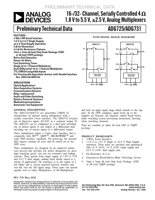
ADG725/ADG731 =REV. PrD May 2002Information furnished by Analog Devices is believed to be accurate andreliable. However, no responsibility is assumed by Analog Devices for its use, nor for any infringements of patents or other rights of third parties which may result from its use. No license is granted by implication or otherwise under any patent or patent rights of Analog Devices.One T echnology Way, P.O. Box 9106, Norwood, MA 02062-9106, U.S.A. T el: 781/ Fax: 781/326-8703Analog Devices, Inc., 200216-/32- Channel, Serially Controlled 4 Ω1.8 V to 5.5 V, ±2.5 V, Analog Multiplexers Preliminary Technical DataPRELIMINARY TECHNICAL DATAFEATURES3-Wire SPI Serial Interface1.8 V to 5.5 V Single Supply±2.5 V Dual Supply Operation4 Ω On Resistance0.5 Ω On Resistance Flatness7mm x 7mm 48 lead Chip Scale Package (CSP)or 48 lead TQFP package.Rail to Rail OperationPower On ResetFast Switching TimesSingle 32 to 1 Channel MultiplexerDual/Differential 16 to 1 Channel MultiplexerTTL/CMOS Compatible InputsFor Functionally Equivalent devices with Parallel InterfaceSee ADG726/ADG732APPLICATIONSOptical ApplicationsData Acquisition SystemsCommunication SystemsRelay replacementAudio and Video SwitchingBattery Powered SystemsMedical InstrumentationAutomatic Test EquipmentGENERAL DESCRIPTIONThe ADG725/ADG731 are monolithic CMOS 32channel/dual 16 channel analog multiplexers with aserially controlled 3-wire interface. The ADG732 switchesone of thirty-two inputs (S1-S32) to a common output, D.The ADG725 can be configured as a dual mux switchingone of sixteen inputs to one output or a differential muxswitching one of sixteen inputs to a differential output.These mulitplexers utilize a 3-wire serial interface that iscompatible with SPI TM, QSPI TM, MICROWIRE TM and some DSP interface standards. On power-up, the internal shift register contains all zeros and all switch are in the OFF state.These multiplexers are designed on an enhanced submi-cron process that provides low power dissipation yet gives high switching speed, very low on resistance and leakage currents. They operate from single supply of 1.8V to 5.5V and ±2.5 V dual supply, making them ideally suited to a variety of applications. On resistance is in the region of a few Ohms and is closely matched between switches and very flat over the full signal range. These parts can operate equally well as either Multiplexers or De-Multiplexers PRODUCT HIGHLIGHTS1.3-Wire Serial Interface.2.+1.8 V to +5.5 V Single or ±2.5 V Dual Supplyoperation. These parts are specified and guaranteedwith +5 V ±10%, +3 V ±10% single supply and±2.5 V ±10% dual supply rails.3.On Resistance of 4 Ω.4.Guaranteed Break-Before-Make Switching Action.5.7mm x 7mm 48 lead Chip Scale Package (CSP)or 48 lead TQFP package.FUNCTIONAL BLOCK DIAGRAMSS1S32SCLK DIN SYNCDS1ADAS16AS1BS16BDBSCLK DIN SYNCand have an input signal range which extends to the sup-plies. In the OFF condition, signal levels up to the supplies are blocked. All channels exhibit break before make switching action preventing momentary shorting when switching channels.They are available in either 48 lead CSP or TQFP package.元器件交易网–2–REV. PrDADG725/ADG731–SPECIFICATIONS 1PRELIMINARY TECHNICAL DATAB Version–40°CParameter+25o C to +85°C Units Test Conditions/Comments ANALOG SWITCH Analog Signal Range 0 V to V DD V On-Resistance (R ON )4Ω typ V S = 0 V to V DD , I DS = 10 mA;5.56Ω max Test Circuit 1On-Resistance Match Between 0.3Ω typ V S = 0 V to V DD , I DS = 10 mA Channels (∆R ON )0.8Ω max On-Resistance Flatness (R FLAT(ON))0.5Ω typ V S = 0 V to V DD , I DS = 10 mA 1Ω max LEAKAGE CURRENTSV DD = 5.5 VSource OFF Leakage I S (OFF)±0.01nA typ V D = 4.5 V/1 V, V S = 1 V/4.5 V;±0.25±0.5nA max Test Circuit 2Drain OFF Leakage I D (OFF)±0.05nA typ V D = 4.5 V/1 V, V S = 1 V/4.5 V; ADG725±0.5±2.5nA max Test Circuit 3ADG731±1±5nA max Channel ON Leakage I D , I S (ON)±0.05nA typ V D = V S = 1 V, or 4.5V; ADG725±0.5±2.5nA max Test Circuit 4ADG726±1±5nA max DIGITAL INPUTSInput High Voltage, V INH 2.4V min Input Low Voltage, V INL 0.8V max Input Current I INL or I INH 0.005µA typ V IN = V INL or V INH±0.1µA max C IN , Digital Input Capacitance 5pF typ DYNAMIC CHARACTERISTICS 2t TRANSITION 40ns typ R L = 300 Ω, C L = 35 pF,Test Circuit 5;60ns max V S1 = 3 V/0 V, V S32 = 0 V/3V Break-Before-Make Time Delay, t D 30ns typ R L = 300 Ω, C L = 35 pF;1ns min V S = 3 V, Test Circuit 6Charge Injection ±5pC typ V S = 0 V, R S = 0 Ω, C L = 1 nF;Test Circuit 7Off Isolation-60dB typ R L = 50 Ω, C L = 5 pF, f = 100 kHz;Test Circuit 8Channel to Channel Crosstalk -60dB typ R L = 50 Ω, C L = 5 pF, f = 100 kHz;Test Circuit 9-3 dB Bandwidth ADG72534MHz typ R L = 50 Ω, C L = 5 pF, Test Circuit 10 ADG73118MHz typ C S (OFF)13pF typ f = 1 MHz C D (OFF) ADG725180pF typ f = 1 MHz ADG731360pF typ f = 1 MHz C D , C S (ON) ADG725200pF typ f = 1 MHz ADG731400pF typ f = 1 MHzPOWER REQUIREMENTS V DD = +5.5 VI DD10µA typ Digital Inputs = 0 V or +5.5 V20µA maxNOTES 1Temperature range is as follows: B Version: –40°C to +85°C.2Guaranteed by design, not subject to production test.Specifications subject to change without notice.(V DD= 5V ± 10%, V SS= 0V, GND = 0 V, unless otherwise noted)元器件交易网–3–REV. PrD ADG725/ADG731PRELIMINARY TECHNICAL DATAB Version–40°CParameter+25o C to +85°CUnits Test Conditions/Comments ANALOG SWITCH Analog Signal Range 0 V to V DD V On-Resistance (R ON )7Ω typ V S = 0 V to V DD , I DS = 10 mA;1112Ω max Test Circuit 1On-Resistance Match Between 0.4Ω typ V S = 0 V to V DD , I DS = 10 mA Channels (∆R ON )1Ω max On-Resistance Flatness (R FLAT(ON))3Ω max V S = 0 V to V DD , I DS = 10 mA LEAKAGE CURRENTSV DD = 3.3 VSource OFF Leakage I S (OFF)±0.01nA typ V S = 3 V/1 V, V D = 1 V/3 V;±0.25±0.5nA max Test Circuit 2Drain OFF Leakage I D (OFF)±0.05nA typ V S = 1 V/3 V, V D = 3 V/1 V; ADG725±0.5±2.5nA max Test Circuit 3ADG731±1±5nA max Channel ON Leakage I D , I S (ON)±0.05nA typ V S = V D = +1 V or +3 V; ADG725±0.5±2.5nA max Test Circuit 4ADG731±1±5nA max DIGITAL INPUTSInput High Voltage, V INH 2.0V min Input Low Voltage, V INL 0.8V max Input Current I INL or I INH 0.005µA typ V IN = V INL or V INH±0.1µA max C IN , Digital Input Capacitance 5pF typ DYNAMIC CHARACTERISTICS 2t TRANSITION 45ns typ R L = 300 Ω, C L = 35 pF Test Circuit 575ns max V S1 = 2 V/0 V, V S32 = 0 V/2 V Break-Before-Make Time Delay, t D 30ns typ R L = 300 Ω, C L = 35 pF;1ns min V S = 2 V,Test Circuit 6Charge Injection ±5pC typ V S = 0 V, R S = 0 Ω, C L = 1 nF;Test Circuit 7Off Isolation-60dB typ R L = 50 Ω, C L = 5 pF, f = 1 MHz;Test Circuit 8Channel to Channel Crosstalk -60dB typ R L = 50 Ω, C L = 5 pF, f = 1 MHz;Test Circuit 9-3 dB Bandwidth ADG72534MHz typ R L = 50 Ω, C L = 5 pF, Test Circuit 10 ADG73118MHz typ C S (OFF)13pF typ f = 1 MHz C D (OFF) ADG725180pF typ f = 1 MHz ADG731360pF typ f = 1 MHz C D , C S (ON) ADG725200pF typ f = 1 MHz ADG731400pF typ f = 1 MHzPOWER REQUIREMENTS V DD = +3.3 VI DD10µA typ Digital Inputs = 0 V or +3.3 V20µA maxNOTES 1Temperature ranges are as follows: B Version: –40°C to +85°C.2Guaranteed by design, not subject to production test.Specifications subject to change without notice.(V DD = 3V ± 10%, V SS = 0V, GND = 0 V, unless otherwise noted)SPECIFICATIONS1元器件交易网–4–REV. PrDADG725/ADG731–SPECIFICATIONS 1PRELIMINARY TECHNICAL DATAB Version–40°CParameter+25o C to +85°C Units Test Conditions/Comments ANALOG SWITCHAnalog Signal Range V SS to V DD V On-Resistance (R ON )4Ω typ V S = V SS to V DD , I DS = 10 mA;5.56Ω max Test Circuit 1On-Resistance Match Between 0.3Ω typ V S = V SS to V DD , I DS = 10 mA Channels (∆R ON )0.8Ω max On-Resistance Flatness (R FLAT(ON))0.5Ω typ V S = V SS to V DD , I DS = 10 mA1Ω max LEAKAGE CURRENTSV DD = +2.75 V, V SS = -2.75 VSource OFF Leakage I S (OFF)±0.01nA typ V S = +2.25 V/-1.25 V, V D = -1.25 V/+2.25 V;±0.25±0.5nA max Test Circuit 2Drain OFF Leakage I D (OFF)±0.05nA typ V S = +2.25 V/-1.25 V, V D = -1.25 V/+2.25 V;±0.5±2.5nA max Test Circuit 3±1±5nA max Channel ON Leakage I D , I S (ON)±0.01nA typ V S = V D = +2.25 V/-1.25 V, Test Circuit 4±0.5±2.5nA max ±1±5nA max DIGITAL INPUTSInput High Voltage, V INH 1.7V min Input Low Voltage, V INL 0.7V max Input Current I INL or I INH 0.005µA typ V IN = V INL or V INH±0.1µA max C IN , Digital Input Capacitance 5pF typ DYNAMIC CHARACTERISTICS 2t TRANSITION 40ns typ R L = 300 Ω, C L = 35 pF Test Circuit 560ns max V S1 = 1.5 V/0 V,V S32 = 0 V/1.5 V Break-Before-Make Time Delay, t D 15ns typ R L = 300 Ω, C L = 35 pF;1ns min V S = 1.5 V, Test Circuit 6Charge Injection ±8pC typ V S = 0 V, R S = 0 Ω, C L = 1 nF; Test 7Off Isolation-60dB typ R L = 50 Ω, C L = 5 pF, f = 1 MHz;Test Circuit 8Channel to Channel Crosstalk -60dB typ R L = 50 Ω, C L = 5 pF, f = 1 MHz;Test Circuit 9-3 dB Bandwidth ADG72534MHz typ R L = 50 Ω, C L = 5 pF, Test Circuit 10ADG73118MHz typ C S (OFF)13pF typ C D (OFF) ADG725180pF typ f = 1 MHz ADG731360pF typ f = 1 MHz C D , C S (ON) ADG725200pF typ f = 1 MHz ADG731400pF typ f = 1 MHzPOWER REQUIREMENTS V DD = +2.75 VI DD 10µA typ Digital Inputs = 0 V or +2.75 V 20µA max I SS10µA typ V SS = -2.75 V20µA maxDigital Inputs = 0 V or +2.75 VNOTES 1Temperature range is as follows: B Version: –40°C to +85°C.2Guaranteed by design, not subject to production test.Specifications subject to change without notice.(V DD= +2.5 V ±10%, V SS= -2.5 V ±10%, GND = 0 V, unless otherwise noted)Dual Supply 元器件交易网元器件交易网PRELIMINARY TECHNICAL DATAADG725/ADG731 TIMING C HARACTERISTICS1,2Parameter Limit at T MIN, T MAX Units Conditions/Commentst133ns min SCLK Cycle timet213ns min SCLK High Timet313ns min SCLK Low Timet413ns min SYNC to SCLK falling edge setup timet540ns min Minimum SYNC low timet65ns min Data Setup Timet7 4.5ns min Data Hold Timet833ns min Minimum SYNC high timeNOTES1See Figure 1.2All input signals are specified with tr =tf = 5ns (10% to 90% of V) and timed from a voltage level of (V IL + V IH)/2.DDSpecifications subject to change without notice.Figure 1.3-Wire Serial Interface Timing Diagram.REV. PrD–5––6–REV. PrDADG725/ADG731PRELIMINARY TECHNICAL DATAABSOLUTE MAXIMUM RATINGS 1(T A = +25°C unless otherwise noted)V DD to V SS +7 VV DD to GND –0.3 V to +7 V V SS to GND +0.3 V to -7 VAnalog Inputs 2V SS - 0.3 V to V DD +0.3 Vor 30 mA, Whichever Occurs FirstDigital Inputs 2-0.3V to V DD +0.3 V or30 mA, Whichever Occurs FirstPeak Current, S or D 60mA(Pulsed at 1 ms, 10% Duty Cycle max)Continuous Current, S or D 30mA Operating Temperature Range Industrial (B Version)–40°C to +85°CCAUTIONESD (electrostatic discharge) sensitive device. Electrostatic charges as high as 4000 V readily accumulate on the human body and test equipment and can discharge without detection.Although the ADG725/ADG731 features proprietary ESD protection circuitry, permanent damage may occur on devices subjected to high energy electrostatic discharges. Therefore, proper ESD precautions are recommended to avoid performance degradation or loss of functionality.Storage Temperature Range –65°C to +150°C Junction Temperature +150°C48 lead CSP θJA Thermal ImpedanceTBD°C/W 48 lead TQFP θJA Thermal Impedance TBD°C/W Lead Temperature, Soldering (10seconds)300°C IR Reflow, Peak Temperature +220°CNOTES 1Stresses above those listed under “Absolute Maximum Ratings” may cause permanent damage to the device. This is a stress rating only and functional operation of the device at these or any other conditions above those listed in the operational sections of this specification is not implied. Exposure to absolute maximum rating conditions for extended periods may affect device reliability. Only one absolute maximum rating may be applied at any one time.2Overvoltages at SCLK, SYNC , DIN , RS , S or D will be clamped by internal diodes.Current should be limited to the maximum ratings given.ORDERING GUIDEModel Temperature Range Package Description Package Option ADG725BCP -40 o C to +85 o C Chip Scale Package (CSP)CP-48ADG725BSU -40 o C to +85 o C Thin Quad FlatpackSU-48ADG731BCP -40 o C to +85 o C Chip Scale Package (CSP)CP-48ADG731BSU-40 o C to +85 o CThin Quad FlatpackSU-48元器件交易网ADG725/ADG731–7–REV. PrDPRELIMINARY TECHNICAL DATAPIN FUNCTION DESCRIPTIONADG725ADG731Mnemonic Function SCLKSerial Clock Input. Data is clocked into the input shift register on the falling edge of the serial clock input. These devices can accomodate serial input rates of up to 30MHz.R S Active low control input that clears the input register and turns all switches to the OFF condition.DIN Serial Data Input. Data is clocked into the 8-bit input register on the falling edge of the serial clock input.SXX Source. May be an input or output.D X Drain. May be an input or output.V DD Power Supply Input. These parts can be operated from a supply of +1.8V to +5.5V and dual supply of +/-2.5V.G N D Ground reference.SYNCActive Low Control Input. This is the frame synchronization signal for the input data. When SYNC goes low, it powers on the SCLK and DIN buffers and the input shift register is enabled. An 8-bit counter is also enabled. Data is transferred on the falling edges of the following clocks. After 8 falling clock edges, switch conditions are automaticaly updated. SYNC may be used to frame the signal, or just pulled low for a short period of time to enable the counter and input buffers.PIN CONFIGURATIONSCSP & TQFPS28S27S26S25S24S23S22S12S11S10S9S8S7S6S5S4S3S2S21S20S19S18S1S17S 13S 14S 15S 16N CDN CN CS 32S 31S 30S 29V D DV D DN CN CS Y N CD I NS C L KN CN CN CG N DV S SS12B S11B S10B S9B S8B S7B S6B S12A S11AS10A S9A S8A S7A S6A S5A S4AS3A S2A S5B S4B S3B S2B S1A S1BS 13AS 14AS 15AS 16AN CD A N CD BS 16AS 15BS 14BS 13B元器件交易网–8–REV. PrDADG725/ADG731PRELIMINARY TECHNICAL DATATable 2. ADG731 Truth TableA4A3A2A1A0E N C S Switch Condition X X X X X X 1Retains previous switch condition X X X X X 11All Switches OFF 0000000100001002000100030001100400100005001010060011000700111008010000090100100100101000110101100120110000130110100140111000150111100161000000171000100181001000191001100201010000211010100221011000231011100241100000251100100261101000271101100281110000291110100301111000311111132X = Don’t CareTable 1. ADG725 Truth TableA3A2A1A0E N C S A C S B Switch ConditionX X X X X 11Retains previous switch condition X X X X 111All Switches OFF 0000000S1A - DA, S1B - DB 0001000S2A - DA, S2B - DB 0010000S3A - DA, S3B - DB 0011000S4A - DA, S4B - DB 0100000S5A - DA, S5B - DB 0101000S6A - DA, S6B - DB 0110000S7A - DA, S7B - DB 0111000S8A - DA, S8B - DB 1000000S9A - DA, S9B - DB 1001000S10A - DA, S10B - DB 1010000S11A - DA, S11B - DB 1011000S12A - DA, S12B - DB 1100000S13A - DA, S13B - DB 1101000S14A - DA, S14B - DB 1110000S15A - DA, S15B - DB 1111S16A - DA, S16B - DB元器件交易网ADG725/ADG731–9–REV. PrD PRELIMINARY TECHNICAL DATAV DD Most positive power supply potential.V SS Most Negative power supply in a dual supply application. In single supply applications, connect to GND.I DD Positive supply current.I SSNegative supply current.G N D Ground (0 V) reference.S Source terminal. May be an input or output.D Drain terminal. May be an input or output.I N Logic control input.V D (V S )Analog voltage on terminals D, S R ON Ohmic resistance between D and S.∆R ONOn resistance match between any two channels, i.e. R ON max - R ON minR FLAT(ON)Flatness is defined as the difference between the maximum and minimum value of on-resistance as mea sured over the specified analog signal range.I S (OFF)Source leakage current with the switch “OFF.”I D (OFF)Drain leakage current with the switch “OFF.”I D , I S (ON)Channel leakage current with the switch “ON.”V INL Maximum input voltage for logic “0”.V INHMinimum input voltage for logic “1”.I INL (I INH )Input current of the digital input.C S (OFF)“OFF” switch source capacitance. Measured with reference to ground.CD (OFF)“OFF” switch drain capacitance. Measured with reference to ground.C D ,C S (ON)“ON” switch capacitance. Measured with reference to ground.C INDigital input capacitance.t TRANSITION Delay time measured between the 50% and 90% points of the SYNC and the switch “ON” condi tion when switching from one address state to another.t OPEN“OFF” time measured between the 80% points of both switches when switching from one address state to another.Charge A measure of the glitch impulse transferred from the digital input to the analog output during switching.InjectionOff Isolation A measure of unwanted signal coupling through an “OFF” switch.Crosstalk A measure of unwanted signal is coupled through from one channel to another as a result of parasiticcapacitance.On Response The Frequency response of the “ON” switch.Insertion The loss due to the ON resistance of the switch.LossTERMINOLOGY元器件交易网ADG725/ADG731PRELIMINARY TECHNICAL DATA TYPICAL PERFORMANCE CHARACTERISTICSTBDTPC 1. On Resistance vs. V D(V S) for forSingle SupplyTBDTPC 2. On Resistance vs. V D(V S) forDual SupplyTBDTPC 3. On Resistance vs. V D(V S) forDifferent Temperatures, SingleSupplyTBDTPC 4. On Resistance vs. V D(V S) forDifferent Temperatures, SingleSupplyTBDTPC 5. On Resistance vs. V D(V S) forDifferent Temperatures, Dual SupplyTBDTPC 6. Leakage Currents vs. V D(V S)TBDTPC 7. Leakage Currents vs. V D(V S)TBDTPC 8. Leakage Currents vs. V D(V S)TBDTPC 9. Leakage Currents vs.Temperature元器件交易网–10–REV. PrDADG725/ADG731–11–REV. PrD PRELIMINARY TECHNICAL DATATBD TPC 10. Leakage Currents vs.Temperature TBD TPC 11. Supply Currents vs. InputSwitching FrequencyTBD TPC 12. Charge Injection vs. SourceVoltageTBD TPC 13. T ON /T OFF Times vs.TemperatureTBDTPC 14. Off Isolation vs. FrequencyTBDTPC 15. Crosstalk vs. FrequencyTBDTPC 16. On Response vs. Frequency元器件交易网元器件交易网PRELIMINARY TECHNICAL DATAADG725/ADG731GENERAL DESCRIPTIONThe ADG725 and ADG731 are serially controlled, 32channel and dual/differential 16 channel multiplexers re-spectively.POWER ON RESETOn power up of the device, all switches will be in theOFF condition and the internal shift register is filled withzeros and will remain so until a valid write takes place.SERIAL INTERFACEThe ADG725 and ADG731 have a three wire serial inter-face (SYNC, SCLK, and DIN), which is compatible withSPI, QSPI, MICROWIRE interface standards and mostDSP’s. Figure 1 shows the timing diagram of a typicalwrite sequence.Data is written to the 8-bit shift register via DIN underthe control of the SYNC and SCLK signals.When SYNC goes low, the input shift register is enabled.An 8-bit counter is also enabled. Data from DIN isclocked into the shift register on the falling edge ofSCLK. Figures 2 & 3 show the contents of the input shiftregisters for these devices. When the part has receivedeight clock cycles after SYNC has been pulled low, theswitches are automatically updated with the newconfiguration and the input shift register is disabled. WithSYNC held high, any further data or noise on the DINline will have no effect on the shift register.The ADG725 CSA and CSB data bits allow the user theflexibility to change the configuration of either or bothbanks of the multiplexer.–12–REV. PrDADG725/ADG731–13–REV. PrD PRELIMINARY TECHNICAL DATATest Circuit 1.On Resistance.Test Circuit 2.I S (OFF).D Test Circuit 4.I D (ON)Test Circuit 5.Switching Time of Multiplexer, t TRANSITION .Test Circuit 6.Break Before Make Delay, t OPEN .V V DVV DVV OUTTRANSITIONTRANSITIONSYNCV OUT* SIMILAR CONNECTION FOR ADG7250V V V V V V V OUTV 0VV S SYNC*SIMILAR CONNECTION FOR ADG725V 元器件交易网–14–REV. PrDADG725/ADG731PRELIMINARY TECHNICAL DATATest Circuit 7.Charge Injection.Test Circuit 8.OFF IsolationTest Circuit 9.Channel-to-Channel Crosstalk.V *SIMILAR CONNECTION FOR ADG725V*SIMILAR CONNECTION FOR ADG725OFF ISOLATION = 20 LOGOUT V SCHANNEL TO CHANNEL CROSSTALK=20LOG 10(V OUT /V S )*SIMILAR CONNECTION FOR ADG725Test Circuit 10. Bandwidth*SIMILAR CONNECTION FOR ADG725INSERTION LOSS = 20 LOG VOUT WITH SWITCHVOUT WITHOUT SWITCH元器件交易网ADG725/ADG731–15–REV. PrD PRELIMINARY TECHNICAL DATAOUTLINE DIMENSIONSDimensions shown in inches and (mm).48-Lead CSP (CP-48)48-Lead TQFP(SU-48)0.006 (0.17)BSC0.024 (0.60) 0.017 (0.42) 0.012 (0.30) 0.009 (0.23) BSC PIN 1CONTROLLING DIMENSIONS ARE IN MILLIMETERS0.035 (0.90) MAX 0.033 (0.85) NOMREF元器件交易网。
TDA7313中文资料
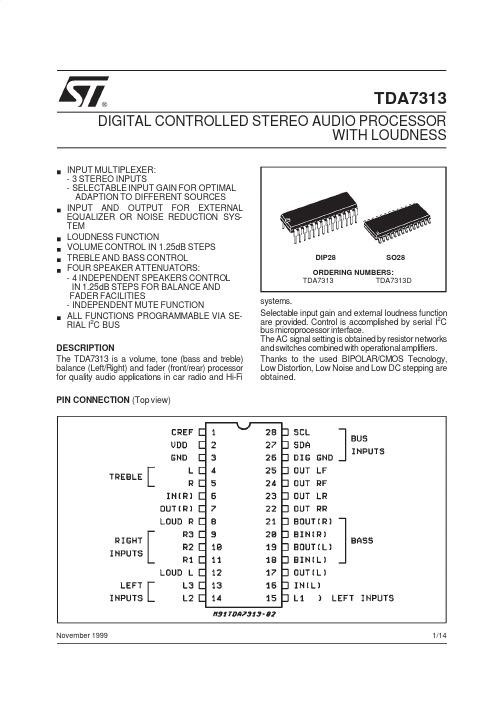
TDA7313
3/14
元器件交易网
TDA7313
ELECTRICAL CHARACTERISTICS (refer to the test circuit Tamb = 25°C, VS = 9V, RL = 10KΩ, RG = 600Ω, all controls flat (G = 0), f = 1KHz unless otherwise specified)
35 37.5 40
0.5 1.25 1.75
1.5
80
100
0
3
1
10
Gb
Control Range
BSTEP
Step Resolution
RBБайду номын сангаас
Internal Feedback Resistance
TREBLE CONTROL (1)
Max. Boost/cut
+12 +14 +16
1
2
3
34
44
Input Resistance Clipping Level Input Separation (2) Output Load resistance Min. Input Gain Max. Input Gain Step Resolution Input Noise DC Steps
VOLUME CONTROL
58
Gt TSTEP
Control Range Step Resolution
Max. Boost/cut
+13 +14 +15
1
2
3
Unit
V mA dB
KΩ Vrms
E3S-CD12中文资料(omron)中文数据手册「EasyDatasheet - 矽搜」
Distance (m)
工作范围 Parallel Operating Range
(典型值)
E3S-CTj6
Y X
Operating Range (Typical) E3S-CDj6 (Left and Right)
E3S-CDj7 and E3S-CDj2 (Left and Right)
Set distance x (c m )
Note.)
Blue
0V
ZD : VZ = 39 V Note: 设置NPN和PNP输出选择器NPN
.
Light indicator
(R e d )
Stability indicator
P hoto(Green) e) lec tric
sensor main c irc uit
PNP output transistor NPN and PNP output selector NPN output transistor
Parallel operating range Y (cm)
Detecting distance X(m)
Operating position Y(mm)
Set distance x (c m ) Sensing object
Y
X
Detecting distance X(cm)
Operating position Y(m)
Brown 10 to 30 VDC
Black Control output
(S ee Note.)
Load
Blue
Load current
0V
ZD : VZ = 39 V Note: 设置NPN和PNP输出选择器PNP
HT7133规格书
4.268 4.400 4.532
V
IOUT
输出电流
6.4V
—
20
30
—
mA
∆ VOUT
负载调整率
6.4V 1mA ≤ IOUT ≤ 30mA
—
15
45
mV
VDIF
压降 ( 注 )
— IOUT=1mA, ∆ VOUT=2%
—
35
55
mV
ISS
D V OUT D V IN ´ V O U T
耗电流 输入电压调节率
Ta=25°C 单位
VOUT
输出电压
5.6V IOUT=10mA
3.492 3.600 3.708
V
IOUT
输出电流
5.6V
—
20
30
—
mA
∆ VOUT
VDIF
ISS
D V OUT D V IN ´ V O U T
VIN
D V OUT D T a´ V O U T
负载调整率 压降 ( 注 ) 耗电流 输入电压调节率 输入电压 温度系数
—
35
100
mV
ISS
D V OUT D V IN ´ V O U T
耗电流 输入电压调节率
4.5V 无负载
—
2.5
4.0
— 3.5V ≤ VIN ≤ 30V, IOUT=1mA
—
0.1
0.2
µA %/V
VIN
输入电压
—
—
—
—
30
V
D V OUT D T a´ V O U T
温度系数
4.5V IOUT=10mA, -40°C<Ta<85°C
常用电源及稳压芯片名称(大部分是TI的)
常用电源及稳压芯片名称(大部分是TI的)估计就知道这些芯片的大概功能。
收藏吧LM2930T-5.0 5.0V低压差稳压器LM2930T-8.0 8.0V低压差稳压器LM2931AZ-5.0 5.0V低压差稳压器(TO-92)LM2931T-5.0 5.0V低压差稳压器LM2931CT 3V to 29V低压差稳压器(TO-220,5PIN)LM2940CT-5.0 5.0V低压差稳压器LM2940CT-8.0 8.0V低压差稳压器LM2940CT-9.0 9.0V低压差稳压器LM2940CT-10 10V低压差稳压器LM2940CT-12 12V低压差稳压器LM2940CT-15 15V低压差稳压器LM123K 5V稳压器(3A)LM323K 5V稳压器(3A)LM117K 1.2V to 37V三端正可调稳压器(1.5A)LM317LZ 1.2V to 37V三端正可调稳压器(0.1A)LM317T 1.2V to 37V三端正可调稳压器(1.5A)LM317K 1.2V to 37V三端正可调稳压器(1.5A)LM133K 三端可调-1.2V to -37V稳压器(3.0A)LM333K 三端可调-1.2V to -37V稳压器(3.0A)LM337K 三端可调-1.2V to -37V稳压器(1.5A)LM337T 三端可调-1.2V to -37V稳压器(1.5A)LM337LZ 三端可调-1.2V to -37V稳压器(0.1A)LM150K 三端可调1.2V to 32V稳压器(3A)LM350K 三端可调1.2V to 32V稳压器(3A)LM350T 三端可调1.2V to 32V稳压器(3A)LM138K 三端正可调1.2V to 32V稳压器(5A)LM338T 三端正可调1.2V to 32V稳压器(5A)LM338K 三端正可调1.2V to 32V稳压器(5A) LM336-2.5 2.5V精密基准电压源LM336-5.0 5.0V精密基准电压源LM385-1.2 1.2V精密基准电压源LM385-2.5 2.5V精密基准电压源LM399H 6.9999V精密基准电压源LM431ACZ 精密可调2.5V to 36V基准稳压源LM723 高精度可调2V to 37V稳压器LM105 高精度可调4.5V to 40V稳压器LM305 高精度可调4.5V to 40V稳压器MC1403 2.5V基准电压源MC34063 充电控制器SG3524 脉宽调制开关电源控制器TL431 精密可调2.5V to 36V基准稳压源TL494 脉宽调制开关电源控制器TL497 频率调制开关电源控制器TL7705 电池供电/欠压控制器7805 正5V稳压器(1A)7806 正6V稳压器(1A)7808 正8V稳压器(1A)7809 正9V稳压议(1A)7812 正12V稳压器(1A)7815 正15V稳压器(1A)7818 正18V稳压器(1A)7824 正24V稳压器(1A)7905 负5V稳压器(1A)7906 负6V稳压器(1A)7908 负8V稳压器(1A)7909 负9V稳压器(1A)7912 负12V稳压器(1A)7915 负15V稳压器(1A)7918 负18V稳压器(1A)7924 负24V稳压器(1A)78L05 正5V稳压器(100ma)78L06 正6V稳压器(100ma)78L08 正8V稳压器(100ma)78L09 正9V稳压器(100ma)78L12 正12V稳压器(100ma)78L15 正15V稳压器(100ma)78L18 正18V稳压器(100ma)78L24 正24V稳压器(100ma)线性稳压器件(输入输出电流相等,压降3V以上)型号稳压(V) 最大输出电流可替代型号79L05 -5V 100mA79L06 -6V 100mA79L08 -8V 100mALM7805 5V 1A L7805,LM340T5LM7806 6V 1A L7806LM7808 8V 1A L7808LM7809 9V 1A L7809LM7812 12V 1A L7812,LM340T12LM7815 15V 1A L7815,LM340T15LM7818 18V 1A L7815LM7824 24V 1A L7824LM7905 -5V 1A L7905LM7906 -6V 1A L7906,KA7906LM7908 -8V 1A L7908LM7909 -9V 1A L7909LM7912 -12V 1A L7912LM7915 -15V 1A L7915LM7918 -18V 1A L7918LM7924 -24V 1A L792478L05 5V 100mA78L06 6V 100mA78L08 8V 100ma78L09 9V 100ma78L12 12V 100ma78L15 15V 100ma78L18 18V 100ma78L24 24V 100ma开关稳压器件(电压转换效率高)型号说明最大输出电流LM1575T-3.3 3.3V简易开关电源稳压器 1ALM1575T-5.0 5V简易开关电源稳压器 1ALM1575T-12 12V简易开关电源稳压器 1ALM1575T-15 15V简易开关电源稳压器 1ALM1575T-ADJ 简易开关电源稳压器(可调1.23V~37V) 1A LM1575HVT-3.3 3.3V简易开关电源稳压器 1ALM1575HVT-5.0 5V简易开关电源稳压器 1ALM1575HVT-12 12V简易开关电源稳压器 1ALM1575HVT-15 15V简易开关电源稳压器 1ALM1575HVT-ADJ 简易开关电源稳压器(可调1.23V~37V) 1A LM2575T-3.3 3.3V简易开关电源稳压器 1ALM2575T-5.0 5V简易开关电源稳压器 1ALM2575T-12 12V简易开关电源稳压器 1ALM2575T-15 15V简易开关电源稳压器 1ALM2575T-ADJ 简易开关电源稳压器(可调1.23V~ 37V) 1A LM2575HVT-3.3 3.3V简易开关电源稳压器 1ALM2575HVT-5.0 5V简易开关电源稳压器 1ALM2575HVT-12 12V简易开关电源稳压器 1ALM2575HVT-15 15V简易开关电源稳压器 1ALM2575HVT-ADJ 简易开关电源稳压器(可调1.23V~37V) 1A LM2576T-3.3 3.3V简易开关电源稳压器 3ALM2576T-5.0 5.0V简易开关电源稳压器 3ALM2576T-12 12V简易开关电源稳压器 3ALM2576T-15 15V简易开关电源稳压器 3ALM2576T-ADJ 简易开关电源稳压器(可调1.23V~37V) 3A LM2576HVT-3.3 3.3V简易开关电源稳压器 3ALM2576HVT-5.0 5.0V简易开关电源稳压器 3ALM2576HVT-12 12V简易开关电源稳压器 3ALM2576HVT-15 15V简易开关电源稳压器 3ALM2576HVT-ADJ 简易开关电源稳压器(可调1.23V~37V) 3A。
NI ELVIS II系列产品规格说明说明书

Arbitrary Waveform Generator/Analog Output
Number of channels.........................2
DAC resolution................................16 bits
DNL.................................................±1 LSB
Maximum working voltage for analog inputs (signal + common mode) ................ ±11 V of AIGND
CMRR (DC to 60 Hz) ..................... 90 dB
Source..............................................AI<0..15>, ScopeCH0, ScopeCH1
Small signal bandwidth (–3 dB)......1.2 MHz
Input FIFO size................................4095 samples
Scanlist memory ..............................4095 entries
Data B signal stream, programmed I/O
希曼顿产品手册

【释义】
在我国工业进入加快发展的新时期、工业发展迎来新的春天的形势下,特别是在市场化、多元 化的竞争发展环境中,我公司将以更加宽阔的视野和长远的眼光谋求新的发展,与社会各界共同促 进我国工业的大繁荣大发展。
开放、包容,就是要通过思想观念的创新和体制机制的创新,按照企业发展的实际需要积极营 造良好的发展环境,努力争取广泛的发展资源。以开放的胸襟增进与各有关方面的沟通与交流,以 包容的心态与同行相互尊重、相互支持。
PAC03I PAC35P XCT1 无纸记录仪 SR150 SR150C 实验室温控单元 DSS
日本岛电 SHIMADEN 中国独家代理 日本 SHIMADEN 岛电仪表 程序控制仪表 FP23 FP93 SRS10 MR13( 三回路 ) 定值控制仪表 SR1/3/4 SR90 SRS10 斜率控制仪表 SR80 SR23 SR253
现主要产品有工业级交流固态继电器、电力调整器(调功 / 调压器)、可控硅模块、可控硅触 发电路板(器)、高校、科研院所用温控实验设备控制电源等。
目前产品已经发展到台湾地区以及国外(印度、巴基斯坦、墨西哥、德国等)。公司自主开发 的现代工厂控制软件平台,使系统更加智能,方便,稳定可靠。
我们公司将不断开发新产品,以满足客户需要; 用杰出的服务与技术,促进海内外市场的发展; 用挡不住的挑战精神,实现希曼顿在温控领域的未来; 从前、现在和将来,无论在那里,希曼顿始终在做温控。 我们真诚欢迎各界朋友来公司参观、考察、洽谈合作,愿与国内外各界朋友进行真诚广泛的技 术交流、贸易和长期的合作。
测量范围代码:
SR1 / SR3 / SR4 系列
4
公司网址: 订购热线:010-62611201/62611202/62611203
74ls373中文资料
型号
tPd
54S373/74S373
7ns
54LS373/74LS373
17ns
PD 525mW 120mW
373 的输出端 O0~O7 可直接与总线相连。
当三态允许控制端 OE 为低电平时,O0~O7 为正常逻辑状态,可用来驱动负载或总
线。当 OE 为高电平时,O0~O7 呈高阻态,即不驱动总线,也不为总线的负载,但
ic中文-17IC中文资料网 - IC中文资料-IC渠道网 IC中文资料 - 电源 - 嵌入式 - 电路图 - 单片机 - 应用方案 - 技术文章
首 页 IC库存 电子资讯 技术资料
IC
非IC
求购信息
PDF 资料
IC库存搜索: 请输入IC型号
搜索
最新搜索: VN2406LZL1 MAX881REUB+T IC42S16400-6TG LTC2230IUP MSR320 HLMP-2700 GS-R405S EPF10K10LI84 …
IC中文资料
型号A开头
型号B 开头
型号C开头
·MCP1316中文资料MCP1317应用MCP1318 MCP1319封装图MC... ·MCP111 中文资料 MCP112 应用 pdf 封装图 管脚说明... ·MCP102中文资料MCP103应用MCP111 MCP121封装图MCP131... ·MCP41010 中文资料 MCP41050 应用 pdf MCP41100 封... ·MCP40D17中文资料 MCP40D18应用 pdf MCP40D19 封装图... ·DS12R885 中文资料 DS12CR887 应用 pdf DS12R887封... ·MAX6972ATJ 中文资料 MAX6973ATJ 应用 pdf 封装图 管脚... ·MCP14E3中文资料MCP14E4 应用 pdf 封装图 MCP14E5管脚说... ·MCP6V06中文资料 MCP6V07应用 pdf 封装图 MCP6V08管脚说... ·MCP6V01中文资料MCP6V02应用 pdf 封装图MCP6V03 管脚说明...
Denison Hydraulics 12V,3000mA IP67插头驱动器说明书
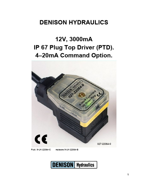
2
12V, 3000mA Plug Top Driver Unit.
Product Advantages:
Important Notes:
EMC compliant product to EN50081-1 and EN50082-2 ( heavy industrial ) 1 x proportional MosFet driver output ( PWM ) at upto 3 amps ( @12VDC ). Field and time tested and proved electronic circuit design. 4-20mA command Input signal capability. No extra DIN housing or ‘Card Holder’ to buy. Comes complete with 3 metres of colour coded wire for fast connection. Product integrity maintained under extreme operational environments. Fully ‘isolated’ design for improved safety and ease of application difficult areas. Self contained driver plug needing only an external 4-20mA command. Unique, Small, light weight unit with ‘Blend-Anywhere’ colour/design. Unit status ‘Diagnostic’ LED visible through opaque plug cover. Low cost compared to other available modules with comparative functions. Easy to use ‘top entry’ adjustments for all major parameters. ‘Encapsulated’ version to suit application environment. Separate Linear Ramp ‘UP’ and Ramp ‘Down’ ( single turn ) adjustments. Multiturn potentiometer ( 20 turns ) ‘I Min’ adjustment for driven solenoid Multiturn potentiometer ( 20 turns ) ‘I Max’ adjustment for driven solenoid. ‘Ruggedised’ design allowing use on ‘Internal’ OR ‘External’ applications. Heavy duty approved cable for all application environments. ‘Dither’ frequency Variable ( single turn ) from 100Hz to 250Hz ( +/-20%). ‘ON-Valve’ mounting using standard DIN connector for space saving. Flame proof resin encapsulation. Protected inputs and user outputs for maximum reliability and product life.
PumLantern SCC3733产品说明书

This page is intentionally left semi-blank.Y eah, it was going to be completely blank, but we needed to put that boring legal-type stuff somewhere. We were going to say “use this marvelous empty page as you blank canvas with which to create such illustrations or notes as to change the very fabric of society.” Instead it’s now a partially text-populated page with a large and awkward empty portion in the middle. Feel free to use it however you want.Boring Legal-Type Stuff:“SOLARBOTICS” is a trademark of Solarbotics Ltd. Reg. CIPO / USPTO.Disclaimer of LiabilitySolarbotics Ltd. is not responsible for any special, incidental, or consequential damages resulting from any breach of warranty, or under any legal theory, including lost profits, downtime, good-will, damage to or replacement of equipment or property, and any costs or recovering of any material or goods associated with the assembly or use of this product. Solarbotics Ltd. reserves the right to make substitutions and changes to this product without prior notice.L a n t e r n S i d e s x 4L a n t e r n T o p x 1CP1000 F x2µ74HCT240 x1SCC3733 x1DC-20 Pin Chip Carrier x1CP0.47 x5µD2 x1SBLED x4SWire x5”R100k x1R1.5M x1R2.2M x1R4.7M x1R6.8M x1BHoldAAA x1Ba ttA AA x2DSST x1Circuit Board V e l l u m x 1Let’s get started. Start by opening your bag of parts, and dumping them into a safe place like an egg-container (remove eggs), pie-plate (eat the pie), or cat-food bowl (give cat away to gypsies). Don’t simply spread them about on a table-surface where they’ll roll away, because then you’ll think we forgot something in the kit and have to call us. Then we’ll tell you to look under your chair, and you’ll find it there and think we have magic powers. In short, keep your parts safe when you dump them out - they’re small, and will try their hardest to hide from you!Bad No flow from leg to pad GoodFlows from leg to padBadSolder “bridge” across pads Bad & Good Solder JointsXXRemember to take your time. Don’t rush.It’s almost impossible to “burn up” these parts!The most important skill needed to successfully construct your device is soldering. Make sure you start by using electronics solder, not plumber’s solder. The main trick to getting a successful solder connection is to heat the junction up before applying the solder to the heated area. Do NOT try to melt some solder onto the tip of the iron and smear it onto the joint - you won’t get a strong joint.If the heat is applied unevenly, you will get solder blobs (see below). T o better apply heat,keep your soldering iron tip clean by wiping it frequently on a damp sponge or cloth. The tip should always be shiny, and not covered in tarnish and burned crud (don’t burn crud - bad!).Y ou’re a roboticist, not a painter!Let’s start with mounting the chipcarrier to the printed circuitboard (PCB).It makes it easier toinstall the actual chip later.Note the notch on the carrier,and make it match the notch onthe PCB.Installation hint: Put the carrierin, then fold over a leg or two tokeep it locked in. It keeps it fromfalling out!Chip Carrier NotchThe way the PumLantern “Pums” is determined by resistors R1 and R2 - the bigger the resistor, the longer the time interval between Pums. Some people like frequent blips; others more sleepy longer intervals. Or mix ’em up for a more random light show.Choose what Pum interval you’d like:0.3 seconds - use 1.5M (Brown, Green, Green)0.6 seconds - use 2.2M (Red, Red, Green)1 seconds - use 4.7M (Yellow, Purple, Green)1.5 seconds - use 6.8M (Blue, Grey, Green)R1 controls the Pum behavior of LED1 & LED2; R2 controls LED3 & LED4. Not that it really matters, but some people like to have fanatical control over how their devices work.May we suggest you start with the 2.2M and 6.8M?Did you pay close attention to those soldering instructions? Well, now it’s time to put your new skill to use...1.5M (Brown, Green, Green)2.2M (Red, Red, Green)4.7M (Y ellow, Purple, Green)6.8M (Blue, Grey, Green)Start by installing your selected R1 and R2 resistors. Put the 100k resistor (Brown / Black / Y ellow) for position R3. R3 sets the dark “turn-on”sensitivity . Lower values make it turn on earlier in the evening. Be careful installing the D1 diode! Note the position of the band, and make it match the position printed on the PCB!Step 3a: R3100k Resistor(Brn/Blk/Yel)Step 3b: R12.2M Resistor (Red/Red/Grn)(or your choice)Step 3d: R24.7M Resistor (Yel/Purp/Grn)(or your choice)Four capacitors work with the R1 and R2 resistors to make the timingcircuit that drives the PumLantern. The fifth capacitor works with the 100k R3 resistor’s “dark turn-on” circuit.These capacitors don’t care which way they are installed. Just snug them down to the PCB, solder them in, and clip off the extra leads.Step 4: Install 0.47µFcapacitors in locationsC3, C4, C5, C6, and C7.(Y es, we know we skippedC1 and C2, but we’ll getback to them - honest)Tip:After you put the part in, bend theleads so it stays in while you solder!Step 3c: D1 Diode Note where the band is!Light Emitting Diodes (”LEDs”) make the light. The ones in your kit are sooper-dooper bright, designed for maximum PUM. Some have a flat top, which makes them spread their light even wider than the regular type. Important things to learn about LEDs: They have a cathode (-) and an anode (+), which means you have to learn which is which. There are 3 easy ways:1) The anode is the longer leg. Remember this by thinking ofthe + sign as two legs ( “|” and a ” –” ). Add these lengths up,and it’s longer than the cathode (just “ –” ).2) If you look carefully at the LED itself, you will see it has aflat shoulder, which marks the cathode ( – ).3) Look carefully into the LED. The cup side is always thecathode ( – ).Method 1: Longer lead = Anode ( + ) Method 2:Flat spot = Cathode ( – )Method 3: LED Cup = Cathode ( – )Y our PumLantern lights the LEDs up in pairs LED1 & LED3, and LED2 & LED4, so if you want to colour-arrange your LEDs, here is an easy way to check them.Step 1: Arrange LED soanode (+) matches solarcell’s oval pad, andcathode (–) matchesrectangular pad Step 2: Pinch downthe leads to the padshard with your thumband finger.Step 3: Hold up to lamp. Look at the pretty colour!With all this knowledge, now you won’t have any problem installing the LEDs so the cathode side matches the flat-spot marked on the PCB in spots LED1-4, right?Install, solder, snip!Step 5: Install the LEDs in locationsLED1 - 4, matching flat spot on the LEDsto flat drawn on PCB.Installation check: ALL the LED cups will look the same. Eitherthey will be all right, or all wrong (we have confidence in you!)The 1000µF capacitors actually store the extra “Pum” power in the circuit. Fold them like this. Just like this. One cap’s leads to the right, the other cap’s leads to the left.See the stripe on the side? That’s the cathode, which should be easy for you to identify because you’re expert at identify-the-cathode-by-the-lead-length now.Step 6: Bend 1000µF capacitor leadsover right next to capacitor body. Oneto the right, the other to the left.Step 7: Install capsso long lead goesthrough “+” padRemember the first step where we put in the chip carrier? Let’s put it to work. We’re almost ready to power-test your Pummer!Find the chip, and put it in the carrier, so the notch matches the notch on the carrier. Y ou might find it easier to put it in the carrier after bending in the legs a bit by laying the legs on a surface and gently bending it over.Step 8: Install 74HCT240 into thecarrier. Note the notch positionon the chip and carrier, andmake them match!We had you fold over the capacitor leads beforesoldering them in so you are sure not to leavethem standing straight up. If you do, they caststrange shadows on the inside of yourPumLantern.Make sure you install thecapacitors correctly . The longerlead (anode +) is marked on theboard with a “+”, and is also theround pad. The cathode (–) is the square pad.Time to see how good your soldering is!Hopefully your batteries will have some charge. If not, charge’em up, or use a pair of AAA cells (borrowed from a remote control), and stick them into the AAA cell holder.Insert the battery holder from the underside (opposite side to where you’ve done all your work so far), and give it a bit of a bend so the leads make a secure contact with the PCB. If all is well, you should see your 4 LEDsjumping to life in a pleasant, pummer-ish manner...Step 9a: Put fresh batteries in the holder,and insert it from the bottom. These holesare labeled “Batt” on the top of the PCB.Step 9b: Tilt the board to the batteryholder pins so that they are for suremaking contact.Step 9c: Inspect your handiwork!Y ou should see 4 blinky lights!If you don’t see blinky lights, check:!Batteries charged?!Chip in right-way around?!LEDs in right-way around?There’s not much else that can gowrong, so if nothing else, re-touch up your soldering!Step 10b: Wire red to oval pad, and black to square padIf you are sure all is well with your pummer, then go ahead and snug the battery pack up to the back of the PCB. Solder it in and snip the leads.Step 10a: Wire red to “Solar +” and black to square padPull the battery pack off, so it’s easier to solder the solar cell wires to the PCB. This is pretty straightforward if you remember to solder red to “+” and black to “–“.Strip off a bit of insulation from the end of the wire by firmly pinching and pulling it off between your thumbnail and index finger. Or use a properwire-stripping tool if you wish (but it’s not as much fun). Solder the red wire to the PCB pad “Solar +”, and the black to the square pad next to it.Do the same on the solar-cell end of the wire, red to the oval pad, and black to the rectangle pad.If all is well, when you hold the solar cell up to the light, the pummer will stop working (and start recharging). Cover it with your hand, and it should kick back to life!Y Red (+)Black (–)Except your liver - you need that part. Our laser-cut art should come out easily, but if not, use a sharp knife to gently pop it out of the frame.We’ve done a lot of work to make assembly nice and tidy . Be gentle (especially with delicate art), and it’ll turn out fine!We’ve placed a little slit into the top of the lantern, so all you have to do is flex the board and slip the wire through the slot into the hole.We’re not going to hold your hand and tell you about “Slot A ”s and “T ab B”s. Y ou’re old enough to figure out what goes where. Just leave one side completely open.Fold in half...then unfold.Fold side 1 to middleFold side 2 to middleUnfold until it holds a sorta box-shapeFold the vellum paper in half, then fold each end in 1/4 again.Not clear? Here’s some pictures:Place the vellum inside the lantern, so thateach side sits flush with the lantern shell.Use some careful tweaking, and you should be able to mount the final side to thePumLantern without problem.See those two notches on thebottom? Y ou need to get the tabs on the end of your completed board in there. Push the PCB into one slot, then flex the other side until you canpop the other tab into place.Before you mount your cell, you might want to think about where your Pumlantern will live. It may be best for the solar cell to be attached to one side instead of the top, so it better catches sunlight from a window.Peel one side of your double-sided sticky tape, and press it onto the solar cell.Then peel the other side and press itonto the top of the lantern. All done!There’s two parts to the PumLantern. The “dark turn-on” circuit, and the actual Pum circuit. Let’s start with the Pum circuit!The Pummer is based around a very simple BEAM circuit called a “Bicore”, which is simply an oscillator that has two outputs that change voltage.When one is “high” (3V), the other is “low” (0V). Every so often, they trade voltages.We’re using this “trade voltage” behavior to create a charge-pump, which is a fancy way of saying we’re building something that makes more voltage than what it normally access to. Here’s how it works (showing only one pair of LEDs in operation):hasWith the bicore output + / -, it charges the capacitor to ~ 1.7V , making LED1The “dark turn-on” circuit is pretty simple. The chip has an “enable-low” line, which means when it sees zero volts, it turns on. We attach this line to the solar cell, and when it stops generating power (sun goes down), the 100kOhm resistor forces the chip on. That simple!Here’s the actual circuit diagram of the PumLantern’s circuit. It’s more useful for those of you who might want to modify your PumLantern, or build a second out of parts.LED3Y ou might have noticed that there are little pads on the tabs that stick out of your PumLantern. Once side has a single square pad, which is the ground pad that connects to common grounds in the circuit.The other tab has two pads: One labeled “S” and one “B”.The “S” pad lets you add an additional solar cell (connected between “S” (+) and the ground pad). This lets you use a large cell and have it power a whole string of lanterns at the same time.The “B” pad lets you directly connect to the battery (with the ground tab) for easy recharging, or measuring voltage.The SolarSpeeder 2 Kit is a very quick Solaroller that can cover 3 meters (10 feet) in under 40seconds in direct sunlight. Simple to construct and a blast to watch, this is a great kit for all beginners!K SS Solarspeeder $27.50 USD/CAD Herbie the Mousebot is a 9-volt battery-powered robot that loves to chase flash light beams. If there are several Herbies in the same area, they can be configured to chase each other! These little robots are so quick, you have to run to keep up to them!K HM Herbie the Mousebot $39.95 USD/CAD201 35th Ave NE N. America T oll Free: 1-866-276-2687Find more neat kits, components, articles, resources and more at our official website:Like the Mousebot, the K PP Photopopper seeks light and avoids obstacles but is solar powered! It’spretty quick, covering a meter per minute (that’s 3.3 feet!). Newly upgraded with better electronics and gold circuit board!K PP Photopopper $45.00USD/CAD。
Sensata 3NT系列定温器规格参数说明书
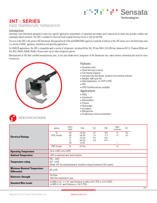
3NT | SERIESFIXED TEMPERATURE THERMOSTATSSPECIFICATIONSAutomatic reset thermostat designed to meet your specific application requirements. Its patented and tamper proof snap action bi-metal disc provides reliable and repeatable switch actuation. The 3NT is suitable for electrical loads ranging from dry circuits to 10A @ 240 VAC.The core of the 3NT is the proven 1NT thermostat. Recognized by UL/CSA and KEMA/ENEC agencies, hundreds of millions of the 1NT device are in the field today used in a variety of HVAC, appliance, automotive and specialty applications.For HVAC/R applications, the 3NT is compatible with a variety of refrigerants, including R410a, R22, R134a, R407c CO2 (R333a), Ammonia (R717), Propane (R290) and A2L (R32, R454A, R454B, R454C). Please reach out for other refrigerant options.Manufactured at ISO 9001 certified manufacturing sites, its dry seal allows direct integration of the thermostat into a wire harness eliminating the need for extra connections.FeaturesApplicationsIntroduction• Automatic reset• Small and easy to mount • Fast thermal response• Innovative dry seal design - protects from moisture and dust • Reliable 100K cycle life• High temperature - to 275ºF (135ºC)• IP67• ATEX-Certified versions available• HVAC• Commercial • Dehumidifiers • Freezers • Heat pumps • Ice makers • Refrigerators• Condensing or moist environmentsElectrical RatingsAgency UL(USA, Canada)ENEC (Europe)STANDARD T EMPERATURES A ND T OLERANCESLOCKING CONNECT ORSHOUSINGO-RINGWIRE LEAD ASSEMB LY1NT T HERMOSTAT3NT CUP3NT DRY SEAL DESIGNImportant Notice:The 3NT is not hermetically sealed, and should not be submerged in liquid. For such applications, please contact Sensata.(1)Minimum bottom temperature of 50ºC (122ºF)TYPICAL PHYSICAL CHARACTERISTICSDimensions in mm (inches)Additional Clips Available for [1/4], [5/16],[1/2], [5/8] t ubesAdditional Clips Available for [1/4], [5/16], [1/2], [5/8] tubesSnap Tube Mount ClipFor 5/8 Inch and 1/2 Inch TubesOpen Tube Mount Clip (3/8 Inch Shown at 90º CCWRotation) 90° and 180° CW Rotations AvailableBasic 3NT DimensionsSurface Mount ClipLocking Tube Mount Clip (3/8 Inch Shown)These devices may not be used as service components, strictly for use by Original Equipment Manufacturer, not repair.USERS ARE SOLELY RESPONSIBLE for design application and function of the end use product. Users must evaluate the suitability of these devices to their application with respect to temperature settings, mechanical cycle life, electrical loading and environmental conditions. This product is not hermetically sealed, it should not be submerged in any liquid. This product is not rated as explosion proof and should not be applied in any application where flammable vapors, gases or dust may be present. End of life failure of this device may result in either open or closed circuit condition. Suitable “End of life” protection should be applied in series with this device per safety agency specifications.IMPORTANT NOTICEORDERING OPTIONS-Temperature Code -Wire Leads -Specifications -Terminals and Mounting ClipPart NumberTemperature CodeDifferentialDifference between Nominal Open and Nominal Close Te mperatureAGENCY A PPROVALS &C ERTIFICATIONSAmericas+1 (888) 438 2214 *******************Europe, Middle East & Africa +31 (74) 357 8156*******************************Asia Pacific*************************.com China +86 (21) 2306 1500Japan +81 (45) 277 7117Korea +82-10-9218-1179 India +91 (80) 67920890Rest of Asia +886 (2) 27602006 ext 2808Page 5CONTACT USSensata Technologies, Inc. (“Sensata”) data sheets are solely intended to assist designers (“Buyers”) who are developing systems that incorporate Sensata products (also referred to herein as “components”). Buyer understands and agrees that Buyer remains responsible for using its independent analysis, evaluation and judgment in designing Buyer’s systems and products. Sensata data sheets have been created using standard laboratory conditions and engineering practices. Sensata has not conducted any testing other than that specifically described in the published documentation for a particular data sheet. Sensata may make corrections, enhancements, improvements and other changes to its data sheets or components without notice.Buyers are authorized to use Sensata data sheets with the Sensata component(s) identified in each particular data sheet. HOWEVER, NO OTHER LICENSE, EXPRESS OR IMPLIED, BY ESTOPPEL OR OTHERWISE TO ANY OTHER SENSATA INTELLECTUAL PROPERTY RIGHT, AND NO LICENSE TO ANY THIRD PARTY TECHNOLOGY OR INTELLECTUAL PROPERTY RIGHT, IS GRANTED HEREIN. SENSATA DATA SHEETS ARE PROVIDED “AS IS”. SENSATA MAKES NO WARRANTIES OR REPRESENTATIONS WITH REGARD TO THE DATA SHEETS OR USE OF THE DATA SHEETS, EXPRESS, IMPLIED OR STATUTORY, INCLUDING ACCURACY OR COMPLETENESS. SENSATA DISCLAIMS ANY WARRANTY OF TITLE AND ANY IMPLIED WARRANTIES OF MERCHANTABILITY, FITNESS FOR A PARTICULAR PURPOSE, QUIET ENJOYMENT, QUIET POSSESSION, AND NON-INFRINGEMENT OF ANY THIRD PARTY INTELLECTUAL PROPERTY RIGHTS WITH REGARD TO SENSATA DATA SHEETS OR USE THEREOF.All products are sold subject to Sensata’s terms and conditions of sale supplied at SENSATA ASSUMES NO LIABILITY FOR APPLICATIONS ASSISTANCE OR THE DESIGN OF BUYERS’ PRODUCTS. BUYER ACKNOWLEDGES AND AGREES THAT IT IS SOLELY RESPONSIBLE FOR COMPLIANCE WITH ALL LEGAL, REGULATORY AND SAFETY-RELATED REQUIREMENTS CONCERNING ITS PRODUCTS, AND ANY USE OF SENSATA COMPONENTS IN ITS APPLICATIONS, NOTWITHSTANDING ANY APPLICATIONS-RELATED INFORMATIONWARNINGSRISK OF MATERIAL DAMAGE AND HOT ENCLOSURE• The product’s side panels may be hot, allow the product to cool before touching• Follow proper mounting instructions including torque values • Do not allow liquids or foreign objects to enter this product Failure to follow these instructions can result in serious injury, or equipment damage.HAZARD OF ELECTRIC SHOCK, EXPLOSION OR ARCH FLASH • Disconnect all power before installing or working with this equipment• Verify all connections and replace all covers before turning on powerFailure to follow these instructions will result in death orserious injury。