DM74163N中文资料
DM6437平台介绍
1、CCS入门实验1(CCS使用)
2、CCS入门实验2(C语言的使用)
3、CCS入门实验3(汇编语言的使用)
4、CCS入门实验4(混合语言编程)
5、CCS入门实验5(简单应用试验的调试)
6、DSP数据存取实验
7、片上存储器实验2--DARAM读写实验EMIF口
8、读写实验1--静态存储器的访问与控制
实验1.3图像的阈值分割
实验1.4灰度图的线性变换
实验1.5灰度的窗口变换
实验1.6灰度拉伸
实验1.7灰度均衡
(2)图像的几何变换
实验2.1图像平移
实验2.2图像的垂直镜像变换
实验2.3图像的水平镜像变换
实验2.4图像的缩放
实验2.5图像的旋转
(3)图像的增强
实验3.1图像的平滑(平均模板)
实验3.2图像的平滑(高斯模板)
28、回声实验
29、和声实验
30、PCM实验
31、音频滤波实验
32、USB实验
33、MCBSP实验1--数据发送
34、MCBSP实验2--用户菜单建立
35、FLASH测试实验
36、BOOT实验
提供30个以上图像处理实验例程(不含CCS基础使用实验):
(1)图像的点运算
实验1.1图像的反色
实验1.2灰度图显示
2、SRAM:64K×16位(可扩至256K×16位)
3、Flash:256K×16位(用于存放二级标准汉字库及驻留实验程序)
4、提供手动复位
5、1路RS232接口
6、4路12位10μS建立时间±10V输出D/A,为信号发生器功能
7、17键按键键盘
8、240*128大屏幕液晶显示
7413中文资料

100
VDS VGS RG
RD D.U.T.
10V
Pulse Width ≤ 1 µs Duty Factor ≤ 0.1 %
+-VDD
Fig 10a. Switching Time Test Circuit
VDS 90%
10% VGS
td(on) tr
td(off) tf
Fig 10b. Switching Time Waveforms
tr td(off) tf Ciss
Rise Time Turn-Off Delay Time Fall Time Input Capacitance
––– 8.0 ––– ns ID = 7.2A
––– 35 –––
RG = 6.2Ω
––– 14 –––
VGS = 10V
––– 1670 –––
Benefits
l Low Gate to Drain Charge to Reduce
S
1
Switching Losses
l Fully Characterized Capacitance Including S 2
AA
8
D
7
D
Effective COSS to Simplify Design, (See
Max. 12 9.6 96 2.5 0.02 ± 20 1.0
-55 to + 150
300 (1.6mm from case )
Units
A
W W/°C
V V/ns
°C
Thermal Resistance
Symbol RθJL RθJA
Parameter Junction-to-Drain Lead Junction-to-Ambient
DM74123N中文资料
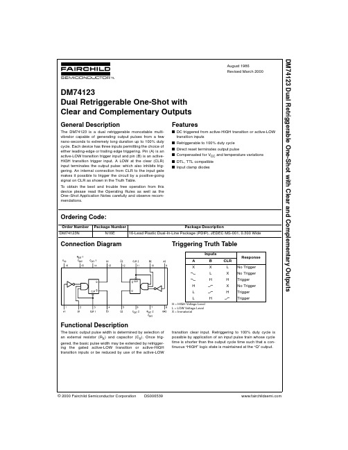
© 2000 Fairchild Semiconductor Corporation DS006539August 1986Revised March 2000DM74123 Dual Retriggerable One-Shot with Clear and Complementary OutputsDM74123Dual Retriggerable One-Shot with Clear and Complementary OutputsGeneral DescriptionThe DM74123 is a dual retriggerable monostable multi-vibrator capable of generating output pulses from a few nano-seconds to extremely long duration up to 100% duty cycle. Each device has three inputs permitting the choice of either leading-edge or trailing edge triggering. Pin (A) is an active-LOW transition trigger input and pin (B) is an active-HIGH transition trigger input. A LOW at the clear (CLR)input terminates the output pulse: which also inhibits trig-gering. An internal connection from CLR to the input gate makes it possible to trigger the circuit by a positive-going signal on CLR as shown in the Truth Table.To obtain the best and trouble free operation from this device please read the Operating Rules as well as the One–Shot Application Notes carefully and observe recom-mendations.Featuress DC triggered from active-HIGH transition or active-LOW transition inputs s Retriggerable to 100% duty cycles Direct reset terminates output pulses Compensated for V CC and temperature variations s DTL, TTL compatible s Input clamp diodesOrdering Code:Connection Diagram Triggering Truth TableH = HIGH Voltage Level L = LOW Voltage Level X = ImmaterialFunctional DescriptionThe basic output pulse width is determined by selection of an external resistor (R X ) and capacitor (C X ). Once trig-gered, the basic pulse width may be extended by retrigger-ing the gated active-LOW transition or active-HIGH transition inputs or be reduced by use of the active-LOWtransition clear input. Retriggering to 100% duty cycle is possible by application of an input pulse train whose cycle time is shorter than the output cycle time such that a con-tinuous “HIGH” logic state is maintained at the “Q” output.Order Number Package NumberPackage DescriptionDM74123NN16E16-Lead Plastic Dual-In-Line Package (PDIP), JEDEC MS-001, 0.300 WideInputsResponse A B CLR XX L No Trigger L X No Trigger HH Trigger H X No Trigger L HTrigger LHTrigger 2D M 74123Operating Rules1.An external resistor (R X ) and external capacitor (C X )are required for proper operation. The value of C X may vary from 0 to any necessary value. For small time con-stants high-grade mica, glass, polypropylene, polycar-bonate, or polystyrene material capacitors may be used. For large time constants use tantalum or special aluminum capacitors. If the timing capacitors have leakages approaching 100 nA or if stray capacitance from either terminal to ground is greater than 50 pF the timing equations may not represent the pulse width the device generates.2. When an electrolytic capacitor is used for C X a switch-ing diode is often required for standard TTL one-shots to prevent high inverse leakage current (Figure 1).However, its use in general is not recommended with retriggerable operation.3. The output pulse width (T W ) for C X > 1000 pF isdefined as follows:T W = K R X C X (1 + 0.7/R X )1.where: [R X is in Kilo-ohm][C X is in pico Farad][T W is in nano second][K ≈ 0.28]FIGURE 1.4. For C X < 1000 pF see Figure 2 for T W vs. C Xfamily curves with R X as a parameter:Pulse Width vs. R X and C XFIGURE 2.5.To obtain variable pulse width by remote trim-ming, the following circuit is recommended:Note: “R remote ” should be as close to the one-shot as possible.FIGURE 3.6.The retriggerable pulse width is calculated as shown below:T = T W + t PLH = K × R X × C X + t PLHThe retriggered pulse width is equal to the pulse width plus a delay time period (Figure 4).FIGURE 4.7.Under any operating condition C X and R X must be kept as close to the one-shot device pins as possible to minimize stray capaci-tance, to reduce noise pick-up, and to reduce I × R and Ldi/dt voltage developed along their connecting paths. If the lead length from C X to pins (6) and (7) or pins (14) and (15) is greater than 3 cm, for example, the output pulse width might be quite different from values predicted from the appropriate equations. A non-induc-tive and low capacitive path is necessary to ensure complete discharge of C X in each cycle of its operation so that the output pulse width will be accurate.8. V CC and ground wiring should conform togood high-frequency standards and practices so that switching transients on the V CC and ground return leads do not cause interaction between one-shots. A 0.01 µF to 0.10µF bypass capacitor (disk ceramic or monolithic type) from V CC to ground is necessary on each device. Furthermore, the bypass capaci-tor should be located as close to the V CC pin as space permits.Note: For further detailed device characteristics and output performance please refer to the One-Shot Application Note, AN-366.DM74123Absolute Maximum Ratings (Note 1)Note 1: The “Absolute Maximum Ratings” are those values beyond which the safety of the device cannot be guaranteed. The device should not be operated at these limits. The parametric values defined in the Electrical Characteristics tables are not guaranteed at the absolute maximum ratings.The “Recommended Operating Conditions” table will define the conditions for actual device operation.Recommended Operating ConditionsNote 2: T A = 25°C and V CC = 5V.Electrical Characteristicsover recommended operating free air temperature range (unless otherwise noted)Note 3: All typicals are at V CC = 5V, T A = 25°C.Note 4: Not more than one output should be shorted at a time.Note 5: Quiescent I CC is measured (after clearing) with 2.4V applied to all clear and A inputs, B inputs grounded, all outputs OPEN, C EXT = 0.02 µF, and R EXT = 25K Ω.Note 6: I CC is measured in the triggered state with 2.4V applied to all clear and B inputs, A inputs grounded, all outputs OPEN, C EXT = 0.02 µF, and R EXT = 25 k Ω.Supply Voltage 7V Input Voltage5.5VOperating Free Air Temperature Range 0°C to +70°C Storage Temperature−65°C to +150°CSymbol Parameter Min Nom Max Units V CC Supply Voltage4.7555.25V V IH HIGH Level Input Voltage 2V V IL LOW Level Input Voltage 0.8V I OH HIGH Level Output Current −0.8mA I OL LOW Level Output Current 16mA t WPulse Width A or B HIGH 40(Note 2)A orB LOW 40nsClear LOW 40T WQ Minimum Width of A or B65ns (Min)Pulse at Q (Note 2)R EXT External Timing Resistor 550k ΩC EXT External Timing Capacitance No RestrictionµF C WIRE Wiring Capacitance50pF at R EXT /C EXT Terminal (Note 2)T AFree Air Operating Temperature70°CSymbol ParameterConditionsMinTyp Max Units (Note 3)V I Input Clamp Voltage V CC = Min, I I = −12 mA −1.5V V OH HIGH Level V CC = Min, I OH = Max 2.53.4V Output Voltage V IL = Max, V IH = Min V OL LOW Level V CC = Min, I OL = Max 0.20.4V Output Voltage V IH = Min, V IL = Max I I Input Current @ Max Input Voltage V CC = Max, V I = 5.5V1mA I IH HIGH Level V CC = Max Data 40µA Input Current V I = 2.4VClear 80I IL Low Level V CC = Max, V I = 0.4VClear −3.2mA Input CurrentData−1.6I OS Short Circuit Output Current V CC = Max (Note 4)−10−40mA I CCSupply CurrentV CC = Max (Note 5)(Note 6)4666mA 4D M 74123Switching Characteristicsat V CC = 5V and T A = 25°CNote 7: C ECT = 1000 pF, R EXT = 10 k ΩSymbolParameterC L = 15 pF, R L = 400ΩUnitsFrom (Input)C EXT = 1000 pF, R EXT = 10 K ΩTo (Output)MinMax t PLH Propagation Delay Time A to Q 33ns LOW-to-HIGH Level Output t PLH Propagation Delay Time B to Q 28ns LOW-to-HIGH Level Output t PHL Propagation Delay Time A to Q 40ns HIGH-to-LOW Level Output t PHL Propagation Delay Time B to Q 36ns HIGH-to-LOW Level Output t PLH Propagation Delay Time Clear to Q 40ns LOW-to-HIGH Level Output t PHL Propagation Delay Time Clear to Q 27ns HIGH-to-LOW Level Output t W(out)Output Pulse Width A or B to Q3.083.76µs(Note 7)Physical Dimensions inches (millimeters) unless otherwise noted16-Lead Plastic Dual-In-Line Package (PDIP), JEDEC MS-001, 0.300 WidePackage Number N16EFairchild does not assume any responsibility for use of any circuitry described, no circuit patent licenses are implied and Fairchild reserves the right at any time without notice to change said circuitry and specifications.LIFE SUPPORT POLICYFAIRCHILD’S PRODUCTS ARE NOT AUTHORIZED FOR USE AS CRITICAL COMPONENTS IN LIFE SUPPORT DEVICES OR SYSTEMS WITHOUT THE EXPRESS WRITTEN APPROVAL OF THE PRESIDENT OF FAIRCHILD SEMICONDUCTOR CORPORATION. As used herein:1.Life support devices or systems are devices or systemswhich, (a) are intended for surgical implant into the body, or (b) support or sustain life, and (c) whose failure to perform when properly used in accordance with instructions for use provided in the labeling, can be rea-sonably expected to result in a significant injury to the user.2. A critical component in any component of a life supportdevice or system whose failure to perform can be rea-sonably expected to cause the failure of the life supportdevice or system, or to affect its safety or effectiveness. DM74123 Dual Retriggerable One-Shot with Clear and Complementary Outputs。
MEMORY存储芯片TMS320DM6437ZWT4中文规格书
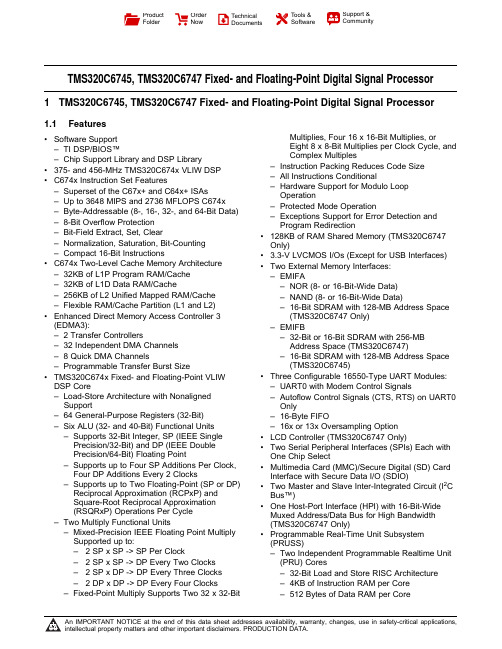
ProductFolder OrderNowTechnicalDocumentsTools &SoftwareSupport &CommunityTMS320C6745,TMS320C6747Fixed-and Floating-Point Digital Signal Processor 1TMS320C6745,TMS320C6747Fixed-and Floating-Point Digital Signal Processor 1.1Features•Software Support–TI DSP/BIOS™–Chip Support Library and DSP Library•375-and456-MHz TMS320C674x VLIW DSP•C674x Instruction Set Features–Superset of the C67x+and C64x+ISAs–Up to3648MIPS and2736MFLOPS C674x–Byte-Addressable(8-,16-,32-,and64-Bit Data)–8-Bit Overflow Protection–Bit-Field Extract,Set,Clear–Normalization,Saturation,Bit-Counting–Compact16-Bit Instructions•C674x Two-Level Cache Memory Architecture –32KB of L1P Program RAM/Cache–32KB of L1D Data RAM/Cache–256KB of L2Unified Mapped RAM/Cache–Flexible RAM/Cache Partition(L1and L2)•Enhanced Direct Memory Access Controller3 (EDMA3):–2Transfer Controllers–32Independent DMA Channels–8Quick DMA Channels–Programmable Transfer Burst Size•TMS320C674x Fixed-and Floating-Point VLIW DSP Core–Load-Store Architecture with Nonaligned Support–64General-Purpose Registers(32-Bit)–Six ALU(32-and40-Bit)Functional Units –Supports32-Bit Integer,SP(IEEE Single Precision/32-Bit)and DP(IEEE DoublePrecision/64-Bit)Floating Point–Supports up to Four SP Additions Per Clock, Four DP Additions Every2Clocks–Supports up to Two Floating-Point(SP or DP) Reciprocal Approximation(RCPxP)andSquare-Root Reciprocal Approximation(RSQRxP)Operations Per Cycle–Two Multiply Functional Units–Mixed-Precision IEEE Floating Point Multiply Supported up to:–2SP x SP->SP Per Clock–2SP x SP->DP Every Two Clocks–2SP x DP->DP Every Three Clocks–2DP x DP->DP Every Four Clocks –Fixed-Point Multiply Supports Two32x32-BitMultiplies,Four16x16-Bit Multiplies,orEight8x8-Bit Multiplies per Clock Cycle,andComplex Multiples–Instruction Packing Reduces Code Size–All Instructions Conditional–Hardware Support for Modulo LoopOperation–Protected Mode Operation–Exceptions Support for Error Detection and Program Redirection•128KB of RAM Shared Memory(TMS320C6747 Only)• 3.3-V LVCMOS I/Os(Except for USB Interfaces)•Two External Memory Interfaces:–EMIFA–NOR(8-or16-Bit-Wide Data)–NAND(8-or16-Bit-Wide Data)–16-Bit SDRAM with128-MB Address Space (TMS320C6747Only)–EMIFB–32-Bit or16-Bit SDRAM with256-MBAddress Space(TMS320C6747)–16-Bit SDRAM with128-MB Address Space (TMS320C6745)•Three Configurable16550-Type UART Modules:–UART0with Modem Control Signals–Autoflow Control Signals(CTS,RTS)on UART0 Only–16-Byte FIFO–16x or13x Oversampling Option•LCD Controller(TMS320C6747Only)•Two Serial Peripheral Interfaces(SPIs)Each with One Chip Select•Multimedia Card(MMC)/Secure Digital(SD)Card Interface with Secure Data I/O(SDIO)•Two Master and Slave Inter-Integrated Circuit(I2C Bus™)•One Host-Port Interface(HPI)with16-Bit-Wide Muxed Address/Data Bus for High Bandwidth(TMS320C6747Only)•Programmable Real-Time Unit Subsystem (PRUSS)–Two Independent Programmable Realtime Unit (PRU)Cores–32-Bit Load and Store RISC Architecture–4KB of Instruction RAM per Core–512Bytes of Data RAM per Core3TMS320C6745,TMS320C6747SPRS377F –SEPTEMBER 2008–REVISED JUNE 2014Submit Documentation FeedbackProduct Folder Links:TMS320C6745TMS320C6747TMS320C6745,TMS320C6747Fixed-and Floating-Point Digital Signal Processor Copyright ©2008–2014,Texas Instruments Incorporated The peripheral set includes:a 10/100Mbps Ethernet MAC (EMAC)with a management data input/output (MDIO)module;two I 2C Bus interfaces;3multichannel audio serial ports (McASPs)with 16/9serializers and FIFO buffers;two 64-bit general-purpose timers each configurable (one configurable as watchdog);a configurable 16-bit host-port interface (HPI)[TMS320C6747only];up to 8banks of 16pins of general-purpose input/output (GPIO)with programmable interrupt/event generation modes,multiplexed with other peripherals;3UART interfaces (one with both RTS and CTS);three enhanced high-resolution pulse width modulator (eHRPWM)peripherals;three 32-bit enhanced capture (eCAP)module peripherals which can be configured as 3capture inputs or 3auxiliary pulse width modulator (APWM)outputs;two 32-bit enhanced quadrature encoded pulse (eQEP)peripherals;and 2external memory interfaces:an asynchronous and SDRAM external memory interface (EMIFA)for slower memories or peripherals,and a higher speed memory interface (EMIFB)for SDRAM.The Ethernet Media Access Controller (EMAC)provides an efficient interface between the TMS320C6745/6747device and the network.The EMAC supports both 10Base-T and 100Base-TX,or 10Mbps and 100Mbps in either half-or full-duplex mode.Additionally,an MDIO interface is available for PHY configuration.The rich peripheral set provides the ability to control external peripheral devices and communicate with external processors.For details on each of the peripherals,see the related sections later in this document and the associated peripheral reference guides.(1)For more information on these devices,see Section 8,Mechanical Packaging and OrderableInformation.Device Information (1)PART NUMBERPACKAGE BODY SIZE TMS320C6745HLQFP (176)24.00mm x 24.00mm TMS320C6747BGA (256)17.00mm x 17.00mm。
proteus元件名称对照表
元件名称中英文名说明7407 驱动门1N914 二极管74Ls00 与非门74LS04 非门74LS08 与门74LS390 TTL 双十进制计数器7SEG 4针BCD-LED 输出从0-9 对应于4根线的BCD码7SEG 3-8译码器电路BCD-7SEG转换电路ALTERNATOR 交流发电机AMMETER-MILLI mA安培计AND 与门BATTERY 电池/电池组BUS 总线CAP 电容***CAPACITOR 电容器CLOCK 时钟信号源***CRYSTAL 晶振D-FLIPFLOP D触发器FUSE 保险丝GROUND 地LAMP 灯LED-RED 红色发光二极管LM016L 2行16列液晶可显示2行16列英文字符,有8位数据总线D0-D7,RS,R/W,EN三个控制端口(共14线),工作电压为5V。
没背光,和常用的1602B功能和引脚一样(除了调背光的二个线脚)LOGIC ANALYSER 逻辑分析器LOGICPROBE 逻辑探针LOGICPROBE[BIG] 逻辑探针用来显示连接位置的逻辑状态LOGICSTATE 逻辑状态用鼠标点击,可改变该方框连接位置的逻辑状态LOGICTOGGLE 逻辑触发MASTERSWITCH 按钮手动闭合,立即自动打开***MOTOR 马达OR 或门POT-LIN 三引线可变电阻器POWER 电源***RES 电阻RESISTOR 电阻器SWITCH 按钮手动按一下一个状态SW-SPDT-mom 二选通一按钮***触发开关BUTTONVOLTMETER 伏特计VOLTMETER-MILLI mV伏特计VTERM 串行口终端***Electromechanical 电机Inductors 变压器Laplace Primitives 拉普拉斯变换Memory IcsMicroprocessor IcsMiscellaneous 各种器件 AERIAL-天线;ATAHDD;ATMEGA64;BATTERY;CELL;CRYSTAL-晶振;FUSE;METER-仪表;Modelling Primitives 各种仿真器件是典型的基本元器模拟,不表示具体型号,只用于仿真,没有PCBOptoelectronics 各种发光器件发光二极管,LED,液晶等等PLDs & FPGAsResistors 各种电阻Simulator Primitives 常用的器件Speakers & SoundersSwitches & Relays 开关,继电器,键盘BUTTON 触发开关Switching Devices 晶阊管Transistors 晶体管(三极管,场效应管)TTL 74 seriesTTL 74ALS seriesTTL 74AS seriesTTL 74F seriesTTL 74HC seriesTTL 74HCT seriesTTL 74LS seriesTTL 74S seriesAnalog Ics 模拟电路集成芯片Capacitors 电容集合CMOS 4000 seriesConnectors 排座,排插Data Converters ADC,DACDebugging Tools 调试工具***7SEG 数码管ECL 10000 Series 各种常用集成电路1.电阻固定电阻:RES半导体电阻:RESSEMT电位计;POT变电阻;RVAR可调电阻;res1可变电阻 pot2.电容定值无极性电容;CAP定值有极性电容;CAP半导体电容:CAPSEMI可调电容:CAPVAR3.电感:INDUCTOR4.二极管:发光二极管:LED5.三极管 :NPN16.结型场效应管:场效应管场效应管9.继电器:PELAY. LIB10.灯泡:LAMP11.运放:OPAMP12.数码管: 7-SEG_DP (MISCELLANEOUS13.开关;sw_pb原理图常用库文件:MiscellaneousDallasIntelProtel DOS SchematicPCB元件常用库:General部分分立元件库元件名称及中英对照AND 与门ANTENNA 天线BATTERY 直流电源BELL 铃,钟BVC 同轴电缆接插件BRIDEG 1 整流桥(二极管) BRIDEG 2 整流桥(集成块) BUFFER 缓冲器BUZZER 蜂鸣器CAP 电容CAPACITOR 电容CAPACITOR POL 有极性电容CAPVAR 可调电容CIRCUIT BREAKER 熔断丝COAX 同轴电缆CON 插口CRYSTAL 晶体整荡器DB 并行插口DIODE 二极管DIODE SCHOTTKY 稳压二极管DIODE VARACTOR 变容二极管DPY_3-SEG 3段LEDDPY_7-SEG 7段LEDDPY_7-SEG_DP 7段LED(带小数点) ELECTRO电解电容FUSE 熔断器INDUCTOR 电感INDUCTOR IRON 带铁芯电感INDUCTOR3 可调电感JFET N N沟道场效应管JFET P P沟道场效应管LAMP 灯泡LAMP NEDN 起辉器LED 发光二极管METER 仪表MICROPHONE 麦克风MOSFET MOS管MOTOR AC 交流电机MOTOR SERVO 伺服电机NAND 与非门NOR 或非门NOT 非门NPN NPN三极管NPN-PHOTO 感光三极管OPAMP 运放OR 或门PHOTO 感光二极管PNP 三极管NPN DAR NPN三极管PNP DAR PNP三极管POT 滑线变阻器PELAY-DPDT 双刀双掷继电器RES1.2 电阻可变电阻RESISTOR BRIDGE 桥式电阻RESPACK 电阻SCR 晶闸管PLUG 插头PLUG AC FEMALE 三相交流插头SOCKET 插座SOURCE CURRENT 电流源SOURCE VOLTAGE 电压源SPEAKER扬声器SW 开关SW-DPDY 双刀双掷开关SW-SPST 单刀单掷开关SW-PB 按钮THERMISTOR 电热调节器TRANS1 变压器TRANS2 可调变压器TRIAC 三端双向可控硅TRIODE 三极真空管VARISTOR 变阻器ZENER 齐纳二极管DPY_7-SEG_DP 数码管SW-PB 开关其他元件库Protel Dos Schematic 4000 Cmos .Lib (40.系列CMOS管集成块元件库)4013 D 触发器4027 JK 触发器Protel Dos Schematic Analog (模拟数字式集成块元件库)AD系列 DAC系列 HD系列 MC系列Protel Dos Schematic (比较放大器元件库)Protel Dos Shcematic (INTEL公司生产的80系列CPU集成块元件库)Protel Dos Schematic (线性元件库)例555Protel Dos Schemattic Memory (内存存储器元件库)Protel Dos Schematic (SY系列集成块元件库)Protes Dos Schematic (摩托罗拉公司生产的元件库)Protes Dos Schematic (NEC公司生产的集成块元件库)Protes Dos Schematic Operationel (运算放大器元件库)Protes Dos Schematic (晶体管集成块元件库 74系列)Protel Dos Schematic Voltage (电压调整集成块元件库)Protes Dos Schematic (齐格格公司生产的Z80系列CPU集成块元件库)元件属性对话框中英文对照Lib ref 元件名称Footprint 器件封装Designator 元件称号Part 器件类别或标示值Schematic Tools 主工具栏Writing Tools 连线工具栏Drawing Tools 绘图工具栏稳压二极管 ZENER DIODE肖特基二极管 SCHOTTKY DIODE二极管 DIODE变容二极管 VARIODE三极管 TRANSISTOR电感 INDUCTOR磁环 EMIFIL电阻 RESISTOR电容 CAPACITY晶振 CRYSTAL涤纶电容 MYLAR CAP电解电容 ELECT CAP瓷片电容 CERAMIC CAP安规电容 FILM CAPProtel 99 se的元件中英文PcbRe: [分享] protel99se 元件名系表--分立元件库中英文对照电阻 AXIAL 无极性电容 RAD 电解电容 RB- 电位器 VR 二极管 DIODE 三极管 TO 电源稳压块78和79系列 TO-126H和TO-126V 场效应管和三极管一样整流桥 D-44 D-37 D-46 单排多针插座 CON SIP 双列直插元件 DIP 晶振 XTAL1电阻:RES1,RES2,RES3,RES4;封装属性为axial系列无极性电容:cap;封装属性为到电解电容:electroi;封装属性为.4到电位器:pot1,pot2;封装属性为vr-1到vr-5二极管:封装属性为(小功率)(大功率)三极管:常见的封装属性为to-18(普通三极管)to-22(大功率三极管)to-3(大功率达林顿管)电源稳压块有78和79系列;78系列如7805,7812,7820等79系列有7905,7912,7920等常见的封装属性有to126h和to126v整流桥:BRIDGE1,BRIDGE2: 封装属性为D系列(D-44,D-37,D-46)电阻:其中指电阻的长度,一般用瓷片电容:。
proteus元件对照表(经典详细)之欧阳语创编

proteus常用元件中英文对照表元件名称中文名说明7407 驱动门 1N914 二极管74Ls00 与非门 74LS04 非门74LS08 与门 74LS390 TTL 双十进制计数器 7SEG 4针BCD-LED 输出从0-9 对应于4根线的BCD码 7SEG 3-8译码器电路BCD-7SEG转换电路ALTERNATOR 交流发电机AMMETER-MILLI mA安培计AND 与门 BATTERY 电池/电池组 BUS 总线 CAP 电容CAPACITOR 电容器 CLOCK 时钟信号源 CRYSTAL 晶振 D-FLIPFLOP D触发器 FUSE 保险丝 GROUND 地 LAMP 灯 LED-RED 红色发光二极管 LM016L 2行16列液晶可显示2行16列英文字符,有8位数据总线D0-D7,RS,R/W,EN三个控制端口(共14线),工作电压为5V。
没背光,和常用的1602B 功能和引脚一样(除了调背光的二个线脚) LOGIC ANALYSER 逻辑分析器 LOGICPROBE 逻辑探针 LOGICPROBE[BIG] 逻辑探针用来显示连接位置的逻辑状态LOGICSTATE 逻辑状态用鼠标点击,可改变该方框连接位置的逻辑状态 LOGICTOGGLE 逻辑触发 MASTERSWITCH 按钮手动闭合,立即自动打开 MOTOR 马达 OR 或门 POT-LIN 三引线可变电阻器 POWER 电源 RES 电阻 RESISTOR 电阻器 SWITCH 按钮手动按一下一个状态SWITCH-SPDT 二选通一按钮VOLTMETER 伏特计VOLTMETER-MILLI mV伏特计VTERM 串行口终端Electromechanical 电机Inductors 变压器 Laplace Primitives 拉普拉斯变换Memory Ics Microprocessor Ics Miscellaneous 各种器件AERIAL-天线;ATAHDD;ATMEGA64;BATTERY;CELL;CRYSTAL-晶振;FUSE;METER-仪表;Modelling Primitives 各种仿真器件是典型的基本元器模拟,不表示具体型号,只用于仿真,没有PCB Optoelectronics 各种发光器件发光二极管,LED,液晶等等 PLDs &FPGAs Resistors 各种电阻Simulator Primitives 常用的器件 Speakers & Sounders Switches & Relays 开关,继电器,键盘 Switching Devices 晶阊管 Transistors 晶体管(三极管,场效应管) TTL 74 series TTL 74ALSseries TTL 74AS series TTL 74F series TTL 74HC series TTL 74HCTseries TTL 74LS series TTL 74S series Analog Ics 模拟电路集成芯片 Capacitors 电容集Device.lib 包括电阻、电容、二极管、三极管和PCB的连接器符号ACTIVE.LIB 包括虚拟仪器和有源器件DIODE.LIB 包括二极管和整流桥DISPLAY.LIB 包括LCD、LEDBIPOLAR.LIB 包括三极管FET.LIB 包括场效应管ASIMMDLS.LIB 包括模拟元器件VALVES .LIB 包括电子管ANALOG.LIB 包括电源调节器、运放和数据采样ICCAPACITORS.LIB 包括电容COMS.LIB 包括 4000系列ECL.LIB 包括ECL10000系列MICRO.LIB 包括通用微处理器OPAMP.LIB 包括运算放大器RESISTORS.LIB 包括电阻FAIRCHLD .LIB 包括FAIRCHLD 半导体公司的分立器件LINTEC.LIB 包括 LINTEC公司的运算放大器NATDAC.LIB 包括国家半导体公司的数字采样器件NATOA.LIB 包括国家半导体公司的运算放大器TECOOR.LIB 包括TECOOR公司的 SCR 和TRIACTEXOAC.LIB 包括德州仪器公司的运算放大器和比较器ZETEX .LIB 包括ZETEX 公司的分立器件分立元件库元件名称及中英对照AND 与门ANTENNA 天线BATTERY 直流电源BELL 铃,钟BVC 同轴电缆接插件BRIDEG 1 整流桥(二极管) BRIDEG 2 整流桥(集成块) BUFFER 缓冲器BUZZER 蜂鸣器CAP 电容CAPACITOR 电容CAPACITOR POL 有极性电容CAPVAR 可调电容CIRCUIT BREAKER 熔断丝COAX 同轴电缆CON 插口CRYSTAL 晶体整荡器DB 并行插口DIODE 二极管DIODE SCHOTTKY 稳压二极管DIODE VARACTOR 变容二极管DPY_3-SEG 3段LED DPY_7-SEG 7段LED DPY_7-SEG_DP 7段LED(带小数点) ELECTRO 电解电容FUSE 熔断器INDUCTOR 电感INDUCTOR IRON 带铁芯电感INDUCTOR3 可调电感 JFET N N沟道场效应管JFET P P沟道场效应管 LAMP 灯泡LAMP NEDN 起辉器LED 发光二极管METER 仪表MICROPHONE 麦克风MOSFET MOS管MOTOR AC 交流电机MOTOR SERVO 伺服电机NAND 与非门NOR 或非门NOT 非门 NPN NPN 三极管 NPN-PHOTO 感光三极管OPAMP 运放OR 或门PHOTO 感光二极管PNP 三极管 NPNDAR NPN三极管 PNP DAR PNP三极管POT 滑线变阻器PELAY-DPDT 双刀双掷继电器 RES1.2 电阻RES3.4 可变电阻RESISTOR BRIDGE ? 桥式电阻RESPACK ? 电阻SCR 晶闸管PLUG ? 插头 PLUG AC FEMALE 三相交流插头SOCKET ? 插座SOURCE CURRENT 电流源SOURCE VOLTAGE 电压源SPEAKER 扬声器SW ? 开关 SW-DPDY ? 双刀双掷开关SW-SPST ? 单刀单掷开关 SW-PB 按钮THERMISTOR 电热调节器TRANS1 变压器TRANS2 可调变压器TRIAC ? 三端双向可控硅 TRIODE ? 三极真空管 VARISTOR 变阻器ZENER ? 齐纳二极管DPY_7-SEG_DP 数码管 SW-PB 开关元件名称中文名说明 7407 驱动门1N914 二极管74Ls00 与非门 74LS04 非门74LS08 与门 74LS390 TTL 双十进制计数器 7SEG 4针BCD-LED 输出从0-9 对应于4根线的BCD码 7SEG 3-8译码器电路BCD-7SEG转换电路 ALTERNATOR 交流发电机AMMETER-MILLI mA安培计 AND 与门BATTERY 电池/电池组 BUS 总线CAP 电容 CAPACITOR 电容器CLOCK 时钟信号源 CRYSTAL 晶振 D-FLIPFLOP D触发器 FUSE 保险丝GROUND 地 LAMP 灯 LED-RED 红色发光二极管 LM016L 2行16列液晶可显示2行16列英文字符,有8位数据总线D0-D7, RS,R/W,EN三个控制端口(共14线),工作电压为5V。
DM74LS154N中文资料
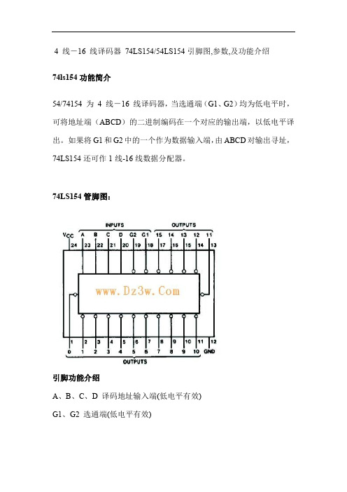
4 线-16 线译码器74LS154/54LS154引脚图,参数,及功能介绍74ls154功能简介54/74154 为4 线-16 线译码器,当选通端(G1、G2)均为低电平时,可将地址端(ABCD)的二进制编码在一个对应的输出端,以低电平译出。
如果将G1和G2中的一个作为数据输入端,由ABCD对输出寻址,74LS154还可作1线-16线数据分配器。
74LS154管脚图:引脚功能介绍A、B、C、D 译码地址输入端(低电平有效)G1、G2 选通端(低电平有效)0-15 输出端(低电平有效) 74ls154真值表:推荐工作条件74ls154电气参数极限值电源电压: 7V输入电压: 5.5V工作环境温度54154:-55~125℃74154:0~70℃贮存温度:-65~150℃线译码器74LS154引脚,参数,及功能介绍--------------------------------------------------------------------------------4 线-16 线译码器74LS154/54LS154引脚图,参数,及功能介绍74ls154功能简介:54/74154 为4 线-16 线译码器,当选通端(G1、G2)均为低电平时,可将地址端(ABCD)的二进制编码在一个对应的输出端,以低电平译出。
如果将G1和G2中的一个作为数据输入端,由ABCD对输出寻址,74LS154还可作1线-16线数据分配器。
74LS154管脚图:引脚功能介绍A、B、C、D 译码地址输入端(低电平有效)G1、G2 选通端(低电平有效)0-15 输出端(低电平有效)74ls154真值表:推荐工作条件74ls154电气参数极限值电源电压: 7V输入电压: 5.5V工作环境温度54154:-55~125℃74154:0~70℃贮存温度:-65~150℃本文来自: 原文网址:/info/commonIC/0075219.html本文来自: 原文网址:/info/commonIC/0075219.html74ls154芯片资料2007-08-20 20:4874ls138译码器74ls139 跟74ls138类似,区别在于139内部是2个独立的2-4译码器。
常用集成电路的型号和功能说明解读

常用集成电路的型号和功能说明型号功能资料ACP2371NI 多制式数字音频信号处理电路ACVP2205 梳状滤波、视频信号处理电路AN5071 波段转换控制电路AN5195K 子图像信号处理电路AN5265 伴音功率放大电路AN5274 伴音功率放大电路AN5285K 伴音前置放大电路AN5342K 图像水平轮廓校正、扫描速度调制电路AN5348K AI信号处理电路AN5521 场扫描输出电路AN5551 枕形失真校正电路AN5560 50/60Hz场频自动识别电路AN5612 色差、基色信号变换电路AN5836 双声道前置放大及控制电路AN5858K TV/AV切换电路AN5862K(AN5862S) 视频模拟开关AN5891K 音频信号处理电路AT24C02 2线电可擦、可编程只读存储器AT24C04 2线电可擦、可编程只读存储器AT24C08 2线电可擦、可编程只读存储器ATQ203 扬声器切换继电器电路BA3880S 高分辨率音频信号处理电路BA3884S 高分辨率音频信号处理电路BA4558N 双运算放大器BA7604N 梳状切换开关电路BU9252S 8bitA/D转换电路CAT24C16 2线电可擦、可编程只读存储器CCU-FDTV 微处理器CCU-FDTV-06 微处理器CD54573A/CD54573CS 波段转换控制电路CH0403-5H61 微处理器CH04801-5F43 微处理器CH05001(PCA84C841) 微处理器CH05002 微处理器CH7001C 数字NTSC/PAL编码电路CHT0406 微处理器CHT0803(TMP87CP38N*) 8bit微处理器CHT0807(TMP87CP38N) 8bit微处理器CHT0808(TMP87CP38N) 8bit微处理器CHT0818 微处理器CKP1003C 微处理器CKP1004S(TMP87CK38N) 微处理器CKP1006S(TMP87CH38N) 微处理器CKP1008S(TMP87CK38N/F) 微处理器CKP1009S(TMP87CH38N) 微处理器CKP1105S(Z90231) 微处理器CKP1301S(TMP87CH38N) 微处理器CKP1403S 微处理器CM0006CF 数字会聚校正电路CNX62A 光电耦合器CNX82A 光电耦合器CPF8598 存储器CTV222S.PRC1.2 微处理器CTV225S-PRC1 微处理器CTV591S.GW3 微处理器CXA1545AS TV/AV多路切换电路CXA1642P 背景歌声消除电路CXA1686M 时钟信号发生器CXA1779P 基色信号处理电路CXP1103S-9919EP 微处理器CXP750096 微处理器CXP85332-108A 微处理器DM8361 单片集成TV小信号处理电路DPU2553/DPU2554 偏转信号处理电路DTI2251 数字色信号过渡特性改善电路GAL16V8C 同步信号变换电路GD74LS10 三组3输入与非门GD74LS393 双4位二进制计数器GD74LS74A 双D触发器GM99200B 微处理器HA11508 图像及伴音信号转换控制电路HCF4046B 低功耗通用锁相环电路HCF4052B 双4选1模拟开关HCF4053BE 三组2路模拟开关HCT157 VGA信号与TV/AV同步信号切换电路HCT4046AD 低功耗通用锁相环电路HD14066 四组双向模拟开关HD14066B 四组双向模拟开关HD14066BP 四组双向模拟开关HEF4052 双4选1模拟开关HEF4053 三组2路模拟开关HEF4094 8级移位-存储总线寄存器HIC1015 开关电源稳压控制及保护电路HIC1016 开关电源稳压控制及保护电路HIC1026 保护模块HM4864P-12 随机存取存储器HPD6325C D/A转换电路HS0038 遥控信号接收电路IX0823GE 微处理器IX1763CEN1 单片集成TV小信号处理电路JLC1562BF 总线控制输入/输出口扩展电路K6274K/D 图像中频带通滤波器K9450M 伴音第一中频带通滤波器KA2107 音频控制电路KA2500 宽带视频放大电路KA3S0680R 开关电源专用厚膜电路KA3S0880RFB 开关电源专用厚膜电路KA7630 多路稳压输出电路KB2511B 数字偏转电路KONKA266(P83C266) 微处理器KS88C3216 微处理器KS88C8324 微处理器L7805 5V固定正稳压器L7808 8V固定正稳压器L7812 12V固定正稳压器L78LR05/L78LR05D/L78LR50-MA/L78M05F/L78M05FA/L78MR05/L78MR05FA 5V稳压复位电路L78OSO5FA 5V可控稳压电路L7912 9V固定负稳压器L7918 18V固定负稳压器LA2785 杜比逻辑处理电路LA4225 5W音频功率放大电路LA4261 立体声功率放大电路LA4270 6W×2音频功率放大电路LA4280 10W×2音频功率放大电路LA4282 10W×2音频功率放大电路LA4445 双声道音频功率放大电路LA6358 双运算放大器LA7016 电子开关LA7210 同步检测电路LA7222 二回路、二接点电子开关LA7406 画中画接口电路LA7575 图像中频放大电路LA76810 TV小信号处理电路LA76832N TV小信号处理电路LA7685 中频及图像信号处理电路LA7838 场扫描电路LA7840 场扫描输出电路LA7841 场扫描输出电路LA7845 场扫描输出电路LA7845N 场扫描输出电路LA7846N 场扫描输出电路LA7910 波段转换控制电路LA7950 场频识别控制电路LA7954 视频转换电路LC344250Z 多端动态存储器LC74401E 画中画(PIP)控制电路LC78815M 双通道16bitD/A变换电路LC863316A 微处理器LC863320A 微处理器LC863328A 微处理器LC863348A 微处理器LC864512 微处理器LC864512V-5D18 微处理器LC864512V-5C77 微处理器LC864525 微处理器LC864916A 微处理器LM317 稳压器LM324 四运算放大器LM358 双运算放大器LM567 锁相环电路LUKS-5140-M2 微处理器LV1010N 杜比逻辑处理电路M32L1632512A 同步图形存储器M34300N-587SP 微处理器M34300N4-555SP 微处理器M37210M3-508SP 微处理器M37210M3-800SP 多制式数字音频信号处理电路M37210M3-902SP 微处理器M37210M4-705SP 微处理器M37211M2-609SP 微处理器M37220M3 微处理器M37221M6-065SP 微处理器M37222M6-084SP 微处理器M37225 微处理器M37270MF-168SP 微处理器M37271MP-209SP 微处理器M37274EFSP 微处理器M37280 微处理器M37551MA-0545SP 微处理器M50436-688SP 微处理器M51131L 话筒演唱及混响音量控制电路M5218AP 双运算放大器M52340SP 单片集成TV小信号处理电路M52470AP 三通道4输入模拟开关M54573L 波段转换控制电路M62354FP 六通道8bitD/A转换电路M62438FP SRSM65839SP 数字式卡拉OK信号处理电路M66312P PIP控制电路M6M80011P 存储器M6M80041P 存储器MALF24C01 存储器MALF24C02 存储器MB3110A 超低音频信号处理电路MB81461-12RS 动态随机存储器MC14066BCP 四组双向模拟开关MC141625A 梳状滤波器MC141628 前置亮、色信号分离梳状滤波器MC144110P D/A转换电路MC14577C 双视频放大电路MC33064D5 复位用欠压检测电路MC44608 开关稳压电源电压模式控制器MC68HC16R1(SC43402CFC) 微处理器MCM6206BBE 32K×8bit快速静态随机存取存储器MCU2600 时钟信号发生器MM1031XS 宽带视频放大电路MM1053XS 多路信号高速切换电路MM1113XS 多路信号高速切换电路MM1495XD A/V切换电路MN1515TWE/TWP 微处理器MN152810TTD5 微处理器MN152811TIX 微处理器MN15282 微处理器MN1871675T6S 微处理器MN1871675T7M 微处理器MN1872432TWI 微处理器MN187-681 微处理器MN3868 1H基带延迟线电路MSP3410 多制式丽音解码电路MSP3410B 多制式丽音解码电路MSP3410D 多制式丽音解码电路MSP3410D-52 多制式丽音解码电路MSP3410D-CS 多制式丽音解码电路MSP3410D-PP-B4 多制式丽音解码电路MSP3410D-P0-B4 多制式丽音解码电路MSP3415D-AI I*IC总线控制多制式音频处理电路MSP3463G 音频信号处理电路NE5532N 内部补偿低噪声双运算放大器NE/SE567 音调与频率解码、锁相环电路NE567N 音调与频率解码、锁相环电路NJM2234L 伴音声道控制开关NJM2700L WOW音频处理电路NJW1103 杜比定向逻辑和音色选择电路NJW1132AL 伴音BBE处理电路NM24C04EN 存储器NN5099K/NN5199K 单片集成多制式TV小信号处理电路NP83C266BRNA 微处理器NV320P 数字视频信号处理电路NVM3060 存储器OM8361 单片集成TV小信号处理电路OM8361-VS0469 单片集成TV小信号处理电路OM8839 I*IC总线控制单片集成TV小信号处理电路OM8839PS I*IC总线控制单片集成TV小信号处理电路OM8839PS-K9G216 I*IC总线控制单片集成TV小信号处理电路ONWA KWEC42.2ONWA KWEC44.1OTT531 +5V稳压复位电路P83C266BDR 微处理器P87C766 微处理器P87C766BDR(CKP1401S) 微处理器P87C766DT 微处理器PC74HT241P 线性驱动数据缓冲电路PC713F6 光耦合器PCA841P-177 微处理器PCA84C122/PCA84C222/PCA84C422/PCA84C622/ PCA84C822 PCA84C440P/401 微处理器PCA84C641 微处理器PCA84C840P-054 微处理器PCA8516 字符形成电路PCA8521 遥控编码发射电路PCA8521BT 遥控编码发射电路PCF8581P 存储器PCF8582 存储器PCF8589C-2 存储器PCF8594C-2 存储器PCF8598 E2PROM存储器PCF8598C-2 E2PROM存储器PCF8598E E2PROM存储器PCX8598X-2 E2PROM存储器PIP2250 PIP信号处理电路PQ05RF 受控+5V稳压器PQ09RD11(78HR09) 受控+9V稳压器PQ12RF 受控+12V稳压器PQ12RF2 受控+12V稳压器S24C08A 存储器SAA3010T 遥控信号发射电路SAA4955TJ 场存储器SAA4955TS 数字式场存储器SAA4956TJ 具有降噪功能的场存储器SAA4961 PAL/NTSC兼容梳状滤波器SAA4977H 倍场频处理电路SAA4981 单片集成16:9压缩处理电路SAA4991WP 运动估算和补偿、降低行间闪烁、变焦和降噪电路SAA5284 多媒体视频数据捕获电路SAA5700GP 汉字系统图文电视(CCST)解码电路SAA7280P 丽音信号处理电路SAA7283ZP 丽音解调解码电路SAB9077H PIP控制电路SBX1765-01 数字梳状滤波器SDA9187 PIPSDA9187-2X PIPSDA9189X 1/4屏幕多画面PIP处理电路SDA9205 三路8bitA/D转换电路SDA9220 存储同步控制电路SDA9251 存储器SDA9257 时钟同步发生器SDA9280 显示信号处理电路SDA9288 PIP/POP信号处理电路SDA9288X PIP/POP信号处理电路SDA9290 数字图像处理电路SDA9361 DDC-PLUS偏转控制电路SDA9362 扫描小信号处理电路SDA9400 扫描变换处理电路SE110N 开关电源误差信号放大电路SE116E 开关电源误差信号放大电路SE140N/SE145N 开关电源误差信号放大电路SECL810 音频信号控制电路SID2500-DOBO R、G、B混合处理电路SKW011-829A2202 微处理器SMM-201N 微处理器ST24C02 2线电可擦、可编程只读存储器ST24C04 2线电可擦、可编程只读存储器ST63156 微处理器ST6367B1/FEJ 微处理器ST92196 微处理器STK392-040 三通道会聚校正放大电路STK392-110 三通道会聚校正放大电路STR-6658B 开关电源厚膜电路STR-D1005T 开关电源厚膜电路STR-F6454 开关电源厚膜电路STR-F6653 开关电源厚膜电路STR-F6654 开关电源厚膜电路STR-F6656 开关电源厚膜电路STR-F6658B 开关电源厚膜电路STR-F6707 开关电源厚膜电路STR-G8656 开关电源厚膜电路STR-M6529F04 开关电源厚膜电路STR-M6833BF04 开关电源厚膜电路STR-S5941 开关电源厚膜电路STR-S6308 开关电源厚膜电路STR-S6309 开关电源厚膜电路STR-S6709 开关电源厚膜电路STR-S6709A 开关电源厚膜电路STR-S6709AN 开关电源厚膜电路STR-Z3202 开关电源厚膜电路STR-Z4302 开关电源厚膜电路STR-Z4479 开关电源厚膜电路STV2116 视频解码电路STV2246 I*IC总线控制单片集成TV小信号处理电路STV2248 I*IC总线控制单片集成TV小信号处理电路STV5111 R、G、B高压视频放大电路STV5112 R、G、B高压视频放大电路STV9306 场扫描输出电路STV9379 场扫描输出电路T7808CT 8V固定正稳压器TA1216AN 三通道音频信号处理电路TA1218AN AV/TV切换电路TA1219AN AV/TV切换电路TA1219N AV/TV切换电路TA1222AN 多制式视频、色度、同步、偏转信号处理电路TA1222BN 多制式视频、色度、同步、偏转信号处理电路TA1226N 亮度信号瞬态校正电路TA1229N SECAM制解码电路TA1270BF PAL/NTSC视频和色信号处理电路TA1316AN 逐行扫描倍场频画质增强电路TA1318N 多制式扫描行场振荡电路TA2009P 数字信号滤波电路TA2047N 丽音系统模拟滤波电路TA2136F/N 声音重演信号(SRS)处理电路TA24C04/TA24C08/TL24C04 2线电可擦、可编程只读存储器TA7347P S端子切换电路TA7439 三波段数字控制音频信号切换及处理电路TA7508P 四运算放大器TA75393S 双电压比较器TA75458P 双运算放大器TA7555F/P 时间延时器TA75558P 双运算放大器TA75559P 双运算放大器TA7809S 9V固定正稳压器TA78L09AP 9V固定正稳压器TA8173AP 双声道立体环绕声处理电路TA8200AH 双声道音频功率放大电路TA8211AH 双声道音频功率放大电路TA8213K 重低音功率放大电路TA8218AH 音频功率放大电路TA8256H 6W×3通道音频功率放大电路TA8256HV 三通道音频功率放大电路TA8258H 双通道音频功率放大电路TA8403K 场扫描输出电路TA8427K 场扫描输出电路TA8445K 场扫描输出电路TA8615N 制式转换电路TA8628N 带电子音量控制的AV/TV开关电路TA8659BN 多制式视频、偏转、文字显示信号处理及制式转换电路TA8710S 伴音中频转换电路TA8720AN TV/AV(S-VHS)切换电路TA8765N SECAM解码电路TA8772AN PAL/NTSC/SECAM基带1H延迟电路TA8772CN PAL/NTSC/SECAM基带1H延迟电路TA8776N 环绕声信号处理电路TA8777NFA-1 PIP画面视频信号选择开关TA8795AF PIP画面多制式亮度、色度、同步信号处理电路TA8814N 彩色瞬态特性改善电路TA8815BN 模拟视频信号选择开关TA8851AN 双极型I*IC总线控制AV开关TA8851BN 双极型I*IC总线控制AV开关TA8851CN 双极型I*IC总线控制AV开关TA8859CP 枕形失真校正电路TA8859P 枕形失真校正电路TA8880CN 视频、色度、同步信号处理电路TA8889P I*IC总线控制白平衡调整电路TAIF24C04 存储器TB1204N 丽音信号处理电路TB1212N 丽音信号处理电路TB1227AN PAL/NTSC/SECAM视频、色度、扫描小信号处理电路TB1227N PAL/NTSC/SECAM视频、色度、扫描小信号处理电路TB1227 PAL/NTSC/SECAM视频、色度、扫描小信号处理电路TB1231N 视频、色度、扫描小信号处理电路TB1238AN 视频、色度、扫描小信号处理电路TB1238N 视频、色度、扫描小信号处理电路TB1240N I*IC总线控制TV信号处理电路TB1240AN I*IC总线控制TV信号处理电路TBA2800 遥控信号接收电路TC4052 双4选1模拟开关TC4052B 双4选1模拟开关TC4052BP 双4选1模拟开关TC4053 三组2路双向模拟开关TC4053AP/TC4053BP 三组2路双向模拟开关TC4066AF 四组双向模拟开关TC4094BP 端口扩展电路TC74HC4053AP 三组2路双向模拟开关TC74HC4066AF 四组双向模拟开关TC9028F 遥控信号发射电路TC9083F/P 单片PIP控制电路TC9089 数字Y/C信号分离电路TC9090AN 多制式3行数字Y/C信号分离电路TC9090CN 多制式3行数字Y/C信号分离电路TC9090N/F 多制式3行数字Y/C信号分离电路TC9097F 彩色信号处理电路TC90A49P 多制式3行数字Y/C信号分离电路TC9415N 数字卡拉OK电路TDA1521 双通道伴音功率放大电路TDA1521A 双通道伴音功率放大电路TDA1524A 立体声(音量/音调)控制电路TDA1543 数控变换电路TDA16846 开关电源厚膜电路TDA2007 6W×2音频功率放大电路TDA2007A 6W×2音频功率放大电路TDA2009A 10W×2双路音频功率放大电路TDA2030 14WTDA2595 行、场扫描及同步脉冲发生器TDA2616 带静音功能的12W×2TDA3504 视频控制、矩阵电路TDA3654 场扫描输出电路TDA3857 准分离伴音解码电路TDA4472 TV信号前置处理电路TDA4505 彩色电视小信号处理电路TDA4555 多制式色度解码电路TDA4565 亮度延迟、彩色暂态特性改善电路TDA4601 开关电源厚膜电路TDA4605 开关电源厚膜电路TDA4605-3 开关电源厚膜电路TDA4665 基带彩色信号延迟电路TDA4671 彩色瞬态改善(CTI)电路TDA4681 矩阵变换及亮度控制电路TDA4780 视频信号处理电路TDA4853/TDA4854 I*IC总线自同步偏转控制电路TDA5112 单片视频放大输出电路TDA5330T 高频调谐器专用贴片电路TDA6101Q 视频放大输出电路TDA6103Q 视频放大输出电路TDA6107Q 视频放大输出电路TDA6108JF 单片视频放大输出电路TDA6110Q 视频放大输出电路TDA6111Q 视频放大输出电路TDA6120Q 宽带视频放大输出电路TDA6151 卫星电视接收视频处理电路TDA7056A/TDA7056B 超重低音功率放大电路TDA7057AQ 双声道音频功率放大电路TDA7265 双通道音频功率放大电路TDA7297 双声道功率放大电路TDA7429S 立体声信号切换、处理电路TDA7496 带直流音量控制的双通道音频功率放大电路TDA8133 具有“禁止”和复位功能的+5.1V、+8V稳压器TDA8139 具有CPU复位功能的稳压电路TDA8145 光栅东/西失真校正电路TDA8170 场扫描输出电路TDA8172 场扫描输出电路TDA8177F 场扫描输出电路TDA8179 场扫描输出电路TDA8219 色度信号解码电路TDA8305A 图像中放电路TDA8310 PIPTDA8310A PIP全制式色度信号处理电路TDA8341 内载波中频信号处理电路TDA8350Q 直流耦合场偏转和东/西枕校输出电路TDA8351 场扫描输出电路TDA8351AQ 场扫描输出电路TDA8354 宽范围场扫描输出电路TDA8361 PAL/NTSC单片集成TV小信号处理电路TDA8362 单片集成全制式TV小信号处理电路TDA8366N3D 单片集成TV小信号处理电路TDA8376A I*IC总线控制多制式TV小信号处理电路TDA8395 SECAM色度解码电路TDA8425 Hi-Fi音频信号处理电路TDA8540 视频4×4开关矩阵切换电路TDA8732 丽音信号处理电路TDA8814N 亮度、色度信号处理电路TDA8838 I*IC总线控制单片集成TV小信号处理电路TDA8839 I*IC总线控制单片集成TV小信号处理电路TDA8841 I*IC总线控制多制式TV小信号处理电路TDA8843 I*IC总线控制PAL/NTSC制单片集成TV小信号处理电路TDA8844 I*IC总线控制多制式单片集成TV小信号处理电路TDA8944J Hi-Hi立体声功率放大电路TDA8945J 音频功率放大电路TDA9111 行、场扫描信号处理电路TDA9143 解码/同步信号处理电路TDA9151B 可编程扫描控制电路TDA9160 多制式解码/同步信号处理电路TDA9170 亮度改善和色度信号校正处理电路TDA9177 亮度、色差信号瞬态校正电路TDA9178 YUV画质改善处理电路TDA9181 多制式集成梳状滤波器TDA9302H 场扫描输出电路TDA9321 I*IC总线控制TV小信号处理电路TDA9321H 主画面TV信号处理电路TDA9332H I*IC总线控制TV显示处理电路TDA9370 CPU+TV超级电视信号处理电路TDA9380 MCU+VCD超级芯片电视信号处理电路TDA9383 CPU+TV超级电视信号处理电路TDA9429S 音频信号切换及处理电路TDA9801 中频锁相环解调和鉴频器TDA9808 准声像分离,PLL鉴频中频处理电路TDA9808T 准声像分离,PLL鉴频中频处理电路TDA9815 多路中频信号处理电路TDA9859 Hi-Fi音频信号处理电路TDA9860 Hi-Fi音频信号处理电路TDA9874A 数字伴音解调和解码电路TEA2014A 视频信号切换开关TEA5114A 视频信号切换开关TEA5170 同步、稳压电源电路TEA6415B I*IC总线控制视频矩阵开关TEA6415C I*IC总线控制视频矩阵开关TEA6420 I*IC总线控制音频矩阵开关TEA6430 I*IC总线控制音频矩阵开关TLC29321PWL 高效锁相环电路TLP621 光电耦合器TMP83C266BDR-100 微处理器TMP87CH33N 微处理器TMP87CH36 微处理器TMP87CH38N 微处理器TMP87CK38N-3644 微处理器TMP87CM36N 微处理器TMP87CM38N 微处理器TMP87CP38N 微处理器TMP87CS38N 微处理器TMP87PM36N-R0605 微处理器TMP87PS38N 微处理器TMS73C45TKY2 A1检测(模糊逻辑)电路TNY254P 5V待机电路TPU2735 图文电视处理电路TVSM5218L 双声道音频功率放大电路VCT3803A/01A CPU+TV超级电视信号处理电路VCU2133 视频A/D与D/A编解码电路VCU2136 数字视频信号处理电路VDP3108A 数字视频及偏转信号处理电路VDP3120C 数字视频、显示及偏转信号处理电路VPC3215C 数字视频信号处理电路VSP2860 数字视频及同步信号处理电路WH2000(WUHAN2000) 微处理器WH2000C 微处理器XR1075 BBE音响增强处理电路Z86227 微处理器Z90361 微处理器μPC1830GT 视频、色度及扫描小信号处理电路μPC1853 移相矩阵环绕声处理电路μPC1853-01 移相矩阵环绕声处理电路μPC1891Y/A 矩阵环绕声信号处理电路μPC2412HF +12V稳压电路μPD6124 红外线遥控发射电路μPD6325C 6位D/A转换电路μPD6336C 6位D/A转换电路μPD6375 D/A转换电路μPD6376 D/A转换电路10K2 SRS音效处理器14577B 双通道带宽放大电路24C08 存储器24C04-4A99A819 存储器24WC16P 存储器4052 双4选1模拟开关47-00001-42(29022306) 微处理器47C1638AU353 微处理器47C834N-RB11 微处理器74HC86/74HCT86 四组2输入异或门74HC157/74HCT157 四组2选1数据选择器74HC573D 三态输出8位透明D型锁存器74HC4046A/74HCT4046A 低功耗锁相环VCO电路74HC4066 双向模拟电子开关74HC4538D/74HCT4538D 双路可重新触发单稳态多谐振荡器74HCT241N 线性驱动数据缓冲器74LS9D 六路施密特触发倒向器74LS10 三组3输入与非门74LS74 双D触发器(带置位、复位、正触发)74LS393 双4位二进制计数器。
proteus元件名称对照表
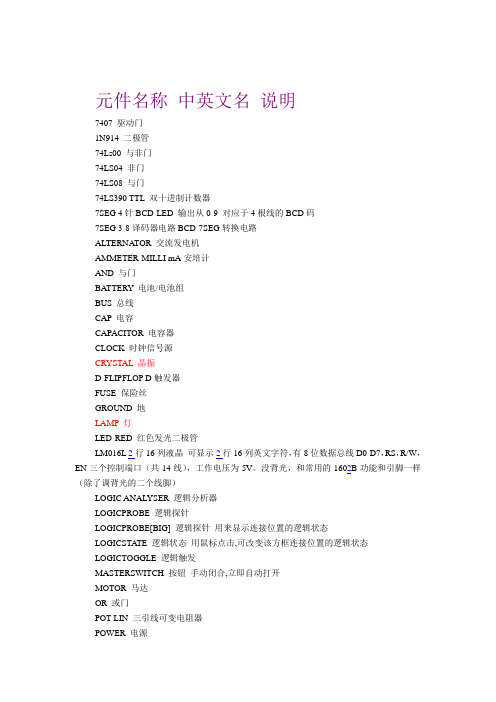
元件名称中英文名说明7407 驱动门1N914 二极管74Ls00 与非门74LS04 非门74LS08 与门74LS390 TTL 双十进制计数器7SEG 4针BCD-LED 输出从0-9 对应于4根线的BCD码7SEG 3-8译码器电路BCD-7SEG转换电路ALTERNATOR 交流发电机AMMETER-MILLI mA安培计AND 与门BA TTERY 电池/电池组BUS 总线CAP 电容CAPACITOR 电容器CLOCK 时钟信号源CRYSTAL 晶振D-FLIPFLOP D触发器FUSE 保险丝GROUND 地LAMP 灯LED-RED 红色发光二极管LM016L 2行16列液晶可显示2行16列英文字符,有8位数据总线D0-D7,RS,R/W,EN三个控制端口(共14线),工作电压为5V。
没背光,和常用的1602B功能和引脚一样(除了调背光的二个线脚)LOGIC ANAL YSER 逻辑分析器LOGICPROBE 逻辑探针LOGICPROBE[BIG] 逻辑探针用来显示连接位置的逻辑状态LOGICSTATE 逻辑状态用鼠标点击,可改变该方框连接位置的逻辑状态LOGICTOGGLE 逻辑触发MASTERSWITCH 按钮手动闭合,立即自动打开MOTOR 马达OR 或门POT-LIN 三引线可变电阻器POWER 电源RES 电阻PESPACK 排阻RESISTOR 电阻器SWITCH 按钮手动按一下一个状态SW-SPDT-mom 二选通一按钮触发开关BUTTONVOLTMETER 伏特计VOLTMETER-MILLI mV伏特计VTERM 串行口终端Electromechanical 电机Inductors 变压器Laplace Primitives 拉普拉斯变换Memory IcsMicroprocessor IcsMiscellaneous 各种器件AERIAL-天线;ATAHDD;ATMEGA64;BATTERY;CELL;CRYSTAL-晶振;FUSE;METER-仪表;Modelling Primitives 各种仿真器件是典型的基本元器模拟,不表示具体型号,只用于仿真,没有PCBOptoelectronics 各种发光器件发光二极管,LED,液晶等等PLDs & FPGAsResistors 各种电阻Simulator Primitives 常用的器件Speakers & SoundersSwitches & Relays 开关,继电器,键盘BUTTON 触发开关Switching Devices 晶阊管Transistors 晶体管(三极管,场效应管)TTL 74 seriesTTL 74ALS seriesTTL 74AS seriesTTL 74F seriesTTL 74HC seriesTTL 74HCT seriesTTL 74LS seriesTTL 74S seriesAnalog Ics 模拟电路集成芯片Capacitors 电容集合CMOS 4000 seriesConnectors 排座,排插Data Converters ADC,DACDebugging Tools 调试工具7SEG 数码管ECL 10000 Series 各种常用集成电路1.电阻固定电阻:RES半导体电阻:RESSEMT电位计;POT变电阻;RV AR可调电阻;res1可变电阻pot2.电容定值无极性电容;CAP定值有极性电容;CAP半导体电容:CAPSEMI可调电容:CAPV ARA700D3.电感:INDUCTOR4.二极管:DIODE.LIB发光二极管:LED5.三极管:NPN16.结型场效应管:JFET.lib7.MOS场效应管8.MES场效应管9.继电器:PELAY. LIB10.灯泡:LAMP11.运放:OPAMP12.数码管:7-SEG_DP (MISCELLANEOUS DEVICES.LIB)13.开关;sw_pb原理图常用库文件:Miscellaneous Devices.ddbDallas Microprocessor.ddbIntel Databooks.ddbProtel DOS Schematic Libraries.ddbPCB元件常用库:Advpcb.ddbGeneral IC.ddbMiscellaneous.ddb部分分立元件库元件名称及中英对照AND 与门ANTENNA 天线BA TTERY 直流电源BELL 铃,钟BVC 同轴电缆接插件BRIDEG 1 整流桥(二极管)BRIDEG 2整流桥(集成块)BUFFER 缓冲器BUZZER 蜂鸣器CAP 电容CAPACITOR 电容CAPACITOR POL 有极性电容CAPV AR 可调电容CIRCUIT BREAKER 熔断丝COAX 同轴电缆CON 插口CRYSTAL 晶体整荡器DB 并行插口DIODE 二极管DIODE SCHOTTKY 稳压二极管DIODE VARACTOR 变容二极管DPY_3-SEG 3段LEDDPY_7-SEG 7段LEDDPY_7-SEG_DP 7段LED(带小数点) ELECTRO电解电容FUSE 熔断器INDUCTOR 电感INDUCTOR IRON 带铁芯电感INDUCTOR3 可调电感JFET N N沟道场效应管JFET P P沟道场效应管LAMP 灯泡LAMP NEDN 起辉器LED 发光二极管METER 仪表MICROPHONE 麦克风MOSFET MOS管MOTOR AC 交流电机MOTOR SERVO 伺服电机NAND 与非门NOR 或非门NOT 非门NPN NPN三极管NPN-PHOTO 感光三极管OPAMP 运放OR 或门PHOTO 感光二极管PNP 三极管NPN DAR NPN三极管PNP DAR PNP三极管POT 滑线变阻器PELAY-DPDT 双刀双掷继电器RES1.2电阻RES3.4 可变电阻RESISTOR BRIDGE ? 桥式电阻RESPACK ? 电阻SCR 晶闸管PLUG ? 插头PLUG AC FEMALE 三相交流插头SOCKET ? 插座SOURCE CURRENT 电流源SOURCE VOLTAGE 电压源SPEAKER扬声器SW ? 开关SW-DPDY ? 双刀双掷开关SW-SPST ? 单刀单掷开关SW-PB 按钮THERMISTOR 电热调节器TRANS1 变压器TRANS2可调变压器TRIAC ? 三端双向可控硅TRIODE ? 三极真空管V ARISTOR 变阻器ZENER ? 齐纳二极管DPY_7-SEG_DP 数码管SW-PB 开关其他元件库Protel Dos Schematic 4000 Cmos .Lib (40.系列CMOS管集成块元件库)4013 D 触发器4027 JK 触发器Protel Dos Schematic Analog Digital.Lib(模拟数字式集成块元件库)AD系列DAC系列HD系列MC系列Protel Dos Schematic Comparator.Lib(比较放大器元件库)Protel Dos Shcematic Intel.Lib(INTEL公司生产的80系列CPU集成块元件库)Protel Dos Schematic Linear.lib(线性元件库)例555Protel Dos Schemattic Memory Devices.Lib(内存存储器元件库)Protel Dos Schematic SYnertek.Lib(SY系列集成块元件库)Protes Dos Schematic Motorlla.Lib(摩托罗拉公司生产的元件库)Protes Dos Schematic NEC.lib(NEC公司生产的集成块元件库)Protes Dos Schematic Operationel Amplifers.lib(运算放大器元件库)Protes Dos Schematic TTL.Lib(晶体管集成块元件库74系列)Protel Dos Schematic V oltage Regulator.lib(电压调整集成块元件库)Protes Dos Schematic Zilog.Lib(齐格格公司生产的Z80系列CPU集成块元件库)元件属性对话框中英文对照Lib ref 元件名称Footprint 器件封装Designator 元件称号Part 器件类别或标示值Schematic Tools 主工具栏Writing Tools 连线工具栏Drawing Tools 绘图工具栏稳压二极管ZENER DIODE肖特基二极管SCHOTTKY DIODE二极管DIODE变容二极管V ARIODE三极管TRANSISTOR电感INDUCTOR磁环EMIFIL电阻RESISTOR电容CAPACITY晶振CRYSTAL涤纶电容MYLAR CAP电解电容ELECT CAP瓷片电容CERAMIC CAP安规电容FILM CAPProtel 99 se的元件中英文PcbRe: [分享] protel99se 元件名系表--分立元件库中英文对照电阻AXIAL 无极性电容RAD 电解电容RB- 电位器VR 二极管DIODE 三极管TO 电源稳压块78和79系列TO-126H和TO-126V 场效应管和三极管一样整流桥D-44 D-37 D-46 单排多针插座CON SIP 双列直插元件DIP 晶振XTAL1电阻:RES1,RES2,RES3,RES4;封装属性为axial系列无极性电容:cap;封装属性为RAD-0.1到rad-0.4电解电容:electroi;封装属性为rb.2/.4到rb.5/1.0电位器:pot1,pot2;封装属性为vr-1到vr-5二极管:封装属性为diode-0.4(小功率)diode-0.7(大功率)三极管:常见的封装属性为to-18(普通三极管)to-22(大功率三极管)to-3(大功率达林顿管)电源稳压块有78和79系列;78系列如7805,7812,7820等79系列有7905,7912,7920等常见的封装属性有to126h和to126v整流桥:BRIDGE1,BRIDGE2: 封装属性为D系列(D-44,D-37,D-46)电阻:AXIAL0.3-AXIAL0.7其中0.4-0.7指电阻的长度,一般用AXIAL0.4 瓷片电容:RAD0.1-RAD0.3。
数字电路第4章(N2)
例2:
具有控制功能的 8位并-串并换器
1 2 3 4 5 6 7 8
§4-4-4 线性移位寄存器
移位寄存器可构成序列信号发生器,在通信及数字电 路故障检测中应用广泛。 若反馈函数为: S=C0⊕(C1Q1)⊕…⊕(CnQn)
§4-4-1 集成移位寄存器74194 集成移位寄存器74194
1. 常用集成移位寄存器
2. 74194的逻辑符号、逻辑功能
74194的标准逻辑符号
74194传统逻辑符号
行)输出、保持、清除等功能的4位双向移位寄存器。
74194功能:具有左移、右移、串(并行)输入、串(并
74194 功能表
四位双向移位寄存器74LS194构成八位双 向移动寄存器
D0 D1 D2 D3
16输出脉冲分配器 16输出脉冲分配器
§4-3-4 74192 双时钟模10加/减计数器 双时钟模10加
74192的标准逻辑符号
74192的传统逻辑符号
逻辑符号含义
74192的特性
74192的功能表
异步复位、异步预置的双时钟模10加 异步复位、异步预置的双时钟模10加/减计数器
§4-3 集成计数器其及应用
§4-3-1 §4-3-2 §4-3-3 §4-3-4 集成计数器 任意模计数器 计数器的扩展 集成计数器的应用举例
在数字电路中,能够记忆输入脉冲个数的 电路称为计数器。
计数器是一种非常典型、应用很广的时序电 路,除用于计数、分频外,还广泛用于数字测量 、运算和控制,从小型数字仪表,到大型数字电 子计算机,几乎无所不在,是任何现代数字系统 中不可缺少的组成部分。
由触发器构成同步计数器
Q2n 0 0 0 0 1 1 1 1
Q1n 0 0 1 1 0 0 1 1
N74F166D中文资料

元器件交易网DIP16:plastic dual in-line package; 16 leads (300 mil)SOT38-4SO16:plastic small outline package; 16 leads; body width 3.9 mm SOT109-1NOTES 1991 Feb 1411DefinitionsShort-form specification — The data in a short-form specification is extracted from a full data sheet with the same type number and title. For detailed information see the relevant data sheet or data handbook.Limiting values definition — Limiting values given are in accordance with the Absolute Maximum Rating System (IEC 134). Stress above one or more of the limiting values may cause permanent damage to the device. These are stress ratings only and operation of the device at these or at any other conditions above those given in the Characteristics sections of the specification is not implied. Exposure to limiting values for extended periods may affect device reliability.Application information — Applications that are described herein for any of these products are for illustrative purposes only. Philips Semiconductors make no representation or warranty that such applications will be suitable for the specified use without further testing or modification.DisclaimersLife support — These products are not designed for use in life support appliances, devices or systems where malfunction of these products can reasonably be expected to result in personal injury. Philips Semiconductors customers using or selling these products for use in such applications do so at their own risk and agree to fully indemnify Philips Semiconductors for any damages resulting from such application.Right to make changes — Philips Semiconductors reserves the right to make changes, without notice, in the products, including circuits, standard cells, and/or software, described or contained herein in order to improve design and/or performance. Philips Semiconductors assumes no responsibility or liability for the use of any of these products, conveys no license or title under any patent, copyright, or mask work right to these products, and makes no representations or warranties that these products are free from patent, copyright, or mask work right infringement, unless otherwise specified.Philips Semiconductors811 East Arques AvenueP.O. Box 3409Sunnyvale, California 94088–3409Telephone 800-234-7381© Copyright Philips Electronics North America Corporation 1998All rights reserved. Printed in U.S.A.print code Date of release: 10-98。
DM7406资料

© 2000 Fairchild Semiconductor Corporation DS006496December 1986Revised February 2000DM7406 Hex Inverting Buffers with High Voltage Open-Collector OutputsDM7406Hex Inverting Bufferswith High Voltage Open-Collector OutputsGeneral DescriptionThis device contains six independent buffers each of which performs the logic INVERT function. The open-collector outputs require external pull-up resistors for proper logical operation.Pull-Up Resistor EquationsWhere: N 1 (I OH ) = total maximum output high currentfor all outputs tied to pull-up resistorN 2 (I IH ) = total maximum input high current for all inputs tied to pull-up resistorN 3 (I IL ) = total maximum input low current for all inputs tied to pull-up resistorOrdering Code:Devices also available in T ape and Reel. Specify by appending the suffix letter “X” to the ordering code.Connection Diagram Function TableY = AH = HIGH Logic Level L = LOW Logic LevelOrder Number Package NumberPackage DescriptionDM7406M M14A 14-Lead Small Outline Integrated Circuit (SOIC), JEDEC MS-012, 0.150 Narrow DM7406NN14A14-Lead Plastic Dual-In-Line Package (PDIP), JEDEC MS-001, 0.300 WideInput Output A Y L H HL 2D M 7406Absolute Maximum Ratings (Note 1)Note 1: The “Absolute Maximum Ratings” are those values beyond which the safety of the device cannot be guaranteed. The device should not be operated at these limits. The parametric values defined in the Electrical Characteristics tables are not guaranteed at the absolute maximum ratings.The “Recommended Operating Conditions” table will define the conditions for actual device operation.Recommended Operating ConditionsElectrical Characteristicsover recommended operating free air temperature range (unless otherwise noted)Note 2: All typicals are at V CC = 5V, T A = 25°C.Switching Characteristicsat V CC = 5V and T A = 25°C Supply Voltage 7V Input Voltage 5.5V Output Voltage30VOperating Free Air Temperature Range 0°C to +70°C Storage Temperature Range−65°C to +150°CSymbol ParameterMin Nom Max Units V CC Supply Voltage4.7555.25V V IH HIGH Level Input Voltage 2V V IL LOW Level Input Voltage 0.8V V OH HIGH Level Output Voltage 30V I OL LOW Level Output Current 40mA T AFree Air Operating Temperature070°CSymbol ParameterConditionsMinTyp Max Units (Note 2)V I Input Clamp Voltage V CC = Min, I I = −12 mA −1.5V I CEX HIGH Level V CC = Min, V O = 30V 250µAOutput Current V IL = Max V OLLOW Level V CC = Min, I OL = Max0.7Output VoltageV IH = MinVI OL = 16 mA, V CC = Min 0.4I I Input Current @ Max Input Voltage V CC = Max, V I = 5.5V 1mA I IH HIGH Level Input Current V CC = Max, V I = 2.4V 40µA I IL LOW Level Input CurrentV CC = Max, V I = 0.4V −1.6mA I CCH Supply Current with Outputs HIGH V CC = Max 3048mA I CCLSupply Current with Outputs LOWV CC = Max2751mA Symbol ParameterConditionsMinMax Units t PLH Propagation Delay Time C L = 15 pF 15ns LOW-to-HIGH Level Output R L = 110Ωt PHLPropagation Delay Time 23nsHIGH-to-LOW Level OutputDM7406Physical Dimensions inches (millimeters) unless otherwise noted14-Lead Small Outline Integrated Circuit (SOIC), JEDEC MS-012, 0.150 NarrowPackage Number M14A4D M 7406 H e x I n v e r t i n g B u f f e r s w i t h H i g h V o l t a g e O p e n -C o l l e c t o r O u t p u t sPhysical Dimensions inches (millimeters) unless otherwise noted (Continued)14-Lead Plastic Dual-In-Line Package (PDIP), JEDEC MS-001, 0.300 WidePackage Number N14AFairchild does not assume any responsibility for use of any circuitry described, no circuit patent licenses are implied and Fairchild reserves the right at any time without notice to change said circuitry and specifications.LIFE SUPPORT POLICYFAIRCHILD’S PRODUCTS ARE NOT AUTHORIZED FOR USE AS CRITICAL COMPONENTS IN LIFE SUPPORT DEVICES OR SYSTEMS WITHOUT THE EXPRESS WRITTEN APPROVAL OF THE PRESIDENT OF FAIRCHILD SEMICONDUCTOR CORPORATION. As used herein:1.Life support devices or systems are devices or systems which, (a) are intended for surgical implant into the body, or (b) support or sustain life, and (c) whose failure to perform when properly used in accordance with instructions for use provided in the labeling, can be rea-sonably expected to result in a significant injury to the user. 2. A critical component in any component of a life support device or system whose failure to perform can be rea-sonably expected to cause the failure of the life support device or system, or to affect its safety or effectiveness.。
MC34063中文资料 引脚功能 应用电路

mc34063中文资料引脚功能应用电路简介:相关下载:mc34063中文资料pdf,MC34063A(MC33 063)集成电路芯片器件简介该器件本身包含了DC/DC变换器所需要的主要功能的单片控制电路且价格便宜。
它由...关键字:mc34063MC34063A(MC33063)集成电路芯片器件简介该器件本身包含了DC/DC变换器所需要的主要功能的单片控制电路且价格便宜。
它由具有温度自动补偿功能的基准电压发生器、比较器、占空比可控的振荡器,R—S触发器和大电流输出开关电路等组成。
该器件可用于升压变换器、降压变换器、反向器的控制核心,由它构成的DC/DC变换器仅用少量的外部元器件。
主要应用于以微处理器(MPU)或单片机(MCU)为基础的系统里。
MC34063集成电路主要特性:输入电压范围:2、5~40V输出电压可调范围:1.25~40V输出电流可达:1.5A工作频率:最高可达100kHz低静态电流短路电流限制可实现升压或降压电源变换器图2电压逆变器图3降压转换器图4NPN三极管扩流升压转换器图5NPN三极管扩流降压转换器图6升压转换器主要参数:项目条件参数单位Power SupplyVoltage电源电压VCC40VdcComparator Input VoltageRange比较器VIR0.3-+40Vdc输入电压范围Switch Collector Voltage 集电极电压开关VC(switch)40VdcSwitch Emitter Voltage(VP in1=40V)发射极电压开关VE(switch)40VdcSwitch Collector to Emitter Voltage开关电压集电极到发射极VCE(switch)40VdcDriver Collect or Voltage驱动集电极电压VC(driver)40VdcDriver Collector Current(N ote1)驱动集电极电流IC(driver)100mASwitch Current开关电流ISW 1.5A Operating Junction Temperature工作结温TJ+150℃Operating Ambient Temperature Range 操作环境温度范围TAMC3463A0-70℃MC3363AV40-125MC3340-8563AStorage Temperature RangTstg65-150℃e储存温度范围MC34063的工作原理MC34063组成的降压电路MC34063组成的降压电路原理如图7。
74数据大全
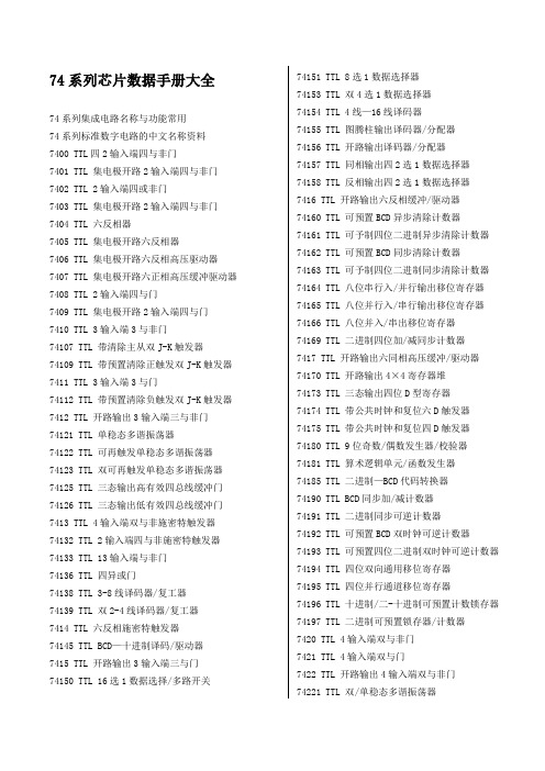
74系列芯片数据手册大全74系列集成电路名称与功能常用74系列标准数字电路的中文名称资料7400 TTL四2输入端四与非门7401 TTL 集电极开路2输入端四与非门7402 TTL 2输入端四或非门7403 TTL 集电极开路2输入端四与非门7404 TTL 六反相器7405 TTL 集电极开路六反相器7406 TTL 集电极开路六反相高压驱动器7407 TTL 集电极开路六正相高压缓冲驱动器7408 TTL 2输入端四与门7409 TTL 集电极开路2输入端四与门7410 TTL 3输入端3与非门74107 TTL 带清除主从双J-K触发器74109 TTL 带预置清除正触发双J-K触发器7411 TTL 3输入端3与门74112 TTL 带预置清除负触发双J-K触发器7412 TTL 开路输出3输入端三与非门74121 TTL 单稳态多谐振荡器74122 TTL 可再触发单稳态多谐振荡器74123 TTL 双可再触发单稳态多谐振荡器74125 TTL 三态输出高有效四总线缓冲门74126 TTL 三态输出低有效四总线缓冲门7413 TTL 4输入端双与非施密特触发器74132 TTL 2输入端四与非施密特触发器74133 TTL 13输入端与非门74136 TTL 四异或门74138 TTL 3-8线译码器/复工器74139 TTL 双2-4线译码器/复工器7414 TTL 六反相施密特触发器74145 TTL BCD—十进制译码/驱动器7415 TTL 开路输出3输入端三与门74150 TTL 16选1数据选择/多路开关74151 TTL 8选1数据选择器74153 TTL 双4选1数据选择器74154 TTL 4线—16线译码器74155 TTL 图腾柱输出译码器/分配器74156 TTL 开路输出译码器/分配器74157 TTL 同相输出四2选1数据选择器74158 TTL 反相输出四2选1数据选择器7416 TTL 开路输出六反相缓冲/驱动器74160 TTL 可预置BCD异步清除计数器74161 TTL 可予制四位二进制异步清除计数器74162 TTL 可预置BCD同步清除计数器74163 TTL 可予制四位二进制同步清除计数器74164 TTL 八位串行入/并行输出移位寄存器74165 TTL 八位并行入/串行输出移位寄存器74166 TTL 八位并入/串出移位寄存器74169 TTL 二进制四位加/减同步计数器7417 TTL 开路输出六同相高压缓冲/驱动器74170 TTL 开路输出4×4寄存器堆74173 TTL 三态输出四位D型寄存器74174 TTL 带公共时钟和复位六D触发器74175 TTL 带公共时钟和复位四D触发器74180 TTL 9位奇数/偶数发生器/校验器74181 TTL 算术逻辑单元/函数发生器74185 TTL 二进制—BCD代码转换器74190 TTL BCD同步加/减计数器74191 TTL 二进制同步可逆计数器74192 TTL 可预置BCD双时钟可逆计数器74193 TTL 可预置四位二进制双时钟可逆计数器74194 TTL 四位双向通用移位寄存器74195 TTL 四位并行通道移位寄存器74196 TTL 十进制/二-十进制可预置计数锁存器74197 TTL 二进制可预置锁存器/计数器7420 TTL 4输入端双与非门7421 TTL 4输入端双与门7422 TTL 开路输出4输入端双与非门74221 TTL 双/单稳态多谐振荡器74240 TTL 八反相三态缓冲器/线驱动器74241 TTL 八同相三态缓冲器/线驱动器74243 TTL 四同相三态总线收发器74244 TTL 八同相三态缓冲器/线驱动器74245 TTL 八同相三态总线收发器74247 TTL BCD—7段15V输出译码/驱动器74248 TTL BCD—7段译码/升压输出驱动器74249 TTL BCD—7段译码/开路输出驱动器7425 双4输入端或非门(有选通端74251 TTL 三态输出8选1数据选择器/复工器74253 TTL 三态输出双4选1数据选择器/复工器74256 TTL 双四位可寻址锁存器74257 TTL 三态原码四2选1数据选择器/复工器74258 TTL 三态反码四2选1数据选择器/复工器74259 TTL 八位可寻址锁存器/3-8线译码器7426 TTL 2输入端高压接口四与非门缓冲器74260 TTL 5输入端双或非门74266 TTL 2输入端四异或非门7427 TTL 3输入端三或非门74273 TTL 带公共时钟复位八D触发器74279 TTL 四图腾柱输出S-R锁存器7428 TTL 2输入端四或非门缓冲器74283 TTL 4位二进制全加器74290 TTL 二/五分频十进制计数器74293 TTL 二/八分频四位二进制计数器74295 TTL 四位双向通用移位寄存器74298 TTL 四2输入多路带存贮开关74299 TTL 三态输出八位通用移位寄存器7430 TTL 8输入端与非门7432 TTL 2输入端四或门74322 TTL 带符号扩展端八位移位寄存器74323 TTL 三态输出八位双向移位/存贮寄存器7433 TTL 开路输出2输入端四或非缓冲器74347 TTL BCD—7段译码器/驱动器74352 TTL 双4选1数据选择器/复工器74353 TTL 三态输出双4选1数据选择器/复工器74365 TTL 门使能输入三态输出六同相线驱动器74365 TTL 门使能输入三态输出六同相线驱动器74366 TTL 门使能输入三态输出六反相线驱动器74367 TTL 4/2线使能输入三态六同相线驱动器74368 TTL 4/2线使能输入三态六反相线驱动器7437 TTL 开路输出2输入端四与非缓冲器74373 TTL 三态同相八D锁存器74374 TTL 三态反相八D锁存器74375 TTL 4位双稳态锁存器74377 TTL 单边输出公共使能八D锁存器74378 TTL 单边输出公共使能六D锁存器74379 TTL 双边输出公共使能四D锁存器7438 TTL 开路输出2输入端四与非缓冲器74380 TTL 多功能八进制寄存器7439 TTL 开路输出2输入端四与非缓冲器74390 TTL 双十进制计数器74393 TTL 双四位二进制计数器7440 TTL 4输入端双与非缓冲器7442 TTL BCD—十进制代码转换器7443 4线-10线译码器(余3码输入)7444 4线-10线译码器(余3葛莱码输入) 74447 TTL BCD—7段译码器/驱动器7445 TTL BCD—十进制代码转换/驱动器74450 TTL 16:1多路转接复用器多工器74451 TTL 双8:1多路转接复用器多工器74453 TTL 四4:1多路转接复用器多工器7446 TTL BCD—7段低有效译码/驱动器74460 TTL 十位比较器74461 TTL 八进制计数器74465 TTL 三态同相2与使能端八总线缓冲器74466 TTL 三态反相2与使能八总线缓冲器74467 TTL 三态同相2使能端八总线缓冲器74468 TTL 三态反相2使能端八总线缓冲器74469 TTL 八位双向计数器7447 TTL BCD—7段高有效译码/驱动器7448 TTL BCD—7段译码器/内部上拉输出驱动7449 4线-7段译码器74490 TTL 双十进制计数器74491 TTL 十位计数器74498 TTL 八进制移位寄存器7450 TTL 2-3/2-2输入端双与或非门74502 TTL 八位逐次逼近寄存器74503 TTL 八位逐次逼近寄存器7451 TTL 2-3/2-2输入端双与或非门7452 4路2-3-2-2输入与或门7453 4路2-2-2-2输入与或非门74533 TTL 三态反相八D锁存器74534 TTL 三态反相八D锁存器7454 TTL 四路输入与或非门74540 TTL 八位三态反相输出总线缓冲器7455 TTL 4输入端二路输入与或非门74563 TTL 八位三态反相输出触发器74564 TTL 八位三态反相输出D触发器74573 TTL 八位三态输出触发器74574 TTL 八位三态输出D触发器7460 双4输入与扩展器7461 三3输入与扩展器7462 4路2-3-3-2输入与或扩展器7464 4路4-2-3-2输入与或非门74645 TTL 三态输出八同相总线传送接收器7465 4路4-2-3-2输入与或非门(OC)74670 TTL 三态输出4×4寄存器堆7470 与门输入J-K触发器√7471 与或门输入J-K触发器√7472 与门输入J-K触发器7473 TTL 带清除负触发双J-K触发器7474 TTL 带置位复位正触发双上升沿D触发器7476 TTL 带预置清除双J-K触发器7478 双D型触发器7483 TTL 四位二进制快速进位全加器7485 TTL 四位数字比较器7486 TTL 2输入端四异或门7487 4位二进制原码/反码7490 TTL 可二/五分频十进制计数器7493 TTL 可二/八分频二进制计数器7495 TTL 四位并行输入\输出移位寄存器7497 TTL 6位同步二进制乘法器74101 与或门输入J-K触发器74102 与门输入J-K触发器74107 双主-从J-K触发器74108 双主-从J-K触发器74109 双主-从J-K触发器74110 与门输入J-K触发器74111 双主-从J-K触发器74112 双下降沿J-K触发器113 双下降沿J-K触发器114 双下降沿J-K触发器116 双4位锁存器120 双脉冲同步驱动器121 单稳态触发器122 可重触发单稳态触发器123 可重触发双稳态触发器125 四总线缓冲器126 四总线缓冲器128 四2输入端或非线驱动器132 四2输入端与非门。
74系列芯片名称及解释
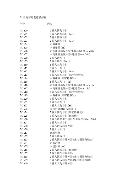
74系列芯片名称及解释型号内容---------------------------------------------------- 74ls00 2输入四与非门74ls01 2输入四与非门 (oc)74ls02 2输入四或非门74ls03 2输入四与非门 (oc)74ls04 六倒相器74ls05 六倒相器(oc)74ls06 六高压输出反相缓冲器/驱动器(oc,30v) 74ls07 六高压输出缓冲器/驱动器(oc,30v)74ls08 2输入四与门74ls09 2输入四与门(oc)74ls10 3输入三与非门74ls11 3输入三与门74ls12 3输入三与非门 (oc)74ls13 4输入双与非门 (斯密特触发)74ls14 六倒相器(斯密特触发)74ls15 3输入三与门 (oc)74ls16 六高压输出反相缓冲器/驱动器(oc,15v) 74ls17 六高压输出缓冲器/驱动器(oc,15v)74ls18 4输入双与非门 (斯密特触发)74ls19 六倒相器(斯密特触发)74ls20 4输入双与非门74ls21 4输入双与门74ls22 4输入双与非门(oc)74ls23 双可扩展的输入或非门74ls24 2输入四与非门(斯密特触发)74ls25 4输入双或非门(有选通)74ls26 2输入四高电平接口与非缓冲器(oc,15v) 74ls27 3输入三或非门74ls28 2输入四或非缓冲器74ls30 8输入与非门74ls31 延迟电路74ls32 2输入四或门74ls33 2输入四或非缓冲器(集电极开路输出)74ls34 六缓冲器74ls35 六缓冲器(oc)74ls36 2输入四或非门(有选通)74ls37 2输入四与非缓冲器74ls38 2输入四或非缓冲器(集电极开路输出)74ls39 2输入四或非缓冲器(集电极开路输出)74ls40 4输入双与非缓冲器74ls41 bcd-十进制计数器74ls42 4线-10线译码器(bcd输入)74ls43 4线-10线译码器(余3码输入)74ls44 4线-10线译码器(余3葛莱码输入)74ls45 bcd-十进制译码器/驱动器74ls46 bcd-七段译码器/驱动器74ls47 bcd-七段译码器/驱动器74ls48 bcd-七段译码器/驱动器74ls49 bcd-七段译码器/驱动器(oc)74ls50 双二路2-2输入与或非门(一门可扩展)74ls51 双二路2-2输入与或非门74ls51 二路3-3输入,二路2-2输入与或非门74ls52 四路2-3-2-2输入与或门(可扩展)74ls53 四路2-2-2-2输入与或非门(可扩展)74ls53 四路2-2-3-2输入与或非门(可扩展)74ls54 四路2-2-2-2输入与或非门74ls54 四路2-3-3-2输入与或非门74ls54 四路2-2-3-2输入与或非门74ls55 二路4-4输入与或非门(可扩展)74ls60 双四输入与扩展74ls61 三3输入与扩展74ls62 四路2-3-3-2输入与或扩展器74ls63 六电流读出接口门74ls64 四路4-2-3-2输入与或非门74ls65 四路4-2-3-2输入与或非门(oc)74ls70 与门输入上升沿jk触发器74ls71 与输入r-s主从触发器74ls72 与门输入主从jk触发器74ls73 双j-k触发器(带清除端)74ls74 正沿触发双d型触发器(带预置端和清除端)74ls75 4位双稳锁存器74ls76 双j-k触发器(带预置端和清除端)74ls77 4位双稳态锁存器74ls78 双j-k触发器(带预置端,公共清除端和公共时钟端) 74ls80 门控全加器74ls81 16位随机存取存储器74ls82 2位二进制全加器(快速进位)74ls83 4位二进制全加器(快速进位)74ls84 16位随机存取存储器74ls85 4位数字比较器74ls86 2输入四异或门74ls87 四位二进制原码/反码/oi单元74ls89 64位读/写存储器74ls90 十进制计数器74ls91 八位移位寄存器74ls92 12分频计数器(2分频和6分频)74ls93 4位二进制计数器74ls94 4位移位寄存器(异步)74ls95 4位移位寄存器(并行io)74ls96 5位移位寄存器74ls97 六位同步二进制比率乘法器74ls100 八位双稳锁存器74ls103 负沿触发双j-k主从触发器(带清除端)74ls106 负沿触发双j-k主从触发器(带预置,清除,时钟) 74ls107 双j-k主从触发器(带清除端)74ls108 双j-k主从触发器(带预置,清除,时钟)74ls109 双j-k触发器(带置位,清除,正触发)74ls110 与门输入j-k主从触发器(带锁定)74ls111 双j-k主从触发器(带数据锁定)74ls112 负沿触发双j-k触发器(带预置端和清除端)74ls113 负沿触发双j-k触发器(带预置端)74ls114 双j-k触发器(带预置端,共清除端和时钟端)74ls116 双四位锁存器74ls120 双脉冲同步器/驱动器74ls121 单稳态触发器(施密特触发)74ls122 可再触发单稳态多谐振荡器(带清除端)74ls123 可再触发双单稳多谐振荡器74ls125 四总线缓冲门(三态输出)74ls126 四总线缓冲门(三态输出)74ls128 2输入四或非线驱动器74ls131 3-8译码器74ls132 2输入四与非门(斯密特触发)74ls133 13输入端与非门74ls134 12输入端与门(三态输出)74ls135 四异或/异或非门74ls136 2输入四异或门(oc)74ls137 八选1锁存译码器/多路转换器74ls138 3-8线译码器/多路转换器74ls139 双2-4线译码器/多路转换器74ls140 双4输入与非线驱动器74ls141 bcd-十进制译码器/驱动器74ls142 计数器/锁存器/译码器/驱动器74ls145 4-10译码器/驱动器74ls147 10线-4线优先编码器74ls148 8线-3线八进制优先编码器74ls150 16选1数据选择器(反补输出)74ls151 8选1数据选择器(互补输出)74ls152 8选1数据选择器多路开关74ls153 双4选1数据选择器/多路选择器74ls154 4线-16线译码器74ls155 双2-4译码器/分配器(图腾柱输出)74ls156 双2-4译码器/分配器(集电极开路输出) 74ls157 四2选1数据选择器/多路选择器74ls158 四2选1数据选择器(反相输出)74ls160 可预置bcd计数器(异步清除)74ls161 可预置四位二进制计数器(并清除异步) 74ls162 可预置bcd计数器(异步清除)74ls163 可预置四位二进制计数器(并清除异步) 74ls164 8位并行输出串行移位寄存器74ls165 并行输入8位移位寄存器(补码输出)74ls166 8位移位寄存器74ls167 同步十进制比率乘法器74ls168 4位加/减同步计数器(十进制)74ls169 同步二进制可逆计数器74ls170 4*4寄存器堆74ls171 四d触发器(带清除端)74ls172 16位寄存器堆74ls173 4位d型寄存器(带清除端)74ls174 六d触发器74ls175 四d触发器74ls176 十进制可预置计数器74ls177 2-8-16进制可预置计数器74ls178 四位通用移位寄存器74ls179 四位通用移位寄存器74ls180 九位奇偶产生/校验器74ls181 算术逻辑单元/功能发生器74ls182 先行进位发生器74ls183 双保留进位全加器74ls184 bcd-二进制转换器74ls185 二进制-bcd转换器74ls190 同步可逆计数器(bcd,二进制)74ls191 同步可逆计数器(bcd,二进制)74ls192 同步可逆计数器(bcd,二进制)74ls193 同步可逆计数器(bcd,二进制)74ls194 四位双向通用移位寄存器74ls195 四位通用移位寄存器74ls196 可预置计数器/锁存器74ls197 可预置计数器/锁存器(二进制)74ls198 八位双向移位寄存器74ls199 八位移位寄存器74ls210 2-5-10进制计数器74ls213 2-n-10可变进制计数器74ls221 双单稳触发器74ls230 八3态总线驱动器74ls231 八3态总线反向驱动器74ls240 八缓冲器/线驱动器/线接收器(反码三态输出) 74ls241 八缓冲器/线驱动器/线接收器(原码三态输出) 74ls242 八缓冲器/线驱动器/线接收器74ls243 4同相三态总线收发器74ls244 八缓冲器/线驱动器/线接收器74ls245 八双向总线收发器74ls246 4线-七段译码/驱动器(30v)74ls247 4线-七段译码/驱动器(15v)74ls248 4线-七段译码/驱动器74ls249 4线-七段译码/驱动器74ls251 8选1数据选择器(三态输出)74ls253 双四选1数据选择器(三态输出)74ls256 双四位可寻址锁存器74ls257 四2选1数据选择器(三态输出)74ls258 四2选1数据选择器(反码三态输出)74ls259 8为可寻址锁存器74ls260 双5输入或非门74ls261 4*2并行二进制乘法器74ls265 四互补输出元件74ls266 2输入四异或非门(oc)74ls270 2048位rom (512位四字节,oc)74ls271 2048位rom (256位八字节,oc)74ls273 八d触发器74ls274 4*4并行二进制乘法器74ls275 七位片式华莱士树乘法器74ls276 四jk触发器74ls278 四位可级联优先寄存器74ls279 四s-r锁存器74ls280 9位奇数/偶数奇偶发生器/较验器74ls28174ls283 4位二进制全加器74ls290 十进制计数器74ls291 32位可编程模74ls293 4位二进制计数器74ls294 16位可编程模74ls295 四位双向通用移位寄存器74ls298 四-2输入多路转换器(带选通)74ls299 八位通用移位寄存器(三态输出)74ls348 8-3线优先编码器(三态输出)74ls352 双四选1数据选择器/多路转换器74ls353 双4-1线数据选择器(三态输出)74ls354 8输入端多路转换器/数据选择器/寄存器,三态补码输出74ls355 8输入端多路转换器/数据选择器/寄存器,三态补码输出74ls356 8输入端多路转换器/数据选择器/寄存器,三态补码输出74ls357 8输入端多路转换器/数据选择器/寄存器,三态补码输出74ls365 6总线驱动器74ls366 六反向三态缓冲器/线驱动器74ls367 六同向三态缓冲器/线驱动器74ls368 六反向三态缓冲器/线驱动器74ls373 八d锁存器74ls374 八d触发器(三态同相)74ls375 4位双稳态锁存器74ls377 带使能的八d触发器74ls378 六d触发器74ls379 四d触发器74ls381 算术逻辑单元/函数发生器74ls382 算术逻辑单元/函数发生器74ls384 8位*1位补码乘法器74ls385 四串行加法器/乘法器74ls386 2输入四异或门74ls390 双十进制计数器74ls391 双四位二进制计数器74ls395 4位通用移位寄存器74ls396 八位存储寄存器74ls398 四2输入端多路开关(双路输出)74ls399 四-2输入多路转换器(带选通)74ls422 单稳态触发器74ls423 双单稳态触发器74ls440 四3方向总线收发器,集电极开路74ls441 四3方向总线收发器,集电极开路74ls442 四3方向总线收发器,三态输出74ls443 四3方向总线收发器,三态输出74ls444 四3方向总线收发器,三态输出74ls445 bcd-十进制译码器/驱动器,三态输出74ls446 有方向控制的双总线收发器74ls448 四3方向总线收发器,三态输出74ls449 有方向控制的双总线收发器74ls465 八三态线缓冲器74ls466 八三态线反向缓冲器74ls467 八三态线缓冲器74ls468 八三态线反向缓冲器74ls490 双十进制计数器74ls540 八位三态总线缓冲器(反向)74ls541 八位三态总线缓冲器74ls589 有输入锁存的并入串出移位寄存器74ls590 带输出寄存器的8位二进制计数器74ls591 带输出寄存器的8位二进制计数器74ls592 带输出寄存器的8位二进制计数器74ls593 带输出寄存器的8位二进制计数器74ls594 带输出锁存的8位串入并出移位寄存器74ls595 8位输出锁存移位寄存器74ls596 带输出锁存的8位串入并出移位寄存器74ls597 8位输出锁存移位寄存器74ls598 带输入锁存的并入串出移位寄存器74ls599 带输出锁存的8位串入并出移位寄存器74ls604 双8位锁存器74ls605 双8位锁存器74ls606 双8位锁存器74ls607 双8位锁存器74ls620 8位三态总线发送接收器(反相)74ls621 8位总线收发器74ls622 8位总线收发器74ls623 8位总线收发器74ls640 反相总线收发器(三态输出)74ls641 同相8总线收发器,集电极开路74ls642 同相8总线收发器,集电极开路74ls643 8位三态总线发送接收器74ls644 真值反相8总线收发器,集电极开路74ls645 三态同相8总线收发器74ls646 八位总线收发器,寄存器74ls647 八位总线收发器,寄存器74ls648 八位总线收发器,寄存器74ls649 八位总线收发器,寄存器74ls651 三态反相8总线收发器74ls652 三态反相8总线收发器74ls653 反相8总线收发器,集电极开路74ls654 同相8总线收发器,集电极开路74ls668 4位同步加/减十进制计数器74ls669 带先行进位的4位同步二进制可逆计数器74ls670 4*4寄存器堆(三态)74ls671 带输出寄存的四位并入并出移位寄存器74ls672 带输出寄存的四位并入并出移位寄存器74ls673 16位并行输出存储器,16位串入串出移位寄存器74ls674 16位并行输入串行输出移位寄存器74ls681 4位并行二进制累加器74ls682 8位数值比较器(图腾柱输出)74ls683 8位数值比较器(集电极开路)74ls684 8位数值比较器(图腾柱输出)74ls685 8位数值比较器(集电极开路)74ls686 8位数值比较器(图腾柱输出)74ls687 8位数值比较器(集电极开路)74ls688 8位数字比较器(oc输出)74ls689 8位数字比较器74ls690 同步十进制计数器/寄存器(带数选,三态输出,直接清除)74ls691 计数器/寄存器(带多转换,三态输出)74ls692 同步十进制计数器(带预置输入,同步清除)74ls693 计数器/寄存器(带多转换,三态输出)74ls696 同步加/减十进制计数器/寄存器(带数选,三态输出,直接清除)74ls697 计数器/寄存器(带多转换,三态输出)74ls698 计数器/寄存器(带多转换,三态输出)74ls699 计数器/寄存器(带多转换,三态输出)74ls716 可编程模n十进制计数器74ls718 可编程模n十进制计数器/bbs/read.php?fid=10&tid=14&fpage=174HC/LS/HCT/F系列芯片的区别1、 LS是低功耗肖特基,HC是高速COMS。
SN74193N中文资料

Copyright © 1988, Texas Instruments Incorporated PRODUCTION DATA information is current as of publication date.Products conform to specifications per the terms of Texas Instrumentsstandard warranty. Production processing does not necessarily includetesting of all parameters.PACKAGING INFORMATIONOrderable Device Status(1)PackageType PackageDrawingPins PackageQtyEco Plan(2)Lead/Ball Finish MSL Peak Temp(3)5962-9558401QEA ACTIVE CDIP J161TBD Call TI Level-NC-NC-NC 5962-9558401QFA ACTIVE CFP W161TBD Call TI Level-NC-NC-NC 5962-9558401QFA ACTIVE CFP W161TBD Call TI Level-NC-NC-NC 76006012A ACTIVE LCCC FK201TBD Call TI Level-NC-NC-NC 76006012A ACTIVE LCCC FK201TBD Call TI Level-NC-NC-NC 7600601EA ACTIVE CDIP J161TBD Call TI Level-NC-NC-NC 7600601EA ACTIVE CDIP J161TBD Call TI Level-NC-NC-NC 7600601FA ACTIVE CFP W161TBD Call TI Level-NC-NC-NC 7600601FA ACTIVE CFP W161TBD Call TI Level-NC-NC-NCJM38510/01309BEA OBSOLETE CDIP J16TBD Call TI Call TIJM38510/01309BEA OBSOLETE CDIP J16TBD Call TI Call TIJM38510/31508B2A ACTIVE LCCC FK201TBD Call TI Level-NC-NC-NCJM38510/31508B2A ACTIVE LCCC FK201TBD Call TI Level-NC-NC-NCJM38510/31508BEA ACTIVE CDIP J161TBD Call TI Level-NC-NC-NCJM38510/31508BEA ACTIVE CDIP J161TBD Call TI Level-NC-NC-NCJM38510/31508BFA ACTIVE CFP W161TBD Call TI Level-NC-NC-NCJM38510/31508BFA ACTIVE CFP W161TBD Call TI Level-NC-NC-NCJM38510/31508SEA ACTIVE CDIP J161TBD Call TI Level-NC-NC-NCJM38510/31508SEA ACTIVE CDIP J161TBD Call TI Level-NC-NC-NCJM38510/31508SFA ACTIVE CFP W161TBD Call TI Level-NC-NC-NCJM38510/31508SFA ACTIVE CFP W161TBD Call TI Level-NC-NC-NC SN54192J ACTIVE CDIP J161TBD Call TI Level-NC-NC-NC SN54192J ACTIVE CDIP J161TBD Call TI Level-NC-NC-NC SN54193J OBSOLETE CDIP J16TBD Call TI Call TISN54193J OBSOLETE CDIP J16TBD Call TI Call TISN54LS193J ACTIVE CDIP J161TBD Call TI Level-NC-NC-NC SN54LS193J ACTIVE CDIP J161TBD Call TI Level-NC-NC-NC SN74192N OBSOLETE PDIP N16TBD Call TI Call TISN74192N OBSOLETE PDIP N16TBD Call TI Call TISN74193N OBSOLETE PDIP N16TBD Call TI Call TISN74193N OBSOLETE PDIP N16TBD Call TI Call TISN74193N3OBSOLETE PDIP N16TBD Call TI Call TISN74193N3OBSOLETE PDIP N16TBD Call TI Call TISN74LS192D OBSOLETE SOIC D16TBD Call TI Call TISN74LS192D OBSOLETE SOIC D16TBD Call TI Call TISN74LS192N OBSOLETE PDIP N16TBD Call TI Call TISN74LS192N OBSOLETE PDIP N16TBD Call TI Call TISN74LS193D ACTIVE SOIC D1640Green(RoHS&no Sb/Br)CU NIPDAU Level-2-260C-1YEARSN74LS193D ACTIVE SOIC D1640Green(RoHS&no Sb/Br)CU NIPDAU Level-2-260C-1YEARSN74LS193DE4ACTIVE SOIC D1640Green(RoHS&no Sb/Br)CU NIPDAU Level-2-260C-1YEAROrderable Device Status(1)PackageType PackageDrawingPins PackageQtyEco Plan(2)Lead/Ball Finish MSL Peak Temp(3)SN74LS193DE4ACTIVE SOIC D1640Green(RoHS&no Sb/Br)CU NIPDAU Level-2-260C-1YEARSN74LS193DR ACTIVE SOIC D162500Green(RoHS&no Sb/Br)CU NIPDAU Level-2-260C-1YEARSN74LS193DR ACTIVE SOIC D162500Green(RoHS&no Sb/Br)CU NIPDAU Level-2-260C-1YEARSN74LS193DRE4ACTIVE SOIC D162500Green(RoHS&no Sb/Br)CU NIPDAU Level-2-260C-1YEARSN74LS193DRE4ACTIVE SOIC D162500Green(RoHS&no Sb/Br)CU NIPDAU Level-2-260C-1YEAR SN74LS193J OBSOLETE CDIP J16TBD Call TI Call TISN74LS193J OBSOLETE CDIP J16TBD Call TI Call TISN74LS193N ACTIVE PDIP N1625Pb-Free(RoHS)CU NIPDAU Level-NC-NC-NCSN74LS193N ACTIVE PDIP N1625Pb-Free(RoHS)CU NIPDAU Level-NC-NC-NC SN74LS193N3OBSOLETE PDIP N16TBD Call TI Call TISN74LS193N3OBSOLETE PDIP N16TBD Call TI Call TISN74LS193NE4ACTIVE PDIP N1625Pb-Free(RoHS)CU NIPDAU Level-NC-NC-NCSN74LS193NE4ACTIVE PDIP N1625Pb-Free(RoHS)CU NIPDAU Level-NC-NC-NCSN74LS193NSR ACTIVE SO NS162000Green(RoHS&no Sb/Br)CU NIPDAU Level-1-260C-UNLIMSN74LS193NSR ACTIVE SO NS162000Green(RoHS&no Sb/Br)CU NIPDAU Level-1-260C-UNLIMSN74LS193NSRE4ACTIVE SO NS162000Green(RoHS&no Sb/Br)CU NIPDAU Level-1-260C-UNLIMSN74LS193NSRE4ACTIVE SO NS162000Green(RoHS&no Sb/Br)CU NIPDAU Level-1-260C-UNLIM SNJ54192J ACTIVE CDIP J161TBD Call TI Level-NC-NC-NCSNJ54192J ACTIVE CDIP J161TBD Call TI Level-NC-NC-NCSNJ54192W ACTIVE CFP W161TBD Call TI Level-NC-NC-NCSNJ54192W ACTIVE CFP W161TBD Call TI Level-NC-NC-NCSNJ54193J OBSOLETE CDIP J16TBD Call TI Call TISNJ54193J OBSOLETE CDIP J16TBD Call TI Call TISNJ54193W OBSOLETE CFP W16TBD Call TI Call TISNJ54193W OBSOLETE CFP W16TBD Call TI Call TISNJ54LS193FK ACTIVE LCCC FK201TBD Call TI Level-NC-NC-NC SNJ54LS193FK ACTIVE LCCC FK201TBD Call TI Level-NC-NC-NC SNJ54LS193J ACTIVE CDIP J161TBD Call TI Level-NC-NC-NC SNJ54LS193J ACTIVE CDIP J161TBD Call TI Level-NC-NC-NC SNJ54LS193W ACTIVE CFP W161TBD Call TI Level-NC-NC-NC SNJ54LS193W ACTIVE CFP W161TBD Call TI Level-NC-NC-NC (1)The marketing status values are defined as follows:ACTIVE:Product device recommended for new designs.LIFEBUY:TI has announced that the device will be discontinued,and a lifetime-buy period is in effect.NRND:Not recommended for new designs.Device is in production to support existing customers,but TI does not recommend using this part ina new design.PREVIEW:Device has been announced but is not in production.Samples may or may not be available.OBSOLETE:TI has discontinued the production of the device.(2)Eco Plan-The planned eco-friendly classification:Pb-Free(RoHS)or Green(RoHS&no Sb/Br)-please check /productcontent for the latest availability information and additional product content details.TBD:The Pb-Free/Green conversion plan has not been defined.Pb-Free(RoHS):TI's terms"Lead-Free"or"Pb-Free"mean semiconductor products that are compatible with the current RoHS requirements for all6substances,including the requirement that lead not exceed0.1%by weight in homogeneous materials.Where designed to be soldered at high temperatures,TI Pb-Free products are suitable for use in specified lead-free processes.Green(RoHS&no Sb/Br):TI defines"Green"to mean Pb-Free(RoHS compatible),and free of Bromine(Br)and Antimony(Sb)based flame retardants(Br or Sb do not exceed0.1%by weight in homogeneous material)(3)MSL,Peak Temp.--The Moisture Sensitivity Level rating according to the JEDEC industry standard classifications,and peak solder temperature.Important Information and Disclaimer:The information provided on this page represents TI's knowledge and belief as of the date that it is provided.TI bases its knowledge and belief on information provided by third parties,and makes no representation or warranty as to the accuracy of such information.Efforts are underway to better integrate information from third parties.TI has taken and continues to take reasonable steps to provide representative and accurate information but may not have conducted destructive testing or chemical analysis on incoming materials and chemicals.TI and TI suppliers consider certain information to be proprietary,and thus CAS numbers and other limited information may not be available for release.In no event shall TI's liability arising out of such information exceed the total purchase price of the TI part(s)at issue in this document sold by TI to Customer on an annual basis.IMPORTANT NOTICETexas Instruments Incorporated and its subsidiaries (TI) reserve the right to make corrections, modifications, enhancements, improvements, and other changes to its products and services at any time and to discontinue any product or service without notice. Customers should obtain the latest relevant information before placing orders and should verify that such information is current and complete. All products are sold subject to TI’s terms and conditions of sale supplied at the time of order acknowledgment.TI warrants performance of its hardware products to the specifications applicable at the time of sale in accordance with TI’s standard warranty. T esting and other quality control techniques are used to the extent TI deems necessary to support this warranty. Except where mandated by government requirements, testing of all parameters of each product is not necessarily performed.TI assumes no liability for applications assistance or customer product design. Customers are responsible for their products and applications using TI components. T o minimize the risks associated with customer products and applications, customers should provide adequate design and operating safeguards.TI does not warrant or represent that any license, either express or implied, is granted under any TI patent right, copyright, mask work right, or other TI intellectual property right relating to any combination, machine, or process in which TI products or services are used. Information published by TI regarding third-party products or services does not constitute a license from TI to use such products or services or a warranty or endorsement thereof. Use of such information may require a license from a third party under the patents or other intellectual property of the third party, or a license from TI under the patents or other intellectual property of TI.Reproduction of information in TI data books or data sheets is permissible only if reproduction is without alteration and is accompanied by all associated warranties, conditions, limitations, and notices. Reproduction of this information with alteration is an unfair and deceptive business practice. TI is not responsible or liable for such altered documentation.Resale of TI products or services with statements different from or beyond the parameters stated by TI for that product or service voids all express and any implied warranties for the associated TI product or service and is an unfair and deceptive business practice. TI is not responsible or liable for any such statements. Following are URLs where you can obtain information on other Texas Instruments products and application solutions:Products ApplicationsAmplifiers Audio /audioData Converters Automotive /automotiveDSP Broadband /broadbandInterface Digital Control /digitalcontrolLogic Military /militaryPower Mgmt Optical Networking /opticalnetwork Microcontrollers Security /securityTelephony /telephonyVideo & Imaging /videoWireless /wirelessMailing Address:Texas InstrumentsPost Office Box 655303 Dallas, Texas 75265Copyright 2005, Texas Instruments Incorporated。
7433中文资料

© 2000 Fairchild Semiconductor Corporation DS006361June 1986Revised March 2000DM74LS32 Quad 2-Input OR GateDM74LS32Quad 2-Input OR GateGeneral DescriptionThis device contains four independent gates each of which performs the logic OR function.Ordering Code:Devices also available in T ape and Reel. Specify by appending the suffix letter “X” to the ordering code.Connection Diagram Function TableY = A + B H = HIGH Logic Level L = LOW Logic LevelOrder Number Package NumberPackage DescriptionDM74LS32M M14A 14-Lead Small Outline Integrated Circuit (SOIC), JEDEC MS-120, 0.150 Narrow DM74LS32SJ M14D 14-Lead Small Outline Package (SOP), EIAJ TYPE II, 5.3mm Wide DM74LS32NN14A14-Lead Plastic Dual-In-Line Package (PDIP), JEDEC MS-001, 0.300 WideInputs OutputA B Y L L L L H H H L H HHH 2D M 74L S 32Absolute Maximum Ratings (Note 1)Note 1: The “Absolute Maximum Ratings” are those values beyond which the safety of the device cannot be guaranteed. The device should not be operated at these limits. The parametric values defined in the Electrical Characteristics tables are not guaranteed at the absolute maximum ratings.The “Recommended Operating Conditions” table will define the conditions for actual device operation.Recommended Operating ConditionsElectrical Characteristicsover recommended operating free air temperature range (unless otherwise noted)Note 2: All typicals are at V CC = 5V, T A = 25°C.Note 3: Not more than one output should be shorted at a time, and the duration should not exceed one second.Switching Characteristicsat V CC = 5V and T A = 25°CSupply Voltage 7V Input Voltage7VOperating Free Air Temperature Range 0°C to +70°C Storage Temperature Range−65°C to +150°CSymbol ParameterMin Nom Max Units V CC Supply Voltage4.7555.25V V IH HIGH Level Input Voltage 2V V IL LOW Level Input Voltage 0.8V I OH HIGH Level Output Current −0.4mA I OL LOW Level Output Current 8mA T AFree Air Operating Temperature70°CSymbol ParameterConditionsMinTyp Max Units (Note 2)V I Input Clamp Voltage V CC = Min, I I = −18 mA −1.5V V OH HIGH Level V CC = Min, I OH = Max 2.73.4VOutput Voltage V IH = Min V OLLOW Level V CC = Min, I OL = Max0.350.5Output VoltageV IL = MaxVI OL = 4 mA, V CC = Min 0.250.4I I Input Current @ Max Input Voltage V CC = Max, V I = 7V 0.1mA I IH HIGH Level Input Current V CC = Max, V I = 2.7V 20µA I IL LOW Level Input Current V CC = Max, V I = 0.4V −0.36mA I OS Short Circuit Output Current V CC = Max (Note 3)−20−100mA I CCH Supply Current with Outputs HIGH V CC = Max 3.1 6.2mA I CCLSupply Current with Outputs LOWV CC = Max4.99.8mAR L = 2 k ΩSymbol ParameterC L = 15 pFC L = 50 pFUnitsMinMax Min Max t PLH Propagation Delay Time 311415ns LOW-to-HIGH Level Output t PHLPropagation Delay Time 311415ns HIGH-to-LOW Level OutputDM74LS32Physical Dimensions inches (millimeters) unless otherwise noted14-Lead Small Outline Integrated Circuit (SOIC), JEDEC MS-120, 0.150 NarrowPackage Number M14A 4D M 74L S 32Physical Dimensionsinches (millimeters) unless otherwise noted (Continued)14-Lead Small Outline Package (SOP), EIAJ TYPE II, 5.3mm WidePackage Number M14D5DM74LS32 Quad 2-Input OR GatePhysical Dimensions inches (millimeters) unless otherwise noted (Continued)14-Lead Plastic Dual-In-Line Package (PDIP), JEDEC MS-001, 0.300 WidePackage Number N14AFairchild does not assume any responsibility for use of any circuitry described, no circuit patent licenses are implied and Fairchild reserves the right at any time without notice to change said circuitry and specifications.LIFE SUPPORT POLICYFAIRCHILD’S PRODUCTS ARE NOT AUTHORIZED FOR USE AS CRITICAL COMPONENTS IN LIFE SUPPORT DEVICES OR SYSTEMS WITHOUT THE EXPRESS WRITTEN APPROVAL OF THE PRESIDENT OF FAIRCHILD SEMICONDUCTOR CORPORATION. As used herein:1.Life support devices or systems are devices or systems which, (a) are intended for surgical implant into the body, or (b) support or sustain life, and (c) whose failure to perform when properly used in accordance with instructions for use provided in the labeling, can be rea-sonably expected to result in a significant injury to the user.2. A critical component in any component of a life support device or system whose failure to perform can be rea-sonably expected to cause the failure of the life support device or system, or to affect its safety or effectiveness.。
DM74163N资料

TL F 6551DM54161 DM74161 DM74163 Synchronous 4-Bit CountersOctober1992 DM54161 DM74161 DM74163Synchronous4-Bit CountersGeneral DescriptionThese synchronous presettable counters feature an inter-nal carry look-ahead for application in high-speed countingdesigns The161and163are4-bit binary counters Thecarry output is decoded by means of a NOR gate thus pre-venting spikes during the normal counting mode of opera-tion Synchronous operation is provided by having all flip-flops clocked simultaneously so that the outputs change co-incident with each other when so instructed by the count-enable inputs and internal gating This mode of operationeliminates the output counting spikes which are normallyassociated with asynchronous(ripple clock)counters Abuffered clock input triggers the four flip-flops on the rising(positive-going)edge of the clock input waveformThese counters are fully programmable that is the outputsmay be preset to either level As presetting is synchronoussetting up a low level at the load input disables the counterand causes the outputs to agree with the setup data afterthe next clock pulse regardless of the levels of the enableinput The clear function for the161is asynchronous and alow level at the clear input sets all four of the flip-flop out-puts low regardless of the levels of clock load or enableinputs The clear function for the163is synchronous and alow level at the clear input sets all four of the flip-flop out-puts low after the next clock pulse regardless of the levelsof the enable inputs This synchronous clear allows thecount length to be modified easily as decoding the maxi-mum count desired can be accomplished with oneexternal NAND gate The gate output is connected to theclear input to synchronously clear the counter to all low out-puts Low-to-high transitions at the clear input of the163arealso permissible regardless of the logic levels on the clockenable or load inputsThe carry look-ahead circuitry provides for cascading coun-ters for n-bit synchronous applications without additionalgating Instrumental in accomplishing this function are twocount-enable inputs and a ripple carry output Both count-enable inputs(P and T)must be high to count and input T isfed forward to enable the ripple carry output The ripple car-ry output thus enabled will produce a high-level output pulsewith a duration approximately equal to the high-level portionof the Q A output This high-level overflow ripple carry pulsecan be used to enable successive cascaded stages High-to-low-level transitions at the enable P or T inputs of the161through163may occur regardless of the logic level on theclockFeaturesY Synchronously programmableY Internal look-ahead for fast countingY Carry output for n-bit cascadingY Synchronous countingY Load control lineY Diode-clamped inputsConnection DiagramDual-In-Line PackageTL F 6551–1Order Number DM54161J DM54161WDM74161N or DM74163NSee NS Package Number J16A N16E or W16AC1995National Semiconductor Corporation RRD-B30M105 Printed in U S AAbsolute Maximum Ratings(Note)If Military Aerospace specified devices are required please contact the National Semiconductor Sales Office Distributors for availability and specifications Supply Voltage7V Input Voltage5 5V Operating Free Air Temperature RangeDM54b55 C to a125 C DM740 C to a70 C Storage Temperature Range b65 C to a150 C Note The‘‘Absolute Maximum Ratings’’are those values beyond which the safety of the device cannot be guaran-teed The device should not be operated at these limits The parametric values defined in the‘‘Electrical Characteristics’’table are not guaranteed at the absolute maximum ratings The‘‘Recommended Operating Conditions’’table will define the conditions for actual device operationRecommended Operating ConditionsSymbol ParameterDM54161DM74161and163Units Min Nom Max Min Nom MaxV CC Supply Voltage4 555 54 7555 25V V IH High Level Input Voltage22V V IL Low Level Input Voltage0 80 8V I OH High Level Output Current b0 8b0 8mA I OL Low Level Output Current1616mA f CLK Clock Frequency(Note6)025025MHz t W Pulse Width Clock2525ns (Note6)Clear2020t SU Setup Time Data2020(Note6)Enable P3434nsLoad2525Clear(Note5)2020t H Hold Time(Note6)00ns T A Free Air Operating Temperature b55125070 C Electrical CharacteristicsOver recommended operating free air temperature range(unless otherwise noted)Symbol Parameter Conditions MinTypMax Units (Note1)V I Input Clamp Voltage V CC e Min I I e b12mA b1 5VV OH High Level Output V CC e Min I OH e Max2 43 4VVoltage V IL e Max V IH e MinV OL Low Level Output V CC e Min I OL e Max0 20 4VVoltage V IH e Min V IL e MaxI I Input Current Max V CC e Max V I e5 5V1mA Input VoltageI IH High Level Input V CC e Max Enable T80Current VI e2 4V Clock80m AOthers40I IL Low Level Input V CC e Max Enable T b3 2Current VI e0 4V Clock b3 2mAOthers b1 62Electrical CharacteristicsOver recommended operating free air temperature range(unless otherwise noted)(Continued)Symbol Parameter Conditions MinTypMax Units (Note1)I OS Short Circuit V CC e Max DM54b20b57mA Output Current(Note2)DM74b20b57I CCH Supply Current V CC e Max DM5485mA with Outputs High(Note3)DM745994I CCL Supply Current V CC e Max DM5491mA with Outputs Low(Note4)DM7463101Note1 All typicals are at V CC e5V T A e25 CNote2 Not more than one output should be shorted at a timeNote3 I CCH is measured with the LOAD high then again with the LOAD low with all inputs high and all outputs openNote4 I CCL is measured with the CLOCK high then again with the CLOCK input low with all inputs low and all outputs openNote5 Applies to163which has synchronous clear inputsNote6 T A e25 C and V CC e5VSwitching Characteristics at V CC e5V and T A e25 C(See Section1for Test Waveforms and Output Load)Symbol Parameter From(Input)R L e400X C L e15pFUnits To(Output)Min Maxf MAX Maximum Clock25MHz Frequencyt PLH Propagation Delay Time Clock to35ns Low to High Level Output Ripple Carryt PHL Propagation Delay Time Clock to35ns High to Low Level Output Ripple Carryt PLH Propagation Delay Time Clock20ns Low to High Level Output(Load High)to Qt PHL Propagation Delay Time Clock23ns High to Low Level Output(Load High)to Qt PLH Propagation Delay Time Clock25ns Low to High Level Output(Load Low)to Qt PHL Propagation Delay Time Clock29ns High to Low Level Output(Load Low)to Qt PLH Propagation Delay Time Enable T to16ns Low to High Level Output Ripple Carryt PHL Propagation Delay Time Enable T to16ns High to Low Level Output Ripple Carryt PHL Propagation Delay Time Clear(Note7)38ns High to Low Level Output to QNote7 Propagation delay for clearing is measured from the clear input for the161or from the clock input transition for the1633Logic Diagrams161TL F 6551–34Logic Diagrams(Continued)163TL F 6551–85Logic Diagrams(Continued)161 163Synchronous Binary CountersTypical Clear Preset Count and Inhibit SequencesTL F 6551–5(1)Clear outputs to zero(2)Reset to binary twelve(3)Count to thirteen fourteen fifteen zero one and two(4)Inhibit6Parameter Measurement InformationSwitching Time WaveformsTL F 6551–6 Note A The input pulses are supplied by generators having the following characteristics PRR s1MHz duty cycle s50% Z OUT 50X For161and163 t r s10ns t f s10ns Vary PRR to measure f MAXNote B Outputs Q D and carry are tested at t n a16for161 163where t n is the bit time when all outputs are lowNote C For161and163 V REF e1 5V7Parameter Measurement Information(Continued)Switching Time WaveformsTL F 6551–7 Note A The input pulses are supplied by generators having the following characteristics PRR s1MHz duty cycle s50% Z OUT 50X For161and163 t r s10ns t f s10ns Vary PRR to measure f MAXNote B Enable P and enable T setup times are measured at t n a0Note C For161and163 V REF e1 5V8Physical Dimensions inches(millimeters)16-Lead Ceramic Dual-In-Line Package(J)Order Number DM54161J or DM54163AJNS Package Number J16A16-Lead Molded Dual-In-Line Package(N)Order Number DM74161N or DM74163NNS Package Number N16E9D M 54161 D M 74161 D M 74163S y n c h r o n o u s 4-B i t C o u n t e r sPhysical Dimensions inches (millimeters)(Continued)16-Lead Ceramic Flat Package (W)Order Number DM54161W or DM54163AWNS Package Number W16ALIFE SUPPORT POLICYNATIONAL’S PRODUCTS ARE NOT AUTHORIZED FOR USE AS CRITICAL COMPONENTS IN LIFE SUPPORT DEVICES OR SYSTEMS WITHOUT THE EXPRESS WRITTEN APPROVAL OF THE PRESIDENT OF NATIONAL SEMICONDUCTOR CORPORATION As used herein 1 Life support devices or systems are devices or 2 A critical component is any component of a life systems which (a)are intended for surgical implant support device or system whose failure to perform can into the body or (b)support or sustain life and whose be reasonably expected to cause the failure of the life failure to perform when properly used in accordance support device or system or to affect its safety or with instructions for use provided in the labeling can effectivenessbe reasonably expected to result in a significant injury to the userNational Semiconductor National Semiconductor National Semiconductor National Semiconductor CorporationEuropeHong Kong LtdJapan Ltd1111West Bardin RoadFax (a 49)0-180-530858613th Floor Straight Block Tel 81-043-299-2309。
- 1、下载文档前请自行甄别文档内容的完整性,平台不提供额外的编辑、内容补充、找答案等附加服务。
- 2、"仅部分预览"的文档,不可在线预览部分如存在完整性等问题,可反馈申请退款(可完整预览的文档不适用该条件!)。
- 3、如文档侵犯您的权益,请联系客服反馈,我们会尽快为您处理(人工客服工作时间:9:00-18:30)。
TL F 6551DM54161 DM74161 DM74163 Synchronous 4-Bit CountersOctober1992 DM54161 DM74161 DM74163Synchronous4-Bit CountersGeneral DescriptionThese synchronous presettable counters feature an inter-nal carry look-ahead for application in high-speed countingdesigns The161and163are4-bit binary counters Thecarry output is decoded by means of a NOR gate thus pre-venting spikes during the normal counting mode of opera-tion Synchronous operation is provided by having all flip-flops clocked simultaneously so that the outputs change co-incident with each other when so instructed by the count-enable inputs and internal gating This mode of operationeliminates the output counting spikes which are normallyassociated with asynchronous(ripple clock)counters Abuffered clock input triggers the four flip-flops on the rising(positive-going)edge of the clock input waveformThese counters are fully programmable that is the outputsmay be preset to either level As presetting is synchronoussetting up a low level at the load input disables the counterand causes the outputs to agree with the setup data afterthe next clock pulse regardless of the levels of the enableinput The clear function for the161is asynchronous and alow level at the clear input sets all four of the flip-flop out-puts low regardless of the levels of clock load or enableinputs The clear function for the163is synchronous and alow level at the clear input sets all four of the flip-flop out-puts low after the next clock pulse regardless of the levelsof the enable inputs This synchronous clear allows thecount length to be modified easily as decoding the maxi-mum count desired can be accomplished with oneexternal NAND gate The gate output is connected to theclear input to synchronously clear the counter to all low out-puts Low-to-high transitions at the clear input of the163arealso permissible regardless of the logic levels on the clockenable or load inputsThe carry look-ahead circuitry provides for cascading coun-ters for n-bit synchronous applications without additionalgating Instrumental in accomplishing this function are twocount-enable inputs and a ripple carry output Both count-enable inputs(P and T)must be high to count and input T isfed forward to enable the ripple carry output The ripple car-ry output thus enabled will produce a high-level output pulsewith a duration approximately equal to the high-level portionof the Q A output This high-level overflow ripple carry pulsecan be used to enable successive cascaded stages High-to-low-level transitions at the enable P or T inputs of the161through163may occur regardless of the logic level on theclockFeaturesY Synchronously programmableY Internal look-ahead for fast countingY Carry output for n-bit cascadingY Synchronous countingY Load control lineY Diode-clamped inputsConnection DiagramDual-In-Line PackageTL F 6551–1Order Number DM54161J DM54161WDM74161N or DM74163NSee NS Package Number J16A N16E or W16AC1995National Semiconductor Corporation RRD-B30M105 Printed in U S AAbsolute Maximum Ratings(Note)If Military Aerospace specified devices are required please contact the National Semiconductor Sales Office Distributors for availability and specifications Supply Voltage7V Input Voltage5 5V Operating Free Air Temperature RangeDM54b55 C to a125 C DM740 C to a70 C Storage Temperature Range b65 C to a150 C Note The‘‘Absolute Maximum Ratings’’are those values beyond which the safety of the device cannot be guaran-teed The device should not be operated at these limits The parametric values defined in the‘‘Electrical Characteristics’’table are not guaranteed at the absolute maximum ratings The‘‘Recommended Operating Conditions’’table will define the conditions for actual device operationRecommended Operating ConditionsSymbol ParameterDM54161DM74161and163Units Min Nom Max Min Nom MaxV CC Supply Voltage4 555 54 7555 25V V IH High Level Input Voltage22V V IL Low Level Input Voltage0 80 8V I OH High Level Output Current b0 8b0 8mA I OL Low Level Output Current1616mA f CLK Clock Frequency(Note6)025025MHz t W Pulse Width Clock2525ns (Note6)Clear2020t SU Setup Time Data2020(Note6)Enable P3434nsLoad2525Clear(Note5)2020t H Hold Time(Note6)00ns T A Free Air Operating Temperature b55125070 C Electrical CharacteristicsOver recommended operating free air temperature range(unless otherwise noted)Symbol Parameter Conditions MinTypMax Units (Note1)V I Input Clamp Voltage V CC e Min I I e b12mA b1 5VV OH High Level Output V CC e Min I OH e Max2 43 4VVoltage V IL e Max V IH e MinV OL Low Level Output V CC e Min I OL e Max0 20 4VVoltage V IH e Min V IL e MaxI I Input Current Max V CC e Max V I e5 5V1mA Input VoltageI IH High Level Input V CC e Max Enable T80Current VI e2 4V Clock80m AOthers40I IL Low Level Input V CC e Max Enable T b3 2Current VI e0 4V Clock b3 2mAOthers b1 62Electrical CharacteristicsOver recommended operating free air temperature range(unless otherwise noted)(Continued)Symbol Parameter Conditions MinTypMax Units (Note1)I OS Short Circuit V CC e Max DM54b20b57mA Output Current(Note2)DM74b20b57I CCH Supply Current V CC e Max DM5485mA with Outputs High(Note3)DM745994I CCL Supply Current V CC e Max DM5491mA with Outputs Low(Note4)DM7463101Note1 All typicals are at V CC e5V T A e25 CNote2 Not more than one output should be shorted at a timeNote3 I CCH is measured with the LOAD high then again with the LOAD low with all inputs high and all outputs openNote4 I CCL is measured with the CLOCK high then again with the CLOCK input low with all inputs low and all outputs openNote5 Applies to163which has synchronous clear inputsNote6 T A e25 C and V CC e5VSwitching Characteristics at V CC e5V and T A e25 C(See Section1for Test Waveforms and Output Load)Symbol Parameter From(Input)R L e400X C L e15pFUnits To(Output)Min Maxf MAX Maximum Clock25MHz Frequencyt PLH Propagation Delay Time Clock to35ns Low to High Level Output Ripple Carryt PHL Propagation Delay Time Clock to35ns High to Low Level Output Ripple Carryt PLH Propagation Delay Time Clock20ns Low to High Level Output(Load High)to Qt PHL Propagation Delay Time Clock23ns High to Low Level Output(Load High)to Qt PLH Propagation Delay Time Clock25ns Low to High Level Output(Load Low)to Qt PHL Propagation Delay Time Clock29ns High to Low Level Output(Load Low)to Qt PLH Propagation Delay Time Enable T to16ns Low to High Level Output Ripple Carryt PHL Propagation Delay Time Enable T to16ns High to Low Level Output Ripple Carryt PHL Propagation Delay Time Clear(Note7)38ns High to Low Level Output to QNote7 Propagation delay for clearing is measured from the clear input for the161or from the clock input transition for the1633Logic Diagrams161TL F 6551–34Logic Diagrams(Continued)163TL F 6551–85Logic Diagrams(Continued)161 163Synchronous Binary CountersTypical Clear Preset Count and Inhibit SequencesTL F 6551–5(1)Clear outputs to zero(2)Reset to binary twelve(3)Count to thirteen fourteen fifteen zero one and two(4)Inhibit6Parameter Measurement InformationSwitching Time WaveformsTL F 6551–6 Note A The input pulses are supplied by generators having the following characteristics PRR s1MHz duty cycle s50% Z OUT 50X For161and163 t r s10ns t f s10ns Vary PRR to measure f MAXNote B Outputs Q D and carry are tested at t n a16for161 163where t n is the bit time when all outputs are lowNote C For161and163 V REF e1 5V7Parameter Measurement Information(Continued)Switching Time WaveformsTL F 6551–7 Note A The input pulses are supplied by generators having the following characteristics PRR s1MHz duty cycle s50% Z OUT 50X For161and163 t r s10ns t f s10ns Vary PRR to measure f MAXNote B Enable P and enable T setup times are measured at t n a0Note C For161and163 V REF e1 5V8Physical Dimensions inches(millimeters)16-Lead Ceramic Dual-In-Line Package(J)Order Number DM54161J or DM54163AJNS Package Number J16A16-Lead Molded Dual-In-Line Package(N)Order Number DM74161N or DM74163NNS Package Number N16E9D M 54161 D M 74161 D M 74163S y n c h r o n o u s 4-B i t C o u n t e r sPhysical Dimensions inches (millimeters)(Continued)16-Lead Ceramic Flat Package (W)Order Number DM54161W or DM54163AWNS Package Number W16ALIFE SUPPORT POLICYNATIONAL’S PRODUCTS ARE NOT AUTHORIZED FOR USE AS CRITICAL COMPONENTS IN LIFE SUPPORT DEVICES OR SYSTEMS WITHOUT THE EXPRESS WRITTEN APPROVAL OF THE PRESIDENT OF NATIONAL SEMICONDUCTOR CORPORATION As used herein 1 Life support devices or systems are devices or 2 A critical component is any component of a life systems which (a)are intended for surgical implant support device or system whose failure to perform can into the body or (b)support or sustain life and whose be reasonably expected to cause the failure of the life failure to perform when properly used in accordance support device or system or to affect its safety or with instructions for use provided in the labeling can effectivenessbe reasonably expected to result in a significant injury to the userNational Semiconductor National Semiconductor National Semiconductor National Semiconductor CorporationEuropeHong Kong LtdJapan Ltd1111West Bardin RoadFax (a 49)0-180-530858613th Floor Straight Block Tel 81-043-299-2309。