3 A Multilevel Current-Source Inverter Based
abb变频器(Abbinverter)

abb变频器(Abb inverter)ABB inverter is a well-known frequency converter brand developed, produced and sold by ABB group. Is mainly used to control and adjust the speed of three-phase ac asynchronous motor, and the combination of its stable performance, rich functions, high performance of vector control technology, high torque output at low speed, good dynamic characteristics and strong overload capacity, occupying the important status in the inverter market.directoryBrand introductionCommon type ACS 2000The ACS 510The service life of theThe working principle ofCommon fault failureOverload faultBrand introductionCommon type ACS 2000The ACS 510The service life of theThe working principle ofCommon fault failureOverload faultThe development of the brand introduced ac inverter to control the speed and torque of the standard induction motor, abb inverterThe standard induction motor is the main equipment in the industrial field. ABB is the market leader in the field of global frequency conversion controllers and motors. Ac frequency conversion technology extends the speed range of the motor - from zero to far above the rated speed - so that the production efficiency of the drive process is significantly improved. In the case of a low capacity, the converter saves energy by reducing the motor speed. [1] ABB standard frequency converter is simple to purchase, install, set up and use, saving a lot of time. They are widely available at ABB's distributors and are thus called standard frequency converters. This type of converter has a common customer and process interface with the fieldbus, specification design, debugging and maintenance of common software tools, and general spare parts. Edit this section common type ACS 2000Air cooling type ACS 2000 inverter in cement, mining and mining, metallurgy, pulp and paper, water, electricity and chemicalindustry, petroleum and natural gas industries such as fan, pump, compressor and other public application. ACS 2000 frequency converter combined with innovative technology, in order to cope with the challenge of the industry, such as the flexible power supply connection, lower harmonic, reducing energy consumption, static reactive power compensation as well as the need of installation and debugging. Flexible power supply connection ACS 2000 frequency converter can not use input isolation transformer, depending on the user's choice and the situation of the existing equipment, thus allowing direct connection to the power supply (direct grid connection), or can be connected to an input isolation transformer. Under the direct power grid connection configuration, users can benefit from lower investment costs because they do not need a transformer and can save a large amount of investment. ACS 2000 inverter compact structure, lighter weight, and lower transportation costs compared with other inverters that require transformers, and require less space in the electrical room. From the compact design, the ACS 2000, which connects directly to the 6.0-6.9 kV power grid, is applicable to the modified project of the standard induction motor for speed control. In need to match or voltage power supply for electrical isolation of applications, the input transformer is needed, the ACS 2000 frequency converter can be connected to the conventional double winding oil-immersed or dry input isolation transformer. Lower harmonic integrated the technologies of active front-end (AFE), without using expensive, special transformer, power grid side harmonic can be minimized, and four quadrant operation as well as the additional benefits of reactive power compensation. The AFE provides low harmonics and satisfies the requirements ofcurrent and voltage harmonics in various standards. Thus, there is no need for harmonic analysis or installation of mesh side filters. In order to minimize energy consumption, the AFE allows four quadrants to operate and return the braking energy back to the grid. Reactive power compensation AFE can also provide reactive power compensation. With static reactive power compensation, the smooth power grid voltage can be maintained and no reactive power penalty can be avoided. Installation, debugging and operation and maintenance are convenient for the installation and commissioning of the installation and debugging. Install a converter,Using ABB's simple concept of "three to three" wiring, simply disconnect the cable running directly from the network, connect to the converter, and then connect the converter to the motor. The ACS 2000 design has an extractive phase module to facilitate quick replacement of all frequency converter components from the front, and the average maintenance time (MTTR) is the industry-leading level. High reliability The converter using the validated multilevel voltage source inverter (VSI) topology structure, mature high voltage IGBT power semiconductor technology and direct torque control (DTC) motor control platform, so it is of high reliability, extend the MTBF (MTBF) and increases the utilization. The ACS 2000 inherited the VSI topology structure of the ABB and adopted the patented, multilevel design based on IGBT, provides approximate sine wave current and voltage waveform, makes the inverter is compatible with standard motor and cable. The ACS 2000 converter control platform USES ABB's highly acclaimed DTC platform, which provides the maximum torque and speed performance and minimal loss of the medium voltage ac converter. Under all conditions,the control of inverter is fast and smooth. Lower total cost of investment and flexible power supply connection, lower harmonic and energy consumption, ease of installation and debugging and higher reliability, makes the ACS 2000 throughout the life cycle with low total cost of investment. [2]The ACS 510ACS510 is another outstanding low voltage ac drive product from ABB. The ACS510 can be simple to purchase, install, configure, and use, saving a considerable amount of time. Application: ABB drive is applied to industrial area. ACS510 is especially suitable for fan pump transmission. Typical applications include constant pressure water supply, cooling fan, subway and tunnel ventilator, etc. Highlights: 1. Perfect matching fan pump application; 2. Advanced control panel; 3. Patented technology used to reduce harmonics; Variable inductor; 4. Cycle soft; 5. Multi-point U/F curve; 6. Transcendental mode;7. The built-in RFI filter is used as standard configuration for the first and second environments; The main performance of CE certification: perfect matching fan pumps: enhanced PFC applications: up to 7 (1 + 6) pumps; Can switch more pumps. SPFC: cycle soft function; Each pump can be adjusted in turn.Multi-point U/F curve: can be free to define 5 points U/F curve; Flexible and wide application. Supermodel: fire mode applied to tunnel fan; Apply to emergency situations. PID regulator: two separate built-in PID controllers: PID1 and PID2, PID1 can set two sets of parameters; A separate external valve can be controlled by PID2. More economical: intuitive characteristics: noise optimization, when the transmission temperature decreases, increase the switching frequency, controllablecooling fan, only when needed; Random distribution switch frequency can reduce noise, greatly improve motor noise, reduce transmission noise and improve efficiency. Magnetic flux optimization: automatic reduction of motor flux when load decreases; It greatly reduces energy consumption and noise. Connectivity: simple installation, can be installed side by side, easy to connect cables, easy connect to the field bus system through multiple I/O connections and plug-in optional pieces; Reduce installation time, save installation space, reliable cable connection. More environmentally friendly: EMC: the RFI filter for the first and second environment is standard; No additional external filters are required. Reactance: variable inductor: according to different load matching inductance, the harmonics are suppressed and reduced. Lower total harmonic other: advanced control panel: 2 function keys, function changes with different state, built-in help key, modified parameter list; Easy to configure and debug, fast start, fast entry parameters. Fieldbus: built-in RS485 interface, using Modbus protocol,The plug-in field bus module is optional; It reduces the cost. Edit this paragraph 1, the electromagnetic interference on the influence of the frequency converter service life In modern industrial control system, using microcomputer and PLC control technology, in the process of system design or renovation, it is important to note that frequency converter to the problem of the interference of the microcomputer control board. Inverter by the interference source as shown in figure 1, due to the user's own design of microcomputer control board general technological level is poor, do not conform to the EMC international standards, after using frequency converter, theconduction and radiation interference, often leads to abnormal control system, so you need to take the following necessary measures. 1) good grounding. The grounding wires of the power control system such as the electric motor must be reliably grounded through the grounding bus, and the microcomputer control panel should be grounded separately. For some serious disturbances, it is recommended that the sensor, I / 0 interface shield layer be connected to the control of the control panel.2) EMI filter, common mode inductance and high frequency magnetic ring can be used to input power supply of microcomputer control board. In addition, if there is a GSM, or a little lingtong base station in the vicinity, the microcomputer control board can be shielded from the metal mesh shield. 3) to the inverter input with EMI filter, can effectively restrain the conduction interference frequency converter to the grid, reactor with ac and dc input, can improve the power factor, reduce the harmonic pollution, comprehensive effect is good. In some places of more than 100 m distance between the motor and inverter, need adding in the inverter side ac output reactor, solve because the output wire of distribution parameters caused by the leakage current protection, and reduce the radiation of external interference. An effective way to do this is to use steel tube threading or to block the cable, and to connect the steel tube casing or cable shield to the earth. It is worth noting that if the method of tube threading or shielding cable is used to avoid the addition of ac output reactor, the distribution capacitance of the output to the ground is increased, and the flow is easy to occur. In practice, of course, one or several methods are generally adopted. 4) electrical shielding and isolation for analog sensor detection input and analog control signals. In the design of the control systemcomposed of frequency converter, it is recommended that the simulation control should not be adopted, especially if the control distance is greater than 1m and the control cabinet is installed. Because the frequency converter has a multi-speed setting, switching frequency input output, can meet the requirements. If it is necessary to control the analog quantity, it is recommended that the shielded cable should be used, and the side of the sensor side or the converter side will be further grounded. If the interference is still serious, you need to implement DC/DC isolation measures. A standard DC/DC module can be used, or a v/f conversion light isolation is adopted, and a frequency setting input method is adopted. 2. The influence of working environment is in the actual application of inverter. Since domestic customers have only a few special-purpose machine rooms, most of them have been installed in the industrial site to reduce the cost. The job site is usually dusty, high temperature and humidity, as well as metal dust and corrosive gases in the aluminum industry. Accordingly, the corresponding countermeasures must be made according to the situation, as shown in figure 2. 1) the frequency converter should be installed inside the control cabinet. 2) the converter is best installed in the middle of the control cabinet; The frequency converter should be installed vertically, and the upper and lower parts should avoid the big elements that may block the wind and wind. 3) the minimum distance between the control cabinet top, bottom, or the partition, or the large element that must be installed, should be greater than 300 mm.4) if you need to take off in particular users in the use of the keyboard, the frequency converter panel keyboard holes, must use tape seal or is strictly false panel replacement, prevent the dust into the converter internal a lot. 5) whenusing the frequency converter in the multi-dust area, especially in the place where the multi-metal dust and floccus are used, the overall control cabinet shall be sealed in a whole.Specially designed the inlet and outlet for ventilation; The top of the control cabinet should have a protective net and a cover outlet. The bottom of the control cabinet should have the bottom plate and the inlet, the inlet hole, and install the dustproof net. 6) most of the frequency converter manufacturers within the PCB, metal structure failed to prevent mildew damp special processing, if the inverter under bad working environment for a long time, metal structure prone to rust. In the case of high temperature operation, the conductive copper can aggravate the process of corrosion. For the microcomputer control board and the small copper conductor on the power supply board, the rust will cause damage. Therefore, for applications in humid and containing corrosive gas, must have the basic request for the interior design of frequency converter used, such as printed circuit board must use anti-corrosion paint spraying process, nickel chromium plating process must be used for structural. In addition, it is necessary to take other active, effective and reasonable measures against damp and anti-corrosive gases. The influence of the quality of the power grid on the frequency converter, such as welder, arc furnace, rolling mill, etc. In a shop, there are many sets of frequency converter and other capacitive rectifier load at work, the harmonic produced very serious pollution on the grid quality, also have considerable damage to the equipment itself, the light will not be able to run normally, consecutive or causes the damage of equipment input circuit. The following measurescan be taken. 1) in the case of shock load such as welder, arc furnace and rolling mill, it is recommended that users add reactive static devices to improve power factor and quality of power grid. 2) in the workshop where the frequency converter is more concentrated, it is recommended to use centralized rectifier, dc common bus supply mode. It is recommended that users adopt a 12-pulse rectification mode. The advantages are harmonic small, energy saving, especially suitable for frequent starting and braking, the motor is in both electric operation and power generation operation. 3) inverter input side add passive LC filter, reduce input harmonic, improve power factor, high reliability, good effect. 4) the converter input side loading has the source PFC device, the effect is best, but the cost is higher. Edit this section of the works by using a 380 v ac voltage rectifier filter become smooth dc voltage is 510 v, and then through the inverter device 510 v dc voltage into frequency and voltage adjustable alternating voltage, voltage regulating range is between 0 v - 380; Frequency adjustable range between 0HZ -- 600HZ. In order to control the speed of the electric motor. The common fault in this section is overflowedOver-current failure can be divided into the acceleration, deceleration, constant speed over current. It may be due to the frequency converter of deceleration time is too short, load mutation, uneven distribution of the load, output short circuit caused by waiting for a reason, then through prolonged deceleration, the general can reduce the load of the mutation, and energy consumption braking components, load distribution design, inspection on line, if you disconnect the load frequency converter or over current fault, inverter invertercircuit has been ring, need to replace the frequency converter. Overload faultOverload failure including inverter overload and electric machine overload, it may be accelerating time is too short, large amount of direct current braking, power grid voltage is too low, the heavy load such as the cause, generally can be lengthened by acceleration time, braking time, check the power grid voltage, etc., under the heavy load, the selected motor and frequency converter can't drag the load, also may be caused by mechanical lubrication is not good, such as the former must replace the high power motor and frequency converter; The latter, for example, must repair the production machinery.。
多电平逆变器技术介绍
多电平逆变器技术介绍摘要本文首先介绍了多电平逆变器的发展历史,然后根据单电源供电和多电源供电的不同分别阐述了中点钳位型、电容钳位型和级联H桥型等几种多电平逆变器拓扑和工作原理。
关键词多电平;逆变器;钳位;级联H桥德国的学者Holtz于1977年提出了一种三电平逆变器,他在两电平半桥式逆变器电路的基础上,加人了开关管辅助钳位电路,得到了三电平电压输出。
但这种三电平逆变器由于采用的是开关管辅助钳位结构形式,故只能得到三电平输出,即使增多开关管也不能得到多电平输出,所以只能算是一种多电平逆变器的雏形,还算不上是真正的多电平逆变器。
1980年,日本长冈科技大学的南波江章(A. Kira Nabae)等人对其进行了改进与发展,在IEEE工业应用(IAS)年会上提出了二极管钳位式三电平逆变器主电路的结构。
这才开始进入到多电平逆变器的研发新阶段。
由于电力系统的发展、高压大功率交流电动机变频调速的发展和环保节能的需要,又促使高电压大功率多电平逆变器的研究进入到一个新高潮。
随着Akira Nabae二极管钳位式三电平逆变器的出现,1983年,P. M. Bhagwat等人将三电平扩展到五电平、七电平和多电平二极管钳位式逆变器。
1999年,Xiaoming Yuan提出了二极管自钳位多电平逆变器。
1992年,法国学者T. A. Meynard和H. Foch,提出了飞跨电容钳位式多电平逆变器。
2000年由Fang Z.Peng在综合了多种钳位式多电平逆变器(如二极管钳位式、飞跨电容钳位式以及二极管与飞跨电容混合钳位式多电平逆变器)的特点以后,在2000年的IEEE 工业应用(IAS)年会上,提出了一种通用式的多电平逆变器的主电路结构。
这种电路结构可以不需要借助于附加电路来抑制直流侧电容的电压偏移问题,并从理论上实现了一个真正的有实际应用价值的多电平逆变器的主电路结构。
此电路结构是以飞跨电容钳位的半桥式结构为基本单元组成的电容电压自平衡式通用钳位多电平逆变器。
多电平技术讲解

通过控制H桥臂上 的V1-V4的导通与关 断,可使H桥单元输 出所需要的电压和频 率。由图7可以看出, 单个H桥单元的输出 电压Uab与四个开关 V1-V4的开关状态有 关。
图8(a)所示为该单 个H桥单元输出三电 平方式的输出波形示 意图。从该示意图中 可以看出,其输出电 平包括E,0,-E。
1调速研究, 存在着巨大的节能空间。广泛应用的高压大功 率风机、泵类的高压电机,由于传统的工作方 式为电网电压直接驱动,存在电机转速不能根 据实际工况进行有效地调节,造成了很大的电 能损失。
而高压变频技术正是能够解决这个问题的 关键技术,但现有功率开关受耐压等级的制约, 传统的两电平逆变器无法有效应用于高压变调 速领域,即使是采用功率器件直接串联的两电 平逆变器,也存在动、静均压问题,并且dv/dt 较大,会产生难以处理的电磁干扰问题。
表1二极管箝位型三电平逆变器工况
若要得到更多电平数,如N电平,只 需将直流分压电容改为(N-1)个串联,每 桥臂主开关器件改为2(N-1)个串联,每桥 臂的箝位二极管数量改为(N-1)(N-2)个, 每(N-1)个串联后分别跨接在正负半桥臂
对应开关器件之间进行箝位,再根据与 三电平类似的控制方法进行控制即可。
在图1中,通过两个串联的大电容C1和C2将直流母线电
压分成三个电平,即,E/2,0和-E/2(以两个电容的中点 定义为中性点)。稍加分析就可以发现,不论在表1的哪 一种工况,二极管D1,D2都将每个开关器件的电压箝位 到直流母线电压的一半。例如,当S1,S2同为导通时, 二极管D2平衡了开关器件S1,S2上的电压分配。
H级联型逆变器有如下特点
(1) 每相由多个H桥单元级联而成,逆变 器输出相电压电平数L与单元级联数目N 之间存在L=2N+1的关系。由于各功率单 元结构相同,易于模块化设计和封装; 当某单元出现故障,可将其旁路,其余 单元可继续运行,系统可靠性大大得到 了提高;
三电平理论
华中科技大学硕士学位论文三电平逆变器SVPWM控制策略的研究姓名:刘亚军申请学位级别:硕士专业:控制理论与控制工程指导教师:程善美20080604摘要三电平逆变器输出由于具有更高的电能质量、更低的谐波含量,更好的电磁兼容性以及更低的开关损耗等优点,在中高压大容量交流调速领域得到了广泛的应用。
但是,三电平逆变器也存在不少关键问题,如三电平算法的简化问题,过调制区中点电压控制问题,以及在高压运行时系统的稳定性问题。
鉴于以上存在的问题,本论文深入地研究了三电平逆变器的结构,原理,控制策略,电容中点电压的控制,死区补偿,过调制处理以及SVPWM算法的实现。
论文在论叙二极管箝位三电平逆变器的结构和工作原理的基础上,分析了三电平逆变器的SVPWM调制策略,提出了一种实用的易于数字化实现的三电平SVPWM 算法。
在该算法的基础上通过修改小矢量的作用时间给出了基于滞环控制和PI控制的电容中点电压控制策略,并得到了很好的效果。
同时,论文对三电平逆变器的死区补偿和过调制处理进行了深入的研究,并且提出了一些新的方法来解决在过调制情况下的中点电压平衡问题,研究了三电平逆变器的死区实现方案和补偿策略,仿真实验证实了所提出的策略达到了预定的效果。
为了验证所提出的三电平SVPWM 算法,本文在MATLAB下建立了基于三电平逆变器的感应电动机V/F控制系统和矢量控制系统,仿真结果验证了所提出的三电平空间矢量PWM算法是可行有效的。
论文对三电平逆变器的SVPWM算法的实现进行了研究,基于DSP和CPLD提出了两种实现方法。
一种是采用数字信号处理器TMS320LF2407A中的两个事件管理器巧妙实现了三电平SVPWM算法;另一种是利用TMS320LF2407A和EPM240T100C5组成组合逻辑来实现。
实验结果进一步证实了所做的研究工作和所提出的算法是实际可行的。
关键词:三电平逆变器SVPWM算法中点电压控制死区补偿过调制AbstractBecause of the superiority such as higher power quality, lower harmonic components, better electromagnetic compatibility, and lower switching losses in its output, three-level inverter is applied widely in high-voltage and high-power applications. However, there are many key problems in the three-level inverter, such as simplifying the algorithm of three-level, the neutral point fluctuation in overmodulation region, and the stability issues of the system in the high-voltage performance. In light of the above existing problems, the thesis thoroughly investigates the structure, principle, control strategies, neutral point balancing, dead-time compensation, overmodulation and the realization of SVPWM algorithm in the diode-clamped three-level inverter.On the basis of describing the structure and principle of diode-clamped three-level inverter, the thesis analyzes the SVPWM modulation strategies of three-level inverter, and proposes the SVPWM algorithm which is practical and easily digital realization. It proposes a neutral point control strategy based on hysteresis control and PI control through modifying the working time of small vector on the basis of the algorithm, and achieves a good result. At the same time, the thesis completely investigates the dead-compensation and overmodulation in three-level inverter, and proposes a new scheme to solve the neutral point unbalancing for operating a three-level inverter in overmodulation region. It also investigates the schemes of dead-time setting and the dead-compensation. The simulation results confirm that the proposed strategy achieve the intended results. In order to verify the proposed three-level SVPWM algorithm, this thesis based on MATLAB software establishes induction motor V/F control system and vector control system which is based on three-level inverter, and the simulation results show the proposed three-level space vector PWM algorithm is feasible and effective.In this thesis, the realization of the SVPWM algorithm for three-level inverter has been studied, and two methods based on the DSP and CPLD are proposed. One method achieves skillfully the three-level SVPWM algorithm by making use of two events manager of the digital signal processor TMS320LF2407A, another is the use ofTMS320LF2407A and EPM240T100C5 logic combination to realize the algorithm. The experimental results verify further that the research work and the algorithm proposed is practical.Keywords: Three-level inverter; SVPWM algorithm; neutral point voltage control;dead-time compensation; overmodulation独创性声明本人声明所呈交的学位论文是我个人在导师的指导下进行的研究工作及取得的研究成果。
一种适用于复杂电网下的高精度锁相环

第28卷㊀第3期2024年3月㊀电㊀机㊀与㊀控㊀制㊀学㊀报Electri c ㊀Machines ㊀and ㊀Control㊀Vol.28No.3Mar.2024㊀㊀㊀㊀㊀㊀一种适用于复杂电网下的高精度锁相环黄海宏,㊀刘远朋,㊀王海欣(合肥工业大学电气与自动化工程学院,安徽合肥230009)摘㊀要:针对现有并网逆变器在电网电压谐波复杂的情况下难以精确锁定电压频率和相位的问题,结合传统锁相环结构与自适应算法的理论提出一种高精度的锁相方法㊂依据对传统锁相环在复杂电网下的弊端分析,确定了锁相环采用传统低通滤波器㊁带通滤波器时的滤波效果与延时的矛盾关系㊂根据最小均方算法的高自适应特性与快速跟踪特点,结合锁相环中坐标变换公式,确定算法的输入输出以及权重矩阵,构建基于派克变换的最小均方算法矩阵模型㊂通过将所需的电压正序分量设置为不断更新的权重矩阵来进行高精度的滤波,同时通过引入均方瞬时误差和自相关估计均值来进行变步长控制,提高滤波更新速度,以适用于复杂程度不确定的电网电压进行自适应滤波锁相㊂对仿真和样机实验的结果表明:采用基于派克变换的最小均方算法的改进型双二阶广义积分锁相方法,可以在不降低动态响应速度的前提下,提高锁相环的滤波效果,进而提高并网逆变器在电网畸变严重场景下锁定电压频率和相位的跟踪精度㊂关键词:锁相环;自适应滤波;双二阶广义积分;最小均方算法;变步长DOI :10.15938/j.emc.2024.03.005中图分类号:TM73文献标志码:A文章编号:1007-449X(2024)03-0043-13㊀㊀㊀㊀㊀㊀㊀㊀㊀㊀㊀㊀㊀㊀㊀㊀㊀㊀㊀㊀㊀㊀㊀㊀㊀㊀㊀㊀㊀㊀㊀㊀㊀㊀㊀㊀㊀㊀㊀㊀㊀㊀㊀㊀㊀㊀㊀㊀㊀㊀㊀㊀㊀㊀㊀㊀㊀㊀㊀㊀㊀㊀㊀㊀㊀㊀㊀㊀㊀㊀㊀㊀㊀㊀㊀㊀㊀㊀㊀㊀㊀㊀㊀㊀㊀㊀㊀㊀㊀㊀㊀㊀㊀㊀㊀㊀㊀㊀㊀㊀㊀㊀㊀㊀㊀㊀㊀㊀㊀㊀收稿日期:2023-02-28基金项目:国家自然科学基金(51177037)作者简介:黄海宏(1973 ),男,博士,教授,博士生导师,研究方向为电力电子技术与自动控制;刘远朋(1997 ),男,硕士研究生,研究方向为电力电子与电气传动;王海欣(1976 ),女,硕士,高级工程师,研究方向为DSP 应用技术㊂通信作者:黄海宏High-precision phase-locked loop suitable for complex power gridsHUANG Haihong,㊀LIU Yuanpeng,㊀WANG Haixin(School of Electrical Engineering and Automation,Hefei University of Technology,Hefei 230009)Abstract :A high-precision phase-locked method was proposed by combining traditional phase-locked loops and adaptive algorithms to address the difficulty of accurately locking the voltage frequency and phase of existing grid connected inverters under complex grid voltage conditions.Based on the analysis of the drawbacks of traditional phase-locked loops,the contradiction between the filtering effect and delay when using traditional filters in phase-locked loops was determined.Based on the adaptive filtering char-acteristics of the minimum mean square algorithm and the coordinate transformation formula in the phase-locked loop,the input,output,and weight matrix of the algorithm were determined,and a minimum mean square algorithm matrix model based on the Parker transform was constructed.High precision filte-ring was achieved by setting the required voltage positive sequence component as a continuously updatedweight matrix,while variable step size control was implemented by introducing mean square instantaneous error and autocorrelation estimation mean.The experimental results show that using an improved phase-locked method based on the minimum mean square algorithm can improve the filtering effect of the phase-locked loop without reducing the dynamic response speed,thereby improving the phase-locked accuracyof the grid connected inverter under grid distortion.Keywords:phase locked loops;adaptive filtering;double second-order generalized integrator;least mean square;variable step0㊀引㊀言随着新能源逆变器在电网的大规模接入,使得逆变器视角的电网等效阻抗随之增加,导致电网电压谐波含量增多且频率发生变化,电网运行稳定性受到影响,电能质量下降[1-2]㊂传统的基于双二阶广义积分的软件锁相环(double second-order gener-alized integrator phase locked loops,DSOGI-PLL),是在产生2个用来分离正负序的正交信号的同时,利用基于内模原理的带通滤波器来对电网畸变电压进行谐波滤波㊂但在电网质量下降的情况下,如电网电压不平衡㊁大量多次谐波叠加等非理想电网场合时,DSOGI-PLL锁相难以满足滤波要求㊂目前,关于DSOGI-PLL控制改进方案,已有多篇学术论文进行分析报道,例如:1)提出三阶广义积分器,通过在双二阶广义积分器(double second-order generalized integrator,DSO-GI)中增添一个积分单元,提高其架构单元的滤波效果㊂2)提出一种在DSOGI前置特定次谐波消除模块改进型锁相环,通过前置模块去除电网畸变电压中畸变程度严重的特定次谐波,但系统增加低通滤波器会增加系统延时,降低了动态响应速度;且存在直流量时会产生周期干扰影响锁相精度[3-4]㊂3)提出一种多级并联二阶广义积分器(multi-level second-order generalized integrator,MSOGI),通过构建多个具有对不同次数谐波滤波能力的SOGI 模块的并联结构,在提高锁相环对各次谐波分量的基础上分离基波正序分量,但其结构太过复杂[5]㊂4)提出一种二阶广义积分器的改进结构,构建求差节点消除直流量影响的同时,在求差节点前加入低通滤波器环节滤除高次谐波,在此基础上加入频率自适应环节,有很好的频率跟踪性能,但引入低通滤波器影响结构锁相速度,且无法消除低次谐波影响[6-7]㊂从前述现有技术的具体实现方式可知,为了减小负序分量的影响㊁取得较好的稳态精度,其中的环路滤波器的截止频率必须取得很低,这极大地影响了动态响应的速度㊂综上,在特定场景下现有并网逆变器的锁相技术难以精确锁定电压频率和相位,故提出把基于派克(Park)变换的最小均方算法(least mean square,LMS)模型内嵌于DSOGI的拓扑结构改进方法,旨在提高并网逆变器在电网畸变严重场景下锁定电压频率和相位的跟踪精度,并通过理论分析㊁MATLAB 仿真和样机实验,验证了该改进方法的可实施性和滤波效果的有效性㊂1㊀LMS自适应滤波原理在通常的滤波场合中,从频域的角度进行滤波,只要给出相应的设计指标就可以设计出满足要求的滤波器㊂然而滤波器工作的环境是时变的,这就导致事先已经设计好的滤波器性能下降甚至不能被使用㊂自适应滤波算法中的LMS算法是基于维纳滤波的算法,核心思想是梯度下降,用梯度矢量的估计值来代替其精确值㊂原理如图1所示,其中输入端信号x(k)㊁期望信号d(k)是自适应滤波器的2个输入;输出端信号y(k)㊁误差信号e(k)是自适应滤波器的2个输出[8]㊂图1㊀LMS最小均方算法自适应滤波原理Fig.1㊀Adaptive filtering principle of LMS最小均方自适应滤波器在初始状态下,滤波器权重系数设置为W(0),通过滤波器内部对输入端信号x(k)进行相应计算,得到输出端信号y(k),再将输出端信号y(k)与滤波器的另外一路输入信号期望信号d(k)进行比较,得到系统的误差信号e(k),如果该误差满足均方误差最小的判据,则不更新权重值;如果该误差不满足均方误差最小的判据,则采用最小均方自适应优化算法去调节滤波器权重系数W㊂在多次的迭代计算后,得到系统的误差信号e(k)最终将满足均方误差最小的判据,且此时权重系数由W(0)更新到W∗㊂其中的权重优化算法为随机梯度下降,即每进一个新数据x(k)求取44电㊀机㊀与㊀控㊀制㊀学㊀报㊀㊀㊀㊀㊀㊀㊀㊀㊀㊀㊀㊀㊀第28卷㊀他的梯度并计算W ,在这过程中x (k )和d (k )的误差是对应的[9]㊂对上述自适应滤波原理扩展到矩阵形式,即输入矩阵为X (n )=[x (n -1), ,x (n -M )]T ㊂(1)式中x (n -1)~x (n -M )为多个输入信号x (k )的向量扩展形式㊂权向量定义为W (n )=[w 1,w 2,w 3, ,w m ]T ㊂(2)式中w 1~w m 为多个权重W 的向量扩展形式㊂则输出矩阵为y (n )=X T (n )W (n )㊂(3)误差向量矩阵为ε(n )=d (n )-y (n )=d (n )-X T (n )W (n )㊂(4)式中d (n )为多个期望信号d (k )的向量扩展形式㊂考虑到应用数字滤波的处理器速度较快,可使用瞬时估值误差的功率梯度来近似均方误差E (ε2(n ))的梯度▽(n ),即▽(n )=▽(E (ε2(n )))=-2ε(n )X (n )㊂(5)即权重迭代公式变为W (n +1)=W (n )+μ(n )ε(n )X (n )㊂(6)式中:W (n +1)表示跟新迭代后的下一次权重矩阵;μ(n )为步长μ的向量扩展形式㊂由式(6)得到LMS 算法权重迭代流程图,如图2所示㊂图2㊀LMS 权重迭代流程图Fig.2㊀LMS weight iteration flow chart2㊀传统DSOGI 锁相环分析传统的DSOGI-PLL 是针对单同步坐标系软件锁相环(single synchronous reference frame for phase locked loop,SSRF-PLL)在三相电网电压不平衡时无法精确获取电网电压正㊁负序分量的相位㊁幅值及频率信息所做出的改进[10]㊂该锁相环由克拉克(Clark)变换模块㊁SOGI 模块㊁Park 变换模块以及PI 调节模块组成㊂SOGI 模块是在对电网电压的α㊁β轴分量进行90ʎ偏移来产生2个正交信号以达到正负序分离的同时,利用基于内模原理的带通滤波器来对电网畸变电压进行滤波㊂再经过Park 变换,最后通过闭环控制完成锁相㊂其结构图如图3所示,图中:V abc 为三相电网电压;v α㊁v β表示电网电压的α㊁β轴分量;v ᶄα㊁v ᶄβ表示SOGI 输出的α㊁β轴分量;q 是指在时域内对原信号的相位偏移90ʎ;v ᵡα㊁v ᵡβ表示运算后的α㊁β轴分量;v d ㊁v q 表示经Park 变换输出的dq 轴分量;w ff 表示角速度前置分量,一般为50Hz;w 0为电网电压输出角速度;θ为输出电网电压相位;[T αβ]表示Clark 变换模块,[T dq ]表示Park 变换模块,ʏ表示积分模块㊂图3㊀DSOGI-PLL 系统控制结构框图Fig.3㊀DSOGI-PLL system control structure blockdiagram当电网电压不平衡时,利用对称分量法分离出电网电压正负序分量,公式可表示为V +abc =[v +a v +bv +c ]T =[T +]V abc ㊂(7)式中:V +abc 为三相电网电压的正序分量;v +a ㊁v +b ㊁v +c 分别为a㊁b㊁c 三相电压的正序分量;V abc 为三相电网电压;T +为对称分量法系数矩阵,即T +=231αα2α21α-αα21éëêêêùûúúú,其中α=e 2π3j =-12+j 32㊂通过对电网电压进行Clark 变换得到SOGI 二阶广义积分器变换得到的电压正序分量[11-12]为㊀V +αβ=[T αβ]V +abc =[T αβ][T +]V abc =[T αβ][T +][T αβ]-1V αβ=121-q q1[]Vαβ㊂(8)式中:V +αβ为电网电压的α㊁β轴正序分量;V αβ为电54第3期黄海宏等:一种适用于复杂电网下的高精度锁相环网电压的α㊁β轴分量;[T αβ]为Clark 变换系数矩阵,即[T αβ]=231-12-12032-32éëêêêêùûúúúú;q 是指在时域内对原信号的相位偏移90ʎ,即q =e π2㊂双二阶广义积分器模块不仅可以构造出两相正交电压信号从而获得电网电压正序分量,还可以滤除高频干扰信号㊂基于双二阶广义积分器自适应滤波器的传递函数为:㊀D (s )=v ᶄv (s )=kωᶄss 2+kωᶄs +ωᶄ2;(9)㊀Q (s )=q v ᶄv (s )=kωᶄ2s 2+kωᶄs +ωᶄ2㊂(10)式中:D (s )为带通滤波器的传递函数;Q (s )为低通滤波器的传递函数;v 为SOGI 模块的输入;v ᶄ㊁q v ᶄ为SOGI 模块2个输出;ωᶄ为SOGI 模块要跟踪的频率;k 为SOGI 模块增益系数㊂由滤波器的频谱特性可知,滤波器在频率ωᶄ处的增益为1,输出信号v ᶄ与q v ᶄ的相位差为90ʎ,表明滤波器可对设定的ωᶄ频率交流信号进行无差跟踪与移相㊂滤波器频谱特性如图4所示,其中:ωᶄ=100π,k =1.414㊂图4㊀DSOGI 滤波器频谱特性Fig.4㊀Spectrum characteristics of DSOGI filter由于二阶广义积分器的带通滤波特性,在实际输入信号为电网电压畸变等非理想情况下,为了达到更好的滤波效果,需要减小k 值,导致响应速度大大降低㊂受限于响应速度的要求,降低了二阶广义积分器的滤波效果,使其不能精确的反应畸变电网的相位信息㊂为此,提出一种基于LMS 自适应滤波的DSOGI 锁相环改进方法,其在能达到响应速度要求的前提下大大提高了滤波效果,进一步克服了动态响应速度与稳态精度之间的矛盾㊂3㊀基于LMS 自适应滤波的SOGI 锁相环改进方法㊀㊀相对于传统的频域滤波器,基于LMS 自适应滤波器的系统跟踪特性完美的避开了高延迟的缺点㊂将LMS 自适应滤波融入于DSOGI 锁相环中,既能极大程度上不降低动态响应速度,又能提高滤波效果,从而提高稳态精度㊂3.1㊀基于Park 变换的LMS 模型在DSOGI-PLL 控制系统中,由DSOGI 得到两相正交电压向量,需要经过Park 变换得到v +q ,再进一步闭环处理㊂新模型通过LMS 自适应滤波特性设计一种既能达到Park 变换效果,又能分离正负序,同时对输入信号进行自适应滤波的模块,替代Park 变换模块[13]㊂由前文得到LMS 权重迭代公式的矩阵形式,在三相滤波锁相系统中,需要对应锁相的时域连续数学模型,设输入矩阵为X (t )=cos ωt sin ωt -sin ωtcos ωt cos ωt -sin ωt sin ωtcos ωt éëêêêêêùûúúúúú㊂(11)式中cos ωt ㊁sin ωt 为锁相环输出的相角三角函数㊂权向量矩阵为W (t )=U +d (t )U +q (t )U -d (t )U -q (t )éëêêêêêêùûúúúúúú㊂(12)式中U +d (t )㊁U +q (t )㊁U -d (t )㊁U -q (t )分别为两相旋转坐标系dq 坐标系下电网电压正序负序分量㊂测量信号Y ᶄ(t )为DSOGI 得到实际电网两相静止坐标系αβ坐标系下的电网电压正序分量㊂期望响应输入矩阵为d (t )=Y (t )=X T(t )W (t )=U +α(t )U +β(t )éëêêùûúú㊂(13)64电㊀机㊀与㊀控㊀制㊀学㊀报㊀㊀㊀㊀㊀㊀㊀㊀㊀㊀㊀㊀㊀第28卷㊀式中:Y (t )为系统输出矩阵;U +α(t )㊁U +β(t )为经过计算得到的两相静止坐标系αβ坐标系下的电网电压正序分量㊂误差向量矩阵为ε(t )=d (t )-Y (t )㊂(14)权重迭代公式为W ᶄ(t )=W (t )+με(t )X (t )㊂(15)式中:W ᶄ(t )为计算后更新权重矩阵;μ为步长参数向量[14]㊂因此由式(11)~式(15)建立起如图5的基于Park 变换的LMS 模型㊂图5㊀基于Park 变换的LMS 模型结构框图Fig.5㊀Structure block diagram of LMS model basedon Park transformation在此模型中,利用LMS 系统跟踪的特性,将模型的输出连接反馈至系统的期望响应输入,通过计算得到的U +α(t )㊁U +β(t )与实际电网电压信号对比,得到误差后,通过LMS 算法的权重迭代公式来训练权重W (t ),以此来得到权向量矩阵中的两相旋转坐标系dq 坐标系下电网电压正序分量U +q(t )㊂由此得到基于Park 变换的最小均方算法的改进型双二阶广义积分(least mean square-double second-order generalized integrator,LMS-DSOGI)锁相环的系统结构框图,如图6所示㊂图6㊀LMS-DSOGI 结构框图Fig.6㊀Structure block diagram of LMS-DSOGI3.2㊀变步长LMS 控制传统的恒定步长的LMS 算法无法做到快速动态响应与高稳态精度的统一㊂步长μ越小,LMS 算法就具有更高的稳态精度,但同时牺牲了滤波算法的收敛速度;相反步长μ越大,LMS 算法就具有更快的收敛速度,但降低了滤波效果的稳态精度㊂鉴于恒定步长的弊端,国内外很多学者都提出了不同的变步长LMS 控制,但基本思路都相同㊂当误差ε(t )较大时,步长μ相适应的增大,提升算法的收敛速度,减少动态响应时间,随着LMS 算法的不断迭代,误差ε(t )不断减小,算法自动调整减小步长μ值,从而提升稳态精度,使LMS 算法在一定程度上解决了稳态精度与响应速度之间的矛盾㊂文献[15]提出了一种基于Kwong 算法的改进算法,称为LMS-New 算法㊂Kwong 算法是通过均方瞬时误差ε2(t )控制步长更新的,其步长更新公式[15]为μ(n +1)=ξμ(n )+ηε2(n )㊂(16)式中ξ和η为步长更新的步长因子向量与误差因子向量㊂LMS-New 算法采用可变公式η(n )替换式(16)中的固定参数μ,从而达到提高系统跟踪能力的目的,在可变公式η(n )中采用反余切函数作为激活函数,使误差与误差因子非线性化,同时引入ε(n )ε(n -1)获得误差信号的自相关估计均值㊂其步长更新公式为:μ(n +1)=ξμ(n )+η(n )ε2(n );(17)η(n )=arccot(|p (n )|);(18)p (n )=λp (n -1)+(1-λ)ε(n )ε(n -1)㊂(19)式中:η(n )为可变误差因子;p (n )为步长迭代补偿矩阵;λ为步长迭代补偿矩阵系数㊂式(19)的形式与一阶低通滤波器离散化的形式相同,为了进一步提高系统的滤波效果,步长迭代补偿矩阵系数λ的取值可以等效于λ=11+ωc T s㊂(20)式中:ωc 为低通滤波器截止频率;T s 为采样时间㊂为了滤除基波分量外的整次和非整次谐波的影响,取ωc =200π,开关频率为10kHz,则T s =0.0001,计算得λ=0.94㊂式(17)中的步长因子ξ为调节收敛速度而设置的正学习参数,同时初始迭代速度因尽量满足临界最大值,故选取较大步长因子ξ=0.9㊂为了保证系统稳定性,最后还需要对步长参数μ给予一定的限幅处理㊂74第3期黄海宏等:一种适用于复杂电网下的高精度锁相环4㊀仿真与样机验证4.1㊀系统仿真仿真框图的搭建如图7所示㊂其中包括并网三相电压模块㊁Clark 变换模块㊁SOGI 二阶广义积分发生器模块㊁LMS 最小均方自适应滤波模块㊁PI 控制模块㊁仿真结果观测模块㊂仿真模型的参数如表1所示㊂图7㊀系统仿真图Fig.7㊀System simulation diagram表1㊀仿真模型的参数Table 1㊀Parameters of simulation model㊀㊀仿真参数数值基波电压幅值/V 380A 相不平衡系数k a 1B 相不平衡系数k b 1.184C 相不平衡系数k c 0.789基波角频率ω0100πSOGI 增益系数k1.414SOGI 谐振频率ωᶄ100π变步长迭代系数λ0.94变步长步长因子ξ0.9仿真中在0~2s 与4~6s 为正常理想电网电压阶段,三相电压为平衡的基波电压U N ;在2~4s 突变为含有幅值为基波电压10%的2㊁4㊁5㊁7㊁10次谐波的不平衡三相电压,其中三相不平衡系数如表1所示㊂分别对并网电压㊁SOGI 二阶广义积分发生器输出电压㊁LMS 最小均方自适应滤波模块输出电压统一变换为三相静止坐标系abc 坐标系下的电压,再进行总谐波失真率(total harmonic distortion,THD)对比,分析其滤波效果㊂基于LMS 自适应滤波的DSOGI 系统各模块滤波效果对比如图8所示,其中方形实线表示并网电压的THD,圆形实线表示SOGI 二阶广义积分发生器模块输出电压的THD,纯实线表示LMS 最小均方自适应滤波模块输出电压下波形的THD㊂在仿真中0~2s 与4~6s 都是正常理想电网电压阶段,三者的THD 稳态数值都接近于0;从图8中可以看出在t =2.0s 后,由于电网电压处于非理想电网阶段,3个模块滤波后的THD 均发生跃变,在t =2.3s 后三者渐渐进入稳定状态,其稳定状态的THD 值如图所示,即三者稳态数值分别为并网电压波形的THD =14.14%,SOGI 滤波后电压波形的THD =4.98%,LMS 滤波后电压波形的THD =1.55%㊂非理想电网下三相电网电压自适应滤波锁相环输出的锁相稳态效果㊁暂态效果如图9与图10所示㊂图中:U a 表示电网基波电压;M 表示锁相输出角度,M 的值为0~380V,线性的对应电压相位从0到2π㊂其中锁相稳态效果图取2~4s 非理想电网阶段的2.6997~2.7003s,由图中的放大图读数可84电㊀机㊀与㊀控㊀制㊀学㊀报㊀㊀㊀㊀㊀㊀㊀㊀㊀㊀㊀㊀㊀第28卷㊀以得到锁相稳态误差为101.364μs,约0.50%;锁相暂态效果图取2.0~2.165s,是电网电压由理想状态转向非理想状态的过度阶段,其过度转折点为t =2s 时间点,即非理想阶段的起点,LMS-DSOGI 采用变步长设计后,约在t =2.16s 达到锁相稳态,故其锁相环的动态响应时间约0.16s㊂图8㊀各模块滤波效果对比图Fig.8㊀Comparison of filtering effects of eachmodule图9㊀锁相环锁相稳态效果图Fig.9㊀Phase-locked steady-staterendering图10㊀锁相环锁相暂态效果图Fig.10㊀Phase-locked transient effect diagram由此可见LMS-DSOGI 锁相环的滤波效果在SOGI 的基础上显著提升,达到了预期目标,锁相暂态效果在符合动态响应速度条件下,进一步降低了稳态误差,符合前文理论分析㊂相较于传统的DSO-GI 锁相环,基于LMS 自适应滤波的DSOGI 系统在动态性能和稳态性能上都得到了改善㊂4.2㊀样机验证实验采用低压三相三线制逆变器样机,样机参数如表2所示㊂表2㊀样机参数Table 2㊀Prototype parameters㊀㊀样机参数数值直流侧电压U dc /V 48交流侧相电压U abc /V20/15网侧电感L /mH 1滤波电容C /μF 200开关频率/kHz10样机实验采用TMS28335芯片进行数字控制,在代码中设定锁相输出角度每次到2π时清零,同时在GPIO 口产生一个翻转信号,从而在示波器上展现锁相的稳态与暂态效果㊂电网电压谐波的产生因素有很多,通常可以分为非线性负荷和逆变负荷这两类㊂非线性负荷产生工频频率的整数倍谐波,例如三相6脉波整流器产生的5㊁7次谐波,三相12脉波整流器产生的11㊁12次谐波㊂逆变负荷产生逆变频率2倍的谐波,如2㊁4㊁8㊁10次谐波等㊂为了模拟电网电压无规律的时变效果,本次样机实验在电网电压基波中随机注入上述单次谐波或多次谐波叠加,以便尽可能地模拟不同复杂程度的电网电压㊂另外,本次实验由可编程电源设备替代电网电压,限于可编程电源设备的能力,因此注入的谐波次数与幅值也受限㊂注入的谐波如表3所示,其中定义的谐波0~谐波9为单次谐波,幅值为基波电压的百分比;谐波10~谐波15为多次谐波叠加,其中2㊁4㊁5㊁7㊁8次谐波的幅值为基波电压的12%,10㊁11次谐波的幅值为基波电压的6%㊂表3㊀谐波序号定义表Table 3㊀Definition table of harmonic serial number94第3期黄海宏等:一种适用于复杂电网下的高精度锁相环㊀㊀第一组实验为传统的DSOGI锁相环与改进的LMS-DSOGI锁相环在添加相同次数幅值谐波的畸变电网下的锁相效果对比㊂单次谐波与多次谐波叠加作用下的稳态误差数据如表4㊁表5所示㊂表4㊀单次谐波作用下稳态误差对比表Table4㊀Comparison table of steady-state error under sin-gle harmonic action谐波序号基波幅值/V DSOGI稳态误差/μsLMS-DSOGI稳态误差/μs谐波02070050谐波120800230谐波220500-160谐波320420-190谐波420700150表5㊀复杂谐波作用下稳态误差对比表Table5㊀Comparison table of steady-state errors under complex harmonic effects谐波序号基波幅值/V DSOGI稳态误差/μsLMS-DSOGI稳态误差/μs谐波1020600-100谐波1120700200谐波1220420250谐波1320450-100谐波1420900290谐波1520950110由表4可以看出,传统的DSOGI锁相环在实验设定的单次谐波电网下锁相平均稳态误差约为670μs,即3.35%㊂且在注入低次谐波时,锁相环的稳态误差均很大;相较于传统的DSOGI锁相环,改进的LMS-DSOGI锁相环在复杂畸变电网下的锁相平均稳态误差约为150μs,即0.75%㊂由表5可以看出,传统的DSOGI锁相环在实验设定的复杂畸变电网下的锁相平均稳态误差约为700μs,即3.5%㊂偶尔会出现稳态误差很大的情况,导致锁相环很大程度上不能稳定在700μs的平均稳态误差㊂相较于传统的DSOGI锁相环,改进的LMS-DSOGI锁相环在复杂畸变电网下的锁相稳态误差约为200μs,即1.0%㊂并且在相同的畸变电网作用时,不论其添加的谐波如何,改进的LMS-DSOGI锁相环都比传统的DSOGI锁相环的锁相稳态误差要低得多,证明添加了LMS算法的改进型锁相环能通过自适应滤波来提高从复杂电网畸变电压中分离基波正负序的精确度,以此提升锁相的精度㊂第二组实验为改进的LMS-DSOGI锁相环在添加相同次数幅值谐波的畸变电网下,不同基波幅值对锁相效果的影响,稳态误差数据如表6所示㊂表6㊀不同基波幅值的LMS-DSOGI锁相环稳态误差表Table6㊀Table of steady-state error of LMS-DSOGI phase-locked loop with different fundamental amplitude 谐波序号谐波幅值/%基波幅值20V稳态误差/μs基波幅值15V稳态误差/μs 谐波0125080谐波112230250谐波212-160-125谐波312-190-240谐波46150150由表6可以看出,改进的LMS-DSOGI锁相环在基波幅值15V时的锁相平均稳态误差约为169μs,即0.845%,相比于基波幅值20V的150μs(0.75%)平均稳态误差有稍微的提高㊂随着基波电压增大,锁相环采样以及算法运算更为精确,以此降低了稳态误差,提高锁相精度㊂第三组实验为改进的LMS-DSOGI锁相环在添加幅值不同㊁次数相同的谐波畸变电网下的锁相效果,稳态误差数据如表7所示㊂表7㊀不同谐波幅值的LMS-DSOGI锁相环稳态误差表Table7㊀Table of steady-state error of LMS-DSOGI phase-locked loop with different harmonic amplitude由表7可以看出,改进的LMS-DSOGI锁相环在谐波为谐波5到谐波9时的锁相平均稳态误差约为138μs,即0.69%,和谐波幅值更大的谐波0到谐波4作用下的150μs(0.75%)平均稳态误差几乎相同㊂随着添加谐波幅值的增大,电压的畸变程度也越来越大,改进的LMS-DSOGI锁相环中采用LMS 自适应滤波部分同时也会根据所采样的电压进行自适应滤波,使锁相环能够稳定输出精确度更高的锁相角度,大大削弱了电网电压不停变化的复杂谐波对锁相精度带来的负面影响㊂在上述的几组实验数据中畸变最严重的是在基05电㊀机㊀与㊀控㊀制㊀学㊀报㊀㊀㊀㊀㊀㊀㊀㊀㊀㊀㊀㊀㊀第28卷㊀波电压上注入了谐波15的一组,即注入幅值为基波幅值12%的2㊁4㊁5㊁7㊁8次以及幅值为基波幅值6%的10次谐波的畸变电压㊂传统的DSOGI 锁相环在该畸变电压下的稳态锁相效果如图11所示㊂图11㊀DSOGI 锁相环稳态误差Fig.11㊀Steady-state error diagram of DSOGI图11(c)为DSOGI 锁相环多周期稳态效果展示图;图11(b)为图11(c)中的虚线圆圈处一个周期的放大;图11(a)为图11(b)中矩形框处的放大展示图㊂图U a 表示电网A 相畸变电压波形;图11~图18中的M 均表示锁相效果翻转波形,锁相一个周波即翻转一次㊂由图中可以看出,稳态误差约为950μs㊂改进的LMS-DSOGI 锁相环在该畸变电压下的稳态锁相效果如图12所示,其中图12(c)为改进的LMS-DSOGI 锁相环多周期稳态效果展示图;图12(b)为图12(c)中的虚线圆圈处一个周期的放大;图12(a)为图12(b)中矩形框处的放大展示图㊂图中的U a 表示电网A 相畸变电压波形㊂从图中可以看出,稳态误差约为120μs㊂由此可见在电网电压同样复杂的情况下,改进的LMS-DSOGI 锁相环比传统的DSOGI 锁相环稳态误差更小,滤波效果更好,锁相效果更精确㊂图12㊀LMS-DSOGI 锁相环稳态误差Fig.12㊀Steady-state error diagram of LMS-DSOGI图13~图15为变步长LMS-DSOGI㊁DSOGI 以及恒定步长LMS-DSOGI 三种不同锁相环在电压跌落实验中的暂态波形图㊂图13㊀变步长LMS-DSOGI 锁相环电压跌落动态效果Fig.13㊀Dynamic effect of variable step size LMS-DSOGI phase-locked loop during voltage drop15第3期黄海宏等:一种适用于复杂电网下的高精度锁相环。
三电平变频器

摘要随着近年来对高质量,高可靠性电源系统的需求不断发展,生产的总电能中,越来越多的电能必须经过电力电子技术实行能量变换后,再用于民用、工业或军事的需要。
而逆变器是对电能进行变换和控制的一种关键器件,具有输出高质量电压波形的能力。
高性能数字信号处理器(DSP)的飞速发展,使数字化逆变器系统成为今后发展的潮流。
本文主要对NPC三电平逆变器系统进行了分析和研究:1.以中点钳位式三电平逆变器的基本拓扑结构为基础,阐述了三电平逆变器的运行机理。
2.在两电平逆变器基础上详细研究了三电平逆变器中空间电压矢量调制技术的基本原理,提出了一种采用最近三矢量法合成参考矢量的空间矢量脉宽调制算法,给出了小三角形区域判断规则、合成参考电压矢量的相应输出电压矢量作用顺序和作用时间以及开关信号的产生方法。
由于中点电位的不平衡是二极管钳位式三电平逆变器运行过程中比较严重的问题,本文分析了不同矢量对中点电位的影响,并得出通过对成对小矢量的作用时间分配能够控制中点电位的结论。
逆变器控制系统在控制策略上采用电压型PWM逆变控制,并用TI公司的DSP芯片TMS320LF2407A、XILINX公司的CPLD芯片XC95144XL、相应的驱动电路和高速数据采集电路等实现这种闭环控制。
另外,本文还通过MATLAB仿真软件对基于空间矢量调制的SVPWM波控制的二极管钳位式逆变器进行了仿真,对逆变后的电压和电流波形以及波形谐波畸变率进行了分析,并验证了三电平逆变器较两电平逆变器的优越性。
关键词:DSP;逆变;二极管钳位式;SVPWM;仿真AbstractIn recent years, with high quality, high reliability of power system needs cons tant development, the production of total power, more and more power must pass power electronic technology transformation of energy, then for civilian use, industrial and military needs. And inverter is electric transformation and control of a key components, with high quality output voltage waveform ability. High-performance digital signal processor (DSP) rapid development, make the digital inverter system become the trend of development in the future.This paper mainly to the NPC three-level inverter system analysis and research: 1. The halfway point in the ground-clamp type three-level inverter based the basic topological structure, this paper expounds the three-level inverterThe operation mechanisms.2. In two level inverter based on a detailed study of the three-level inverter in space voltage vector modulation technology,The basic principle, put forward a kind of the last three vectorsynthesis method of vector space vector reference pulse width modulation calculate Method, gives small triangle area judge rules, synthetic reference voltage vector corresponding output voltage vector function Order and function and switch time signal generation method.Due to the halfway point of the potential imbalance is the ground-clamp diode type three-level inverter in the process of operation is a relatively serious problem, this paper analyzes the different vector to point the influence of the electric potential, and that the pair small vector by the role of the distribution of time to control the halfway point of the potential conclusions. Inverter control system control strategy in the voltage source PWM inverter control, and the DSP TMS320LF2407A TI company, XILINX company XC95144XL CPLD chip, the corresponding drive circuit and high speed data acquisition circuit to realize the closed-loop control. In addition, this paper also through MATLAB simulation software based on space vector modulation of the wave to control of diode SVPWM embedded a type inverter is simulated, and the inverter to the voltage and current waveform and waveform harmonic distortion rate is analyzed,And verify the three-level inverter is two level inverter superiority.Keywords: DSP;inverter;diode embedded type;space vector;simulation目录第一章绪论 (3)1.1课题研究背景及意义 (3)1.2研究现状及特点 (4)1.3拓扑结构选择 (5)1.4本文的主要目的、任务、技术指标及主要内容 (8)第二章二极管钳位式三电平逆变器主电路的设计 (10)2.1二极管钳位式逆变电路拓扑 (10)2.2逆变器工作状态分析 (11)第三章三电平SVPWM简化控制算法 (13)3.1引言 (13)3.2基于参考电压分解的SVPWM简化算法 (14)3.2.1两电平统一电压调制算法 (14)3.2.2三电平SVPWM简化算法 (17)3.2.3三电平SVPWM与SPWM的统一 (18)第四章中点平衡 (23)4.1中点电位不平衡的原因 (23)4.2三电平逆变器中点电压波动分析 (24)4.2.1 三电平逆变器中点电压波动定性分析 (24)4.2.2 对三电平逆变器中点电位波动的定量分析 (25)第五章三电平逆变器的硬件设计 (28)5.1系统构成 (28)5.2主电路设计 (29)5.2.1母线电容的选择 (29)5.2.2功率器件的选择 (29)5.2.3变压器的选择 (30)5.2.4输出滤波器设计 (32)5.3控制电路设计 (33)5.3.1TMS320LF2407A简介及特点 (34)5.3.2、CPLD接口电路 (39)5.3.3 SVPWM波形的产生 (39)5.4、采样电路设计 (42)5.5驱动电路设计 (45)5.6其他外围电路设计 (48)第六章系统软件设计 (52)6.1计算模块 (52)6.2主控制程序及中断程序设计 (54)第七章三点平逆变器的仿真..................... 错误!未定义书签。
中压变频器主电路拓扑结构的分析与比较

中压变频器主电路拓扑结构的分析与比较丁少杰(西门子(中国)有限公司I&S,北京 100102)摘要:分析比较了中压变频器目前应用的主要几种主电路拓扑结构,指出其各自的优缺点和适用场合,并得出结论。
关键词:中压变频器; 主电路; 拓扑结构中图分类号:TP273文献标识码:B文章编号:1009-0134(2004)05-0069-030 引言 中压变频器不象低压变频器一样具有成熟的一致性的拓扑结构,而是受限于功率器件的耐压,出现了多种拓扑结构。
中压变频器主电路结构早期采用低压变频器和输入输出变压器组成“高-低-高”方案,这种方案实质上还是低压变频器,只不过从电网和电机两端来看是高压的,存在中间低压环节电流大,变频器输出含有高次谐波和直流分量,升压变压器须特殊设计,两个变压器有较大损耗,效率较低,装置占地面积大等缺点。
为了克服这些缺点,“高-低-高”方案已基本被“高-高”方案所取代。
“高-高”方案就是取消输出变压器,变频器输出高压直接驱动高压电动机。
“高-高”方案国内外一般采用两种思路,一是采用功率器件串联的方法,主电路结构仍采用常规的三相桥式逆变器,产品主要有功率器件为SCR、GTO或SGCT的电流源中压变频器,输出滤波采用电容滤波,输出电流电压波形都接近正弦波。
二是采用多电平结构。
多电平结构的思想最早是由日本长冈科技大学的A Nabae等人于80年代提出的【1】。
它的一般结构是由几个电平台阶合成阶梯波以逼近正弦波输出电压。
这种变换器的优点是:由于输出电压电平数的增加,合成的输出波形有更多的台阶,这些台阶形成一种梯状波形,近似于正弦波。
当波形合成中台阶数增多时,输出波形具有更好的谐波频谱,每个开关器件所承受的电压应力较小,无需均压电路,开关损耗小,dv/dt较小对电机绝缘十分有利。
多电平变换器的电路结构目前主要有3种【2】:级联多电平逆变器(Cascaded Multilevel Inverterswith separate DC sources简称CMI)、二极管钳位(Diode─Clamp)、飞跨电容(Flying─ Capacitors)。
Proteus元件库中英文对照
Proteus元件库中英文对照(根据Proteus 7。
5 整理)Proteus ISIS 的库元件是按类存放的,类—-〉子类(或生产厂家)——>元件.元件的拾取有两种方法:一是记住它的名称的,通过直接输入来拾取。
另外一种拾取方法是按类查询。
选取元件所在的大类(Category)后,再选子类(Sub-category),也可直接选生产厂家(Manufacturer),会在查找结果中显示符合条件的元件列表.大类(Category)1 Analog ICs 模拟集成器件2 Capacitors 电容3 CMOS 4000 series CMOS 4000 系列4 Connectors 接头5 Data Converters 数据转换器6 Debugging Tools 调试工具7 Diodes 二极管8 ECL 10000 series ECL 10000 系列9 Electromechanical 电机10 Inductors 电感11 Laplace Primitives 拉普拉斯模型12 Mechanics 力学器件13 Memory ICs 存储器芯片14 Microprocessor ICs 微处理器芯片15 Miscellaneous 混杂器件16 Modelling Primitives 建模源17 Operational Amplifiers 运算放大器18 Optoelectronics 光电器件19 PICAXE 单片机20 PLDs and FPGAs 可编程逻辑器件和现场可编程门阵列21 Resistors 电阻22 Simulator Primitives 仿真源23 Speakers and Sounders 扬声器和声响24 Switches and Relays 开关和继电器25 Switching Devices 开关器件26 Thermionic Valves 热离子真空管27 Transducers 传感器28 Transistors 晶体管29 TTL 74 Series 标准TTL 系列30 TTL 74ALS Series 先进的低功耗肖特基TTL 系列31 TTL 74AS Series 先进的肖特基TTL 系列32 TTL 74F Series 快速TTL 系列33 TTL 74HC Series 高速CMOS 系列34 TTL 74HCT Series 与TTL 兼容的高速CMOS 系列35 TTL 74LS Series 低功耗肖特基TTL 系列36 TTL 74S Series 肖特基TTL 系列子类(Sub—category)一、Analog ICs(模拟集成器件)1 Amplifier 放大器2 Comparators 比较器3 Display Drivers 显示驱动器4 Filters 滤波器5 Miscellaneous 混杂器件6 Multiplexers 多路复用器7 Regulators 三端稳压器8 Timers 555 定时器9 Voltage References 参考电压二、Capacitors(电容)1 animated 可显示充放电电荷电容2 Audio Grade Axial 音响专用电容3 Axial Lead Polypropene 径向轴引线聚丙烯电容4 Axial Lead Polystyrene 径向轴引线聚苯乙烯电容5 Ceramic Disc 陶瓷圆片电容6 Decoupling Disc 解耦圆片电容7 Electrolytic Aluminum 电解铝电容8 Generic 普通电容9 High Temp Radial 高温径向电容10 High Temp Axial Electrolytic 高温径向电解电容11 Metallised Polyester Film 金属聚酯膜电容12 Metallised polypropene 金属聚丙烯电容13 Metallised Polypropene Film 金属聚丙烯膜电容14 Mica RF Specific 特殊云母射频电容15 Miniture Electrolytic 微型死电解电容16 Multilayer Ceramic 多层陶瓷电容17 Multilayer Ceramic COG 多层陶瓷COG 电容18 Multilayer Ceramic NPO 多层陶瓷NPO 电容19 Multilayer Ceramic X5R 多层陶瓷X5R 电容20 Multilayer Ceramic X7R 多层陶瓷X7R 电容21 Multilayer Ceramic Y5V 多层陶瓷Y5V 电容22 Multilayer Ceramic Z5U 多层陶瓷Z5U 电容23 Multilayer Metallised Polyester Film 多层金属聚酯膜电容24 Mylar Film 聚酯薄膜电容25 Nickel Barrier 镍栅电容26 Non Polarised 无极性电容27 Poly Film Chip 聚乙烯膜芯片电容28 Polyester Layer 聚酯层电容29 Radial Electrolytic 径向电解电容30 Resin Dipped 树脂蚀刻电容31 Tantalum Bead 钽珠电容32 Tantalum SMD 贴片钽电容33 Thin film 薄膜电容34 Variable 可变电容35 VX Axial Electrolytic VX 轴电解电容三、CMOS 4000 series(CMOS 4000 系列)1 Adders 加法器2 Buffers&Drivers 缓冲和驱动器3 Comparators 比较器4 Counters 计数器5 Decoders 译码器6 Encoders 编码器7 Flip—Flops&Latches 触发器和锁存器8 Frequency Dividers&Timers 分频和定时器9 Gates&Inverters 门电路和反向器10 Memory 存储器11 Misc.Logic 混杂逻辑电路12 Mutiplexers 数据选择器13 Multivibrators 多谐振荡器14 Phase-locked Loops(PLLs) 锁相环15 Registers 寄存器 16 Signal Switcher 信号开关四、Connectors(接头)1 Audio 音频接头2 D—Type D 型接头3 DIL 双排插座4 FFC/FPC Connectors 挠性扁平电缆/挠性印制电缆接头5 Header Blocks 插头6 IDC Headers 绝缘层信移连接件接头7 Miscellaneous 各种接头8 PCB Transfer PCB 传输接头9 PCB Transition Connector PCB 转换接头10 Ribbon Cable 带状电缆11 Ribbon Cable/Wire Trap Connector 带状电缆/线接头12 SIL 单排插座13 Terminal Blocks 接线端子台14 USB for PCB Mounting PCB 安装的USB 接头五、Data Converters(数据转换器)1 A/D Converters 模数转换器2 D/A Converters 数模转换器3 Light Sensors 光传感器4 Sample&Hold 采样保持器5 Temperature Sensors 温度传感器六、Debugging Tools(调试工具)1 Break point Triggers 断点触发器2 Logic Probes 逻辑输出探针3 Logic Stimuli 逻辑状态输入七 Diodes(二极管)1 Bridge Rectifiers 整流桥2 Generic 普通二极管3 Rectifiers 整流二极管4 Schottky 肖特基二极管5 Switching 开关二极管6 Transient Suppressors 瞬态电压抑制二极管7 Tunnel 隧道二极管8 Varicap 变容二极管9 Zener 稳压二极管八、ECL 10000 series(ECL10000 系列)无子类九、Electromechanical(电机)无子类十、Inductors(电感)1 Fixed Inductors 固定电感2 Generic 普通电感3 Multilayer Chip Inductors 多层芯片电感4 SMT Inductors 表面安装技术电感5 Surface Mount Inductors 表面安装电感6 Tight Tolerance RF Inductor 紧密度容限射频电感7 Transformers 变压器十一、Laplace Primitives(拉普拉斯模型)1 1st Order 一阶模型2 2nd Order 二阶模型3 Controllers 控制器4 Non—Linear 非线性模型5 Operators 算子6 Poles/Zeros 极点/零点7 Symbols 符号十二、Mechanics(力学器件)无子类十三、Memory ICs(存储器芯片)1 Dynamic RAM 动态数据存储器2 EEPROM 电可擦出程序存储器3 EPROM 可编程程序存储器4 I2C Memories I2C 总线存储器5 Memory Cards 存储卡6 SPI Memories SPI 总线存储器7 Static RAM 静态数据存储器8 UNI/O Memories 非输入输出存储器十四、Microprocessor ICs(微处理器芯片)1 68000 Family 68000 系列2 8051 Family 8051 系列3 ARM Family ARM 系列4 AVR Family AVR 系列5 Basic Stamp Modules Parallax 公司微处理器6 DSPIC33 Family DSPIC33 系列7 HC11 Family HC11 系列8 I86 Family I86 系列9 Peripherals CPU 外设10 PIC10 Family PIC10 系列11 PIC12 Family PIC12 系列12 PIC16 Family PIC16 系列13 PIC18 Family PIC18 系列14 PIC24 Family PIC24 系列15 Z80 Family Z80 系列十五、Miscellaneous(混杂器件)无子类十六、Modelling Primitives(建模源)1 Analog(SPICE) 模拟(仿真分析)2 Digital(Buffers&Gates) 数字(缓冲器和门电路)3 Digital(Combinational)数字(组合电路)4 Digital(Miscellaneous)数字(混杂)5 Digital(Sequential) 数字(时序电路)6 Mixed Mode 混合模式7 PLD Elements 可编程逻辑器件单元8 Realtime(Actuators)实时激励源9 Realtime(Indictors)实时指示器十七、Operational Amplifiers(运算放大器)1 Dual 双运放2 Ideal 理想运放3 Macromodel 大量使用的运放4 Octal 八运放5 Quad 四运放6 Single 单运放7 Triple 三运放十八、Optoelectronics(光电器件)1 14-Segment Displays 14 段显示2 16—Segment Displays 16 段显示3 7- Segment Displays 7 段显示4 Alphanumeric LCDs 液晶数码显示5 Bargraph Displays 条形显示6 Dot Matrix Displays 点阵显示7 Graphical LCDs 液晶图形显示8 Lamps 灯9 LCD Controllers 液晶控制器10 LCD Panels Displays 液晶面板显示11 LEDs 发光二极管12 Optocouplers 光电耦合器13 Serial LCDs 串行液晶显示十九、PICAXE(单片机)1 PICAXE ICs PICAXE 集成电路二十、PLDs and FPGAs(可编程逻辑器件和现场可编程门阵列)无子类二十一、Resistors(电阻)1 0.6W Meltal Film 0.6 瓦金属膜电阻2 10 Wat Wirewound 10 瓦线绕电阻3 2 Watt Metal Film 2 瓦金属膜电阻4 3Watt Wirewound 3 瓦线绕电阻5 7 Watt Wirewound 7 瓦线绕电阻6 Chip Resistors 晶片电阻7 Chip Resistors 1/10W 0。
单相全桥三电平节能逆变器
单相全桥三电平节能逆变器王强;岳远韶;王天施;刘晓琴【摘要】随着开关频率的提高,单相全桥逆变器处于硬开关切换时的开关损耗也会明显增大,将导致逆变器处于低效率运行.为解决这一问题,提出了一种单相全桥三电平节能逆变器.通过设置辅助换流电路,利用谐振使主开关并联的电容的电压下降到零,主开关可实现零电压切换,而且在换流过程中,两组双向辅助开关可分别实现零电压切换和零电流切换.分析了电路的工作状态,实验结果表明主开关和辅助开关都能实现软切换.因此该单相全桥三电平逆变器可实现高效率运行.【期刊名称】《电子学报》【年(卷),期】2018(046)012【总页数】5页(P3068-3072)【关键词】三电平;逆变器;零电压开关;零电流开关;双向开关【作者】王强;岳远韶;王天施;刘晓琴【作者单位】辽宁石油化工大学信息与控制工程学院,辽宁抚顺113001;辽宁石油化工大学石油化工过程控制国家级实验教学示范中心,辽宁抚顺113001;辽宁石油化工大学信息与控制工程学院,辽宁抚顺113001;辽宁石油化工大学石油化工过程控制国家级实验教学示范中心,辽宁抚顺113001;辽宁石油化工大学信息与控制工程学院,辽宁抚顺113001;辽宁石油化工大学石油化工过程控制国家级实验教学示范中心,辽宁抚顺113001;辽宁石油化工大学信息与控制工程学院,辽宁抚顺113001;辽宁石油化工大学石油化工过程控制国家级实验教学示范中心,辽宁抚顺113001【正文语种】中文【中图分类】TM4641 引言在分布式发电系统并网等领域的应用需求下,三电平逆变器已成为电力电子领域的重要研究方向.在三电平逆变器中应用软开关技术,对于进一步改善三电平逆变器的性能具有重要意义.文献[1,2]提出了具有谐振直流环节软开关拓扑结构的三电平逆变器,但是因为直流母线之间设置了4个分压电容,在分压不均时,软开关的实现条件影响会受到影响.文献[3~5]提出了具有谐振极软开关拓扑结构的有源三电平逆变器,但是如果该拓扑结构应用到单相全桥三电平逆变器中,辅助开关数将多达8个,控制相对繁琐.文献[6]提出了具有谐振极软开关拓扑结构的无源三电平逆变器,辅助电路无辅助开关器件,控制相对简单,但是直接串接在逆变器桥臂上的无源辅助器件的通态损耗会阻碍逆变器效率提高.本文提出了一种新型单相全桥三电平谐振极软开关逆变器,包含如下特点:(1)辅助电路中没有起分压作用的大电容,避免了中性点电位波动;(2)辅助电路结构简单,仅在两电平单相全桥硬开关逆变的基础上增加了两组双向辅助开关,1个谐振电容,1个谐振电感,和主开关并联的缓冲电容,而且辅助谐振电路与负载并联,未串接在逆变器主功率传输通道上,可以降低辅助电路通态损耗和提高逆变器的效率;(3)主开关能实现零电压软切换,两组双向辅助开关能分别实现零电压软切换和零电流软切换;(4)逆变器采用单极式控制,在逆变器输出电流波形的正半周期或负半周期内,其中1个桥臂的开关器件交替导通,另1个桥臂上的开关器件处于恒通或恒断状态.文中详细分析了电路在不同电平切换过程中的工作流程,最后在额定输出功率为500W的实验样机上验证了该单相全桥三电平逆变器的性能.2 电路结构及工作过程2.1 电路结构主电路如图1所示.负载电感L和负载电阻R组成逆变器的阻感性负载,双向辅助开关Sa1和Sa2,Sa3和Sa4,及其反并联二极管Da1、Da2、Da3和Da4,谐振电感Lr和谐振电容Cr组成的辅助电路与负载并联,主开关S1、S2、S3和S4,及其反并联二极管D1、D2、D3和D4位于全桥逆变器的桥臂上,主开关分别并联缓冲电容C1、C2、C3和C4.利用辅助电路的谐振,当C1、C2、C3和C4的端电压周期性变化到零时,主开关能完成零电压软切换;当Cr的端电压周期性变化到零时,双向辅助开关Sa1和Sa2能完成零电压软切换;当流过与负载并联的辅助电路的电流等于零时,双向辅助开关Sa3和Sa4能完成零电流软切换.在分析电路时,作以下假设[7~11]:(1)各器件是理想器件;(2)阻感性负载中的电感值远大于辅助电路中的电感值,在一个开关周期内负载电流I0是恒定的,把负载看作是恒流源.各部分电压和电流的正方向已在图1中标出.2.2 工作过程在负载电流方向为正时,逆变器输出电压u0在正的直流电源电压值+E和0之间进行切换;在负载电流方向为负时,逆变器输出电压u0在负的直流电源电压值-E 和0之间进行切换;在负载电流方向变化的过渡过程中,逆变器输出电压u0在+E和-E之间进行切换.接下来将以u0在+E和0之间进行变化的过程为例,来分析电路的工作状态.当u0在+E和0之间变化时,有10个工作状态被包含在电路每个开关周期的工作过程中,电路特征波形如图3所示,图4为各工作状态等效电路图.(1)状态1(t~t0):电路工作在稳定状态,直流电源与主开关S1、S4及负载构成稳定回路,Sa1与Sa2处于开通状态,且初始条件为uCr=0,iLr=0.(2)状态2(t0~t1):在t0时刻,开通Sa3,由于Lr限制了Sa3发生开通动作时的电流上升速度,所以Sa3在开通时处于零电流软开通状态.在该状态中,电源电压Edc施加在Lr两端,iLr以恒定的速度增大,当iLr在t1时刻增大到阈值Ia时,本状态结束.(3)状态3(t1~t2):在t1时刻,主开关S1关断,因C1限制了S1关断时的电压变化速度,所以S1在关断时处于零电压软关断状态.然后Lr与C1和C2进入谐振状态.当uC1变化到E时,iLr增大至极值IA,本状态结束.(4)状态4(t2~t3):在t2时刻,uC2减小到零,此时开通S2,可以实现零电压开通.在本状态中,负载电流I0流过D2和S4来实现续流,电感电流iLr流过D2、Sa1、Da2、Sa3、Da4和S4来实现续流,电路处于稳态.(5)状态5(t3~t4):在t3时刻,辅助开关Sa1和Sa2关断,因Cr限制了Sa1和Sa2关断时的电压变化速度,所以Sa1和Sa2在关断时处于零电压软关断状态.从t3时刻起,Lr与Cr开始谐振.在t4时刻,当iLr减小至零,uCr增加到极值UA 时,本状态结束.(6)状态6(t4~t5):在t4时刻,iLr减小为零,此时关断辅助开关Sa3,可实现零电流关断.然后负载电流I0通过S4和D2续流,电路处于稳态.(7)状态7(t5~t6):在t5时刻,开通Sa4,由于Lr限制了Sa4发生开通动作时的电流上升速度,所以Sa4在开通时处于零电流软开通状态.从t5时刻起,Lr与Cr 谐振.在t6时刻,在uCr变化到零,iLr反向变化到最大值IB时,本状态结束. (8)状态8(t6~t7):在t6时刻,uCr减小为零,谐振结束,此时开通辅助开关Sa1和Sa2,可实现零电压开通.然后电感电流iLr通过S2、D4、Sa4、Da3、Sa2和Da1实现续流,电路处于稳态.(9)状态9(t7~t8):在t7时刻,关断S2,因C2限制了S2关断时的电压变化速度,所以S2在关断时处于零电压软关断状态.然后Lr与C1、C2开始谐振.当uC1减小到0时,iLr反向减小至Ib,本状态结束.(10)状态10(t8~t9):在t8时刻,uC1减小至零,此刻开通S1,可实现零电压开通.从t8时刻开始,Lr释放剩余电能,iLr处于恒速减小状态,iLr在t9时刻变化为零时,关断Sa4,可实现零电流关断,本状态结束.然后电路返回状态1,进入下一个开关周期的工作.3 实验结果实验参数设定:直流电源电压E=200V,输出功率P0=500W,逆变器输出电流峰值I0max=7A,输出电压有效值U0=100V,额定负载电阻R=20Ω,缓冲电容C1=10nF,谐振电容Cr=100nF,谐振电感Lr=25μH,滤波电感Lf=1mH,滤波电容Cf=2.2μF,逆变器死区时间Δ=1μs,辅助开关Sa1、Sa2、Sa3、Sa4触发脉冲占空比分别为ρSa1=0.8,ρSa2=0.8,ρSa3=0.01,ρSa4=0.01,谐振电感电流阈值为Ia=12A,开关频率fc=20kHz,输出频率f0=50Hz.图4(a)和图4(b)分别逆变器桥臂上的主开关器件S1和S2进行状态切换过程中承受的电压uS1和uS2及所流经的电流iS1和iS2的实验波形,能看出S1和S2在开通过程中完成了零电压软开通动作,在关断过程中完成了零电压软关断动作.图4(c)和图4(d)分别为逆变器辅助开关Sa1和Sa4切换时端电压uSa1和uSa4及所流经的电流iSa1和iSa4的实验波形,可看出Sa1和Sa4在开通过程中分别完成了零电压软开通动作和零电流软开通动作,在关断过程中分别完成了零电压软关断动作和零电流软关断动作.4 结论本文设计了一种单相全桥三电平谐振极软开关逆变器,辅助电路中没有器件串接在主功率传输通道,可以降低辅助电路通态损耗和提高逆变器效率,利用两组双向辅助开关控制辅助电路工作,能使逆变器处于死区状态时,并联在主开关上的缓冲电容的电压周期性减小到零,从而实现主开关的零电压开通,而且双向辅助开关的开关频率和触发脉冲占空比都可以取为固定值,控制简单.经实验验证得到的结论如下:(1)逆变器主开关能实现零电压切换;(2)与谐振电感Lr串联的辅助开关可实现零电流切换;与谐振电容Cr并联的辅助开关可实现零电压切换.对于研发具有高开关频率和高效率的单相全桥逆变器,本文研究工作具有重要参考价值.参考文献【相关文献】[1] Chang Jie,Hu Jun.Modular design of soft-switching circuits for two-level and three-level inverter[J].IEEE Trans on Power Electronics,2006,21(1):131-139.[2] 王强,刘岩松,陈祥雪,等.具有对称辅助电路的谐振直流环节三电平软开关逆变器[J].中国电机工程学报,2014,34(27):4584-4593.Wang Qiang,Liu Yansong,Chen Xiangxue,et al.Resonant DC link three-level soft-switching inverter with symmetrical auxiliary circuits[J].Proceedings of the CSEE,2014,34(27):4584-4593.(in Chinese)[3] 李锦,刘进军.有源中点钳位三电平零电流转换软开关变流器[J].电工技术学报,2013,28(3):195-201,233.Li Jin,Liu Jinjun.Three-level active neutral-point-clamped zero-current-transition converter[J].Transactions of China Electrotechnical Society,2013,28(3):195-201,233.(in Chinese)[4] Li Jin,Liu Jinjun,Boroyevich D,et al.Three-level active neutral-point-clamped zero-current-transition converter for sustainable energy systems[J].IEEE Transactions on Power Electronics,2011,26 (12):3680-3693.[5] 姚修远,吴学智,杜宇鹏,等.T 型中点钳位三电平逆变器的零电流转换软开关技术[J].电工技术学报,2016,31(23):179-188.Yao Xiuyuan,Wu Xuezhi,Du Yupeng,et al.The zero-current-transition soft-switchingtechnique for t-type neutral-point-clamped inverter[J].Transactions of China Electrotechnical Society,2016,31(23):179-188.(in Chinese)[6] He Xiangning,Chen Alian,Wu Hongyang,et al.Simple passive lossless snubber for high-power multilevel inverters[J].IEEE Transactions on Industrial Electronics,2006,53(5):890-899.[7] 王强,邢岩.具有并联谐振直流环节的软开关电压源逆变器[J].电子学报,2013,41(11):2317-2320.Wang Qiang,Xing Yan.Soft switching voltage source inverter with parallel resonant DC link[J].Acta Electronic Sinica,2013,41(11):2317-2320.(in Chinese)[8] 王强,单瑞香,王天施,等.单相全桥谐振直流环节软开关逆变器[J].电机与控制学报,2017,21(3):38-47.Wang Qiang,Shan Ruixiang,Wang Tianshi,et al.Single-phase full-bridge resonant DC-link soft-switching inverter[J].Electric Machines and Control,2017,21(3):38-47.[9] 王强,刘岩松,陈祥雪,等.基于单独储能电容辅助换流的并联谐振直流环节逆变器[J].电子学报,2015,43(10):2133-2136.Wang Qiang,Liu Yansong,Chen Xiangxue,et al.Parallel resonant DC link inverter with a single storage capacitor-assisted commutation[J].Acta Electronica Sinica,2015,43(10):2133-2136.(in Chinese)[10] 王强,唐朝垠,王天施,等.用于无刷直流电机驱动的谐振极软开关逆变器[J].电机与控制学报,2017,21(6):59-65.Wang Qiang,Tang Chaoyin,Wang Tianshi,et al.A resonant pole soft-switching inverter for brushless DC motor drives[J].Electric Machines and Control,2017,21(6):59-65.(in Chinese)[11] 王强,刘岩松,陈祥雪,等.具有单辅助开关的谐振直流环节逆变器[J].电子学报,2014,42(11):2321-2324.Wang Qiang,Liu Yansong,Chen Xiangxue,et al.Resonant DC link inverter with a single auxiliary switch[J].Acta Electronica Sinica,2014,42(11):2321-2324.(in Chinese)。
ACS5000说明书中英文单词对照表
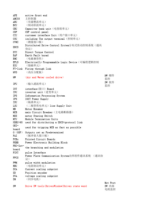
AFE active front endAMC33主控制器ARU(有源整流单元)BCU(制动斩波单元)CBU Capacitor bank unit(电容组单元)CDP CDP control panelCIU customer interface Unit(用户接口单元)COU including The output terminal(控制单元)CVMI(测量接口板)DDCS Distributed Drive Control System分布式传动控制系统(通讯协议)DTC Direct Torque ControlEAF Earth Fault boradEMC(电磁兼容性)EPLD Electrically Programmable Logic Device(可编程逻辑控制EXU(励磁单元)FT-link Firing through linkHVD(高压分配板)HW(Air and Water cooled drive)HW 硬件监控IFU(输入滤波单元)SW 软件监控INT interface(接口) BoardINU inverter unit(逆变单元)IPS Information Processing SystemIPS IGCT Power SupplyISU(隔离单元)LSU(二极管供电单元)line Supply UnitMB Motor BreakerMCB main Circuit Breaker(主电路断路器)MSS motor Staring SwitchMTU Module Termination UnitsNDBU-95uesd for distributing a DDCS-protocol link OEI-boarduesd for tripping MCB as fast as possible O(OSP)Outputs set as PredeterminedPAI(脉冲放大接口板)PCBs Printed Circuit BoardsPEBB Power Electronic Building BlockPEC-Int-boardthe branching and modulationPINT pulse InterfacePPCS Power Plate Communication System功率组件通讯系统 (通讯协议)PWM pulse width modulation RBU(电阻制动单元)SCA Current scaling subprint SD Position encoderSVA voltage scaling subprint SM(同步电机)SW Drive SW tools(DrivesWindow)Drives state word Mot Prot SW 内部电机监控TEU including only the input terminal(终端单元)Mot Wdg Temp SWVLSCD逆变失败监视板Voltage Level&Short Circuit Dectection 通过软件监控,电机绕组的计算温度VLU(电压限幅单元)VSI-MF voltage Source Inverter Multilevel-Fuseless WCU water-cooled(水冷单元)。
LED专业英语[完全整理版网上最全]
![LED专业英语[完全整理版网上最全]](https://img.taocdn.com/s3/m/e065363d650e52ea5518984c.png)
LED照明常用词汇中英文对照11 backplane 背板 2 Band gap voltage reference 带隙电压参考 3 bench top supply 工作台电源 4 Block Diagram 方块图 5 Bode Plot 波特图 6 Bootstrap 自举 7 Bottom FET Bottom FET 8 bucket capacitor 桶形电容 9 chassis 机架 10 Combi-sense Combi-sense 11 constant current source 恒流源 12 Core Saturation 铁芯饱和 13 crossover frequency 交叉频率 14 current ripple 纹波电流 15 Cycle by Cycle 逐周期 16 cycle skipping 周期跳步 17 Dead Time 死区时间 18 DIE Temperature 核心温度 19 Disable 非使能,无效,禁用,关断 20 dominant pole 主极点 21 Enable 使能,有效,启用 22 ESD Rating ESD额定值 23 Evaluation Board 评估板 24 Exceeding the specifications below may result in permanent damage to the device, or device malfunction. Operationoutside of the parameters specified in the Electrical Characteristics section is not implied. 超过下面的规格使用可能引起永久的设备损害或设备故障。
建议不要工作在电特性表规定的参数范围以外。
25 Failing edge 下降沿 26 figure of merit 品质因数 27 float charge voltage 浮充电压 28 fly back power stage 反驰式功率级 29 forward voltage drop 前向压降 30 free-running 自由运行 31 Freewheel diode 续流二极管 32 Full load 满负载 33 gate drive 栅极驱动 34 gate drive stage 栅极驱动级 35 gerber plot Gerber 图 36 ground plane 接地层 37 Henry 电感单位:亨利 38 Human Body Model 人体模式 39 Hysteresis 滞回 40 inrush current 涌入电流 41 Inverting 反相 42 jittery 抖动 43 Junction 结点 44 Kelvin connection 开尔文连接 45 Lead Frame 引脚框架 46 Lead Free 无铅 47 level-shift 电平移动 48 Line regulation 电源调整率49 load regulation 负载调整率 50 Lot Number 批号 51 Low Dropout 低压差 52 Miller 密勒 53 node 节点 54 Non-Inverting 非反相 55 novel 新颖的 56 off state 关断状态 57 Operating supply voltage 电源工作电压 58 out drive stage 输出驱动级 59 Out of Phase 异相 60 Part Number 产品型号 61 pass transistor pass transistor 62 P-channel MOSFET P沟道MOSFET 63 Phase margin 相位裕度 64 Phase Node 开关节点 65 portable electronics 便携式电子设备 66 power down 掉电 67 Power Good 电源正常 68 Power Groud 功率地 69 Power Save Mode 节电模式 70 Power up 上电 71 pull down 下拉 72 pull up 上拉 73 Pulse by Pulse 逐脉冲(Pulse by Pulse) 74 push pull converter 推挽转换器 75 ramp down 斜降 76 ramp up 斜升 77 redundant diode 冗余二极管 78 resistive divider 电阻分压器 79 ringing 振铃 80 ripple current 纹波电流 81 rising edge 上升沿 82 sense resistor 检测电阻 83 Sequenced Power Supplys 序列电源 84 shoot-through 直通,同时导通 85 stray inductances. 杂散电感 86 sub-circuit 子电路 87 substrate 基板 88 Telecom 电信 89 Thermal Information 热性能信息 90 thermal slug 散热片 91 Threshold 阈值 92 timing resistor 振荡电阻 93 Top FET Top FET 94 Trace 线路,走线,引线 95 Transfer function 传递函数 96 Trip Point 跳变点 97 turns ratio 匝数比,=Np / Ns。
多电平变换逆变电路拓扑分析

Telecom Power Technology电力技术应用多电平变换逆变电路拓扑分析汤晖斌(上海杰瑞兆新信息科技有限公司,江苏在众多新兴电子设备诞生后,为了满足其电路使用需求,创建了更为前沿的转换集成电路应用模式,其中最为典型的应用电路就是多电平变换电路。
该电路在应用过程中存在一定的弊病,其中基于电平钳位所引发的逆变电路问题亟需解决。
通过对多电平变换逆变电路拓扑研究背景进行阐述,分析了多种不同的多电平逆变电路拓扑多电平变换逆变电路;拓扑结构;电平钳位Topology Analysis of Multilevel Conversion Inverter CircuitTANG Huibin(Shanghai Jierui Zhaoxin Information Technology Co., Ltd., LianyungangAbstract: After the birth of many emerging electronic devices, in order to meet their circuit requirements, a more advanced application mode of conversion integrated circuits has been created, among which multilevel conversion circuits are the most typical application circuits. In the application process of this circuit, there are also some disadvantages, 2023年6月10日第40卷第11期· 73 ·Telecom Power TechnologyJun. 10, 2023, Vol.40 No.11汤晖斌:多电平变换逆变电路拓扑分析若出现3个以上的电平,则需要增加相同标称值的二极管,从而实现对电平电压的超量处理。
New PWM Control Strategy for Multilevel Three -
To generate the 5-level output current of this converter topology, the switching combination is shown in Table I.
TABLE I.
DIFFERENT SWITCHING COMBINATION
4th International Conference on Power Engineering, Energy and Electrical Drives
Istanbul, Turkey, 13-17 May 2013
New PWM Control Strategy for Multilevel Three Phase Current Source Inverter
M.S. Boucherit
Laboratory of Processus Control .Automatic Department High School of Polytechnic, Alharrach BP182, 10 avenue
Hassen badi. , Algiers, Algeria. ms_boucherit@yahoo.fr
Switching combinations (Sk1Sk4) or (Sk3Sk2 ) or (Sk1Sk2 )or (Sk3Sk4)
Output current 0
Hale Waihona Puke (Sk1) or (Sk3) or (Sk1Sk3Sk4) or (Sk3Sk1Sk2)
I
(Sk1Sk3 )
2I
(Sk2) or (Sk4) or (Sk2Sk3Sk4) or (Sk4Sk1Sk2)
二极管钳位型、混合钳位型三电平逆变器直流侧电容电压平衡问题
基础上增加一个悬浮电容,构造两组双向通 路,实现在高频脉宽调制下两个直流侧电容 和一个悬浮电容电压的动态平衡,进而保证 电容在非理想条件下仍然可以均压,同时在 逆变器软启动时对悬浮电容进行建压。待悬 浮电容的电压上升至直流侧电容电压后,逆 变器开始工作,输出三电平电压。另外,由 于钳位电路的特点,悬浮电容为两个内侧开
图 4 改进型三电平逆变器主电路 Fig.4 Topology of the improved three-level inverter
直流电容电压平衡控制策略的基本思想 为:S1 和 S3 为 a 组开关,S2 和 S4 为 b 组开关; a 组、b 组开关互补导通。在调制波 us 正半周 期内,当 us 大于载波 u1 时,a 组开关导通, b 组开关关断,S1、S3、C1 和 C3 组成双向通 路,实现直流侧电容 C1 与悬浮电容 C3 电压平 衡,当 us 小于载波 u1 时,b 组开关导通,a 组开关关断,S2、S4、C2 和 C3 组成双向通路, 实现直流侧电容 C2 与悬浮电容 C3 电压平衡; 在调制波 us 负半周期内,当 us 大于载波 u2 时, a 组开关导通,b 组开关关断,S1、S3、C1 和 C3 组成双向通路,实现 C2 与 C3 电压平衡, 当 us 小于载波 u2 时,b 组开关导通,a 组开关 关断,S2、S4、C2 和 C3 组成双向通路,实现 C2 与 C3 电压平衡。a、b 两组开关管交替导通 时,就能实现 3 个电容直接或间接的并联, 实现 3 个电容之间动态的电压平衡, vC1=vC2=vC3,满足了三电平逆变器能够正常工 作的 2 个前提:一是悬浮电容电压保持稳定, 二是直流侧分压电容均压。
由于 C1<C2,式(4)、(5)和(6)得到:
tps54386 双路开关电源芯片

MIN
UNIT
2k
1.5k
V
250
PACKAGE DISSIPATION RATINGS(1)(2)(3)
PACKAGE Plastic 14-Pin HTSSOP (PWP)
THERMAL IMPEDANCE JUNTION-TO-THERMAL PAD
(°C/W)
2.07 (4)
TA = +25°C POWER RATING (W)
Voltage • Output Current Up to 3 A • Two Fixed Switching Frequency Versions:
– TPS54383: 300 kHz – TPS54386: 600 kHz • Three Selectable Levels of Overcurrent Protection (Output 2) • 0.8-V 1.5% Voltage Reference • 2.1-ms Internal Soft Start • Dual PWM Outputs 180° Out-of-Phase • Ratiometric or Sequential Startup Modes Selectable by a Single Pin • 85-mΩ Internal High-Side MOSFETs • Current Mode Control • Internal Compensation (See Page 16) • Pulse-by-Pulse Overcurrent Protection • Thermal Shutdown Protection at +148°C • 14-Pin PowerPAD™ HTSSOP package
DK3023_14

∑H V
i =1
i= M
ij i
(14.1)
© 2005 by Taylor & Francis Group, LLC
The equation for the total current flowing in Vi can be written as: Ii =
∑H I
j =1
j=N
ij j
(14.2)
14.1 DC-TO-AC CONVERSION
The Lundell alternator is a source of electrical power to be utilized in most automobiles. The power available is to be utilized during running and in stationary conditions. The role of the battery is very important in this situation. This stored power is utilized as per the needs and requirements in the vehicles. Power conversion and control are performed by power electronic converters that are built by network of semiconductor power switches. For automotive applications, the converters are supplied from DC voltage sources. The basic state of a voltage source converter can be distinguished by the operating states. The input and output terminals are directly connected, cross connected, or separated. The appropriate sequence of states results in conversion of the given input source voltage to the desired output load voltage.
INVERTER原理简介

INVERTER原理简介Inverter 原理简介一、Inverter 的作用Inverter 是一种将DC 转换为AC的器件,用于点亮Panel 背光灯管,其启动瞬间输出约1.1KV- 1.5KV的高压,使冷阴极灯管中的水银蒸发,两电极导通,产生电子,轰击氖气体,产生中子,再轰击水银气体产生紫外线,最后打在荧光粉上而发光,为图像的显示提供背光,正常工作后输出电压约为600V左右,工作电流约在6mA左右。
二、Inverter的基本组成Inverter主要由电压调节器(降压式斩波器)、自激振荡器(多为Royer振荡器)、脉宽调节器PWM IC组成。
INVERTER 基本架构(PWM IC:TL5001)三、电压调节器(降压式斩波器)用于调节供给自激振荡器的电压,从而调节Panel 背光的亮度。
Vo_Von/offR1++L1Vo Vd_输出电压为:V o=Vin*D=Vin*Ton/T(D :负占空比; T on :Q3导通的时间; T :PWM 方波的周期时间)因T 一定,故输出电压V o 与导通时间成正比。
四、 PWM IC (TL5001为例)a.TL5001各脚简要说明PIN1:OUTPUT (输出占空比可调的方波) PIN5:SCP (短路保护)PIN2:VCC (IC 供电) PIN6:DTC (占空比限制)PIN3:COMP (比较器输出) PIN7:RT (振荡器外接电阻)PIN4:FB (反馈) PIN8:GNDTL5001内部结构图Q2TL5001的工作波形五、自激振荡器它是将DC 转换为AC 高压的主要部件。
Vc2Ib1Ib2Vc1Ic1Ic2C1、C2是镇流电容,它使输出电流不会随灯管负载变化而变化很大。
R1、R2作为振荡器的启动电阻,由于晶体管Q1、Q2的特性不同,假设Q1先导通,Ic1慢慢上升(T1的第8脚的电动势为正,Q1维持导通状态,第7脚电动势为负,使Q2截止),上升至Q1完全饱和,此时Ic1不再变化,T1磁通变化量为零,使Q1截止, 产生反向电动势使Q2导通,Ic2慢慢上升,重复上述过程。
Inverter工作原理介绍

Inverter工作原理介绍2007-10-22 09:47Inverter-即逆变器,又叫电压升压板。
它是专为Panel的背光灯提供工作电源的。
Panel使用的背光灯管的工作电压很高,正常工作时的电压为600~800V,而启动电压则高达1500~1800V,工作电流则为5~9mA。
这样的工作特点需要Inverter有如下功能:1)、能够产生1500V以上的高压交流电,并且在短时间内迅速降至800V左右,这段时间约持续1-2S。
2)、由于Inverter提供电流的大小将影响冷阴极荧光灯管的使用寿命,因此输出的电流应小于9mA,需要有过流保护功能。
3)、出于使用的考虑,要有控制功能,即在显示暗画面的时候,灯管不亮。
Inverter是一种DC TO AC的变压器,它其实与Adapter是一种电压逆变的过程。
Adapter是将市电电网的交流电压转变为稳定的12V直流输出,而Inverter 是将Adapter输出的12V直流电压转变为高频的高压交流电;两个部分同样都采用了目前用得比较多的脉宽调制(PWM)技术。
其核心部分都是一个PWM集成控制器,Adapter用的是UC3842,Inverter则采用TL5001芯片。
TL5001的工作电压范围3.6~40V,其内部设有一个误差放大器,一个调节器、振荡器、有死区控制的PWM发生器、低压保护回路及短路保护回路等。
以下将对Inverter的工作原理进行简要介绍:Inverter工作原理框图输入接口部分:输入部分有3个信号,12V直流输入VIN、工作使能电压ENB及Panel电流控制信号DIM。
VIN由Adapter提供,ENB电压由主板上的MCU提供,其值为0或3V,当ENB=0时,Inverter不工作,而ENB=3V时,Inverter处于正常工作状态;而DIM电压由主板提供,其变化范围在0~5V之间,将不同的DIM值反馈给PWM控制器反馈端,Inverter向负载提供的电流也将不同,DIM值越小,Inverter输出的电流就越大。
CPS-SPWM调制技术研究及其FPGA实现--毕业设计

安徽工业大学毕业设计(论文)任务书毕业设计(论文)的主要内容:1.学习电力电子技术的主要内容。
2.研究CPS-SPWM技术的原理。
3.设计一种完全基于FPGA的CPS-SPWM调制波形产生的方案。
4.完成对系统的软硬件测试。
起止时间:2010年3月5日至2010年6月1日共14周指导教师签字系主任签字院长签字摘要在分析了多电平逆变原理的基础上,分别对双极性CPS-SPWM和单极倍频CPS-SPWM的调制原理和输出波形进行了严密的公式推导和理论分析。
在比较了几种CPS-SPWM调制脉冲产生方案后,为了解决一些存在的问题,提出了一种完全由FPGA 产生CPS-SPWM调制波的设计方案,并在EP1C6上实现了基于该方案的调制波形发生模块。
该模块可产生三相共60路CPS-SPWM调制波形,使用该模块产生的调制波形控制三相五级全桥式逆变器,可产生多达11电平的输出正弦波。
设计加入了多样化设计,可通过用户接口进行电平数、调制度、载波比等参数设置。
通过优化设计,节省了芯片资源,提高了芯片效率。
仿真和实验证明了该设计的可行性。
关键词:电力电子;多电平变换器;载波移相SPWM发生器AbstractAfter thoroughly analyzing the generation principle of multi-level converter, theortical analysis of modulating principle and output voltage waveform of bipolar CPS-SPWM and single pole double frequency CPS-SPWM is done. There are a few methods now, they have their advantage and disadvantage, in order to solve the drawback, a whole new method to generate multipath SPWM by FPGA completely is proposed, which is realized in Altera FPGA. This generator may produce 60-way SPWM waveform and adjust the amplitude and the frequency of the SPWM waveform. A multi-level inverter with 3 phase can be modulated by these waveform. The very output waveform of this inverter is a 11-level sine wave. By means of the optimum design, the chip resources is saved and the chip efficiency is enhanced. The simulative and experimental results proved the feasibility of the design.Keyword: Power electronics; Multilevel-converter; Carrier phase shifted SPWM generator目录1 绪论 (1)1.1 逆变技术概述 (1)1.2 多电平逆变技术概述 (2)1.2.1 多电平逆变器的结构 (2)1.2.2 多电平逆变器的输出 (2)1.2.3 多电平逆变器的控制 (3)1.3 本课题的意义和任务 (3)2 CPS-SPWM技术研究 (4)2.1 CPS-SPWM技术概述 (4)2.2 载波相移SPWM(CPS-PWM)理论 (5)2.2.1 双极性CPS-SPWM (5)2.2.2 单极倍频CPS-SPWM (10)2.3 结论 (15)3 基于FPGA的CPS-SPWM脉冲产生设计方案 (16)3.1 主控器件的选择 (16)3.2 单相脉冲发生模块设计 (17)3.3 三相脉冲发生结构设计 (18)4 基于FPGA的CPS-SPWM脉冲发生模块的实现 (19)4.1 单相各模块的实现 (19)4.1.1 系统复位及时钟分频模块 (19)4.1.2 正弦波/三角波ROM表 (21)4.1.3 三角波/正弦波地址累加器 (23)4.1.4 正反相调制比较器 (25)4.1.5 死区控制模块 (27)4.1.6 正弦调制波的幅频控制 (29)4.1.6 单相仿真 (30)4.2 三相集成 (31)4.2.1 B相、C相的设计 (31)4.2.2 顶层设计 (32)4.3 实验调试 (33)4.3.1 实验平台 (33)4.3.2 调试工具 (34)4.3.3 相关测试 (35)5 结论 (38)致谢 (38)参考文献 (38)1 绪论1.1 逆变技术概述通俗的说,逆变技术就是把直流电变为交流电的技术。
- 1、下载文档前请自行甄别文档内容的完整性,平台不提供额外的编辑、内容补充、找答案等附加服务。
- 2、"仅部分预览"的文档,不可在线预览部分如存在完整性等问题,可反馈申请退款(可完整预览的文档不适用该条件!)。
- 3、如文档侵犯您的权益,请联系客服反馈,我们会尽快为您处理(人工客服工作时间:9:00-18:30)。
A Multilevel Current-Source Inverter BasedGrid-Connected Photovoltaic System Prajna Paramita Dash,Student Member,IEEE,Mehrdad Kazerani,Senior Member,IEEEAbstract—This paper proposes a grid-connected Photovoltaic (PV)system based on a multilevel Current Source Inverter (CSI)topology.The topology proposed here consists of parallel-connected CSI modules operating at a very low switching fre-quency.For n number of inverter modules,2n+1current levels are resulted in the output.In the multilevel inverter topology, each inverter module has its own PV source,Maximum Power Point Tracking(MPPT)unit,and DC-link current controller. Unlike earlier proposed multilevel CSI topologies,the proposed topology has a single AC-side current controllers,lowering the requirements for AC-side sensors andfilters.To demonstrate the performance of the multilevel inverter based on CSI,two inverter units are considered in this study.The simulation studies are carried out in PSCAD/EMTDC environment.Index Terms—Current-Source Inverter(CSI),multilevel,Max-imum Power Point Tracking(MPPT),feed-forward,Insolation level,Control.I.N OMENCLATUREv s:CSI AC-side terminal voltagev:V oltage at the PCC,voltage at the secondary side of transformer,T re:Substation bus(Grid)voltagev dc:DC-side voltage of the CSIv pv:V oltage of the PV arrayi pvn:PV array currenti dcn:DC-link current of the CSIi tn:CSI AC-side terminal currenti c:Current through thefilter capacitori s:Current injected into the gridP pv:PV array powerP s:Real power delivered by the PV system to the gridQ s:Reactive power delivered by the PV system to the grid N:Interface transformer T r turns ratioC f:Filter capacitanceR g:Resistance of the distribution lineL g:Inductance of the distribution lineω:dq-frame angular speedω0:Nominal angular frequency of grid(e.g.,377rad/s for 60Hz)δ:dq-frame reference angleS:Insolation/irradiation levelRe{}:Real part of{}Im{}:Imaginary part of{}d:Subscript denoting d-axis componentq:Subscript denoting q-axis component:Symbol denoting space-phasor quantityAuthors are with the University of Waterloo,Waterloo,ON,Canada.(e-mail:ppdash@engmail.uwaterloo.ca and mkazeran@ecemail.uwaterloo.ca) :Symbol denoting peak value of a three-phase variable T:Superscript denoting matrix transpositions:Complex frequency,σ+jωII.INTRODUCTIONMultilevel inverters have drawn tremendous attention in recent years and have been studied for high-voltage and high-power applications.By increasing the number of levels in a given topology,the output voltage in case of VSI,and output current in case of CSI,assume stair-case waveforms with higher number of steps compared to single-stage,this results in a close-to-sinusoidal waveform with a reduced Total Harmonic Distortion(THD)at reduced switching frequency. Moreover,operation of multilevel inverter at low switching frequency results in lower switching loss and higher power transfer capability.For their advantageous features,multilevel inverters have been adopted in Distributed Generation(DG) application.Multilevel inverter based on V oltage-Source In-verter(VSI)has been studied and implemented more ex-tensively as compared to other power electronic converter topologies.The thoroughly researched VSI-based multilevel inverters can be categorized into Neutral Point Clamped(NPC) inverter,Flying Capacitor(FC)inverter,Cascade full bridge inverter and the recently-introduced Hybrid and Hexagram Inverter[1].Though VSI is the dominant topology in DG application,it has some drawbacks such as shorter lifetime of the DC-link capacitor and inherent buck characteristics.There-fore,researchers and manufacturers have started investigating for an efficient topology.The topology which has attracted considerable attention is the Current Source Inverter for its inherent boost characteristics,longer lifetime of the storage unit,inherent fault protection capability,and direct control of the output current[2][3].The reason behind CSI not being as popular as VSI is that inductors used in CSI as storage elements have higher conduction losses and thus lower energy storage efficiency compared to DC-link capacitors of VSI [4][5].However,with the development of Superconducting Magnetic Energy Storage(SMES)technologies the problem associated with conventional inductors are going to be solved and hence CSIs can be considered appropriate for high power application[6].Moreover,the recently-introduced RB-IGBT (Reverse Blocking Insulated Gate Bipolar Junction Transistor) has eliminated the need for series diode and thus making CSI a lucrative alternative.Recently,the interest of researchers for multilevel inverters based on CSI for various applications has noticeably increased.Most of the multilevel CSIs reported in the literatures to date have been based on a single-phase cell[7][10],basicallyvariations of the generalized multicell structure proposed in[11].The generalized structured proposed in[10]has beenextended to a three-phase topology in[12].The topologyproposed in[12]is a three-phase5-level CSI that uses only twointermediate DC-link inductors and a single DC current source.A modified three-phase multicell CSI topology is proposedin[13].The topology proposed in[13]is different from theearlier proposed topologies in terms of number of currentlevels.The levels of current produced by multicell CSI in[12]is2n+1compared to2n−1produced by others,where n isthe number of CSIs employed.The work presented in[7]-[12]mainly revolves around modulation strategy and switching.Moreover,the analysis carried out in the aforementionedliteratures is based on the assumption that there is an idealcurrent source in the input.A closed-loop control strategyis proposed in[15]for afive-level CSI.However,the mainpurpose for the control strategy is to ensure even distributionof current between the two inverters.Control algorithm formultilevel CSI is not well investigated as in the case of VSI.Lack of research in thefield of control strategy for a multilevelCSI and application of CSI-based multilevel in DG are themotivation behind the study presented in this paper.The multilevel CSI under study in this paper consists of nnumber of CSIs connected in parallel capable of producing 2n+1levels of output current.Each inverter unit is energized from its own PV source.The current from each PV arrayis independently controlled by DC-link controller,whereasa combined control scheme is implemented for the AC-sidecurrent.The topology employed in this paper is capable ofaccommodating PV sources operating under equal and variedinsolation levels.Moreover,the proposed CSI-based multileveltopology is an efficient structure in terms offilter and sensors. The rest of the paper is organized as follows.Section III presents a detailed single-line schematic diagram of the mul-tilevel CSI for PV system application.The control strategy for the multilevel CSI and performance analysis of the complete system are presented in Section IV and V,respectively.Finally Section VI concludes the paper.III.S TRUCTURE OF THE PV S YSTEM B ASED ONM ULTILEVEL C URRENT-S OURCE I NVERTERFig.1presents single-line schematic diagram of the pro-posed grid-connected PV system based on multilevel CSI.DC-link current of each inverter unit is controlled independently, whereas control of AC-side current is performed according to a combined current control scheme.Each PV system is operating at the maximum power by their own Maximum Power Point Tracker(MPPT).Each PV array is interfaced with the corresponding inverter through DC-link inductor L dc. The AC-side of the multilevel inverter is interfaced to a three-phase transformer,T r through a capacitivefilter C f. The secondary side of the transformer T r is connected to grid through resistance,R g and inductance,L g.A load is situated on the secondary side of the transformer.The load is an induction machine.Breaker B r is provided by the utility,whereas B pv is part of the multilevel inverter-based PV system.The purpose of breaker B pv is to prevent the multilevel inverter-based PV system from islanding when there is any abnormal condition in the utility side.For the purpose of study, the grid is assumed to be a stiff grid.The proposed multilevel structure with control scheme is capable of operating equal and unequal insolation/irradiation level.To demonstrate the dynamic performance it is considered that the PV units are operating under equal insolation level for this paper.The mul-tilevel inverter presented in Fig.1is operated based on Phase-Shifted Carrier Sinusoidal Pulse Width Modulation strategy. Since,the number of inverters employed in the multilevel inverter structure is two,the carrier signals are phase shifted by 3600/2=1800.Fig.2demonstrates the multilevel operation of the system presented in Fig.1.IV.C ONTROL STRUCTURE FOR THE PV SYSTEM BASED ON MULTILEVEL C URRENT-S OURCE I NVERTERThe controller of a grid-connected CSI-based PV system is expected to control the DC-and AC-side currents to ensure: (i)a high-quality sinusoidal current from all the inverters is injected into the grid,(ii)the real power injected into the grid is equal to the summation of maximum power that can be extracted from the PV panel under all conditions, and(iii)the reactive power at the interface with the grid assumes the desired value.As illustrated by Fig.1,the Pulse Width Modulation(PWM)and control of the CSI need to be synchronized to the grid voltage through a Phase-Locked Loop (PLL).Fig.1also shows that the error signals between the reference commands,i sdref1and i sdref2from two inverters and i sqref are processed by two PI controllers to generate the modulating signals,m d and m q.Even though the PI controller is simple in structure and easy to implement,proper tuning of its parameters requires adequate insight.An intuitive method for tuning of the PI controller parameters is proposed in this section.A.Phase-Locked-Loop(PLL)To simplify the control structure,the AC variables of the PV system are projected on a dq frame which is rotating at an angular speedω.In steady state,the AC variables are sinusoidal functions of the grid frequency,ω0.If the dq-frame angular speed is adjusted to the grid frequency,the transformed quantities become time-invariant in steady-state,simplifying the controller design.This is achieved by means of a Phase Locked Loop(PLL)[16],whose block diagram is given in Fig.3.Thefigure shows that the input to the PLL block is the sinusoidally-varying voltage from the Point of Common Coupling(PCC)and the output is the angle for abc-to-dq and dq-to-abc transformations,δ.The voltage v s is resolved into d-and q-axis components based on[17].In Fig.3the voltage v sq is regulated to zero using a PI controller,H(s).Regulating q-axis component of the voltage to zero makes the active and reactive powers,P s and Q s,independent of the voltage v sq [17].Therefore,active power,P s and reactive power,Q s can be expressed in terms of currents i sd and i sq as:P s=32v sd i sd.(1)Fig.1.Single-line schematic diagram of the three-phase,multi-level,grid-connected PV system based on CSIFig.3.Block diagram of the Phase-Locked Loop (PLL)Hence,P s is proportional to,and can be controlled by,i sd .Similarly,the dq -frame expression for the reactive power takes the form:Q s =−32v sd i sq .(2)Equation (2)indicates that Q s can be controlled by i sq .B.Design of Inner Current Control LoopEquations (1)and (2),respectively,show that active and reactive powers delivered by the CSI can be adjusted by controlling i sd and i sq ,respectively.Fig.4shows the blockdiagram of the CSI AC-side current controller.Controller structures k d (s )and k q (s )in Fig.4are expressed as:k d (s )=k q (s )=k p +k is(3)where k p nd k i are the proportional and integral gains,respectively.Control signals m d and m q are obtained asm d =i tdref i dc and m q =i tqrefi dc(4)where i tdref and i tqref are current references derived from the outputs of the compensators k d (s )and k q (s ),respectively.The d -axis component of the inverter output current,i td ,is related to the current i sd as:i td =i cd +i sd(5)where i cd is d -axis component of the filter capacitor current.It should be noted that with a proper filter design,the fundamental-frequency component of the capacitor current will be very small,i.e.,i cd is negligible as compared to i sd .The same discussion can be made for the q -axis components.Fig.2.Phase-Shifted Carrier Sinusoidal Pulse Width Modulation(SPWM)(a)Carrier signals;(b)Modulating Signals;(c)Terminal current offirst inverter;(d)Terminal current of second inverter;(e)Multilevel ouput current outputTherefore,one can writei td≈i sd≈m d i dc and i tq≈i sq≈m q i dc(6)iisdFig.4.Block diagram of the CSI AC-side current control systemUnder the assumption that i cd=0,the following transferfunction can be written for the closed-loop control system ofi sd illustrated in Fig.4.T(s)=i sdi sdref=k p+K isk p+k i s+1=s k pk p+1+k ik p+1s+k ik p+1(7)As the value of k p increases the pole of the transfer function T(s)in(7)approaches the origin of s-plane,which is not desirable.Therefore,to imitate the transient behavior of afirst-order system,k p should be chosen to be small.k i,as the inverse of time-constant,τi is chosen in the range of0.5ms to5ms to get a fast and accurate response.Thus,k p and k i can be written as:k p≈0and k i=1τi(8) andSubstituting the values of k p and k i in(7)the transfer function T(s)becomesT(s)=i sdi sdref1+i sdref2=1τis+1τi=1τi s+1(9)C.Design of Outer Current Control LoopSince,the outer current controller structures of two inverters are similar,a detailed control structure of the top inverter is described in the following sections.The outer controller of the CSI is designed based on the equation:12L dcdi2dc1dt=P pv1−32(v sd i sd+v sq i sq)(10) where P pv is the power delivered by the PV array.Equation (10),after substituting v sq=0,represents a system with i sd as the input,i2dc the output and v sd the disturbance input. If time constantτi in the PI compensator of the current controller is properly selected,i sd can be approximated to i sdref.Therefore,(10)can be rewritten as:12L dcdi2dc1dt≈P pv1−32v sd i sdref1(11)2dc2i 2dc1Fig.5.Control Structure of multilevel CSI-based PV systemThe DC-link current controller designed on the basis of (11)is illustrated in Fig.5.According to 11,the fact that P pv is product of v pv and i dc makes the system nonlinear.To mitigate the impact of nonlinearity,i sdref can be derived in the following way:i sdref =u i +η P pv 132v sdi ff 1(12)where u i is a new control input,shown in Fig.5,and i ff is a feed-forward signal that can be enabled or disabled when the binary multiplier ηassumes the value unity or zero.Substituting for i sdref from (12)in (11),one getsL dc 2di 2dc 1dt ≈(1−η)P pv 1−32v sd u i .(13)Equation (13)indicates that if η=1,the impact of the PV array nonlinearity on the DC-side current control is eliminated,and the effective control unit becomes an integrator.V.S IMULATION R ESULTSFig.6presents the response of the PV system based on multilevel CSI due to a step change in insolation level.The simulation is carried out in PSCAD/EMTDC environment [18].At t =1s insolation level is changed from 0.8kW/m 2to 1kW/m 2,as shown in Fig.6(a).Due to change in insolation level,current references from the MPPTs increase,which in turn increases the multilevel CSI terminal current,as illustrated in Fig.6(b).With the change in reference values from MPPT,the output from DC-link controller increases,which causes a change in the current that is injected into the grid,as shown in Fig.6(c).Currents i sdq represents the d -axis and q -axis component of the current i s .In order to maintain unity power factor at the Point of Common Coupling (PCC),q -axis component of the current i s is regulated to zero byFig.6.Response of the PV system to a step change in insolation level (a)Insolation level;(b)Multilevel current at the terminal of the multilevel inverter;(c)d -and q -axis currents injected into the grid;(d)V oltage and current the Point of Common Coupling (PCC)the AC-side current controller,as shown in Fig.6(c).Fig.6(d)shows that a clean sinusoidal current results from the multilevel inverter-based PV system and unity power factor is maintained at the PCC.VI.C ONCLUSIONThe paper presented the structure for the power circuit and control system for a multilevel inverter system for three-phase,grid-connected PV application.The porposed structures differs from those proposed earlier in terms of control structure and use of independent DC current sources.Each inverter unit has independent MPPT and DC-link controllers.Independent operation of PV units allows accommodating PV units underdifferent insolation levels.The DC-link current controller employs a feed-forward control strategy.Each DC-link current controller contributes the generation of reference signals for the AC-side current controller.In this paper,simulation results for PV systems operating under equal insolation levels were presented.On the AC-side of the inverter a combined current control in dq-frame is implemented.The current controller ensures that the PV system is operating at unity power factor. Moreover.high quality waveforms are generated at a low switching frequency and with inexpensive capacitivefilter common to all modules.In addition,the proposed structure avoids use of individual current sensors at the AC outputs of all modules.VII.A PPENDIX:S YSTEM P ARAMETERS Parameters for the PV system,line and induction machine are presented in Table I.TABLE IS YSTEM P ARAMETERSPV System Parameter Value CommentsGrid inductance,L g1mhGrid Resistance,R g1mΩGrid voltage,v g 6.6kVT r nominal power 2.6MV AT r voltage ratio 6.6/0.48kV Y/Delta T r leakage inductance0.1puT r ohmic resistance0.02puon-state resistance of valves3mΩvalves resistance,R 3.0mΩfilter capacitance,C f500μFswitching frequency300Hz51×60HzDC-link capacitance,C5000μFDC-link inductance,L dc1mH#of PV cells per string,n s1500#of PV strings,n p176ideality factor,A 1.92cell reference temperature,T r300Ktemperature coefficient,kϑ0.0017A/Kcell short circuit current,I scr8.03Areverse saturation current,I rs1.2×10−7AController Parameter Value Commentsk p(forτi=0.5ms)0.0002Ωk i(forτi=0.5ms)2Ωs−1Line Parameter Value Commentsgrid voltage 6.6kV rms l−l line inductance,L1+L20.105mH per kmX/R ratio0.6line resistance based on L&X/Rline length,l e15kmLoad Parameter Value Commentsnominal power373kV Anominal voltage 6.6kV rms l−lnominal frequency60Hzrotor/stator turns ratio 1.0stator resistance,R s0.0184purotor resistance,R r0.0132pumagnetizing inductance,L m 3.8pustator leakage factor,σs0.0223rotor leakage factor,σr0.0223inertia constant,H 2.1smechanical damping,D0.135puR EFERENCES[1]N.Vazquez,H.Lopez,C.Hernandez,E.Vazquez,R.Osorio,and J.Arau,A Different Multilevel Current-Source Inverter,IEEE Transactions on Industrial Electronics,vol.57,no.8,pp.2623-2632,2010.[2]Z.Bai,Z.Zhang,and Y.Zhang,A Generalized Three-Phase MultilevelCurrent Source Inverter with Carrier Phase-Shifted SPWM,in2007IEEE Power Electronics Specialists Conference,pp.2055-2060,2007.[3]Y.Xiangwu,Z.Bo,G.Xiaobin,Z.Lixia,and Li Heming,Double Closed-loop Control of Three-Phase Five-level PWM Current Source Inverter,in IECON2007-33rd Annual Conference of the IEEE Industrial Electronics Society,pp.2110-2114,2007.[4]P.E.Melin,J.R.Espinoza,N.R.Zargari,L.A.Moran,and J.I.Guzman,A novel multi-level converter based on current source power cell,in2008IEEE Power Electronics Specialists Conference,pp.2084-2089,2008.[5]Z.Zhang and B.Ooi,Multi-modular current-source SPWM converters forsuperconducting magnetic energy storage system,in PESC‘92Record.23rd Annual IEEE Power Electronics Specialists Conference,pp.561-568.[6]J.Espinoza,L.Moran,and N.Zargari,Multi-Level Three-Phase CurrentSource Inverter based Series Voltage Compensator,in IEEE36th Confer-ence on Power Electronics Specialists,2005.,pp.2264-2269.[7]Zhong Du,L.Tolbert,and J.Chiasson,Active harmonic elimination formultilevel converters,IEEE Transactions on Power Electronics,vol.21, no.2,pp.459-469,2006.[8]M.Liserre,V.G.Monopoli,A.Dell’Aquila,A.Pigazo,and V.Moreno,Multilevel Phase-Shifting Carrier PWM Technique in case of Non-Equal dc-Link Voltages,in IECON2006-32nd Annual Conference on IEEE Industrial Electronics,pp.1639-1642,2006.[9] D.Xu and B.Wu,Multilevel Current Source Inverters with PhaseShifted Trapezoidal PWM,in IEEE36th Conference on Power Electronics Specialists,2005.,pp.2540-2546.[10]M.Dahidah,and V.G.Agelidis Selective Harmonic Elmination Multi-level Converter control with Variant DC sources,in ICIEA‘09Record.Annual Industrial Electronics and Application,2009,pp.3351-3356. [11]P.Enlin,J.Espinoza,N.Zargari,and J.I.Guzman A Novel Multi-LevelConverter based on Current Power Cell,in PESC‘08Record.Annual IEEE Power Electronics Specialists Conference,pp.2084-2089. [12]M.C.Chandorkar,D.M.Divan,and sseter,Control Techniquesfor Multiple Current Source GTO Converters,IEEE Transactions on Industry Application,vol.31,no.1,pp.134-140,1995.[13]S.H.Hosseini,M.Kangarlu A New Topology for Multilevel CurrentSource Inverter with Reduced Number of Switches,in ELECO‘09Record.Electrical and Electronics Engineering Conference,pp.273-277. [14]Z.Bai,Z.Zhang,and Y.Zhang A Generalized Three-Phase MultilevelCurrent Source Inverter with Carrier Phase-Shifted SPWM,in PESC ‘07Record.Annual IEEE Power Electronics Specialists Conference,pp.2055-2060.[15]Y.Xu,L.Xin,and Z.Zhang A New Three-phase Five-level Current-Source Inverter,in Applied Power Electronic Conference,2005.,pp.424-427.[16]S.K.Chung,“A phase tracking system for three phase utility interfaceinverters,”IEEE Transactions on Power Electronics,vol.15,no.3,pp.431-438,May2000.[17] A.Yazdani,P.P.Dash,A control methodology and characterization ofdynamics for a Photovoltaic(PV)system interfaced with a distribution network IEEE Transaction on power delivery,vol.24,no.3,pp.1538-1551,July2009.[18]PSCAD/EMTDC,v.4.2Manitoba HVDC Research Centre,Winnipeg,Manitoba,Canada。