EMIF2MIC68FCC中文资料
美奇 Micrel MIC4478 79 80 低压双尖极电流控制驱动器说明书

MIC4478/79/80 Evaluation Board32V Low-Side Dual MOSFET DriversGeneral DescriptionThe MIC4478, MIC4479, and MIC4480 are low-side dualMOSFET drivers. They are designed to switch N-channelenhancement type MOSFETs from TTL-compatible controlsignals for low-side switching applications. The MIC4478 isdual non-inverting, the MIC4479 is dual inverting, and theMIC4480 has complimentary non-inverting and invertingdrivers. Short propagation delays and high peak currentsproduce precise edges and rapid rise and fall times. TheMIC4478/4479/4480 are powered from a +4.5V to +32Vsupply voltage. The on-state gate drive output voltage isapproximately equal to the supply voltage (no internalregulators or clamps). In a low-side configuration, thedrivers can control a MOSFET that switches any voltageup to the rating of the MOSFET. The MIC4478/4479/4480are available in an 8-lead SOIC (ePAD and non-ePAD)package and rated for –40°C to +125°C ambienttemperature range.Data sheets and support documentation are available onMicrel’s web site at: .Evaluation Board DescriptionControl IC ............................... MIC4478/MIC4479/MIC4480Topology ......... Dual Low-Side MOSFET Driver with EnableV DD Supply Voltage Range(1)............................. 4.5V to 32VMaximum Input Pin Voltage ........................................... V DDMaximum Enable Pin Voltage ........................................ V DDMaximum External FET Supply Voltage (V IN) (100V)Note:1. V DD must be less than 18V so as not to exceed the maximum FETV GS rating.Features•External MOSFETs on the board to simplify testing.•Resistor and capacitor component locations on thedriver outputs for ease of testing.RequirementsThe evaluation board requires:• A V DD power supply with an output between 4.5Vand 32V to power the driver. While the driver canoperate up to 32V, do not exceed 18V when usingthe MOSFETs that come with this evaluationboard.•An external V IN supply voltage for powering theMOSFET drains. Do not exceed the 100V V DSrating of the MOSFETs.Precautions•Ensure the V DD supply does not exceed themaximum V GS of the MOSFETs being used.V GS(ABS_MAX) for the MOSFETs that come with theevaluation board is 20V. 18V maximum isrecommended.•The evaluation board does not have reversepolarity protection. Applying a negative voltage toV DD or V IN may damage the device. Do not exceed32V on the input, nor exceed the MOSFET’sV GS(MAX) to prevent damage to the driver andMOSFETs. Do not exceed 100V on either of thetwo DRAIN_A or DRAIN_B terminals.Ordering InformationPart Number DescriptionMIC4478YML EV MIC4478YML Evaluation BoardMIC4479YML EV MIC4479YML Evaluation BoardMIC4480YML EV MIC4480YML Evaluation BoardGetting Started1. Connect the V DD and GND terminals to an externalsupply voltage. The input voltage range is from 4.5V to 18V. The 18V maximum is limited by the V GS of theMOSFETs.2. Apply a square wave or pulse to the INA and/or INBterminals. The logic 0 level is less than 0.8V and thelogic 1 level is greater than 2.4V. Do not exceed V DDon the inputs. Headers TP1 and TP4 may be used toapply or monitor the input signal.3. The output signal can be monitored with a scopeprobe at the OUT_A and OUT-B pins. Headers TP3and TP6 may also be used to monitor the outputsignals.ENA and ENB InputsThe ENA and ENB inputs are each accessible through a 3-pin header. The EN pins are internally pulled up and do not need a jumper or external signal for the outputs to be enabled. The outputs can be individually disabled with a low signal or a shorting jumper connected from EN to ground. Headers JP2 and JP3 can be used to apply or monitor the enable signals.INA and INB InputsThe output drivers are controlled by the INA and INB signal. Table 1to shows the output state based on the input for each of the three drivers. Do not leave the inputs floating when V DD is applied.Table 1. Input ConfigurationDevice INA(Pin 2)INB(Pin 4)OUTA(Pin 7)OUTB(Pin 5)MIC4478 L/H L/H L/H L/HMIC4479 L/H L/H H/L H/LMIC4480 L/H L/H H/L L/HOUTA and OUTB OutputsThe evaluation board allows the option of driving a MOSFET or capacitance. The board is populated with a 100V N-channel MOSFET to show “real world” operation. The MOSFET may be removed and a capacitor used if standardized testing is needed. Capacitor locations C3 (OUT_A) and C6 (OUT_B) may be used for capacitive testing.Resistor locations R4 and R9 allow a resistor to be placed in series with the driver output. The board comes with the resistor pads shorted with etch. The etch between the pads of the resistor must be cut before a resistor is added. External MOSFETsA pair of 100V MOSFETs are included with the board to facilitate testing of the driver. Terminals are provided for an external supply. A 1kΩresistor is connected in series between each of the supply inputs and MOSFET drains. This limits the current flowing through the MOSFETs and allows the switching waveform to be observed. These resistors may be changed or removed, depending on the application. A 4.7µF capacitor, from the supply terminal to ground, is provided for decoupling the high frequency switching currents. The capacitors and MOSFETs are rated to 100V.Evaluation Board SchematicJ1V J3J14J4INA J11INBJ12GND J7DRAIN_BBill of MaterialsItem Part Number Manufacturer Description Qty. C1 C1608X7R1H104K080AA TDK(2)0.1µF Ceramic Capacitor, 50V, X7R, Size 0603 1 C2, C7 C3126X5R1H105K160AA TDK 1µF Ceramic Capacitor, 50V, X5R, Size 1206 1 C3, C6 Open Location, Size 0603 2 C4, C5 C3225X7S2A475M200AB TDK 4.7µF Ceramic Capacitor, 100V, X7S, Size 1210 2 Q1, Q2 AM4492N Analog Power(3)100V, N-Channel MOSFET, SOIC-8 2 R1, R2, R4,R5b, R6,R7b, R8, R9Open Location, Size 0603 8 R5, R7 CRCW12061001FRT1 Vishay(4)1kΩ Resistor (1206 size), 1% 2U1 MIC4478YMEMicrel, Inc.(5)32V Low-Side Dual MOSFET Driver 1 MIC4479YMEMIC4480YMENotes:2. TDK: .3. Analog Power: .4. Vishay: .5. Micrel, Inc.: .PCB Layout RecommendationsTop LayerBottom LayerMICREL, INC. 2180 FORTUNE DRIVE SAN JOSE, CA 95131 USATEL +1 (408) 944-0800 FAX +1 (408) 474-1000 WEB Micrel, Inc. is a leading global manufacturer of IC solutions for the worldwide high performance linear and power, LAN, and timing & communications markets. The Company’s products include advanced mixed-signal, analog & power semiconductors; high-performance communication, clock management, MEMs-based clock oscillators & crystal-less clock generators, Ethernet switches, and physical layer transceiver ICs. Company customers include leading manufacturers of enterprise, consumer, industrial, mobile, telecommunications, automotive, and computer products.Corporation headquarters and state-of-the-art wafer fabrication facilities are located in San Jose, CA, with regional sales and support offices and advanced technology design centers situated throughout the Americas, Europe, and Asia. Additionally, the Company maintains an extensive networkof distributors and reps worldwide.Micrel makes no representations or warranties with respect to the accuracy or completeness of the information furnished in this datasheet. This information is not intended as a warranty and Micrel does not assume responsibility for its use. Micrel reserves the right to change circuitry, specifications and descriptions at any time without notice. No license, whether express, implied, arising by estoppel or otherwise, to any intellectual property rights is granted by this document. Except as provided in Micrel’s terms and conditions of sale for such products, Micrel assumes no liability whatsoever, and Micrel disclaims any express or implied warranty relating to the sale and/or use of Micrel products including liability or warranties relating to fitness for a particular purpose, merchantability, or infringement of any patent, copyright, or other intellectual property right.Micrel Products are not designed or authorized for use as components in life support appliances, devices or systems where malfunction of a product can reasonably be expected to result in personal injury. Life support devices or systems are devices or systems that (a) are intended for surgical implant into the body or (b) support or sustain life, and whose failure to perform can be reasonably expected to result in a significant injury to the user. A Purchaser’s use or sale of Micrel Products for use in life support appliances, devices or systems is a Purchaser’s own risk and Purchaser agrees to fullyindemnify Micrel for any damages resulting from such use or sale.© 2015 Micrel, Incorporated.。
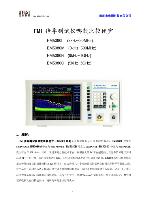
EMI传导测试仪哪款比较便宜
频率范围/MHz
0.15-0.5 0.5-5 5-30
限值/dBuV
准峰值(QP)
平均值(AV)
66-56
56-46
56
46
60
50
①绘制 QP 曲线 Limit Name 填入标准名称“EN55022”,单位选择 dBuV. 点选“QP”。 在 Freq 输入相应频率, Amplitude 输入限值,然后选择 Add ,也可以 Delete 删除,或者 Reset 全
选择所需标准并确定。如需添加新标准可参考”如何绘制标准曲线”。
选择补偿曲线。实际的应用中,在被测信号接入到接收机之前通常会有 LISN,天线,CDN,限幅器, 衰减器以及线缆等仪器设备,所以必须进行相关损耗补偿,可通过添加补偿曲线进行修正。如果没有 所需的补偿值可手动绘制补偿曲线,具体方法参考“如何绘制补偿曲线”。
12
深圳市优测科技有限公司
③绘制 PK 曲线 绘制 PK 曲线与绘制 QP 曲线方法相同。绘制完 PK 曲线点 Save。然后 Exit 曲线标准绘制完毕。例如
汽车电子 GB18655CISPR 25 L3 标准中有需要绘制 AV,QP,PK 三条曲线的。
绘制和调用补偿曲线
说明 复位软件到初始状态 在扫描运行过程中不要进行相关设置工作,在停止后进行设置 可以对扫描的数据进行编辑,包括峰值查找,添加和删除频点等 可以对数据表中的频点进行终测测试 快速生成检测报告 进入 Spot 模式,单点测量 返回上一级菜单
表 5:接收机软件主界面
接收机模式快速操作步骤
①Scan 扫描测试设置和测试
前置放大器开启
30MHz<f<1GHz,带宽 120kHz < 0dBμV
llcc68中文技术手册
llcc68中文技术手册LLCC68是一款廉价、低功耗、高性能的单片机,可以广泛应用于各种嵌入式系统中。
以下是LLCC68的技术手册:1. 架构LLCC68采用ARM Cortex-M4内核,频率可以高达168MHz,支持DSP指令集和浮点运算。
它还具有256KB的Flash存储器和64KB的SRAM存储器,以及丰富的外设功能,如多种通信协议、模拟输入/输出、数字协议等。
2. 基本功能LLCC68支持多种通信协议,如I2C、SPI、UART等。
它还包括DMA 控制器、时钟、复位控制器和电源管理单元等基本功能。
此外,LLCC68具有一组GPIO引脚,使其能够与其他设备进行通信。
3. 时钟和计时器LLCC68内置了各种时钟和计时器,包括系统时钟、控制器时钟和计时器等。
LLCC68还支持超低功耗模式,使其非常适合于需要长时间运行的应用程序。
4. 模拟输入/输出LLCC68具有多个模拟输入和输出通道,包括模拟信号处理器、模拟数字转换器和模拟比较器等。
这使得它可以实现广泛的模拟输入/输出功能。
5. 数字协议LLCC68支持多种数字协议,如CAN、USB、Ethernet等。
这使得LLCC68非常适合于需要与其他数字系统进行通信的应用程序。
6. 软件开发工具LLCC68配备了完整的软件开发工具,包括Cortex-M4编译器、调试器和仿真器。
这使得开发嵌入式应用程序变得更加容易。
7. 应用程序LLCC68可以应用于各种嵌入式系统中,如智能家居、汽车电子、医疗设备等。
由于其高性能和低功耗,LLCC68可以有效实现这些应用程序的要求。
总之,LLCC68是一款具有优异性能和丰富功能的单片机,非常适合于各种嵌入式系统的应用。
它的低功耗设计使其在长时间使用方面更加高效,同时软件开发工具也使其更容易开发。
MC68HC11A1CFN2中文资料
元器件交易网MC68HC11A8HCMOS Single-Chip Microcontroller© MOTOROLA, INC. 1996元器件交易网© MOTOROLA, INC. 1996元器件交易网TABLE OF CONTENTSParagraph PageNumber Title Number1 INTRODUCTION1.1Features ....................................................................................................1-11.1.1Hardware Features ............................................................................1-11.1.2Software Features .............................................................................1-11.2General Description ...................................................................................1-11.3Programmer’s Model .................................................................................1-21.4Summary of M68HC11 Family ..................................................................1-32 SIGNAL DESCRIPTIONS AND OPERATING MODES2.1Signal Pin Descriptions .............................................................................2-12.1.1Input Power (V DD) and Ground (V SS) ................................................2-12.1.2Reset (RESET) ..................................................................................2-12.1.3Crystal Driver and External Clock Input (XTAL, EXTAL) ...................2-12.1.4 E Clock Output (E) ............................................................................2-32.1.5Interrupt Request (IRQ) .....................................................................2-32.1.6Non-Maskable Interrupt (XIRQ) .........................................................2-32.1.7Mode A/Load Instruction Register and Mode B/Standby Voltage (MODA/LIR, MODB/V STBY) 2-32.1.8A/D Converter Reference Voltages (V RL, V RH) .................................2-42.1.9Strobe B and Read/Write (STRB/R/W) .............................................2-42.1.10Strobe A and Address Strobe (STRA/AS) .........................................2-42.1.11Port Signals .......................................................................................2-42.1.11.1Port A ........................................................................................2-52.1.11.2Port B ........................................................................................2-52.1.11.3Port C ........................................................................................2-52.1.11.4Port D ........................................................................................2-52.1.11.5Port E ........................................................................................2-62.2Operating Modes .......................................................................................2-62.2.1Single-Chip Operating Mode .............................................................2-62.2.2Expanded Multiplexed Operating Mode ............................................2-62.2.3Special Bootstrap Operating Mode ...................................................2-82.2.4Additional Boot Loader Program Options ........................................2-102.2.5Special Test Operating Mode ..........................................................2-103 ON-CHIP MEMORY3.1Memory Maps ............................................................................................3-13.2RAM and I/O Mapping Register (INIT) ......................................................3-43.3ROM ..........................................................................................................3-53.4RAM ..........................................................................................................3-53.5EEPROM ...................................................................................................3-53.5.1EEPROM Programming Control Register (PPROG) .........................3-6MC68HC11A8MOTOROLA元器件交易网3.5.2Programming/Erasing Internal EEPROM ..........................................3-73.5.2.1Read ..........................................................................................3-73.5.2.2Programming .............................................................................3-73.5.2.3Bulk Erase .................................................................................3-83.5.2.4Row Erase .................................................................................3-83.5.2.5Byte Erase .................................................................................3-93.5.3System Configuration Register (CONFIG) ........................................3-93.5.3.1Programming and Erasure of the CONFIG Register ...............3-103.5.3.2Operation of the Configuration Mechanism .............................3-124 PARALLEL I/O4.1General-Purpose I/O (Ports C and D) .......................................................4-14.2Fixed Direction I/O (Ports A, B, and E) ......................................................4-14.3Simple Strobed I/O ....................................................................................4-24.3.1Strobed Input Port C ..........................................................................4-24.3.2Strobed Output Port B .......................................................................4-24.4Full Handshake I/O ....................................................................................4-24.4.1Input Handshake Protocol .................................................................4-34.4.2Output Handshake Protocol ..............................................................4-34.5Parallel I/O Control Register (PIOC) .........................................................4-45 SERIAL COMMUNICATIONS INTERFACE5.1Overview and Features .............................................................................5-15.1.1SCI Two-Wire System Features ........................................................5-15.1.2SCI Receiver Features ......................................................................5-15.1.3SCI Transmitter Features ..................................................................5-15.2Data Format ..............................................................................................5-15.3Wake-Up Feature ......................................................................................5-25.4Receive Data (RxD) ..................................................................................5-25.5Start Bit Detection .....................................................................................5-35.6Transmit Data (TxD) ..................................................................................5-55.7Functional Description ...............................................................................5-55.8SCI Registers ............................................................................................5-55.8.1Serial Communications Data Register (SCDR) .................................5-65.8.2Serial Communications Control Register 1 (SCCR1) ........................5-85.8.3Serial Communications Control Register 2 (SCCR2) ........................5-85.8.4Serial Communications Status Register (SCSR) ............................5-105.8.5Baud Rate Register (BAUD) ............................................................5-116 SERIAL PERIPHERAL INTERFACE6.1Overview and Features .............................................................................6-16.2SPI Signal Descriptions .............................................................................6-16.2.1Master In Slave Out (MISO) ..............................................................6-16.2.2Master Out Slave In (MOSI) ..............................................................6-16.2.3Serial Clock (SCK) ............................................................................6-2MOTOROLA MC68HC11A8元器件交易网6.2.4Slave Select (SS) ..............................................................................6-26.3Functional Description ...............................................................................6-36.4SPI Registers ............................................................................................6-46.4.1Serial Peripheral Control Register (SPCR) .......................................6-46.4.2Serial Peripheral Status Register (SPSR) .........................................6-56.4.3Serial Peripheral Data l/O Register (SPDR) ......................................6-67 ANALOG-TO-DIGITAL CONVERTER7.1Conversion Process ..................................................................................7-17.2Channel Assignments ...............................................................................7-17.3Single-Channel Operation .........................................................................7-27.4Multiple-Channel Operation .......................................................................7-27.5Operation in STOP and WAIT Modes .......................................................7-37.6A/D Control/Status Register (ADCTL) .......................................................7-37.7A/D Result Registers 1, 2, 3, and 4 (ADR1, ADR2, ADR3, and ADR4) ....7-57.8A/D Power-Up and Clock Select ...............................................................7-58 PROGRAMMABLE TIMER, RTI, AND PULSE ACCUMULATOR8.1Programmable Timer .................................................................................8-18.1.1Counter ..............................................................................................8-18.1.2Input Capture .....................................................................................8-18.1.3Output Compare ................................................................................8-28.1.4Output Compare 1 I/O Pin Control ....................................................8-28.1.5Timer Compare Force Register (CFORC) .........................................8-38.1.6Output Compare 1 Mask Register (OC1M) .......................................8-38.1.7Output Compare 1 Data Register (OC1D) ........................................8-48.1.8Timer Control Register 1 (TCTL1) .....................................................8-48.1.9Timer Control Register 2 (TCTL2) .....................................................8-58.1.10Timer Interrupt Mask Register 1 (TMSK1) ........................................8-58.1.11Timer Interrupt Flag Register 1 (TFLG1) ...........................................8-58.1.12Timer Interrupt Mask Register 2 (TMSK2) ........................................8-68.1.13Timer Interrupt Flag Register 2 (TFLG2) ...........................................8-78.2Real-Time Interrupt ...................................................................................8-88.3Pulse Accumulator ....................................................................................8-88.3.1Pulse Accumulator Control Register (PACTL) ..................................8-89 RESETS, INTERRUPTS, AND LOW POWER MODES9.1Resets .......................................................................................................9-19.1.1External RESET Pin ..........................................................................9-19.1.2Power-On Reset ................................................................................9-19.1.2.1CPU ...........................................................................................9-29.1.2.2Memory Map .............................................................................9-39.1.2.3Parallel l/O .................................................................................9-39.1.2.4Timer .........................................................................................9-39.1.2.5Real-Time Interrupt ...................................................................9-4MC68HC11A8MOTOROLA元器件交易网9.1.2.6Pulse Accumulator ....................................................................9-49.1.2.7COP ..........................................................................................9-49.1.2.8SCI Serial l/O ............................................................................9-49.1.2.9SPI Serial l/O .............................................................................9-49.1.2.10A/D Converter ...........................................................................9-49.1.2.11System ......................................................................................9-49.1.3Computer Operating Properly (COP) Reset ......................................9-59.1.4Clock Monitor Reset ..........................................................................9-69.1.5Configuration Options Register (OPTION) ........................................9-69.2Interrupts ...................................................................................................9-79.2.1Software Interrupt (SWI) ....................................................................9-99.2.2Illegal Opcode Trap ...........................................................................9-99.2.3Interrupt Mask Bits in Condition Code Register ................................9-99.2.4Priority Structure ..............................................................................9-109.2.5Highest Priority I Interrupt Register (HPRIO) ..................................9-109.3Low-Power Modes ...................................................................................9-179.3.1WAIT Instruction ..............................................................................9-179.3.2STOP Instruction .............................................................................9-1710 CPU, ADDRESSING MODES, AND INSTRUCTION SET10.1CPU Registers .........................................................................................10-110.1.1Accumulators A and B .....................................................................10-110.1.2Index Register X (IX) .......................................................................10-110.1.3Index Register Y (IY) .......................................................................10-210.1.4Stack Pointer (SP) ...........................................................................10-210.1.5Program Counter (PC) ....................................................................10-210.1.6Condition Code Register (CCR) ......................................................10-210.1.6.1Carry/Borrow (C) .....................................................................10-310.1.6.2Overflow (V) ............................................................................10-310.1.6.3Zero (Z) ...................................................................................10-310.1.6.4Negative (N) ............................................................................10-310.1.6.5Interrupt Mask (I) .....................................................................10-310.1.6.6Half Carry (H) ..........................................................................10-310.1.6.7X Interrupt Mask (X) ................................................................10-310.1.6.8Stop Disable (S) ......................................................................10-310.2Addressing Modes ...................................................................................10-310.2.1Immediate Addressing .....................................................................10-410.2.2Direct Addressing ............................................................................10-410.2.3Extended Addressing ......................................................................10-410.2.4Indexed Addressing .........................................................................10-410.2.5Inherent Addressing ........................................................................10-410.2.6Relative Addressing ........................................................................10-410.2.7Prebyte ............................................................................................10-510.3Instruction Set .........................................................................................10-5A ELECTRICAL CHARACTERISTICSMOTOROLA MC68HC11A8元器件交易网B MECHANICAL DATA AND ORDERING INFORMATIONB.1Pin Assignments .......................................................................................B-1B.2Package Dimensions ................................................................................B-3C DEVELOPMENT SUPPORTC.1M68HC11EVB — Evaluation Board .........................................................C-1C.1.1EVB Features ...................................................................................C-1C.2M68HC11EVBU — Universal Evaluation Board ......................................C-1C.2.1EVBU Features ................................................................................C-1C.3M68HC11EVM — Evaluation Module ......................................................C-2C.3.1EVM Features ..................................................................................C-2C.4MMDS11 — Modular Development System .............................................C-2C.4.1MMDS11Features ............................................................................C-3SUMMARY OF CHANGESMC68HC11A8MOTOROLA元器件交易网MOTOROLA MC68HC11A8LIST OF ILLUSTRATIONSFigure Page 1-1Block Diagram ................................................................................................1-2 1-2Programming Model .......................................................................................1-3 2-1Common Crystal Connections ........................................................................2-2 2-2External Oscillator Connections .....................................................................2-2 2-3One Crystal Driving Two MCUs .....................................................................2-2 2-4Address/Data Demultiplexing .........................................................................2-8 3-1Memory Maps .................................................................................................3-1 5-1Data Format ...................................................................................................5-2 5-2Sampling Technique Used on All Bits ............................................................5-3 5-3Examples of Start Bit Sampling Techniques ..................................................5-4 5-4SCI Artificial Start Following a Framing Error .................................................5-4 5-5SCI Start Bit Following a Break ......................................................................5-4 5-6Serial Communications Interface Block Diagram ...........................................5-7 5-7Rate Generator Division ...............................................................................5-12 6-1Data Clock Timing Diagram ...........................................................................6-2 6-2Serial Peripheral Interface Block Diagram .....................................................6-3 6-3Serial Peripheral Interface Master-Slave Interconnection ..............................6-4 7-1A/D Conversion Sequence .............................................................................7-2 7-2A/D Pin Model ................................................................................................7-2 9-1Reset Timing ..................................................................................................9-2 9-2Simple LVI Reset Circuit ................................................................................9-3 9-3Interrupt Stacking Order .................................................................................9-9 9-4Processing Flow Out of Resets (Sheet 1 of 2) .............................................9-12 9-4Processing Flow Out of Resets (Sheet 2 of 2) .............................................9-13 9-5Interrupt Priority Resolution (Sheet 1 of 2) ...................................................9-14 9-5Interrupt Priority Resolution (Sheet 2 of 2) ...................................................9-15 9-6Interrupt Source Resolution Within SCI ........................................................9-16 10-1Programming Model .....................................................................................10-2 10-2Special Operations .....................................................................................10-12 A-1Test Methods ..................................................................................................A-4 A-2Timer Inputs ...................................................................................................A-7 A-3POR and External Reset Timing Diagram ......................................................A-8 A-4STOP Recovery Timing Diagram ...................................................................A-9 A-5WAIT Recovery Timing Diagram ..................................................................A-10 A-6Interrupt Timing Diagram ..............................................................................A-11 A-7Port Write Timing Diagram ...........................................................................A-14 A-8Port Read Timing Diagram ...........................................................................A-14 A-9Simple Output Strobe Timing Diagram .........................................................A-14 A-10Simple Input Strobe Timing Diagram ...........................................................A-15 A-11Port C Input Handshake Timing Diagram .....................................................A-15 A-12Port C Output Handshake Timing Diagram ..................................................A-15 A-13Three-State Variation of Output Handshake Timing Diagram(STRA Enables Output Buffer) A-16A-14Multiplexed Expansion Bus Timing Diagram ................................................A-21 A-8a) SPI Master Timing (CPHA = 0) ................................................................A-24 MC68HC11A8MOTOROLAA-8b) SPI Master Timing (CPHA = 1) ................................................................A-24 A-15SPI Timing Diagram (1 of 2) .........................................................................A-24 A-15c) SPI Slave Timing (CPHA = 0) ..................................................................A-25 A-15d) SPI Slave Timing (CPHA = 1) ..................................................................A-25 A-15SPI Timing Diagrams (2 of 2) .......................................................................A-25 B-152-Pin PLCC ..................................................................................................B-1 B-248-Pin DIP ......................................................................................................B-2 B-364-Pin QFP .....................................................................................................B-3 B-4M68HC11 P/N Options ...................................................................................B-5 MOTOROLA MC68HC11A8LIST OF TABLESTable Page 1-1 M68HC11 Family Devices.....................................................................................1-4 2-1 Operating Modes vs. MODA and MODB...............................................................2-3 2-2 Port Signal Summary.............................................................................................2-7 2-3 Bootstrap Mode Interrupt Vectors..........................................................................2-9 3-1 Register and Control Bit Assignments...................................................................3-2 4-1 Handshake l/O Operations Summary....................................................................4-4 5-1 First Prescaler Stage...........................................................................................5-11 5-2 Second Prescaler Stage......................................................................................5-12 5-3 Prescaler Highest Baud Rate Frequency Output.................................................5-12 5-4 Transmit Baud Rate Output for a Given Prescaler Output..................................5-13 6-1 Serial Peripheral Rate Selection............................................................................6-5 7-1 Analog-to-Digital Channel Assignments................................................................7-4 8-1 Real Time Interrupt Rate versus RTR1 and RTR0................................................8-9 9-1 COP Timeout Period versus CR1 and CR0...........................................................9-5 9-2 IRQ Vector Interrupts.............................................................................................9-8 9-3 Interrupt Vector Assignments................................................................................9-8 9-4 SCI Serial System Interrupts.................................................................................9-9 9-5 Mode Bits Relationship........................................................................................9-11 9-6 Highest Priority I Interrupt versus PSEL[3:0].......................................................9-17 9-7 Pin State Summary for RESET, STOP, and WAIT..............................................9-18 10-1 MC68HC11A8 Instructions, Addressing Modes, and Execution Times.............10-6 10-2 Cycle-by-Cycle Operation — Inherent Mode...................................................10-13 10-3 Cycle-by-Cycle Operation — Immediate Mode...............................................10-16 10-4 Cycle-by-Cycle Operation — Direct Mode.......................................................10-16 10-5 Cycle-by-Cycle Operation — Extended Mode.................................................10-18 10-6 Cycle-by-Cycle Operation — Indexed X Mode................................................10-19 10-7 Cycle-by-Cycle Operation — Indexed Y Mode................................................10-21 10-8 Cycle-by-Cycle Operation — Relative Mode...................................................10-22 A-1 Maximum Rating...................................................................................................A-1 A-2 Thermal Characteristics........................................................................................A-1 A-3 DC Electrical Characteristics.................................................................................A-2 A-3 DC Electrical Characteristics (MC68L11A8) ........................................................A-3 A-4 Control Timing.......................................................................................................A-5 A-4 Control Timing (MC68L11A8) ...............................................................................A-6 A-5 Peripheral Port Timing.........................................................................................A-12 A-5 Peripheral Port Timing (MC68L11A8) ................................................................A-13 A-6 Analog-To-Digital Converter Characteristics.......................................................A-17 A-6 Analog-To-Digital Converter Characteristics (MC68L11A8) ...............................A-18 A-7 Expansion Bus Timing.........................................................................................A-19 A-7 Expansion Bus Timing (MC68L11A8) ................................................................A-20 A-8 Serial Peripheral Interface (SPI) Timing..............................................................A-22 A-8 Serial Peripheral Interface (SPI) Timing (MC68L11A8) .....................................A-23 MC68HC11A8MOTOROLA。
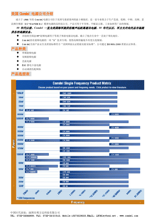
COMDEL电源中文样本
<-35dBc
220VAC,单相;
15-pin subminiature D 型
N或C
CX 1250
1250W
<-30dBc
220VAC,单相;
15-pin subminiature D 型
N或C
CX 1250A
1250W
<-30dBc
220VAC,单相;
25-pin subminiature D 型
美国 Comdel 电源公司介绍
成立于 1966 年的 Comdel 电源公司位于美国马塞诸塞州的波士顿海滨,是一家专业致力于生产直流、低频、中频、高频、甚 高频全频谱(DC- Khz-80MHz)精密电源的高科技公司。产品可用于半导体、平板显示器、工业加热等广众的领域。
80 年代以前,Comdel 一直为美国海军提供低噪声远距离通讯电源,80 年代以后,军方允许向民品市场提 供各种高频设备。
z 产品符合 ETL 和 SEMI F47 安全标准 z 标准的 RS232 串口和模拟/数字控制接口
z 前面板控制和可编程控制
可选配件
z 多种可供选择的输入交流电压工作模式
z 可外带 VCO 的频率调谐模式或内部主从工作模式 z 协议
普通技术指标
z 频率:2-30MHz 间任何一点频率 z 频率稳定度:+/-0.005% z 负载阻抗:50hms z 模拟功率要求:0-10VDC 或者 0-5VDC,代表 0 到最大输出功率 z 标准输出连接:HN,LC 或 7/16
CLF 系列可以满足应用于半导体加工的射频驱动等离子体系统的需要。应用对象包
括:刻蚀、RIE、平行板、ICP、射频溅射、CVD 和 PVD 等系统,也可用于工业系统
村田制作所 电路板插件式 (DC用) EMI静噪滤波器 (EMIFIL) 说明书
Cat.No.C31C-3关于欧盟RoHS指令·本产品目录中的所有产品都符合欧盟RoHS指令。
·欧盟RoHS指令是指欧盟的“关于在电子电气设备中限制使用某些有害物质指令2002/95/EC”。
Recycled Paper123456247135463667986本产品目录中的EMIFIL r 、EMIGUARD r 、“EMIFIL”和“EMIGUARD”是村田制作所的注册商标。
片状铁氧体磁珠开始BLM21BBLM41P阻抗值为100MHz时的代表值。
2DLM2HGDLW21SDLW5BS(AH)DLW31SNFM21CNFM21PNFM41PNFA31CNFE61P2220NFM55PNFE61PNFL21SNFW31SNFR21GNFA31GNFA21S片状EMIFIL r共模扼流线圈阻抗值为100MHz时的代表值。
开始开始3GHz频范围用45(附可变电阻器功能EMIFIL 6..............p.21–85............p.140–142BLM03BLM02BLA31BLM31BLM41BLM18BLM21BLM15BLA2ABL01BL02RN1BL02RN2BL03RN2o 片状铁氧体磁珠o 铁氧体磁珠电感器片状铁氧体磁珠铁氧体磁珠电感器" 片状铁氧体磁珠可在几MHz到几GHz频率范围内有效。
片状铁氧体磁珠作为通用静噪元件,被广泛应用于低噪声控制。
" 片状铁氧体磁珠可在低频范围内产生微小的电感。
但是在高频,电感器的电阻分量将成为主要阻抗。
当串联接入噪声产生电路中时,电感器的电阻性阻抗将阻止噪声传播。
7...............p.89–93p.97–99p.108–113.............p.144–151............p.114–116NFE31P NFE61P/HNFM21PNFM21CNFM3DCDS-6DS-9DS-9HNFA31C NFA18S806040201510C=2200pF501005001000 NFM18PNFA21So片状EMIFIL ro T型片状EMIFIL ro引线型EMIFIL r片状EMIFIL r引线型EMIFIL rT型片状EMIFIL r" 该电容器型EMI静噪滤波器对从几MHz到几百MHz的频率具有大噪声静噪效果。
FCC-EMC简介
FCC:EMC测试是针对进入欧洲的带有辐射干扰的产品所进行的测试主要有:EMI(干扰)和EMS(抗干扰)测试项目:ESD-静电抗干扰测试EFT-快速脉冲群测试SURGE-测雷击抗传导干扰掉电测试谐波电流电压闪烁传导干扰辐射干扰磁场辐射功率辐射相关测试标准就要看是哪类产品:A:家电类产品:EN55014-1,EN55014-2,EN61000-3-2,EN61000-3-3 B:IT类产品:EN55022,EN55024,EN61000-3-2,EN61000-3-3C:灯具类产品:EN55015,EN61547,EN61000-3-2,EN61000-3-3D:AV类产品:EN55013,EN55020,EN61000-3-2,EN61000-3-3至于FCC测试是美国的主要是针对无线电产品的一个认证与测试它主要是测EMI就是干扰,美国人的思想就是大家都不要干扰别人就没有干扰了这是跟EMC的区别,FCC的测试标准更简单:FCC part15和FCC part18FCC认证,又称为美国联邦通信认证,FCC(Federal Communications Commission)是美国联邦通信委员会于1934年由COMMUNICATIONACT建立是美国政府的一个独立机构,直接对国会负责。
FCC通过控制无线电广播、电视、电信、卫星和电缆来协调国内和国际的通信。
涉及美国50多个州、哥伦比亚以及美国所属地区,为确保与生命财产有关的无线电和电线通信产品的安全性,FCC的工程技术部(Office of Engineering and Technology)负责委员会的技术支持,同时负责设备认可方面的事务。
许多无线电应用产品、通讯产品和数字产品要进入美国市场,都要求FCC的认可。
联邦通讯委员会(FCC)--管理进口和使用无线电频率装置,包括电脑、传真机、电子装置、无线电接收和传输设备、无线电遥控玩具、电话、个人电脑以及其他可能伤害人身安全的产品。
Micom 2E 中文简易使用说明书
MICOM-2EALEHF-SSB Transceiver收发器BG2INPInformation for Safe,Efficient OperationExposure to Radio Frequency EnergyIn August1996,the Federal Communications Commission(FCC)adopted updated RF energy exposure guidelines for wireless products regulated by the FCC.Those guidelines are consistent with the safety standards*previously set by both U.S.and international standards bodies.The design of your Motorola two-way radio complies with the FCC guidelines and these standards.*American National Standards Institute(C95.1-1992);*National Council on Radiation Radiation Protection and Measurements(NCRP-1986);*International Commission on Non-Ionizing Radiation Protection(ICNRP-1986)To assure optimal radio performance and to insure that exposure to RF energy is within the guidelines in the above standards,properly install antennas externally on the vehicle,following recommended installation procedures.Transmit only when people inside or outside the vehicle are1to3feet away from the properly installed,externally mounted antenna;distance guidelines for the different power levels are summarized in the tablebelow:Rated power of Vehicle-Mounted Radio Distance of people from Transmitting antenna安全、高效运行信息接触射频能量1996年8月,联邦通信委员会(fcc)通过了fcc监管的无线产品射频能量暴露指南。
FCC Part 68 标准
47 CFR Ch. I (10–1–01 Edition)§65.830(i) Multiply the average lag days for interstate expenses (i.e., cash operating expenses plus interest) paid in arrears by the percentage of interstate ex-penses paid in arrears.(ii) Multiply the average lag days for interstate expenses paid in advance by the percentage of interstate expenses paid in advance. (Note: an expense lead should be shown as a negative lag.) (iii) Add the results of paragraphs (e)(2) (i) and (ii) of this section to de-termine the weighted average expense lag days.(3) Compute the weighted net lag days by deducting the weighted aver-age expense lag days from the weighted average revenue lag days.(4) Compute the percentage of a year represented by the weighted net lag days by dividing the days computed in paragraph (e)(3) of this section by 365 days.(5) Compute the cash working capital allowance by multiplying the inter-state cash operating expenses (i.e., op-erating expenses minus depreciation and amortization) plus interest by the percentage computed in paragraph(e)(4) of this section.[54 FR 9048, Mar. 3, 1989, as amended at 60 FR 12139, Mar. 6, 1995]§65.830Deducted items.(a) The following items shall be de-ducted from the interstate rate base. (1) The interstate portion of deferred taxes (Accounts 4100 and 4340).(2) The interstate portion of cus-tomer deposits (Account 4040).(3) The interstate portion of other long-term liabilities (Account4310) that were derived from the expenses speci-fied in §65.450(a).(4) The interstate portion of other de-ferred credits (Account 4360) to the ex-tent they arise from the provision of regulated telecommunications serv-ices. This shall include deferred gains related to sale-leaseback arrange-ments.(b) The interstate portion of deferred taxes, customer deposits and other de-ferred credits shall be determined as prescribed by 47 CFR part 36.(c) The interstate portion of other long-term liabilities (Account 4310) shall bear the same proportionate rela-tionships as the interstate/intrastste expenses which gave rise to the liabil-ity.[54 FR 9049, Mar. 3, 1989, as amended at 62 FR 15118, Mar. 31, 1997]PART 68—CONNECTION OF TER-M INAL EQUIPM ENT TO THE TELE-PHONE NETWORKSubpart A—GeneralSec.68.1Purpose.68.2Scope.68.3Definitions.68.4Hearing aid-compatible telephones.68.5Waivers.68.6Telephones with volume control.68.7Technical criteria for terminal equip-ment.Subpart B—Conditions on Use of TerminalEquipment68.100General.68.102Terminal equipment approval re-quirement.68.105Minimum point of entry (MPOE) anddemarcation point.68.106Notification to provider of wirelinetelecommunications.68.108Incidence of harm.68.110Compatibility of the public switchedtelephone network and terminal equip-ment.68.112Hearing aid-compatibility.68.160Designation of TelecommunicationCertification Bodies (TCBs).68.162Requirements for TelecommunicationCertification Bodies.Subpart C—Terminal Equipment ApprovalProcedures68.201Connection to the public switchedtelephone network.68.211Terminal equipment approval revoca-tion procedures.68.213Installation of other than ‘‘fully pro-tected’’ non-system simple customer premises wiring.68.214Changes in other than ‘‘fully pro-tected’’ premises wiring that serves fewer than four subscriber access lines. 68.215Installation of other than ‘‘fully-pro-tected’’ system premises wiring that serves more than four subscriber access lines.68.218Responsibility of the party acquiringequipment authorization.68.224Notice of non-hearing aid compat-ibility.Federal Communications Commission§68.2Subpart D—Conditions for TerminalEquipment Approval68.300Labeling requirements.68.316Hearing aid compatibility: Technicalrequirements.68.317Hearing aid compatibility volumecontrol: technical standards.68.318Additional limitations.68.320Supplier’s Declaration of Conformity.68.321Location of responsible party.68.322Changes in name, address, ownershipor control of responsible party.68.324Supplier’s Declaration of Conformityrequirements.68.326Retention of records.68.346Description of testing facilities.68.348Changes in equipment and circuitrysubject to a Supplier’s Declaration of Conformity.68.350Revocation of Supplier’s Declarationof Conformity.68.354Numbering and labeling requirementsfor terminal equipment.Subpart E—Complaint Procedures68.400Content.68.402Amended complaints.68.404Number of copies.68.406Service.68.408Answers to complaints and amendedcomplaints.68.410Replies to answers or amended an-swers.68.412Defective pleadings.68.414Hearing aid-compatibility: E nforce-ment.68.415Hearing aid-compatibility and vol-ume control informal complaints.68.417Informal complaints; form and con-tent.68.418Procedure; designation of agents forservice.68.419Answers to informal complaints.68.420Review and disposition of informalcomplaints.68.423Actions by the Commission on itsown motion.Subpart F[Reserved]Subpart G—Administrative Council forTerminal Attachments68.602Sponsor of the Administrative Coun-cil for Terminal Attachments.68.604Requirements for submitting tech-nical criteria.68.608Publication of technical criteria.68.610Database of terminal equipment.68.612Labels on terminal equipment.68.614Oppositions and appeals.A UTHORITY: 47 U.S.C. 154, 303.Subpart A—GeneralA UTHORITY: Secs. 4, 5, 303, 48 Stat., as amended, 1066, 1068, 1082; (47 U.S.C. 154, 155, 303).S OURCE: 45 FR 20841, Mar. 31, 1980, unless otherwise noted.§68.1Purpose.The purpose of the rules and regula-tions in this part is to provide for uni-form standards for the protection of the telephone network from harms caused by the connection of terminal equipment and associated wiring there-to, and for the compatibility of hearing aids and telephones so as to ensure that persons with hearing aids have reasonable access to the telephone net-work.(47 U.S.C. 151, 154(i), 154(j), 201–205, 218, 220, 313, 403, 412, and 5 U.S.C. 553)[49 FR 21733, May 23, 1984]§68.2Scope.(a) E xcept as provided in paragraphs(b) and (c) of this section, the rules and regulations apply to direct connection of all terminal equipment to the public switched telephone network for use in conjunction with all services other than party line services.(b) National defense and security. Where the Secretary of Defense or au-thorized agent or the head of any other governmental department, agency, or administration (approved in writing by the Commission to act pursuant to this rule) or authorized representative, cer-tifies in writing to the appropriate common carrier that compliance with the provisions of part 68 could result in the disclosure of communications equipment or security devices, loca-tions, uses, personnel, or activity which would adversely affect the na-tional defense and security, such equip-ment or security devices may be con-nected to the telephone company pro-vided communications network with-out compliance with this part, provided that each written certification states that:(1) The connection is required in the interest of national defense and secu-rity;(2) The equipment or device to be connected either complies with the47 CFR Ch. I (10–1–01 Edition)§68.3technical criteria pertaining thereto or will not cause harm to the nationwide telephone network or to employees of any provider of wireline telecommuni-cations; and(3) The installation is performed by well-trained, qualified employees under the responsible supervision and control of a person who is a licensed profes-sional engineer in the jurisdiction in which the installation is performed. (c) Governmental departments, agen-cies, or administrations that wish to qualify for interconnection of equip-ment or security devices pursuant to this section shall file a request with the Secretary of this Commission stat-ing the reasons why the exemption is requested. A list of these departments, agencies, or administrations that have filed requests shall be published in the F EDERAL R EGISTER. The Commission may take action with respect to those requests 30 days after publication. The Commission action shall be published in the F EDERAL R EGISTER. However, the Commission may grant, on less than the normal notice period or without notice, special temporary authority, not to exceed 90 days, for governmental departments, agencies, or administra-tions that wish to qualify for inter-connection of equipment or security devices pursuant to this section. Re-quests for such authority shall state the particular fact and circumstances why authority should be granted on less than the normal notice period or without notice. In such cases, the Com-mission shall endeavor to publish its disposition as promptly as possible in the F EDERAL R EGISTER.[66 FR 7580, Jan. 24, 2001]§68.3Definitions.As used in this part:Demarcation point (also point of inter-connection). As used in this part, the point of demarcation and/or inter-connection between the communica-tions facilities of a provider of wireline telecommunications, and terminal equipment, protective apparatus or wiring at a subscriber’s premises. Essential telephones. Only coin-oper-ated telephones, telephones provided for emergency use, and other tele-phones frequently needed for use by persons using such hearing aids.Harm. E lectrical hazards to the per-sonnel of providers of wireline tele-communications, damage to the equip-ment of providers of wireline tele-communications, malfunction of the billing equipment of providers of wireline telecommunications, and deg-radation of service to persons other than the user of the subject terminal equipment, his calling or called party. Hearing aid compatible. Except as used at §§68.4(a)(3) and 68.414, the terms hearing aid compatible or hearing aid compatibility are used as defined in §68.316, unless it is specifically stated that hearing aid compatibility volume control, as defined in §68.317, is in-tended or is included in the definition. Inside wiring or premises wiring. Cus-tomer-owned or controlled wire on the subscriber’s side of the demarcation point.Premises. As used herein, generally a dwelling unit, other building or a legal unit of real property such as a lot on which a dwelling unit is located, as de-termined by the provider of tele-communications service’s reasonable and nondiscriminatory standard oper-ating practices.Private radio services. Private land mobile radio services and other com-munications services characterized by the Commission in its rules as private radio services.Public mobile services. Air-to-ground radiotelephone services, cellular radio telecommunications services, offshore radio, rural radio service, public land mobile telephone service, and other common carrier radio communications services covered by part 22 of Title 47 of the Code of Federal Regulations. Responsible party. The party or par-ties responsible for the compliance of terminal equipment or protective cir-cuitry intended for connection directly to the public switched telephone net-work with the applicable rules and reg-ulations in this part and with the tech-nical criteria published by the Admin-istrative Council for Terminal Attach-ments. If a Telecommunications Cer-tification Body certifies the terminal equipment, the responsible party is the holder of the certificate for that equip-ment. If the terminal equipment is the subject of a Supplier’s Declaration of Conformity, the responsible party shallFederal Communications Commission§68.5be: the manufacturer of the terminal equipment, or the manufacturer of pro-tective circuitry that is marketed for use with terminal equipment that is not to be connected directly to the net-work, or if the equipment is imported, the importer, or if the terminal equip-ment is assembled from individual component parts, the assembler. If the equipment is modified by any party not working under the authority of the re-sponsible party, the party performing the modifications, if located within the U.S., or the importer, if the equipment is imported subsequent to the modi-fications, becomes the new responsible party. Retailers or original equipment manufacturers may enter into an agreement with the assembler or im-porter to assume the responsibilities to ensure compliance of the terminal equipment and to become the respon-sible party.Secure telephones. Telephones that are approved by the United States Govern-ment for the transmission of classified or sensitive voice communications. Terminal equipment. As used in this part, communications equipment lo-cated on customer premises at the end of a communications link, used to per-mit the stations involved to accom-plish the provision of telecommuni-cations or information services.[66 FR 7581, Jan. 24, 2001]§68.4Hearing aid-compatible tele-phones.(a)(1) Except for telephones used with public mobile services, telephones used with private radio services, and cordless and secure telephones, every telephone manufactured in the United States (other than for export) or im-ported for use in the United States after August 16, 1989, must be hearing aid compatible, as defined in §68.316. Every cordless telephone manufactured in the United States (other than for ex-port) or imported into the United States after August 16, 1991, must be hearing aid compatible, as defined in §68.316.(2) Unless otherwise stated and ex-cept for telephones used with public mobile services, telephones used with private radio services and secure tele-phones, every telephone listed in §68.112 must be hearing aid compatible, as defined in §68.316.(3) A telephone is hearing aid-com-patible if it provides internal means for effective use with hearing aids that are designed to be compatible with tele-phones which meet established tech-nical standards for hearing aid compat-ibility.(4) The Commission shall revoke or otherwise limit the exemptions of paragraph (a)((1) of this section for telephones used with public mobile services or telephones used with pri-vate radio services if it determines that (i) such revocation or limitation is in the public interest; (ii) continuation of the exemption without such revoca-tion or limitation would have an ad-verse effect on hearing-impaired indi-viduals; (iii) compliance with the re-quirements of §68.4(a)(1) is techno-logically feasible for the telephones to which the exemption applies; and (iv) compliance with the requirements of §68.4(a)(1) would not increase costs to such an extent that the telephones to which the exemption applies could not be successfully marketed.[54 FR 21430, May 18, 1989, as amended at 55 FR 28763, July 13, 1990; 57 FR 27183, June 18, 1992; 61 FR 42186, Aug. 14, 1996]§68.5Waivers.The Commission may, upon the ap-plication of any interested person, ini-tiate a proceeding to waive the require-ments of §68.4(a)(1) with respect to new telephones, or telephones associated with a new technology or service. The Commission shall not grant such a waiver unless it determines, on the basis of evidence in the record of such proceeding, that such telephones, or such technology or service, are in the public interest, and that (a) compli-ance with the requirements of §68.4(a)(1) is technologically infeasible, or (b) compliance with such require-ments would increase the costs of the telephones, or of the technology or service, to such an extent that such telephones, technology, or service could not be successfully marketed. In any proceeding under this section to grant a waiver from the requirements of §68.4(a)(1), the Commission shall consider the effect on hearing-impaired individuals of granting the waiver. The47 CFR Ch. I (10–1–01 Edition)§68.6Commission shall periodically review and determine the continuing need for any waiver granted pursuant to this section.[54 FR 21430, May 18, 1989]§68.6Telephones with volume control. As of January 1, 2000, all telephones, including cordless telephones, as de-fined in §15.3(j) of this chapter, manu-factured in the United States (other than for export) or imported for use in the United States, must have volume control in accordance with §68.317. Se-cure telephones, as defined by §68.3 are exempt from this section, as are tele-phones used with public mobile serv-ices or private radio services.[62 FR 43484, Aug. 14, 1997]§68.7Technical criteria for terminal equipment.(a) Terminal equipment shall not cause harm, as defined in §68.3, to the public switched telephone network. (b) Technical criteria published by the Administrative Council for Ter-minal Attachments are the presump-tively valid technical criteria for the protection of the public switched tele-phone network from harms caused by the connection of terminal equipment, subject to the appeal procedures in §68.614 of this part.[66 FR 7581, Jan. 24, 2001]Subpart B—Conditions on Use ofTerminal Equipment§68.100General.In accordance with the rules and reg-ulations in this part, terminal equip-ment may be directly connected to the public switched telephone network, in-cluding private line services provided over wireline facilities that are owned by providers of wireline telecommuni-cations.[66 FR 7581, Jan. 24, 2001]§68.102Terminal equipment approval requirement.Terminal equipment must be ap-proved in accordance with the rules and regulations in subpart C of this part, or connected through protective circuitry that is approved in accord-ance with the rules and regulations in subpart C.[66 FR 7582, Jan. 24, 2001]§68.105Minimum point of entry (MPOE) and demarcation point. (a) Facilities at the demarcation point. Carrier-installed facilities at, or con-stituting, the demarcation point shall consist of wire or a jack conforming to the technical criteria published by the Administrative Council for Terminal Attachments.(b) Minimum point of entry. The ‘‘min-imum point of entry’’ (MPOE) as used herein shall be either the closest prac-ticable point to where the wiring crosses a property line or the closest practicable point to where the wiring enters a multiunit building or build-ings. The reasonable and nondiscrim-inatory standard operating practices of the provider of wireline telecommuni-cations services shall determine which shall apply. The provider of wireline telecommunications services is not precluded from establishing reasonable classifications of multiunit premises for purposes of determining which shall apply. Multiunit premises include, but are not limited to, residential, com-mercial, shopping center and campus situations.(c) Single unit installations. For single unit installations existing as of August 13, 1990, and installations installed after that date the demarcation point shall be a point within 30 cm (12 in) of the protector or, where there is no pro-tector, within 30 cm (12 in) of where the telephone wire enters the customer’s premises, or as close thereto as prac-ticable.(d) Multiunit installations. (1) In mul-tiunit premises existing as of August 13, 1990, the demarcation point shall be determined in accordance with the local carrier’s reasonable and non-dis-criminatory standard operating prac-tices. Provided, however, that where there are multiple demarcation points within the multiunit premises, a de-marcation point for a customer shall not be further inside the customer’s premises than a point twelve inches from where the wiring enters the cus-tomer’s premises, or as close thereto as practicable.Federal Communications Commission§68.106(2) In multiunit premises in which wiring is installed, including major ad-ditions or rearrangements of wiring ex-isting prior to that date, the provider of wireline telecommunications may place the demarcation point at the minimum point of entry (MPOE). If the provider of wireline telecommuni-cations services does not elect to estab-lish a practice of placing the demarca-tion point at the minimum point of entry, the multiunit premises owner shall determine the location of the de-marcation point or points. The multi-unit premises owner shall determine whether there shall be a single demar-cation point location for all customers or separate such locations for each cus-tomer. Provided, however, that where there are multiple demarcation points within the multiunit premises, a de-marcation point for a customer shall not be further inside the customer’s premises than a point 30 cm (12 in) from where the wiring enters the cus-tomer’s premises, or as close thereto as practicable. At the time of installa-tion, the provider of wireline tele-communications services shall fully in-form the premises owner of its options and rights regarding the placement of the demarcation point or points and shall not attempt to unduly influence that decision for the purpose of ob-structing competitive entry.(3) In any multiunit premises where the demarcation point is not already at the MPOE, the provider of wireline telecommunications services must comply with a request from the prem-ises owner to relocate the demarcation point to the MPOE. The provider of wireline telecommunications services must negotiate terms in good faith and complete the relocation within forty-five days from said request. Premises owners may file complaints with the Commission for resolution of allega-tions of bad faith bargaining by pro-vider of wireline telecommunications services. See 47 U.S.C. 208; 47 CFR 1.720 through 1.736 (1999).(4) The provider of wireline tele-communications services shall make available information on the location of the demarcation point within ten business days of a request from the premises owner. If the provider of wireline telecommunications services does not provide the information with-in that time, the premises owner may presume the demarcation point to be at the MPOE. Notwithstanding the provi-sions of §68.110(c) of this part, provider of wireline telecommunications serv-ices must make this information freely available to the requesting premises owner.(5) In multiunit premises with more than one customer, the premises owner may adopt a policy restricting a cus-tomer’s access to wiring on the prem-ises to only that wiring located in the customer’s individual unit that serves only that particular customer.[66 FR 7582, Jan. 24, 2001]§68.106Notification to provider of wireline telecommunications.(a) General. Customers connecting terminal equipment or protective cir-cuitry to the public switched telephone network shall, upon request of the pro-vider of wireline telecommunications, inform the provider of wireline tele-communications of the particular line(s) to which such connection is made, and any other information re-quired to be placed on the terminal equipment pursuant to §68.354 of this part by the Administrative Council for Terminal Attachments.(b) Systems assembled of combinations of individually-approved terminal equip-ment and protective circuitry. Customers connecting such assemblages to the public switched telephone network shall, upon the request of the provider of wireline telecommunications, pro-vide to the provider of wireline tele-communications the following infor-mation:For each line:(1) Information required for compat-ible operation of the equipment with the communications facilities of the provider of wireline telecommuni-cations;(2) The identifying information re-quired to be placed on terminal equip-ment pursuant to §68.354 for all equip-ment dedicated to that line; and(3) Any other information regarding equipment dedicated to that line re-quired to be placed on the terminal equipment by the Administrative Council for Terminal Attachments.47 CFR Ch. I (10–1–01 Edition)§68.108(4) A list of identifying numbers re-quired to be placed on terminal equip-ment, if any, by the Administrative Council for Terminal Attachments, pursuant to §68.354 of this part, for equipment to be used in the system. (c) Systems using other than ‘‘fully pro-tected’’ premises wiring. Customers who intend to connect premises wiring other than ‘‘fully protected’’ premises wiring to the public switched telephone network shall, in addition to the fore-going, give notice to the provider of wireline telecommunications in ac-cordance with §68.215(e).[66 FR 7582, Jan. 24, 2001]§68.108Incidence of harm.Should terminal equipment, inside wiring, plugs and jacks, or protective circuitry cause harm to the public switched telephone network, or should the provider of wireline telecommuni-cations reasonably determine that such harm is imminent, the provider of wireline telecommunications shall, where practicable, notify the customer that temporary discontinuance of serv-ice may be required; however, wherever prior notice is not practicable, the pro-vider of wireline telecommunications may temporarily discontinue service forthwith, if such action is reasonable under the circumstances. In case of such temporary discontinuance, the provider of wireline telecommuni-cations shall:(a) Promptly notify the customer of such temporary discontinuance;(b) Afford the customer the oppor-tunity to correct the situation which gave rise to the temporary discontinu-ance; and(c) Inform the customer of his right to bring a complaint to the Commis-sion pursuant to the procedures set forth in subpart E of this part.[55 FR 28630, July 12, 1990, as amended at 66 FR 7583, Jan. 24, 2001]§68.110Compatibility of the public switched telephone network and terminal equipment.(a) Availability of interface information. Technical information concerning interface parameters not specified by the technical criteria published by the Administrative Council for Terminal Attachments, that are needed to per-mit terminal equipment to operate in a manner compatible with the commu-nications facilities of a provider of wireline telecommunications, shall be provided by the provider of wireline telecommunications upon request. (b) Changes in the facilities, equipment, operations, or procedures of a provider of wireline telecommunications. A provider of wireline telecommunications may make changes in its communications facilities, equipment, operations or procedures, where such action is rea-sonably required in the operation of its business and is not inconsistent with the rules and regulations in this part. If such changes can be reasonably ex-pected to render any customer’s ter-minal equipment incompatible with the communications facilities of the provider of wireline telecommuni-cations, or require modification or al-teration of such terminal equipment, or otherwise materially affect its use or performance, the customer shall be given adequate notice in writing, to allow the customer an opportunity to maintain uninterrupted service.(c) Availability of inside wiring infor-mation. Any available technical infor-mation concerning wiring on the cus-tomer side of the demarcation point, including copies of existing schematic diagrams and service records, shall be provided by the provider of wireline telecommunications upon request of the building owner or agent thereof. The provider of wireline telecommuni-cations may charge the building owner a reasonable fee for this service, which shall not exceed the cost involved in lo-cating and copying the documents. In the alternative, the provider of wireline telecommunications may make these documents available for re-view and copying by the building owner. In this case, the provider of wireline telecommunications may charge a reasonable fee, which shall not exceed the cost involved in making the documents available, and may also require the building owner to pay a de-posit to guarantee the documents’ re-turn.[66 FR 7583, Jan. 24, 2001]。
EMI EMC设计秘籍

微波暗室、宽频天线、EMI专用频谱仪、LISN、EMI软件集成 --------------------------------------------------------------------------------------------------------------------------------------------------------------全球首创的EMI集成测试系统放射性干扰噪声测试EMI/EMC设计秘籍——电子产品设计工程师必备手册微波暗室、宽频天线、EMI专用频谱仪、LISN、EMI软件集成 --------------------------------------------------------------------------------------------------------------------------------------------------------------全球首创的EMI集成测试系统放射性干扰噪声测试目 录一、EMC工程师必须具备的八大技能二、EMC常用元件三、EMI/EMC设计经典85问四、EMC专用名词大全五、产品内部的EMC设计技巧六、电磁干扰的屏蔽方法七、电磁兼容(EMC)设计如何融入产品研发流程微波暗室、宽频天线、EMI专用频谱仪、LISN、EMI软件集成 --------------------------------------------------------------------------------------------------------------------------------------------------------------全球首创的EMI 集成测试系统 放射性干扰噪声测试一、EMC工程师必须具备的八大技能EMC工程师需要具备那些技能?从企业产品需要进行设计、整改认证的过程看,EMC工程师必须具备以下八大技能:1、EMC的基本测试项目以及测试过程掌握;2、产品对应EMC的标准掌握;3、产品的EMC整改定位思路掌握;4、产品的各种认证流程掌握;5、产品的硬件硬件知识,对电路(主控、接口)了解;6、EMC设计整改元器件(电容、磁珠、滤波器、电感、瞬态抑制器件等)使用掌握;7、产品结构屏蔽设计技能掌握;8、对EMC设计如何介入产品各个研发阶段流程掌握。
村田EMI滤波器规格书

Cat.No.C31C-4关于欧盟RoHS指令・本产品目录中的所有产品都符合欧盟RoHS指令。
・欧盟RoHS指令是指欧盟的“关于在电子电气设备中限制使用某些有害物质指令2002/95/EC”。
・详情请参见本公司网站“Murata's Approach for EU RoHS”(/info/rohs.html)。
12345624713646769818592目录本产品目录中的EMIFIL r 、EMIGUARD r 、“EMIFIL”和“EMIGUARD”是村田制作所的注册商标。
EMI静噪滤波器选择指南片状铁氧体磁珠开始BLM41P阻抗值为100MHz时的代表值。
2DLW5BS(AH)DLW31SNFM41PNFA31C2220NFM55PNFE61PNFL21SNFA31GNFA21S开始开始片状EMIFIL r共模扼流线圈3EMI静噪滤波器选择指南品种一览表/有效频率范围4品种一览表/有效频率范围5品种一览表/有效频率范围6..............p.21–91............p.146–148BLM03BLM02BLA31BLM31BLM41BLM18BLM21BLM15BLA2ABL01BL02RN1BL02RN2BL03RN2片状铁氧体磁珠铁氧体磁珠电感器o 片状铁氧体磁珠o 铁氧体磁珠电感器" 片状铁氧体磁珠可在几MHz到几GHz频率范围内有效。
片状铁氧体磁珠作为通用静噪元件,被广泛应用于低噪声控制。
" 片状铁氧体磁珠可在低频范围内产生微小的电感。
但是在高频,电感器的电阻分量将成为主要阻抗。
当串联接入噪声产生电路中时,电感器的电阻性阻抗将阻止噪声传播。
DC用EMI静噪滤波器 (EMIFIL r ) 概要介绍7...............p.95–99p.103–105p.114–120.............p.150–158............p.121–122NFE31P NFE61P/HNFM21P NFM31PNFM21CNFM3DCDS-6DS-9DS-9HNFA31C NFA18S806040201510C=2200pF501005001000 NFM18PNFA21S片状EMIFIL r引线型EMIFIL rT型片状EMIFIL ro片状EMIFIL ro T型片状EMIFIL ro引线型EMIFIL r" 该电容器型EMI静噪滤波器对从几MHz到几百MHz的频率具有大噪声静噪效果。
EMI电源滤波器基本知识介绍
EMI电源滤波器基本知识介绍电磁干扰:因电磁骚扰引起设备、装置或系统性能下降的都是电磁干扰。
随着电子技术的迅速发展,电子设备得到广泛的应用,电磁环境污染日趋严重,已成为当今主要公害之一,越来越引起世界各国各行各业的广泛关注。
在许多领域,电磁兼容性已成为电气和电子产品必须有的技术指标或性能评价的依据,甚至关系到一个企业或一种产品的生死存亡。
EMI电源滤波器:电磁干扰(EMI)电源滤波器(以下简称滤波器)是由电感、电容等构成的无源双向多端口网络。
实际上它起两个低通滤波器的作用,一个衰减共模干扰,另一个衰减差模干扰。
它能在阻带(通常大于10KHz)范围内衰减射频能量而让工频无衰减或很少衰减地通过。
EMI电源滤波器是电子设备设计工程师控制传导电磁干扰和辐射电磁干扰的首选工具。
插入损耗:滤波器的插入损耗是不用滤波器时从噪声源传递到负载的噪声电压与插入滤波器时负载上的噪声电压之比。
插入损耗是在空载、50Ω系统条件下测试的,结果通常表示为在所关心频段内的衰减曲线(单位为分贝)。
插入损耗的计算可由下式求得:式中:V1 ─没有滤波器时负载上的噪声电压;V2 ─插入滤波器时负载上的噪声电压。
滤波器插入损耗测量结果通常表示为两种形式:一是插入损耗对频率的曲线,二是数据表。
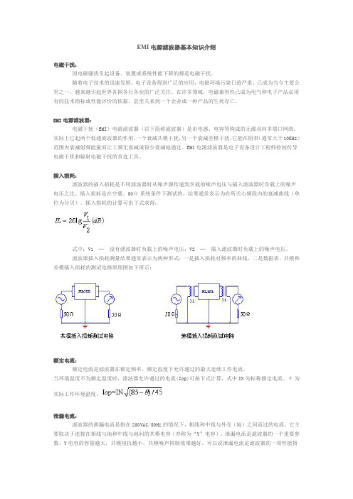
共模和差模插入损耗的测试电路原理图如下所示:额定电流:额定电流是滤波器在额定频率、额定温度下允许通过的最大连续工作电流。
当环境温度不为额定温度时,滤波器允许通过的电流(Iop)可按下式计算,式中IN为标称额定电流、θ为实际工作环境温度,泄漏电流:滤波器的泄漏电流是指在250VAC/50Hz的情况下,相线和中线与外壳(地)之间流过的电流。
它主要取决于连接在相线与地和中线与地间的共模电容(亦称为“Y”电容)。
泄漏电流是滤波器的一个重要参数。
Y电容的容量越大,共模阻抗越小,共模噪声抑制效果越好。
可以说泄漏电流是滤波器的一项性能指标, 泄漏电流越大,滤波器性能越好。
zif-67的电导率
zif-67的电导率
ZIF-67(Co)是一种金属有机框架(MOF)材料,由钴离子(Co2+)和2-甲基咪唑酸根(Hmim)组成,具有立方晶系的结构,单胞参数为16.9589 Å,是典型的多孔材料。
ZIF-67(Co)的孔径、比表面积和孔容等参数可以通过调节其合成条件进行控制。
关于ZIF-67的电导率,现有文献表明其具有较高的电导率。
这主要归功于其具有高度可调的孔径、比表面积和多孔性质。
ZIF-67的高比表面积使其能够提供更多的活性位点,从而提高电导率。
此外,ZIF-67的孔径和孔容也可以通过调节其合成条件进行优化,进一步改善其电导率性能。
然而,对于ZIF-67的具体电导率数值,不同文献报道的结果可能存在差异。
这可能是由于合成条件、实验方法等因素的影响。
因此,为了获得更准确和可靠的电导率数据,建议查阅最新的研究文献或权威的科技报告。
总之,ZIF-67是一种具有优异电导率的金属有机框架材料。
其高比表面积、可调的孔径和多孔性质使其在电化学领域具有广泛的应用前景。
通过进一步优化合成条件和实验方法,可以进一步改善ZIF-67的电导率性能,为其在电化学领域的应用提供更好的基础。
RF电磁干扰EMI滤波器和滤波连接器的基本概述

环测威官网:/电磁干扰(EMI)领域最初在1933年由巴黎国际电工委员会(IEC)的一个小组委员会悄然获得了正式认可。
在CISPR(国际无线电干扰特别委员会)的名义下,成立小组委员会是为了更好地了解射频技术可能产生的长期复杂情况。
自1820年莫尔斯,亨利和韦尔成立以来,无线电的受欢迎程度已经爆发,成为大萧条时期必不可少的家用电器。
很快就确定有意和无意的RF传输开始影响其他电气系统,从而导致电子界对EMI的认识不断提高。
1934年在整个20世纪60年代,70年代和80年代,研究人员越来越担心电磁辐射的干扰增加。
1967年,美国军方颁布了Mil Standard 461A,该标准为已经在军事应用中使用的电子设备以及新军用电子设备的排放和易感性限制建立了测试和验证要求。
1979年,美国联邦通信委员会(FCC)对美国所有数字设备的电磁辐射实施法律限制。
随着系统变得更快,更小,更强大,随着新兴技术的出现,这些法规不断发展。
更倾向于干扰其他电气系统的运行。
为了更好地了解噪声是如何产生的,航空电子设备和航空航天工程师已经研究了与EMI 相关的问题,并确定了可以设计新系统以最大限度地降低传输噪声的方法,同时还能够承受来自外部源的一定量噪声。
最初,大多数公司选择了快速,笨重的屏蔽外壳设计,这些设计仅仅是最低效的法拉第笼。
来自寻求更好的长期解决方案以消除其敏感电子设备中EMI敏感性的公司的更精明的研究人员倾向于采用更专业,更专注的方法,结合更好的电子设计和布局,同时在需要时加入额外的屏蔽和滤波元件。
环测威官网:/创建多个认证级别有助于确保电气系统在辐射和传导发射和易感性方面的兼容性。
这些标准的引入使专业人员能够轻松识别可以集成到自己的组件中的电气系统,而无需担心EMI问题。
今天,由于这些更严格的法规不断融入不断扩大的电子领域,所有类型的设备,尤其是高度敏感的侦察,医疗和航空电子设备,都比“嘈杂”EMI造成灾难性故障的风险更安全。
Micrel MIC2778 电压监测器说明书
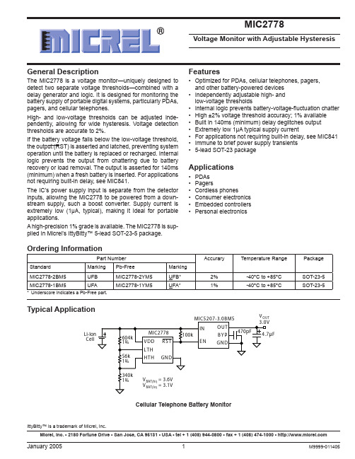
Voltage Monitor with Adjustable HysteresisGeneral Description The MIC2778 is a voltage monitor—uniquely designed to detect two separate voltage thresholds—combined with a delay generator and logic. It is designed for monitoring the battery supply of portable digital systems, particularly PDAs, pagers, and cellular telephones.High- and low-voltage thresholds can be adjusted inde-pendently, allowing for wide hysteresis. Voltage detection thresholds are accurate to 2%.If the battery voltage falls below the low-voltage threshold, the output (RST) is asserted and latched, preventing system operation until the battery is replaced or recharged. Internal logic prevents the output from chattering due to battery recovery or load removal. The output is asserted for 140ms (minimum) when a fresh battery is inserted. For applications not requiring built-in delay, see MIC841.The IC’s power supply input is separate from the detector inputs, allowing the MIC2778 to be powered from a down-stream supply, such a boost converter. Supply current is extremely low (1µA, typical), making it ideal for portable applications.A high-precision 1% grade is available. The MIC2778 is sup-plied in Micrel’s IttyBitty™ 5-lead SOT-23-5 package.Typical ApplicationLi-Ion CellV OUT Cellular Telephone Battery MonitorFeatures• Optimized for PDAs, cellular telephones, pagers, and other battery-powered devices • Independently adjustable high- and low-voltage thresholds• Internal logic prevents battery-voltage-fluctuation chatter • High ±2% voltage threshold accuracy; 1% available • Built in 140ms (minimum) delay deglitches output• Extremely low 1µA typical supply current• For applications not requiring built-in delay, see MIC841• Immune to brief power supply transients • 5-lead SOT-23 packageApplications• PDAs • Pagers• Cordless phones• Consumer electronics • Embedded controllers •Personal electronicsMicrel, Inc. • 2180 Fortune Drive • San Jose, CA 95131 • USA • tel + 1 (408) 944-0800 • fax + 1 (408) 474-1000 • IttyBitty™ is a trademark of Micrel, Inc.Ordering InformationPart NumberAccuraryTemperature RangePackageStandard Marking Pb-Free Marking MIC2778-2BM5UFB MIC2778-2YM5UFB*2%-40°C to +85°C SOT-23-5MIC2778-1BM5UFAMIC2778-1YM5UFA*1%-40°C to +85°CSOT-23-5* Underscore indicates a Pb-Free part.Pin DescriptionPin NumberPin Name Pin Function1HTHHigh-Voltage Theshold (Input): Analog input to a comparator. When the level on this pin initially rises above V REF , the delay generator cycles and the RST remains low for a minimum of 140ms.2 GND Ground3LTHLow-Voltage Threshold (Input): Analog input to a comparator. This is the voltage monitor input assigned to detect a low voltage condition. When the level on this pin falls below V REF , RST is asserted and the condition is latched until V HTH > V REF .4 RSTReset (Output): Active-low, open-drain output. This output is asserted and latched when V LTH <V REF , indicating a low voltage condition. This state remains latched until V HTH > V REF .5 VDDPower Supply (Input): Independent supply input for internal circuitry.Pin ConfigurationHTHLTH GND SOT-23-5 (M5)Absolute Maximum Ratings (Note 1)Supply Voltage (V DD ) .......................................–0.3V to +7V Input Voltages (V HI , V LO ) .................................–0.3V to +7V RST Output Current (I RST ) .........................................20mA Storage Temperature (T S ) ........................–65°C to +150°C ESD Rating, Note 3 .......................................................2kVOperating Ratings (Note 2)Supply Voltage (V DD ) ..................................+1.5V to +5.5VInput Voltages (V RST , V LTH , V HTH ) ................–0.3V to +6.0V Ambient Temperature Range (T A ) ..............–40°C to +85°C Package Thermal Resistance ................................256°C/WElectrical Characteristics1.5V ≤ V DD ≤ 5.5V; T A = +25°C, bold values indicate –40°C ≤ T A ≤ +85°C; unless noted Symbol Parameter Condition Min Typ Max Units I DD Supply Current RST not asserted 1 2 µA I LTH, I HTH Input Leakage Current5pA10 nA V REF Reference Voltage1.240 V MIC2778-2 1.215 1.265 VMIC2778-11.228 1.252 V t DPropagation Delay V LTH = V REF(max) +100mV to 5 µsV REF(min) – 100mV t RESET Reset Pulse Width140 420 ms V RST Voltage-Low Reset RST asserted, I SINK = 1.6mA, V DD ≥ 1.6V 0.3 VRST asserted, I SINK = 100µA, V DD ≥ 1.2V,0.4VNote 1. Exceeding the absolute maximum rating may damage the device.Note 2. The device is not guaranteed to function outside its operating rating.Note 3. Devices are ESD sensitive. Handling precautions recommended. Human body model, 1.5k in series with 100pF.Note 4. V DD operating range is 1.5V to 5.5V. Output is guaranteed to be held low down to V DD = 1.2V.Timing DiagramV BATTV RST Propagation delays not shown for clarity.Note A. The MIC2778 ignores very brief transients.See “Applications Information” for details.Functional DescriptionThe MIC2778 monitors the voltage of a battery and detects when it is discharged below a programmed level. Upon be-ing replaced, or being recharged above a second higher programmed trip point, the output remains low for a minimum of 140ms and then sends a reset signal to a microprocessor or other downstream component.Voltage Low OutputThe voltage-low output (RST) is an active-low, open-drain output which sinks current when the MIC2778 detects a low input voltage.Functional DiagramR S TV V Trip PointsBattery voltage is monitored by a comparator via a voltage divider network. The divided voltage is compared to an in-ternal reference voltage. When the voltage at the LTH input pin drops below the internal reference voltage, the output pulls low. At this point, the voltage at HTH is assumed to be below the reference voltage.DelayAt power-on or when the battery is replaced or recharged, and the voltage at HTH exceeds the reference voltage, the output goes high after a minimum delay of 140ms.Applications InformationOutputSince the MIC2778 output is an open-drain MOSFET, most applications will require a pull-up resistor. The value of the resistor should not be too large or leakage effects may domi-nate. 470kΩ is the maximum recommended value.Programming the ThresholdsThe low-voltage threshold is calculated using:V V R1R2R3R2R3BAT(lo)REF =+++The high-voltage threshold is calculated using:V V R1R2R3R3BAT(hi)REF =++where, for both equations:V 1.240V REF =In order to provide the additional criteria needed to solve for the resistor values, the resistors can be selected such that they have a given total value, that is, R1 + R2 + R3 = R TOTAL . A value such as 1MΩ for R TOTAL is a reasonable value because it draws minimum battery current but has no significant effect on accuracy.When working with large resistors, a small amount of leak-age current can cause voltage offsets that degrade system accuracy. The maximum recommended total resistance from V BAT to ground is 3MΩ.Figure 1. Example CircuitOnce the desired trip points are determined, set the V BAT(hi) threshold first.For example, use a total of 1MΩ = R1 + R2 + R3. For a typical single-cell lithium ion battery, 3.6V is a good “high threshold” because at 3.6V the battery is moderately charged. Solving for R3:V 1.241M R3BAT(hi)=ΩR3344k =ΩOnce R3 is determined, the equation for V BAT(lo) can be used to determine R2. A single lithium-ion cell should not be discharged below 2.5V. Many applications limit the drain to 3.1V. Using 3.1V for the V BAT(lo) threshold allows calculationof the two remaining resistor values.V 3.1V 1.241M R2344k BAT(lo)==Ω+R256k =ΩR11M R2R3=−−ΩR1600k =ΩThe accuracy of the resistors can be chosen based upon the accuracy required by the system.Input TransientsThe MIC2778 is inherently immune to very short negative-going “glitches.” Very brief transients may exceed the V BAT(lo) threshold without tripping the output.As shown in Figure 2, the narrower the transient, the deeper the threshold overdrive that will be ignored by the MIC2778. The graph represents the typical allowable transient dura-tion for a given amount of threshold overdrive that will not generate a reset.20406080100120140M A X . T R A N S I E N T D U R A T I O N (µs )RESET COMP. OVERDRIVE,V REF –V LTH (mV)Input Trans ient Figure 2. Input Transient ResponseInterfacing to Processors With Bidirectional Reset PinsSome microprocessors have reset signal pins that are bidi-rectional, rather than input only. The Motorola 68HC11 family is one example. Because the MIC2778’s output is open drain, it can be connected directly to the processor’s reset pin using only the pull-up resistor normally required. See Figure 3.Figure 3. Interfacing to Bidirectional Reset PinPackage InformationSOT-23-5 (M5)MICREL INC. 2180 FORTUNE DRIVE SAN JOSE, CA 95131 USATEL + 1 (408) 944-0800 FAX + 1 (408) 474-1000 WEB This information furnished by Micrel in this data sheet is believed to be accurate and reliable. However no responsibility is assumed by Micrel for its use.Micrel reserves the right to change circuitry and specifications at any time without notification to the customer.Micrel Products are not designed or authorized for use as components in life support appliances, devices or systems where malfunction of a product can reasonably be expected to result in personal injury. Life support devices or systems are devices or systems that (a) are intended for surgical implant into the body or (b) support or sustain life, and whose failure to perform can be reasonably expected to result in a significant injury to the user. A Purchaser's use or sale of Micrel Products for use in life support appliances, devices or systems is a Purchaser's own risk and Purchaser agrees to fully indemnifyMicrel for any damages resulting from such use or sale.© 2004 Micrel Incorporated。
EMI测试仪器简述课件
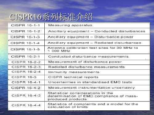
天线
4.天线的增益 天线增益是用来衡量天线朝一个特定方向收发信号的能力.一般来说, 增益的提高主要依靠减小垂直面向辐射的波瓣宽度,而在水平面上保 持全向的辐射性能。表征天线增益的参数有dBd和dBi。dBi是相对于点 源天线的增益,在各方向的辐射是均匀的;dBd相对于对称阵子天线的 增益dBi=dBd+2.15。相同的条件下,增益越高,电波传播的距离越远。
功率 5.CISPR 16-1-4:无线电骚扰和抗扰度测量设备 辅助设备 辐射
骚扰
EMI测试仪器简述
EMI测试接收机
1.参考标准:CISPR16-1-1:2006+A1:2006+A2:2007 2.频率范围:9KHz-18GHz(Band A:9KHz-150KHz, Band B:150KHz-30MHz,
2.1.50ohm/50uH+5ohm V型AMN Freq. Range: 9KHz-150KHz
2.2. 50ohm/50uH V型AMN Freq. Range: 150KHz-30MHz
2.3. 50ohm/5uH+1ohm V型AMN Freq. Range: 150KHz-100MHz
2.4. 150ohm V型AMN Freq. Range: 150KHz-30MHz
2.5. 150ohm △型AMN Freq. Range: 150KHz-30MHz
EMI测试仪器简述
人工电源网络AMN
2.输出阻抗:50ohm 3.当输出阻抗为50ohm时,RF Att.=10dB,VSWR<=1.2-1dB 4.阻抗的模和相角 5.隔离 6.电流负载能力和串联电压降
EMI测试仪器简述
者脉冲调制骚扰测量。
二级emi参数
二级emi参数EMI,即电磁干扰(Electromagnetic Interference),是指在电子设备或电气系统中,由于电磁场的产生和传播,导致其他电子设备或电气系统正常工作受到干扰的现象。
为了保证电子设备和电气系统的正常工作,必须对其进行EMI参数设计和测试。
EMI参数是指电子设备或电气系统在设计和生产过程中需要满足的一系列特定要求。
这些参数可分为不同类别,包括辐射干扰(Radiated Emission)、传导干扰(Conducted Emission)和抗扰度(Radiated Susceptibility/Conducted Susceptibility)等。
辐射干扰是指电子设备或电气系统在工作中,产生的电磁辐射能够泄漏出来,进而对周围电子设备或电气系统产生干扰。
为了避免或减少这种干扰,需要对设备或系统的辐射干扰参数进行限制。
通常使用电磁辐射限值(Electromagnetic Radiation Limits)来表示辐射干扰的上限。
这些限值是由各国的标准组织或监管机构制定的,例如国际电工委员会(IEC)发布的CISPR 22、CISPR 25等标准。
传导干扰是指电子设备或电气系统在工作中,产生的电磁波通过电源线、信号线或接地线等传导途径对周围设备或系统产生干扰。
为了避免或减少这种干扰,需要对设备或系统的传导干扰参数进行限制。
通常使用传导限值(Conducted Emission Limits)来表示传导干扰的上限。
这些限值也是由各国的标准组织或监管机构制定的。
抗扰度是指电子设备或电气系统在受到外部电磁场的干扰时,能够正常工作而不受影响的能力。
为了保证设备或系统的正常工作,需要对其抗扰度参数进行设计和测试。
抗扰度参数包括辐射抗扰度(Radiated Susceptibility)和传导抗扰度(Conducted Susceptibility)。
辐射抗扰度是指设备或系统能够抵御外部电磁辐射干扰的能力,传导抗扰度是指设备或系统能够抵御通过电源线、信号线或接地线等传导途径引入的干扰的能力。
ScanEM 产品系列参数及配件说明书

ScanEM ®Probes—near-field probes for easy detection and measurement of electromagnetic emissionSpecificationsScanEM-C/QC AccessoriesModel CTA101Includes:Cable SMB/BNC 6’ (1.8m)BNC to Male N AdapterBNC to Banana Plug AdapterScanEM Model CTK010ScanEM-C Model CTK015ScanEM-Q Model CTK017ScanEM-QC Model CTK019ParameterEvery ScanEM kit includes:- One E field probe - One H filed probe - Plastic storage case - Batteries - User’s Guide - 6’ (1.8m) cable (models CTK015and CTK019 only)What is ScanEM ®?Shorten your development schedule and eliminate the need forproduct redesign by using proper EMC tools from the beginning of the project. ScanEM probes are diagnostic instruments for detect-ing, locating and measuring electromagnetic emission. They are professional tools that don’t require you to be an EMC expert to competently address emission compliance. Small and large compa-nies all over the world use ScanEM probes to efficiently solve EMC,signal integrity and interference problems.ScanEM probes can reliably predict electromagnetic behavior of your product, and can locate emission sources in a matter of sec-onds. They detect the presence of an electromagnetic field and pro-vide audio and visual indication of its relative strength.ScanEM probes work by themselves, or as broadband active probles with any spectrum analyzer, oscilloscope or multimeter.ScanEM FeaturesPinpoint Exact Sources of EMI Due to their high spatial reso-lution, ScanEM probes can identify the exact source of electromagnetic emission down to a single component.Detect Electric and Magnetic Fields SeparatelyKnowing the type of EM radia-tion is critical for solving emission problems. ScanEM probes can detect electric (E)and magnetic (H) fields.Small SizeScanEM probes fit in the palm of a hand and are easy to operate.Their small size allows scanning for EMI in very tight areas.Self-ContainedScanEM needs nothing else to operate as a self-containedprobe: no cords, no power sup-ply, no amplifier.Audio OutputTone pitch changes with field strength. Detect the slightest difference in the field strength without taking your eyes off the DUT.CredenceTechnologies, Inc.www ContentE Field Probe ScanEM-E ScanEM-EC ScanEM-EQ ScanEM-EQC H Field ProbeScanEM-H ScanEM-HC ScanEM-HQ ScanEM-HQC FieldsE Field Probe Electric Electric Electric Radiated Electric Radiated H Field Probe Magnetic Magnetic Magnetic Conducted Magnetic Conducted Frequency Response E Field Probe 2MHz–2GHz 2MHz–2GHz 2MHz–1GHz 2MHz–1GHz H Field Probe100kHz–100MHz1MHz–1GHz 150kHz–30MHz150kHz–30MHz RF OutputYes Yes DC Output to a Multimeter Yes Yes Sensitivity (typical) E Field Probe -10dBm/(V/m)-10dBm/(V/m)H Field Probe-20dBm/mA -12dBm/mA Dimension (approx.) 5.75"x1.21"x0.76" 6.18"x1.21"x0.76" 6.88"x1.21"x0.76"7.31"x1.21"x0.76"146mmx31mmx20mm 157mmx31mmx20mm 175mmx31mmx20mm 186mmx31mmx20mm Weight (approx.) each probe 2.25oz (65g) 2.25oz (65g) 2.3oz (70g) 2.3oz (70g)Battery (each probe)2xAAA 2xAAA 2xAAA 2xAAA (included)(included)(included)(included)Indication:LED Bar Graph 5-LED color level barAudio IndicationSpeaker (tone pitch proportional to the field strength)PC Board Level EMC Diagnostics YesYesProduct Level EMC Diagnostics YesYesSignal Integrity Yes Repair & Service YesYesProduction & QA Yes Yes EMI Location YesYes ESD Event AnalysisYesScanEM probes come with a one year limited warranty. Made in the U.S.A. All specifications are subject to change without notice.ApplicationsLED Color Bar5-LED Green/Yellow/Red light bar instantly shows relative field strength.Will Not Disturb Circuit Operation ScanEM probes do not touch the circuit and will not disturb normal operation of a tested product.Level/Squelch DialAdjust ScanEM to detect EMI in a wide dynamic range with the level dial. The squelch fea-ture keeps ScanEM quiet until it locates “hot” areas above a preset level.RF Output to Spectrum Analyzer and OscilloscopeWith their high gain andbroad, flat frequency response,ScanEM-C/QC probes provide RF signal into any spectrum analyzer or oscilloscope.DC Output to a Multimeter Monitor field strength with your multimeter: ScanEM-C/QC pro-vides DC voltage as a function of field strength.ScanEM ®—a little probe that is many things in oneEMC Diagnostics EMC in Production Service and Signal Integrity Connectivity…to a spectrum analyzerEquip your spectrum analyzer with ScanEM probes and open its eyes to signals it has never seen be-fore. Each ScanEM probe covers the entire EMC bandwidth, and has a broadband amplifier built in.Due to its high spatial resolution, ScanEM-C can pin-point a source of emission down to a trace or component.Traditional passive probes have little or no output at the lower end of the spectrum,where most fundamental frequencies are. Compare the frequency response of ScanEM probes versus their passive counterparts on the screen shot shown. ScanEM probes have a flat frequency response across the entire bandwidth.…to an oscilloscope Connected to an oscillo-scope, ScanEM-C lets you see signals without affect-ing the circuit in any way.The screenshot shows how a conventional 1GHz FET probe (bottom trace)missed signal artifacts that ScanEM-EC was able to show (top trace).ScanEM-EC, an electricfield probe, showsthe voltage on traces.ScanEM-HC, a magneticfield probe, shows AC currents up to 1GHz on…to a multimeterno additional equipment.。
二级emi参数

二级emi参数二级EMI参数:如何选择适合自己的健身计划健身已经成为现代人生活中的重要组成部分。
无论是为了保持健康、塑造身材还是追求理想的体型,选择适合自己的健身计划是至关重要的。
然而,面对琳琅满目的健身计划,很多人往往感到困惑,不知道该如何选择。
本文将为您提供一些建议,帮助您选择适合自己的健身计划。
了解自己的目标是选择适合健身计划的关键。
不同的人有不同的健身目标,例如增肌、减脂、增加柔韧性等。
了解自己的目标可以帮助我们更好地选择适合自己的健身计划。
根据自己的身体状况和健康状况选择适合的健身计划。
如果您是初学者或者身体状况不佳,建议选择一些低强度的健身计划,例如瑜伽、普拉提等。
这些运动不仅可以锻炼身体,还可以改善身体的柔韧性和平衡能力。
如果您身体状况良好,可以选择一些高强度的健身计划,例如慢跑、举重等。
这些运动可以帮助您增强肌肉力量和耐力。
选择适合自己的健身计划还需要考虑个人的喜好和兴趣。
如果您对有氧运动比较感兴趣,可以选择一些有氧运动,例如游泳、跑步等。
如果您对力量训练比较感兴趣,可以选择一些重量训练,例如举重、健身操等。
选择自己感兴趣的健身计划可以增加坚持的动力。
选择适合自己的健身计划还需要考虑时间和经济因素。
如果您的时间比较有限,可以选择一些高效的健身计划,例如间歇训练。
间歇训练可以在短时间内达到较好的效果。
如果您的经济条件允许,可以选择一些健身房或健身教练的服务,他们可以根据您的需求和目标制定专属的健身计划。
选择适合自己的健身计划需要根据个人的实际情况进行调整。
每个人的身体状况和健康状况都不同,所以健身计划也需要因人而异。
在开始健身计划之前,建议咨询专业的健身教练或医生的意见,以确保选择的健身计划对自己的身体是安全和有效的。
选择适合自己的健身计划是一项个性化的任务。
通过了解自己的目标、身体状况和健康状况,选择适合的健身计划。
同时,根据个人的喜好和兴趣选择健身计划,并考虑时间和经济因素。
最重要的是,根据个人的实际情况进行调整,确保选择的健身计划对自己的身体是安全和有效的。
- 1、下载文档前请自行甄别文档内容的完整性,平台不提供额外的编辑、内容补充、找答案等附加服务。
- 2、"仅部分预览"的文档,不可在线预览部分如存在完整性等问题,可反馈申请退款(可完整预览的文档不适用该条件!)。
- 3、如文档侵犯您的权益,请联系客服反馈,我们会尽快为您处理(人工客服工作时间:9:00-18:30)。
EMIF2MIC-68FCC
EMI FIL TER/TVS ARRA Y
Only One Name Means ProT
ek’Tion™
APPLICA TIONS
✔ Cellular Phones
✔ Notebooks
✔ Personal Digital Assistant (PDA)✔ Ground Positioning System (GPS)✔ Audio Ports
IEC COMP A TIBILITY (EN61000-4)✔ 61000-4-2 (ESD): Air - 15kV, Contact - 8kV ✔ 61000-4-4 (EFT): 40A - 5/50ns FEA TURES
✔ ESD Protection > 25 kilovolts
✔ Bidirectional EMI Filtering/TVS Low Pass Filters ✔ Low Insertion Loss: -3db Roll-Off @ 72MHz ✔ Bidirectional Configuration
✔ Protects Up to Two(2) Signal Lines
✔ RoHS Compliant on Lead-Free Versions
MECHANICAL CHARACTERISTICS ✔ 5 Bump Flip Chip Package
✔ Weight 0.73 milligrams (Approximate)✔ Available in Tin-Lead or Lead-Free Plating ✔ Solder Reflow T emperature:
Tin-Lead - Sn/Pb, 85/15: 240-245°C
Lead-Free - Sn/Ag/Cu, 96/3.5/0.5: 260-270°C
✔ Flammability Rating UL 94V-0
✔ 8mm Tape and Reel Per EIA Standard 481
05212
PIN CONFIGURA
TION
5 BUMP FC
DEVICE CHARACTERISTICS
MAXIMUM RATINGS @ 25°C Unless Otherwise Specified
Operating T emperature SYMBOL
VALUE -55°C to 150°C
°C °C -40°C to 85°C UNITS T J T STG PARAMETER Storage T emperature DC Power Per Resistor
mW 100P Typical Resistance (@ ±15% Tolerance)
OHMS
68
R
ELECTRICAL CHARACTERISTICS PER LINE @ 25°C Unless Otherwise Specified
PART NUMBER
MINIMUM BREAKDOWN VOLTAGE
@ 1mA V (BR)VOLTS MAXIMUM DIODE LEAKAGE CURRENT @ 5V I D µA TYPICAL CAPACITANCE PER LINE (See Note 1)@0V, 1 MHz
C pF
EMIF2MIC-68FCC
6.0
1
80
CUT-OFF FREQUENCY (50 Ohms I/O ZERO BIAS)
fc MHz 72
RATED STAND-OFF VOL TAGE
V WM VOLTS
5.0
MINIMUM ATTENUATION
@
800-3000 MHz
dB
30
Note 1: ±20% tolerance.
APPLICA TION INFORMA
TION
T T e m p e r a t u r e - °C
T P
0.275mm Round
Non-Solder Mask Defined Pads 0.325mm Round 0.150mm
0.330mm Round No Clean
OSP(Entek Cu Plus 106A)±50µm ±20µm
60 Seconds 270°C
Pad Size on PCB
Pad Shape Pad Definition
Solder Mask Opening Solder Stencil Thickness
Solder Stencil Aperture Opening (laser cut, 5% tapered walls)Solder Paste Type Pad Protective Finish
Tolerance - Edge To Corner Ball Solder Ball Side Coplanarity
Maximum Dwell Time Above Liquidous (183°C)Soldering Maximum Temperature
PRINTED CIRCUIT BOARD RECOMMENDATIONS
PARAMETER
VALUE
REQUIREMENTS
Temperature:
T P for Lead-Free (SnAgCu): 260-270°C T P for Tin-Lead: 240-245°C
Preheat time and temperature depends on solder paste and flux activation temperature, component size, weight, surface area &plating.
RECOMMENDED NON-SOLDER MASK
DEFINED PAD ILLUSTRATION
Solder Mask Opening
0.325mm DIA.
Solder Stencil Opening
0.330mm DIA.
P ACKAGE OUTLINE & DIMENSIONS
COPYRIGHT © Pro Tek Devices 2005
SPECIFICATIONS: ProTek reserves the right to change the electrical and or mechanical characteristics described herein without notice (except JEDEC).DESIGN CHANGES: ProTek reserves the right to discontinue product lines without notice, and that the final judgement concerning selection and
specifications is the buyer’s and that in furnishing engineering and technical assistance, ProTek assumes no responsibility with respect to the selection or specifications of such products.
ProTek Devices
2929 South Fair Lane, T empe, AZ 85282T el: 602-431-8101 Fax: 602-431-2288E-Mail: sales@ Web Site:
TAPE & REEL ORDERING NOMENCLATURE
1.Surface mount product is taped and reeled in accordance with EIA-481.
2.Plastic 8mm Tape: Suffix-T73-1 = 7 Inch Reel - 3,000 pieces per reel, i.e., EMIF2MIC-68FCC-T73-1.
3. Suffix - LF - Lead-Free, i.e., EMIF2MIC-68FCC-LF-T73-1.
Tape & Reel Specifications (Dimensions in millimeters)
D
E
P0
t
F
P2
W
1.50 ± 0.10 1.75 ± 0.10 3.50 ± 0.058.00 ±0.304.00 ±0.10
2.00 ±0.05P
4.00 ±0.100.20±0.025
A0
B0
K0
Reel Dia.Tape Width 178mm (7”)
8mm
1.08 ± 0.05 1.60 ± 0.050.72 ± 0.05。
