HD44780 LCD源程序
HD44780-LCD使用说明书-无底字

八 责任范围及维修
在您购买液晶显示模块时 精电蓬远将会为您做显示模块的检测 确保您所买的显
示模块为完好的器件 在您使用过程中因不小心将显示模块损坏 您可送至精电蓬远维
修部修理 液晶模块如果出现屏被损坏的问题 比如玻璃面破损 玻璃屏角碎裂等等
将无法进行修理 您的液晶模块只能报废
公司产品质量都是通过国际质量认证及时间的考验的 请用户放心使用 如果在使
符号
VIH VIL VOH VOL IDD
条件
IOH = 0.2 mA IOL = 1.2 mA
S
S — STN 超扭曲相列型 空缺 — TN 扭曲相列型
40466 点阵数
HT
工作温度
HV
驱动电压类型
G
STN模式: G — 黄/绿模式 S — 银色模式 B — 蓝模式 反显
F — 黑/白模式 带有补偿膜的FSTN型 D — 黑/白模式 双STN型
LED04 背光类型 LED01 LED02 LED03 LED04 EL CCFL
-2-
点阵字符型液晶显示模块使用手册
四 装配操作时的注意事项 1. 模块是经过精心设计组装而成的 请勿随意自行加工 修整 2. 金属框爪不得随意扭动 拆卸 3. 不要随意修改加工PCB板外形 装配孔 线路极其部件 4. 不得修改导电胶条 5. 不得修改任何内部支架 6. 不要碰 摔 折曲 扭动模块
V*
8+.
&$VQ&$
8+* 8+.
8CNKFFCVC V E[E'
8+* 8+.
9TKV G1R GT CVKQP
项目
使能周期 使能脉冲宽度 使能升 降时间 地址建立时间 地址保持时间 数据建立时间 数据保持时间
HD44780中文数据手册

运行时间(250Khz): 40 µs 功能:设置显示、光标及闪烁开关。 其中:D表示显示开关:D = 1为开,D = 0为关;
C表示光标开关:C = 1为开,C = 0为关; B表示闪烁开关:B = 1为开,B = 0为关。 5、光标、画面位移
运行时间(250Khz): 40 µs 功能:光标、画面移动,不影响DDRAM。 其中:S/C = 1: 画面平移一个字符位;
Tas Tah Tdsw Th
最小值 1000 450
140 10 195 10
最大值 25 -
单位 ns ns ns ns ns ns ns
项目
符号
最小值
பைடு நூலகம்最大值
单位
使能周期
TcycE
1000
-
ns
使能脉冲宽度
Pweh
450
-
ns
使能升降时间 Ter,Tef
-
25
ns
地址建立时间
Tas
140
-
ns
地址保持时间
3. 模块使用时,接入逻辑电源和驱动电源的顺序,应是先逻辑电源,后驱动电源,断电时应 先驱动电源,后逻辑电源,这样做有助于保持屏的良好显示效果和避免在上电、断电时的电压冲击 损坏。所以推荐使用带控制的DC-DC电源做为模块的驱动电源。
最透彻详细的(基于HD44780)液晶显示模组LCD1602应用(全)

有些人可能会想:为什么不全部设置为 0x00 呢?因为前面已经提过,DDRAM 中的数据 代表的是字模地址,而不是字模本身。我们看看前面的 CGROM 字模表,0x20(0b0010_0000) 恰好对应一个空白的字模(实际上,0x20 就是空格的 ASCII 码),这样也就可以清除屏幕显 示。
我们来看看相应的仿真效果,如下图所示。
0x22 0x24 0x26 0x00 0x02 显存地址
0x21 0x23 0x25 0x27 0x01
光标地址
0x40 0x67
n c z z z
z 开启移屏
运行结果似乎有点耐人寻味?怎么会是这样的呢?其实并没有错,因为我们设置了地址 自减模式,而清屏后的 AC=0,那么你再写一个数据,它减到哪里去了?就跳到第一行 DDRAM 的尾地址 0x27(而不是 0xF)。我们前面已经提过,LCD1602 只使用了 32 个 DDRAM 地址(第 一行 0x00~0xF、第二行 0x40~0x4F),所以在正常情况下,当你往 DDRAM 地址 0x27 写入 字模地址时,屏幕上是不会显示相应的字模,对不对?
为了本文的完整性,我们简单介绍一下 HD44780 中 DDRAM 的组织方式,如下图所示:
DDRAM(Display Data RAM)即“显示数据随机存取存储器”,一般我们简称为“显存”, 简单的说,你往显存中写入什么,屏幕上就会显示什么。显示位置(Display position)表示 DDRAM 地址对应的屏幕位置。例如,显示位置 1(屏幕左上角)对应 DDRAM 地址 0x00(当 然,这只是默认情况下)。
LCD原理及显示程序
在日常生活中,我们对液晶显示器并不陌生。
液晶显示模块已作为很多电子产品的通过器件,如在计算器、万用表、电子表及很多家用电子产品中都可以看到,显示的主要是数字、专用符号和图形。
在单片机的人机交流界面中,一般的输出方式有以下几种:发光管、LED 数码管、液晶显示器。
发光管和LED数码管比较常用,软硬件都比较简单,在前面章节已经介绍过,在此不作介绍,本章重点介绍字符型液晶显示器的应用。
在单片机系统中应用晶液显示器作为输出器件有以下几个优点:显示质量高由于液晶显示器每一个点在收到信号后就一直保持那种色彩和亮度,恒定发光,而不像阴极射线管显示器(CRT)那样需要不断刷新新亮点。
因此,液晶显示器画质高且不会闪烁。
数字式接口液晶显示器都是数字式的,和单片机系统的接口更加简单可靠,操作更加方便。
体积小、重量轻液晶显示器通过显示屏上的电极控制液晶分子状态来达到显示的目的,在重量上比相同显示面积的传统显示器要轻得多。
功耗低相对而言,液晶显示器的功耗主要消耗在其内部的电极和驱动IC上,因而耗电量比其它显示器要少得多。
10.8.1 液晶显示简介①液晶显示原理液晶显示的原理是利用液晶的物理特性,通过电压对其显示区域进行控制,有电就有显示,这样即可以显示出图形。
液晶显示器具有厚度薄、适用于大规模集成电路直接驱动、易于实现全彩色显示的特点,目前已经被广泛应用在便携式电脑、数字摄像机、PDA移动通信工具等众多领域。
②液晶显示器的分类液晶显示的分类方法有很多种,通常可按其显示方式分为段式、字符式、点阵式等。
除了黑白显示外,液晶显示器还有多灰度有彩色显示等。
如果根据驱动方式来分,可以分为静态驱动(Static)、单纯矩阵驱动(Simple Matrix)和主动矩阵驱动(Active Matrix)三种。
③液晶显示器各种图形的显示原理:线段的显示点阵图形式液晶由M×N个显示单元组成,假设LCD显示屏有64行,每行有128列,每8列对应1字节的8位,即每行由16字节,共16×8=128个点组成,屏上64×16个显示单元与显示RAM区1024字节相对应,每一字节的内容和显示屏上相应位置的亮暗对应。
HD44780使用手册
3
Table of Contents
1 FUNCTION AND STRUCTURE.........................................................................................................6 1.1 GENERAL .............................................................................................................................................6 1.2 CHARACTERISTICS................................................................................................................................6 1.3 HANDLING PRECAUTIONS .....................................................................................................................7 1.4 LIST OF DMC SERIES ...........................................................................................................................8 1.5 PIN ASSIGNMENTS .................................
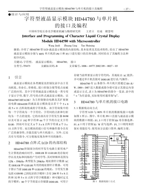
字符型液晶显示模块HD44780与单片机的接口及编程
"
$%&&#’( 点阵式 36% 的内部结构
$%&&#’( 控制部分的时序发生电路主要用来产 生计算机的响应时序、%%CAE 和 6FCAE 的存取时 序以及光标和闪烁的产生时序等, 其时钟频率范围为 典型值为 "7(G$I; 地址指针计数器 A6 8"7G H <7(G$I, 是 %%CAE 和 6FCAE 共用的地址指针计数器,可用 于指示当前 %%CAE 和 6FCAE 的地址;字符发生器 包括 6FCDE 已固化好的字模库 (含有 "(’ 种 7 B ’ 点 阵和 <" 种 7 B 88 点阵字符字模数据)和可随时定义 的字模库;’( 个字节的显示存储器 %%CAE,可用于
表, 指令名称 清屏 归 6W:5 位 输入方式设置 控制信号 12 1 3 4 *8 $ $ $ $ $ $ $ $ $ *V $ $ $ 控 *+ $ $ $ 制 *7 $ $ $
得地址线与 ()* 的 *?$ @ *?8 口进行接口的应用程 序。部分数据线接口程序如下: ABC DEF EGHEIAJ=K L MNBF O P 3 !检查 ()* 忙! 3 JEGQR (EF2CQCH S ()* 12 T $S ()* 14 T ,S ()* )2 T ,S 3 ! ()* 12 T , 为数据 U T $ 为命令 ’ ! 3 3 !()* 14 T , 为读 U T $ 为写 ’ ! 3 3 !()* )2 T , 选通 ’ ! 3
<
$%&&#’( 与单片机的接口电路
<M 8 数据线访问方式 字符型 36% 与 ’(78 单片机的数据线接口电路 如图 8 所示, 图中, 单片机 9( 口直接与液晶显示模 块的数据口相接, 98M 7 口用于控制 CK 寄存器选择, 98M > 口用于控制 C J ) 读写选择,98M # 口则用来控 制 N 使能信号, 使用该方法接口简单, 编程方便。
HD44780液晶控制器显示系统设计

第3章HD44780液晶控制器显示系统设计在电子系统设计中,离不开显示,液晶显示器(LCD)的应用更是越来越广泛。
目前主要有两种类型的液晶显示器,一种是“Alphanumaric LCDs”,只能显示字符和数字;另一种是“Graphical LCDs”,既能显示字符和数字,还能显示汉字和图形。
液晶显示器是由液晶点阵及控制器两部分组成的,不同的液晶显示器所对应的控制器不尽相同。
本章详细介绍字符液晶显示器的工作原理和应用实例。
通常,控制器和液晶屏制作在一起,也有的是分开的。
液晶屏是一种物理器件,而我们研究的控制对象是电器件,即液晶显示控制器。
所以,弄清液晶显示控制器的工作原理是应用液晶显示器必须的第一个步骤。
3.1 HD44780的工作原理HD44780是一种点阵液晶显示控制器,用来控制字符液晶显示器,目前应用比较广泛。
它有以下特点:●内置CGROM字符发生器,含192个固定字符,可供用户显示调用。
●内置CGRAM字符发生器,用户通过编程设计最多8个自定义字符,存放其中,供显示调用。
●内置DDRAM显示数据存储器,可以存放最多80个显示字符。
把CGROM 或CGRAM中的显示数据调入DDRAM,便可在显示屏上显示。
DDRAM中的单元和显示屏的位置存在一一对应关系。
●自动复位上电功能。
●双向8位或4位总线接口。
●丰富的控制指令:清显存、光标位置设置、数据输入时光标或数据移位设置、开或关显示屏等。
下面详细介绍HD44780的各项功能。
3.1.1初始化HD44780模块有两个寄存器,一个用来输入指令,另一个用来读写数据。
指令用来告诉模块怎样存放或哪里存放数据。
如果模块上电时,上升沿时间满足图3-1所示的要求,则模块缺省执行内置的上电初始化程序如下:●清显存●功能设置(DL=1,8位接口;N=0,单行显示;F=0,5×7点阵字体)●显示开关控制(D=0,关闭显示;C=0,关闭光标;B=0,字符闪烁关闭)●输入方式设置(I/D=1,设DDRAM计数器为自动加1方式)●DDRAM被选择注:括号中的内容见表3-2。
lcd段码屏驱动原理

lcd段码屏驱动原理
LCD段码屏是一种常见的数字显示设备,它的驱动原理主要涉及到显示控制芯片和显示模块两个方面。
1. 显示控制芯片
LCD段码屏的显示控制芯片通常采用CMOS技术制造,它可以通过内部的控制逻辑和存储器,控制LCD每一段的电压信号,从而实现数字图像的显示。
常见的LCD控制芯片有HD44780、KS0108、KS0066等,其中HD44780是一种具有广泛应用的标准控制芯片。
2. 显示模块
LCD段码屏的显示模块由多个LCD段组成,每个LCD段由数根独立的导电柱和两根金属屏蔽板组成,通过在导电柱和金属屏蔽板之间加电压差,实现液晶分子的定向排列,进而改变透射光的相位差,实现数字图像的显示。
在不同的电压条件下,液晶分子的定向状态也不同,对应不同的显示状态。
因此,通过控制每一段的电压信号,就可以实现数字图像的显示。
总结:
LCD段码屏的驱动原理主要包括显示控制芯片和显示模块两个方面。
通过控制每一段的电压信号,就可以实现数字图像的显示。
海量的应用场景,让段码屏成为了数字显示的中坚力量。
HD44780详解讲解

PIC单片机与基于HD44780液晶显示模块接口的设计作者:林曙光黄超昔武凌摘要:介绍了基于HD44780液晶显示模块的基本特性及其与PIC单片机的接口,并给出了常用的显示子程序。
关键词:单片机;液晶显示;接口;子程序基于HD44780的字符型液晶显示模块是一种常用的液晶显示器件,主控制驱动电路为HD44780(HITACHI),其他一些公司的电路与之全兼容,如NOVATEK 的NT3881,SAMSUNG公司的KS0066,SUNPLUS公司的SPLC78A01。
由其控制的液晶显示器可以提供若干个5×7或5×10点阵块组成的显示字符群,每个点阵块为一个字符位,字符间距和行距都为一个点的宽度,具有64 B的自定义字符RA M,可自定义8个5×8点阵字符或4个5×11点阵字符。
可以提供8×1~40×4(字符数×行数)各种显示屏规格,广泛应用于智能仪表、通讯、办公自动化及军工等领域。
1液晶显示模块的特点1.1 引脚功能表1是一种基于HD44780的液晶显示模块的引脚功能。
有些显示模块有2个使能端,这种器件可以提供多达4行的显示屏,一个使能端可以控制2行。
当RS和R/W都为低电平时可以写入指令或显示的地址;当RS为高电平、R/W为低电平时,可以写入要显示的数据;当RS为低电平、R/W 为高电平时,可以读出忙信号和地址计数器(CGRAM或DDRAM的值)。
当使能端E由高电平变为低电平时,液晶模块执行写操作(写入命令或要显示的数据、地址);D0~D7为双向数据线。
真值表如表2所示。
1.2 指令集(1)清屏功能:清显示屏,光标回到00H处。
(2)归位功能:光标复位回到00H处。
(3)输入模式设置功能:设置光标和显示模式。
其中:I/D=1时光标向右移,I/D=0时光标向左移;S=1屏幕上的文字可以移动,S=0屏幕上的文字不可以移动。
(4)显示开关控制功能:设置显示、光标及闪烁开、关。
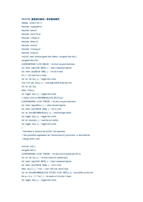
HD44780 液晶显示板的c语言驱动程序
HD44780 液晶显示板的c语言驱动程序#define _LCD44780_C#include <commdefs.h>#include "main.h"#include "lcd44780.h"#include "1306spi.h"#include "delays.h"#include "serial.h"#include "25cxxspi.h"#include "e2data.h"void lcd_send_byte(unsigned char address, unsigned char chr) {unsigned char rVal;LCDPORTDIR = LCD_READ; // set data/con port directionslcd_select_reg(CMD_REG); ); // select command registerlcd_select_dir(READ_DIR); ); // set lcd to readdo { // wait until lcd is readylcd_set_clk_hi(); (); // toggle data clockrVal = lcd_get_data(); (); // read high nibble from data buslcd_set_clk_lo();delay_500ns();lcd_toggle_clk(); (); // toggle data clock} while(!!(rVal & (HINIBBLE(LCD_BUSY))));LCDPORTDIR = LCD_WRITE; // set data/con port directionslcd_select_reg(address); ); // select desired registerlcd_select_dir(WRITE_DIR); ); // set to writelcd_set_data(HINIBBLE(chr)); )); // send the high nibblelcd_toggle_clk(); (); // toggle data clocklcd_set_data(chr); ); // send the low nibblelcd_toggle_clk(); (); // toggle data clock}// Procedure to initialise the lcd for 4 bit operation.// This procedure implements the "Initialisation by instruction" as described for// Philips PCF2116Xvoid init_lcd() {unsigned char n;LCDPORTDIR = LCD_WRITE; // set data/c on & enable port dir’nslcd_set_clk_lo(); (); // set data clock low (enable pin)lcd_select_reg(CMD_REG); ); // select command registerlcd_select_dir(WRITE_DIR); ); // set to writedelay_ms(15); ); // wait > 15ms Vdd rises above Vporlcd_set_data(HINIBBLE(LCD_FNSET | LCD_8BIT)); )); // put nibble on data bus for (n = 0; n < 3; ++n) { ) // set mode to 8 bit data 3 timeslcd_toggle_clk(); (); // toggle data clockdelay_ms(5); ); // 5ms delay}#ifdef LCD1LINES && (LCDNCHARS > 16)lcd_set_data(HINIBBLE(LCD_FNSET)); )); // set mode to 4 bit data and 1 linelcd_toggle_clk(); (); // toggle data clocklcd_send_byte(LCD_COMMAND, LCD_FNSET);#else#ifdef LCD4LINESlcd_set_data(HINIBBLE(LCD_FNSET | LCD_4LINE)); )); // set mode to 4 bit data and 4 lineslcd_toggle_clk(); (); // toggle data clocklcd_send_byte(LCD_COMMAND, LCD_FNSET | LCD_4LINE);#elselcd_set_data(HINIBBLE(LCD_FNSET | LCD_2LINE)); )); // set mode to 4 bit data and 2 lineslcd_toggle_clk(); (); // toggle data clocklcd_send_byte(LCD_COMMAND, LCD_FNSET | LCD_2LINE); ); // (applies to 16x1 also - odd one!!) #endif#endiflcd_send_byte(LCD_COMMAND, LCD_DISPON | LCD_DISP_ALL); ); // display onlcd_send_byte(LCD_COMMAND, LCD_CLR); ); // clear the displaylcd_send_byte(LCD_COMMAND, LCD_EMSET | LCD_EM_INC); ); // entry mode to increment LCDPORTDIR = LCD_READ; // set data/con port dir’nslinenum = 0; // set line number to first linedisp_blank = false; // flag display as visiblecursor_on = false; // flag the cursor as off}// Moves the cursor to posline. The first character position is 0 and the first line is 0// If the cursor bit is set then a blinking cursor location is shown else the blinking// is removed. The procedure returns the old cursor status.// Definition of posline : bits 0..4 = character position in line (left = 0)// bits 5..6 = line number (top = 0)// bit 7 = cursor status (on = 1)// In the case of single line displays the lower 6 bits are the character position.unsigned char lcd_gotoxy(unsigned char posline) {unsigned char address, cstat;cstat = cursor_on;if(c_status.prt_to_lcd) {#ifdef LCD1LINES // this method is faster than using thelinenum = 0; // modulus operator but more verboseaddress = posline & 0x3f;#elselinepos = posline & 0x1f; // save the line char positionlinenum = (posline >> 5) & 3; // save the line number#ifdef LCD2LINESif(linenum > 1) linenum = 0; // 2 line display ?#elseif(linenum > 3) linenum = 0; // 4 line display ?#endif // LCD2LINESaddress = linepos;if(linenum == 1) address += STRT_LINE2; // set ram address to (pos,line)else if(linenum == 2) address += STRT_LINE3;else if(linenum == 3) address += STRT_LINE4;#endif // LCD1LINESlcd_send_byte(LCD_COMMAND, LCD_DD_SET | address);if(!!(posline & 0x80) != cursor_on) { ) // has the cursor status changed ?cursor_on = !!(posline & 0x80);if(disp_blank) lcd_send_byte(LCD_COMMAND, LCD_DISPON);else if(cursor_on) lcd_send_byte(LCD_COMMAND, LCD_DISPON |LCD_DISP_ALL | LCD_DISP_BLNK);else lcd_send_byte(LCD_COMMAND, LCD_DISPON|LCD_DISP_ALL);}}return cstat;}// Blank or restore the display restoring the cursor status also.void lcd_blank_display(unsigned char blank) {disp_blank = blank;if(disp_blank) lcd_send_byte(LCD_COMMAND, LCD_DISPON);else if(cursor_on) lcd_send_byte(LCD_COMMAND, LCD_DISPON | LCD_DISP_ALL | LCD_DISP_BLNK); else lcd_send_byte(LCD_COMMAND, LCD_DISPON|LCD_DISP_ALL);}// If the print flag is set to lcd then writes a character to the display at cursor. Backspace,// newline and formfeed are recognised. Formfeed clears the display, newline moves the cursor// to the start of the second line. Programmable characters have codes between 0x0f and 0x1f.// They are mapped to cgram, 0x0 to 0xf. This makes all of the cgram available to programmable// characters and also allows string printing without premature termination on 0.// If the print flag is set to serial then the character is sent directly to the serial port.void putch(char chr) {if(c_status.prt_to_lcd) { ) // printing to lcdif(chr == ’\f’) {lcd_send_byte(LCD_COMMAND, LCD_CLR); ); // formfeed clears the displaylinenum = 0; // set line number to first line}// Newline to start of next line.else if(chr == ’\n’) lcd_gotoxy((cursor_on ? 0x80 : 0) | ((linenum + 1) << 5));// Return to start of current line.else if(chr == ’\r’) lcd_gotoxy((cur sor_on ? 0x80 : 0) | (linenum << 5));// Backspace.else if(chr == ’\b’) lcd_send_byte(LCD_COMMAND, LCD_SHIFT);// Other characters.else {if((chr < 0x20)&&(chr > 0x0f)) chr -= 0x10; // translate special characterslcd_send_byte(LCD_DATA, chr); ); // write at current cursor position}}else { // printing to usartif(chr == 0x11) chr = xl_super2; // translate superscript 2putch_ser(chr); ); // send char to serial portif(chr == ’\n’) putch_ser(’\r’); ); // make cr/lf pair if required}}// Clear m characters on the lcd by writing m spaces then m backspaces.void clear_line(unsigned char m) {unsigned char n = m;if(c_status.prt_to_lcd) {while(n--) lcd_send_byte(LCD_DATA, ’ ’);while(m--) lcd_send_byte(LCD_COMMAND, LCD_SHIFT);}}// Shift the screen left or right. npos is the number of character positions to shift,// +ve for right and -ve for left./*void lcd_shift(signed char npos) {unsigned char command command;command = LCD_SHIFT | LCD_DISP_SHFT SHFT;if(npos > 0) command |= LCD_SHFT_RT RT;else npos = -npos npos;while(npos--) lcd_send_byte(LCD_COMMAND, command) command);}*/// Writes a cgram character line pattern to the cgram.void lcd_write_cgram(unsigned char address, unsigned char pattern) {lcd_send_byte(LCD_COMMAND, (address & 0x3f) | LCD_CG_SET); ); // set cgram addr.lcd_send_byte(LCD_DATA, pattern);}理解HD44780兼容型LCD显示屏摘要:这篇文章试图使你能对HD44780兼容型LCD显示屏略知一二。
《液晶显示技术》配书资料:HD44780U的使用(C语言)

HD44780U的使用(C语言)字符型液晶显示模块的接口技术字符型液晶显示模块的外接口信号实际上就是HD44780U与计算机接口部的信号,信号时序为M6800系列时序。
当使用8080时序的A T89C51系列的计算机与其连接时,关键就是注意E信号的使用。
计算机与字符型液晶显示模块的连接方法有两种,一种为直接访问方式,另一种为间接控制方式。
本书将分别详细地介绍这两种方法的接口技术。
1 直接访问方式直接访问方式是计算机把字符型液晶显示模块作为存储器或I/O设备直接挂在计算机的总线上。
在这种方式下,控制信号由AT89C51的读操作信号RD和写操作信号WR与地址信号合成产生。
本文推荐的直接访问方式的实用接口电路如图1所示。
图1 直接访问方式的接口电路上图所示的电路,对于完成液晶显示模块的显示来说,所用的硬件是相对比较少的,但是如果计算机需要进行扩展的话,使用上图的话不是很经济(浪费了太多的地址空间)。
这个时候,可以考虑使用全地址译码或者部分地址译码的方式。
在上图所示的电路中:●8位数据总线与A T89C51的数据总线连接●E信号由WR和RD信号逻辑与非后产生,然后由地址A15选通控制●R/W由地址A14提供●RS信号由地址A13提供这样就确定了AT89C51操作字符型液晶显示模块的唯一地址选择。
图中的电位器为V0提供了可调的驱动电压,用以实现显示对比度的调节。
同时,上图所示的电路不经过任何改变就可以仿真出4位计算机对字符型液晶显示模块的接口,主要是驱动软件的改变。
以下将给出直接访问方式的8位和4位接口的驱动程序。
(1)地址定义#include <reg51.h>#include <intrins.h>#include <stdio.h>#define uchar unsigned char#define uint unsigned int#define nop() _nop_()xdata uchar WC_ADD _at_ 0x8000;xdata uchar RC_ADD _at_ 0xC000;xdata uchar WD_ADD _at_ 0xA000;xdata uchar RD_ADD _at_ 0xE000;(2)读入BF与AC的值8位接口:uchar RdBFAC(void){uchar status;status=RC_ADD&0x80; /*屏蔽低7位*/return status;}4位接口:uchar RdBFAC(void){uchar status,temp;status=RC_ADD;temp=RC_ADD;status=status&0x80; /*屏蔽低7位*/ return status;}(3)写指令代码8位接口:void WRCMD(uchar CMD){uchar temp;do{temp=RdBFAC();}while(temp>=0x80);WC_ADD=CMD;}4位接口:void WRCMD(uchar CMD){uchar temp;do{temp=RdBFAC();}while(temp>=0x80);WC_ADD=CMD;CMD<<=4;WC_ADD=CMD;}(4)写显示数据8位接口:void WRDAT(uchar DAT) {uchar temp;do{temp=RdBFAC();}while(temp>=0x80); WD_ADD=DAT;}4位接口:void WRDAT(uchar DAT) {uchar temp;do{temp=RdBFAC();}while(temp>=0x80); WD_ADD=DAT;DAT<<=4;WD_ADD=DAT;}(5)读显示数据8位接口:uchar RdDAT(void){uchar DAT,temp;do{temp=RdBFAC();}while(temp>=0x80);DAT=RD_ADD;return DAT;}4位接口:uchar RdDAT(void){uchar DAT,DATtemp,temp;do{temp=RdBFAC();}while(temp>=0x80);DAT=RD_ADD;DATtemp=RD_ADD;DAT=DAT|(DATtemp>>=4);return DAT;}2 间接控制方式间接控制方式是计算机把字符型液晶显示模块作为终端与计算机的并行接口连接,计算机通过对该并行接口的操作间接的实现对字符型液晶显示模块的控制。
对HD44780液晶显示器进行串行化处理

对HD44780液晶显示器进行串行化处理大部分LCD字符显示器通过像HD44780或类似控制器IC连接到外部。
但是其接口存在严重的缺点,这种LCD显示器接口占用大量微控制器的通用I/O(CPIP)管脚,而且不能提供对比度或背光强度的数字控制。
图中的电路所需的GPIO数量从11减少到2个,同时还提供LCD对比度和背光强度的数字控制。
其中采用一个通用I/O端口扩展器(U1)来仿效一个微控制器的典型8位I/O端口。
如果微控制器集成有一个I2C外围器件控制器,几乎不需要额外代码就可以实现这样的接口。
作为一种选择,可以通过正常的GPIO管脚来控制要求的信号。
运算放大器U3b对数模转换器(DAC)的输出OUT1进行缓存,OUT1控制对比度电压。
DA C输出OUT0控制由运算放大器U3A、MOSFET N1、电阻R1及R6组成的恒流阱,当D AC电压输出达到最大时,该恒流阱将汲取500mA的电流。
可以根据LCD显示尺寸来调整LED最大背光电流,可使用下列等式来计算电阻R1、R5和R6:R1=(V DD(MIN)-V FLED(MAX)-R DS(ON)*I FLED(MAX))/I FLED(MAX);P R1=I FLED(MAX)2×R1;R5=R6[(V FS(DAC)/(R1×I FLED(MAX))-1]。
这里:V DD(MIN)是最小正极电源电压(典型值4.5V);V FLED(MAX)是LED最大正向电压;I FLED(M 是LED最大正向电流;R DS(ON)是开关N1导通电阻;V FS(DAC)是DAC满刻度输出;P R1 AX)是电阻R1的最小额定功率;R6=10kΩ。
作者:Donald Schelle,美信集成产品公司。
HD44780中文数据手册

在您购买液晶显示模块时我公司将会为您做显示模块的检测,确保您所买的显示模块为完好的 器件。在您使用过程中因不小心将显示模块损坏,您可送至我公司维修,如果出现屏被损坏的问题, 将无法进行修理,只能更换玻璃。我公司将收取成本费。
液晶驱动电压:
4
RS
H/L
寄存器选择: 1: 数据寄存器; 0: 指令寄存器
5
R/W
H/L
读、写操作选择 1: 读; 0: 写
6
E
H,HÆL
使能信号 ENABLE
7
DB0
H/L
数据总线
8
DB1
H/L
数据总线
9
DB2
H/L
数据总线
10
DB3
H/L
数据总线
11
DB4
H/L
数据总线
12
DB5
H/L
数据总线
1. 模块的外引线决不允许接错,在您想调试液晶模块时,请注意正确接线,尤其是正、负电 源的接线不能有错,否则可能造成过流、过压,烧毁电路上的芯片等,对液晶模块元器件有损的现 象。
2. 模块在使用时,接入电源及断开电源必须在正电源稳定接入以后才能输入信号,电平如在 电源稳定前或断开后输入信号电平,有可能损坏模块中的IC及电路。
Tah
10
-
ns
数据延迟时间
Tddr
-
320
ns
数据保持时间
Tdhr
10
HD44780详解
PIC单片机与基于HD44780液晶显示模块接口的设计作者:林曙光黄超昔武凌摘要:介绍了基于HD44780液晶显示模块的基本特性及其与PIC单片机的接口,并给出了常用的显示子程序。
关键词:单片机;液晶显示;接口;子程序基于HD44780的字符型液晶显示模块是一种常用的液晶显示器件,主控制驱动电路为HD44780(HITACHI),其他一些公司的电路与之全兼容,如NOVATEK 的NT3881,SAMSUNG公司的KS0066,SUNPLUS公司的SPLC78A01。
由其控制的液晶显示器可以提供若干个5×7或5×10点阵块组成的显示字符群,每个点阵块为一个字符位,字符间距和行距都为一个点的宽度,具有64 B的自定义字符RA M,可自定义8个5×8点阵字符或4个5×11点阵字符。
可以提供8×1~40×4(字符数×行数)各种显示屏规格,广泛应用于智能仪表、通讯、办公自动化及军工等领域。
1液晶显示模块的特点1.1 引脚功能表1是一种基于HD44780的液晶显示模块的引脚功能。
有些显示模块有2个使能端,这种器件可以提供多达4行的显示屏,一个使能端可以控制2行。
当RS和R/W都为低电平时可以写入指令或显示的地址;当RS为高电平、R/W为低电平时,可以写入要显示的数据;当RS为低电平、R/W 为高电平时,可以读出忙信号和地址计数器(CGRAM或DDRAM的值)。
当使能端E由高电平变为低电平时,液晶模块执行写操作(写入命令或要显示的数据、地址);D0~D7为双向数据线。
真值表如表2所示。
1.2 指令集(1)清屏功能:清显示屏,光标回到00H处。
(2)归位功能:光标复位回到00H处。
(3)输入模式设置功能:设置光标和显示模式。
其中:I/D=1时光标向右移,I/D=0时光标向左移;S=1屏幕上的文字可以移动,S=0屏幕上的文字不可以移动。
(4)显示开关控制功能:设置显示、光标及闪烁开、关。
HD44780源程序
/* LCD 型号:HD44780 *//*打印机型号:EPSON M311 */#include <reg51.h>#include <absacc.h>#include <intrins.h>#define uchar unsigned char#define uint unsigned int//定义8255I/O端口地址#define PCC8255 XBYTE[0x007f] //8255命令口地址#define PC8255 XBYTE[0x007e] //8255的PC口地址#define PB8255 XBYTE[0x007d] //8255的PC口地址#define PA8255 XBYTE[0x007c] //8255的PC口地址sfr RPCTL = 0xD8;sbit RPCTL_5 = RPCTL^5;sbit LS164A = P2^5;sbit LS164cp = P2^6;sbit Print_busy = P3^3;sbit IC_RST = P1^1;sbit IC_CLK = P1^0;sbit IC_IO = P1^2;sbit IC_PGM = P3^2;uchar code table1[16]="FEDCBA9870123456";uchar code table2[16]="0000123456789ABC";void INIT_8255(void); /*初始化8255*/void LcdInit(void); /* LCD初始化函数*/void LcdCmd(uchar); /* LCD控制命令函数*/void LcdData(uchar); /* LCD数据输入函数*/void LcdClr(void); /* LCD清屏函数*/void LcdStr(uchar *); /* 显示字符串函数*/void LcdDisp(uchar x,uchar d);void Delay_msec(uint x); /* 延时函数*/uchar Getkey(void); /*键盘函数*/void PrintInit(void); /*打印初始化函数*/void PrintData (uchar d); /*打印函数*/void PrintString(uchar *p); //打印字符串void LcdDisp(uchar x,uchar d) //指定位置显示字符x:LCD位置d:字符{if(x<9){LcdCmd(0x80 + x);LcdData(d);}else{LcdCmd(0xc0 + x);LcdData(d);}}void LcdStr(uchar *p) /* 显示字符串函数*/{data uchar i;LcdCmd(0x80); //设置显示数据RAMfor (i=0;i<=7;i++){LcdData(*p); /* char of LCM */p++;}LcdCmd(0xc0); //设置显示数据RAMfor (i=0;i<=7;i++){LcdData(*p); /* char of LCM */p++;}}void LcdClr() /* LCD清屏函数 -----通过送0x20清屏*/ {data uchar i;LcdCmd(0x80); //设置显示数据RAMfor (i=0;i<=7;i++)LcdData(0x20); /* char of LCM */LcdCmd(0xc0); //设置显示数据RAMfor (i=0;i<=7;i++)LcdData(0x20); /* char of LCM */}void LcdClr1(void) /* LCD清屏函数 -----通过控制命令清屏*/ {LcdCmd(0x01);}void LcdCmd(uchar c) /* LCD控制命令函数*/{RPCTL_5 = 1;Delay_msec(1); //延时1ms (1000us)PCC8255 = 0x00;PB8255 = c ;PCC8255 = 0x05;PCC8255 = 0x04;Delay_msec(1); //延时1ms (1000us)RPCTL_5 = 0;}void LcdData(uchar c) /* LCD数据输入函数*/ {RPCTL_5 = 1;Delay_msec(1); //延时1ms (1000us)PCC8255 = 0x01;PCC8255 = 0x02;PB8255 = c;PCC8255 = 0x05;PCC8255 = 0x04;Delay_msec(1); //延时1ms (1000us)RPCTL_5 = 0;}void LcdInit() /* LCD初始化函数*/{Delay_msec(41); //延时41msLcdCmd(0x3c); //设置字符参数LcdCmd(0x08); //设置显示开/关LcdCmd(0x01); //清除显示Delay_msec(41); //延时41msLcdCmd(0x06); //设置输入方式LcdCmd(0x10); //设置显示光标移位LcdCmd(0x0c); //设置显示开/关}void Delay_msec(uint x) /* 延时函数*/{data uchar i;do{for (i=0;i<125;i++) /*延时8us x 125 = 1ms */;}while((x--)!=0);}/*-----------------------------------------------------------------*/ void INIT_8255(void) /*8255 初始化*/{_nop_ ();PCC8255 = 0x80;_nop_ ();RPCTL_5 = 0;}/*---------------------------------------------------------------*/ uchar Getkey(void){uchar i,lie,keycode,flag;flag=0;LS164A=0; //向74Ls164移入8个0for (i=0;i<8;i++){LS164cp=0;LS164cp=1;}while((P2&0x1f)==0x1f); //是否有键闭合?Delay_msec(100); //延时10ms (10,000us)while((P2&0x1f)==0x1f); //是否有键闭合?LS164A = 1; //向74Ls164移入8个1for (i=0;i<8;i++){LS164cp = 0;LS164cp = 1;}i=0;lie = 0; //lie --列号while(i<8){LS164A = 0; //向74Ls164移入0LS164cp = 0;LS164cp = 1;if((P2&0x01)==0){keycode=0x00 + lie; /*行基数= 0x00 */break;}else if((P2&0x02)==0){keycode=0x08 + lie; /*行基数= 0x08 */break;}else if((P2&0x04)==0){keycode=0x10 + lie; /*行基数= 0x10 */break;}else if((P2&0x08)==0){keycode=0x18 + lie; /*行基数= 0x18 */break;}else if((P2&0x10)==0){keycode=0x20 + lie; /*行基数= 0x20 */break;}else{ i++;lie = lie + 1; /*列号+ 1 ---下一列*/if(i==8)flag=1;}}if(flag==0){LS164A=0;for (i=0;i<8;i++){LS164cp=0;LS164cp=1;}while((P2&0x1f)!=0x1f); /*按键是否释放*/return(keycode); /*返回键码*/}elsereturn -1;}/*-------------------------------------------------------------------*/ void PrintData (uchar d) /*打印函数*/{while (Print_busy); //Busy=1,循环_nop_ ();_nop_ ();_nop_ ();_nop_ ();while (Print_busy); //Busy=1,循环RPCTL_5 = 1;PA8255 = d;PCC8255 = 0x08;PCC8255 = 0x09;RPCTL_5 = 0 ;}void PrintString(uchar *p) //打印字符串{while(*p!='\0'){PrintData(*p);p++;}PrintData(0x0a);}/*-----------------------------------------------------------------*/void PrintInit(void) /*打印初始化函数*/{uchar i;uchar code Prninitdata[12] ={0x01,0x1b,0x40,0x1b,0x55,0x25,0x1c,0x26,0x1b,0x33,0x02};for (i=0;i<11;i++)PrintData(Prninitdata[i]);}/*-----------------------------------------------------------------*/void main(){data uchar key;uchar code prn0[]=" 电脑中心";uchar code prn1[]="赵俊杰";/*************************************************************/ Delay_msec(41); //延时41msDelay_msec(41); //延时41msDelay_msec(41); //延时41msDelay_msec(41); //延时41msINIT_8255(); /*8255初始化函数*/LcdInit(); /* LCD初始化函数*/PrintInit(); /*打印初始化函数/*************************************************************/ PrintString(prn0);Delay_msec(400); //延时400msPrintString(prn1);LcdStr(table1);Getkey();LcdClr1();key = Getkey()+0x30; LcdDisp(1,key);Getkey();LcdStr(table2);Getkey();LcdClr();}。
只用一根线驱动LCD的微控制器
只用一根线驱动LCD的微控制器HD44780 LCD是嵌入系统中最常见的字母显示器。
它唯一的缺点是在4 bit模式下要使用6个I/O脚,而在8 bit模式下要用多达11个I/O脚。
以前的设计实例中曾描述过很多节省或扩展I/O脚的方法(参考文献1、参考文献2、参考文献3)。
在驱动一个HD44780兼容LCD时,最好使用基线微控制器,而不是逻辑芯片,因为微控制器成本较低,占用电路板空间较小,并且有编程特性。
Microchip推出了最小的PIC10F系列微控制器,都采用6脚SOT-23封装。
图1中的电路已证明可用于任何有管脚数限制,且必须与HD44780兼容显示器连接的嵌入系统,它只用一根单线串行链接,采用9600 波特率的简化异步RS-232协议。
该电路使用的是一片PIC10F202,但也适用于PIC10F系列中的任何成员。
但波特率高于9600时不可用,因为PIC10F202使用了1%频率容差的RC内部振荡器,而LCD对某些指令,如“清除显示”指令,要求长达1.6 ms的延迟。
参考文献:1. Raynus, Abel, “Squeeze extra outputs from a pin-limit ed microcontroller,” EDN, Aug 4, 2005, pg 96. 2.“Microcontroller provides low-cost analog-to-digital conversion, drives seven-segment displays,” EDN, May 10, 2007, pg 80. 3.Niven, Rex, “RC lowpass filter expands microcomputer’s output port,” EDN, June 21, 2007, pg 74. tips:感谢大家的阅读,本文由我司收集整编。
仅供参阅!。
HD44780

HD44780U (LCD-II)(Dot Matrix Liquid Crystal Display Controller/Driver)DescriptionThe HD44780U dot-matrix liquid crystal display controller and driver LSI displays alphanumerics, Japanese kana characters, and symbols. It can be configured to drive a dot-matrix liquid crystal display under the control of a 4- or 8-bit microprocessor. Since all the functions such as display RAM, character generator, and liquid crystal driver, required for driving a dot-matrix liquid crystal display are internally provided on one chip, a minimal system can be interfaced with this controller/driver.A single HD44780U can display up to one 8-character line or two 8-character lines.The HD44780U has pin function compatibility with the HD44780S which allows the user to easily replace an LCD-II with an HD44780U. The HD44780U character generator ROM is extended to generate 208 5 ×8 dot character fonts and 32 5 × 10 dot character fonts for a total of 240 different character fonts.The low power supply (2.7V to 5.5V) of the HD44780U is suitable for any portable battery-driven product requiring low power dissipation.Features• 5 × 8 and 5 × 10 dot matrix possible• Low power operation support:2.7 to 5.5V• Wide range of liquid crystal display driver power3.0 to 11V• Liquid crystal drive waveformA (One line frequency AC waveform)• Correspond to high speed MPU bus interface2 MHz (when V CC = 5V)• 4-bit or 8-bit MPU interface enabled• 80 × 8-bit display RAM (80 characters max.)• 9,920-bit character generator ROM for a total of 240 character fonts208 character fonts (5 × 8 dot)32 character fonts (5 × 10 dot)HD44780U• 64 × 8-bit character generator RAM8 character fonts (5 × 8 dot)4 character fonts (5 × 10 dot)• 16-common × 40-segment liquid crystal display driver• Programmable duty cycles1/8 for one line of 5 × 8 dots with cursor1/11 for one line of 5 × 10 dots with cursor1/16 for two lines of 5 × 8 dots with cursor• Wide range of instruction functions:Display clear, cursor home, display on/off, cursor on/off, display character blink, cursor shift, display shift• Pin function compatibility with HD44780S• Automatic reset circuit that initializes the controller/driver after power on• Internal oscillator with external resistors• Low power consumptionOrdering InformationType No.Package CGROMHD44780UA00FS HCD44780UA00 HD44780UA00TF FP-80BChipTFP-80FJapanese standard fontHD44780UA02FS HCD44780UA02 HD44780UA02TF FP-80BChipTFP-80FEuropean standard fontHD44780UBxxFS HCD44780UBxx HD44780UBxxTF FP-80BChipTFP-80FCustom fontNote:xx: ROM code No.HD44780U HD44780U Block DiagramHD44780UHD44780U Pin Arrangement (FP-80B)HD44780U HD44780U Pin Arrangement (TFP-80F)HD44780UHD44780U Pad ArrangementHD44780U HCD44780U Pad Location CoordinatesCoordinate CoordinatePad No.Function X (um)Y (um)Pad No.Function X (um)Y (um)1SEG22–2100231341DB22070–22902SEG21–2280231342DB32260–22903SEG20–2313208943DB42290–20994SEG19–2313183344DB52290–18835SEG18–2313161745DB62290–16676SEG17–2313140146DB72290–14527SEG16–2313118647COM12313–11868SEG15–231397048COM22313–9709SEG14–231375549COM32313–75510SEG13–231353950COM42313–53911SEG12–231332351COM52313–32312SEG11–231310852COM62313–10813SEG10–2313–10853COM7231310814SEG9–2313–32354COM8231332315SEG8–2313–53955COM9231353916SEG7–2313–75556COM10231375517SEG6–2313–97057COM11231397018SEG5–2313–118658COM122313118619SEG4–2313–140159COM132313140120SEG3–2313–161760COM142313161721SEG2–2313–183361COM152313183322SEG1–2313–207362COM162313209523GND–2280–229063SEG402296231324OSC1–2080–229064SEG392100231325OSC2–1749–229065SEG381617231326V1–1550–229066SEG371401231327V2–1268–229067SEG361186231328V3–941–229068SEG35970231329V4–623–229069SEG34755231330V5–304–229070SEG33539231331CL1–48–229071SEG32323231332CL2142–229072SEG31108231333V309–229073SEG30–1082313 CC34M475–229074SEG29–323231335D665–229075SEG28–539231336RS832–229076SEG27–755231337R/W1022–229077SEG26–970231338E1204–229078SEG25–1186231339DB01454–229079SEG24–1401231340DB11684–229080SEG23–16172313HD44780U Pin FunctionsSignal No. ofLines I/ODeviceInterfaced with FunctionRS1I MPU Selects registers.0:Instruction register (for write) Busy flag:address counter (for read)1: Data register (for write and read)R/W1I MPU Selects read or write.0:Write1:ReadE1I MPU Starts data read/write.DB4 to DB74I/O MPU Four high order bidirectional tristate data buspins. Used for data transfer and receive betweenthe MPU and the HD44780U. DB7 can be usedas a busy flag.DB0 to DB34I/O MPU Four low order bidirectional tristate data bus pins.Used for data transfer and receive between theMPU and the HD44780U.These pins are not used during 4-bit operation. CL11O Extension driver Clock to latch serial data D sent to the extensiondriverCL21O Extension driver Clock to shift serial data DM1O Extension driver Switch signal for converting the liquid crystaldrive waveform to ACD1O Extension driver Character pattern data corresponding to eachsegment signalCOM1 to COM1616O LCD Common signals that are not used are changedto non-selection waveforms. COM9 to COM16are non-selection waveforms at 1/8 duty factorand COM12 to COM16 are non-selectionwaveforms at 1/11 duty factor.SEG1 to SEG4040O LCD Segment signalsV1 to V55—Power supply Power supply for LCD driveVCC–V5 = 11 V (max)VCC , GND2—Power supply VCC: 2.7V to 5.5V, GND: 0VOSC1, OSC22—Oscillationresistor clock When crystal oscillation is performed, a resistor must be connected externally. When the pin input is an external clock, it must be input to OSC1.HD44780UFunction DescriptionRegistersThe HD44780U has two 8-bit registers, an instruction register (IR) and a data register (DR).The IR stores instruction codes, such as display clear and cursor shift, and address information for display data RAM (DDRAM) and character generator RAM (CGRAM). The IR can only be written from the MPU. The DR temporarily stores data to be written into DDRAM or CGRAM and temporarily stores data to be read from DDRAM or CGRAM. Data written into the DR from the MPU is automatically written into DDRAM or CGRAM by an internal operation. The DR is also used for data storage when reading data from DDRAM or CGRAM. When address information is written into the IR, data is read and then stored into the DR from DDRAM or CGRAM by an internal operation. Data transfer between the MPU is then completed when the MPU reads the DR. After the read, data in DDRAM or CGRAM at the next address is sent to the DR for the next read from the MPU. By the register selector (RS) signal, these two registers can be selected (Table 1).Busy Flag (BF)When the busy flag is 1, the HD44780U is in the internal operation mode, and the next instruction will not be accepted. When RS = 0 and R/W = 1 (Table 1), the busy flag is output to DB7. The next instruction must be written after ensuring that the busy flag is 0.Address Counter (AC)The address counter (AC) assigns addresses to both DDRAM and CGRAM. When an address of an instruction is written into the IR, the address information is sent from the IR to the AC. Selection of either DDRAM or CGRAM is also determined concurrently by the instruction.After writing into (reading from) DDRAM or CGRAM, the AC is automatically incremented by 1 (decremented by 1). The AC contents are then output to DB0 to DB6 when RS = 0 and R/W = 1 (Table 1). Table 1Register SelectionRS R/W Operation00IR write as an internal operation (display clear, etc.)01Read busy flag (DB7) and address counter (DB0 to DB6)10DR write as an internal operation (DR to DDRAM or CGRAM)11DR read as an internal operation (DDRAM or CGRAM to DR)HD44780UDisplay Data RAM (DDRAM)Display data RAM (DDRAM) stores display data represented in 8-bit character codes. Its extended capacity is 80 × 8 bits, or 80 characters. The area in display data RAM (DDRAM) that is not used for display can be used as general data RAM. See Figure 1 for the relationships between DDRAM addresses and positions on the liquid crystal display.) is set in the address counter (AC) as hexadecimal.The DDRAM address (ADD• 1-line display (N = 0) (Figure 2)When there are fewer than 80 display characters, the display begins at the head position. For example, if using only the HD44780, 8 characters are displayed. See Figure 3.When the display shift operation is performed, the DDRAM address shifts. See Figure 3.Figure 1 DDRAM AddressFigure 3 1-Line by 8-Character Display Example• 2-line display (N = 1) (Figure 4)Case 1: When the number of display characters is less than 40 × 2 lines, the two lines are displayed from the head. Note that the first line end address and the second line start address are notconsecutive. For example, when just the HD44780 is used, 8 characters × 2 lines are displayed. See Figure 5.When display shift operation is performed, the DDRAM address shifts. See Figure 5.Figure 4 2-Line DisplayFigure 5 2-Line by 8-Character Display ExampleCase 2: For a 16-character × 2-line display, the HD44780 can be extended using one 40-output extension driver. See Figure 6.When display shift operation is performed, the DDRAM address shifts. See Figure 6.Figure 6 2-Line by 16-Character Display ExampleCharacter Generator ROM (CGROM)The character generator ROM generates 5 × 8 dot or 5 × 10 dot character patterns from 8-bit character codes (Table 4). It can generate 208 5 × 8 dot character patterns and 32 5 × 10 dot character patterns. User-defined character patterns are also available by mask-programmed ROM.Character Generator RAM (CGRAM)In the character generator RAM, the user can rewrite character patterns by program. For 5 × 8 dots, eight character patterns can be written, and for 5 × 10 dots, four character patterns can be written.Write into DDRAM the character codes at the addresses shown as the left column of Table 4 to show the character patterns stored in CGRAM.See Table 5 for the relationship between CGRAM addresses and data and display patterns.Areas that are not used for display can be used as general data RAM.Modifying Character Patterns• Character pattern development procedureThe following operations correspond to the numbers listed in Figure 7:1.Determine the correspondence between character codes and character patterns.2.Create a listing indicating the correspondence between EPROM addresses and data.3.Program the character patterns into the EPROM.4.Send the EPROM to Hitachi.puter processing on the EPROM is performed at Hitachi to create a character pattern listing, whichis sent to the user.6.If there are no problems within the character pattern listing, a trial LSI is created at Hitachi and samplesare sent to the user for evaluation. When it is confirmed by the user that the character patterns arecorrectly written, mass production of the LSI proceeds at Hitachi.Figure 7 Character Pattern Development Procedure• Programming character patternsThis section explains the correspondence between addresses and data used to program character patterns in EPROM. The HD44780U character generator ROM can generate 208 5 × 8 dot character patterns and32 5 × 10 dot character patterns for a total of 240 different character patterns.Character patternsEPROM address data and character pattern data correspond with each other to form a 5 × 8 or 5 ×10 dot character pattern (Tables 2 and 3).Table 2Example of Correspondence between EPROM Address Data and Character Pattern(5 × 8 Dots)Cursor position Character code LinepositionNotes: 1.EPROM addresses A11 to A4 correspond to a character code.2.EPROM addresses A3 to A0 specify a line position of the character pattern.3.EPROM data O4 to O0 correspond to character pattern data.4.EPROM data O5 to O7 must be specified as 0.5. A lit display position (black) corresponds to a 1.6.Line 9 and the following lines must be blanked with 0s for a 5 × 8 dot character fonts.Handling unused character patterns1.EPROM data outside the character pattern area: Always input 0s.2.EPROM data in CGRAM area: Always input 0s. (Input 0s to EPROM addresses 00H to FFH.)3.EPROM data used when the user does not use any HD44780U character pattern: According to the userapplication, handled in one of the two ways listed as follows.a.When unused character patterns are not programmed: If an unused character code is written intoDDRAM, all its dots are lit. By not programing a character pattern, all of its bits become lit. (This is due to the EPROM being filled with 1s after it is erased.)b.When unused character patterns are programmed as 0s: Nothing is displayed even if unusedcharacter codes are written into DDRAM. (This is equivalent to a space.)Table 3Example of Correspondence between EPROM Address Data and Character Pattern(5 × 10 Dots)Cursor position Character code LinepositionNotes: 1.EPROM addresses A11 to A3 correspond to a character code.2.EPROM addresses A3 to A0 specify a line position of the character pattern.3.EPROM data O4 to O0 correspond to character pattern data.4.EPROM data O5 to O7 must be specified as 0.5. A lit display position (black) corresponds to a 1.6.Line 11 and the following lines must be blanked with 0s for a 5 × 10 dot character fonts.Note:The user can specify any pattern for character-generator RAM.Patterns (CGRAM Data)For 5 ×8 dot character patternsCharacterpattern (1)Cursor positionCharacterpattern (2)Cursor positionNotes: 1.Character code bits 0 to 2 correspond to CGRAM address bits 3 to 5 (3 bits: 8 types).2.CGRAM address bits 0 to 2 designate the character pattern line position. The 8th line is thecursor position and its display is formed by a logical OR with the cursor.Maintain the 8th line data, corresponding to the cursor display position, at 0 as the cursor display.If the 8th line data is 1, 1 bits will light up the 8th line regardless of the cursor presence.3.Character pattern row positions correspond to CGRAM data bits 0 to 4 (bit 4 being at the left).4.As shown Table 5, CGRAM character patterns are selected when character code bits 4 to 7 areall 0. However, since character code bit 3 has no effect, the R display example above can beselected by either character code 00H or 08H.5. 1 for CGRAM data corresponds to display selection and 0 to non-selection.* Indicates no effect.Patterns (CGRAM Data) (cont)Character patternCursor positionFor 5 × 10 dot character patternsNotes: 1.Character code bits 1 and 2 correspond to CGRAM address bits 4 and 5 (2 bits: 4 types).2.CGRAM address bits 0 to 3 designate the character pattern line position. The 11th line is thecursor position and its display is formed by a logical OR with the cursor.Maintain the 11th line data corresponding to the cursor display positon at 0 as the cursor display.If the 11th line data is …1“, …1“ bits will light up the 11th line regardless of the cursor presence.Since lines 12 to 16 are not used for display, they can be used for general data RAM.3.Character pattern row positions are the same as 5 × 8 dot character pattern positions.4.CGRAM character patterns are selected when character code bits 4 to 7 are all 0.However, since character code bits 0 and 3 have no effect, the P display example above can be selected by character codes 00H, 01H, 08H, and 09H.5. 1 for CGRAM data corresponds to display selection and 0 to non-selection.* Indicates no effect.Timing Generation CircuitThe timing generation circuit generates timing signals for the operation of internal circuits such as DDRAM, CGROM and CGRAM. RAM read timing for display and internal operation timing by MPU access are generated separately to avoid interfering with each other. Therefore, when writing data to DDRAM, for example, there will be no undesirable interferences, such as flickering, in areas other than the display area.Liquid Crystal Display Driver CircuitThe liquid crystal display driver circuit consists of 16 common signal drivers and 40 segment signal drivers. When the character font and number of lines are selected by a program, the required common signal drivers automatically output drive waveforms, while the other common signal drivers continue to output non-selection waveforms.Sending serial data always starts at the display data character pattern corresponding to the last address of the display data RAM (DDRAM).Since serial data is latched when the display data character pattern corresponding to the starting address enters the internal shift register, the HD44780U drives from the head display.Cursor/Blink Control CircuitThe cursor/blink control circuit generates the cursor or character blinking. The cursor or the blinking will appear with the digit located at the display data RAM (DDRAM) address set in the address counter (AC). For example (Figure 8), when the address counter is 08H, the cursor position is displayed at DDRAM address 08H.Figure 8 Cursor/Blink Display ExampleInterfacing to the MPUThe HD44780U can send data in either two 4-bit operations or one 8-bit operation, thus allowing interfacing with 4- or 8-bit MPUs.• For 4-bit interface data, only four bus lines (DB4 to DB7) are used for transfer. Bus lines DB0 to DB3 are disabled. The data transfer between the HD44780U and the MPU is completed after the 4-bit data has been transferred twice. As for the order of data transfer, the four high order bits (for 8-bit operation, DB4 to DB7) are transferred before the four low order bits (for 8-bit operation, DB0 to DB3).The busy flag must be checked (one instruction) after the 4-bit data has been transferred twice. Two more 4-bit operations then transfer the busy flag and address counter data.• For 8-bit interface data, all eight bus lines (DB0 to DB7) are used.Figure 9 4-Bit Transfer ExampleReset FunctionInitializing by Internal Reset CircuitAn internal reset circuit automatically initializes the HD44780U when the power is turned on. The following instructions are executed during the initialization. The busy flag (BF) is kept in the busy state until the initialization ends (BF = 1). The busy state lasts for 10 ms after Vrises to 4.5 V.CC1.Display clear2.Function set:DL = 1; 8-bit interface dataN = 0; 1-line displayF = 0; 5 × 8 dot character font3.Display on/off control:D = 0; Display offC = 0; Cursor offB = 0; Blinking off4.Entry mode set:I/D = 1; Increment by 1S = 0; No shiftNote:If the electrical characteristics conditions listed under the table Power Supply Conditions Using Internal Reset Circuit are not met, the internal reset circuit will not operate normally and will fail to initialize the HD44780U. For such a case, initial-ization must be performed by the MPU as explained in the section, Initializing by Instruction.InstructionsOutlineOnly the instruction register (IR) and the data register (DR) of the HD44780U can be controlled by the MPU. Before starting the internal operation of the HD44780U, control information is temporarily stored into these registers to allow interfacing with various MPUs, which operate at different speeds, or various peripheral control devices. The internal operation of the HD44780U is determined by signals sent from the MPU. These signals, which include register selection signal (RS), read/write signal (R/W), and the data bus (DB0 to DB7), make up the HD44780U instructions (Table 6). There are four categories of instructions that:• Designate HD44780U functions, such as display format, data length, etc.• Set internal RAM addresses• Perform data transfer with internal RAM• Perform miscellaneous functionsNormally, instructions that perform data transfer with internal RAM are used the most. However, auto-incrementation by 1 (or auto-decrementation by 1) of internal HD44780U RAM addresses after each data write can lighten the program load of the MPU. Since the display shift instruction (Table 11) can perform concurrently with display data write, the user can minimize system development time with maximum programming efficiency.When an instruction is being executed for internal operation, no instruction other than the busy flag/address read instruction can be executed.Because the busy flag is set to 1 while an instruction is being executed, check it to make sure it is 0 before sending another instruction from the MPU.Note:Be sure the HD44780U is not in the busy state (BF = 0) before sending an instruction from theMPU to the HD44780U. If an instruction is sent without checking the busy flag, the time between the first instruction and next instruction will take much longer than the instruction time itself. Refer to Table 6 for the list of each instruc-tion execution time.Table 6InstructionsCodeExecution Time (max) (when f cp or Instruction RS R/W DB7DB6DB5DB4DB3DB2DB1DB0Description f OSC is 270 kHz)Clear display 01Clears entire display and sets DDRAM address 0 in address counter.Return home000000001—Sets DDRAM address 0 in address counter. Also returns display from being shifted to original position.DDRAM contents remain unchanged.1.52 msEntry mode set00000001I/D S Sets cursor move direction and specifies display shift.These operations areperformed during data write and read.37 µsDisplay on/off control 0000001D C BSets entire display (D) on/off,cursor on/off (C), and blinking of cursor position character (B).37 µs Cursor or display shift 000001S/C R/L ——Moves cursor and shifts display without changing DDRAM contents.37 µsFunction set 00001DL N F ——Sets interface data length (DL), number of display lines (N), and character font (F).37 µs SetCGRAM address 0001ACG ACG ACG ACG ACG ACG Sets CGRAM address.CGRAM data is sent and received after this setting.37 µsSetDDRAM address001ADD ADD ADD ADD ADD ADD ADD Sets DDRAM address.DDRAM data is sent and received after this setting.37 µsRead busy flag &address01BF ACACACACACACACReads busy flag (BF)indicating internal operation is being performed and reads address counter contents.0 µsTable 6Instructions (cont)Code Execution Time (max) (when fcporInstruction RS R/W DB7DB6DB5DB4DB3DB2DB1DB0Description fOSCis 270 kHz)Write data to CG or DDRAM 10Write data Writes data into DDRAM orCGRAM.37 µstADD= 4 µs*Read data from CG or DDRAM 11Read data Reads data from DDRAM orCGRAM.37 µstADD= 4 µs*I/D= 1:IncrementI/D= 0:DecrementS= 1:Accompanies display shiftS/C= 1: Display shiftS/C= 0:Cursor moveR/L= 1:Shift to the rightR/L= 0:Shift to the leftDL= 1:8 bits, DL = 0: 4 bitsN= 1: 2 lines, N = 0: 1 lineF= 1: 5 × 10 dots, F = 0: 5 × 8 dotsBF= 1:Internally operatingBF= 0: Instructions acceptableDDRAM:Display data RAMCGRAM:Character generatorRAMACG:CGRAM addressADD:DDRAM address(corresponds to cursoraddress)AC:Address counter used forboth DD and CGRAMaddressesExecution timechanges whenfrequency changesExample:When fcpor fOSCis250 kHz,37 µs × = 40 µs270250Note:— indicates no effect.*After execution of the CGRAM/DDRAM data write or read instruction, the RAM address counter is incremented or decremented by 1. The RAM address counter is updated after the busy flagturns off. In Figure 10, tADDis the time elapsed after the busy flag turns off until the address counter is updated.Figure 10 Address Counter UpdateInstruction DescriptionClear DisplayClear display writes space code 20H (character pattern for character code 20H must be a blank pattern) into all DDRAM addresses. It then sets DDRAM address 0 into the address counter, and returns the display to its original status if it was shifted. In other words, the display disappears and the cursor or blinking goes to the left edge of the display (in the first line if 2 lines are displayed). It also sets I/D to 1 (increment mode)in entry mode. S of entry mode does not change.Return HomeReturn home sets DDRAM address 0 into the address counter, and returns the display to its original status if it was shifted. The DDRAM contents do not change.The cursor or blinking go to the left edge of the display (in the first line if 2 lines are displayed).Entry Mode SetI/D: Increments (I/D = 1) or decrements (I/D = 0) the DDRAM address by 1 when a character code is written into or read from DDRAM.The cursor or blinking moves to the right when incremented by 1 and to the left when decremented by 1.The same applies to writing and reading of CGRAM.S: Shifts the entire display either to the right (I/D = 0) or to the left (I/D = 1) when S is 1. The display does not shift if S is 0.If S is 1, it will seem as if the cursor does not move but the display does. The display does not shift when reading from DDRAM. Also, writing into or reading out from CGRAM does not shift the display.Display On/Off ControlD: The display is on when D is 1 and off when D is 0. When off, the display data remains in DDRAM, but can be displayed instantly by setting D to 1.C: The cursor is displayed when C is 1 and not displayed when C is 0. Even if the cursor disappears, the function of I/D or other specifications will not change during display data write. The cursor is displayed using 5 dots in the 8th line for 5 × 8 dot character font selection and in the 11th line for the 5 × 10 dot character font selection (Figure 13).B: The character indicated by the cursor blinks when B is 1 (Figure 13). The blinking is displayed as switching between all blank dots and displayed characters at a speed of 409.6-ms intervals when f cp or f OSC is 250 kHz. The cursor and blinking can be set to display simultaneously. (The blinking frequency changes according to f OSC or the reciprocal of f cp . For example, when f cp is 270 kHz, 409.6 × 250/270 = 379.2 ms.)Cursor or Display ShiftCursor or display shift shifts the cursor position or display to the right or left without writing or reading display data (Table 7). This function is used to correct or search the display. In a 2-line display, the cursor moves to the second line when it passes the 40th digit of the first line. Note that the first and second line displays will shift at the same time.When the displayed data is shifted repeatedly each line moves only horizontally. The second line display does not shift into the first line position.The address counter (AC) contents will not change if the only action performed is a display shift. Function SetDL: Sets the interface data length. Data is sent or received in 8-bit lengths (DB7 to DB0) when DL is 1, and in 4-bit lengths (DB7 to DB4) when DL is 0.When 4-bit length is selected, data must be sent or received twice.N: Sets the number of display lines.F: Sets the character font.Note:Perform the function at the head of the program before executing any instructions (except for the read busy flag and address instruction). From this point, the function set instruction cannot be executed unless the interface data length is changed.Set CGRAM AddressSet CGRAM address sets the CGRAM address binary AAAAAA into the address counter.Data is then written to or read from the MPU for CGRAM.。
HD4478U显示LCD与51单片机驱动程序
//写数据voidLcdWD(unsignedchard){LcdWaitIdle();LCDRSPIN=1;
LCDRWPIN=0; P0=d;LCDEPIN=1; _nop_();LCDEPIN=0;}
//内部数据地址指针定位voidLcdPos(void){XPOS&=0x0f;YPOS&=0x03;
for(XPOS=x;XPOScharCharPos=-11;charCharLen=12;//滚动的字符的个数bit
LcdPause =0; //是否停止滚动
以下为字符显示位置与主程序,可相应修改。//设置str1从左边进入void
LcdLeftIn(){ delay(1500);
LCDEPIN=0;LcdWDA(2,1,str2);if(CharPos>16){CharPos=(CharLen-1)*-
HD4478U显示LCD与51单片机驱动程序
#include #include #include
sbit LbitLCDEPIN=P2;
#defineUCHARunsignedcharvoiddelay(unsignedinti){UCHARj;for(i;i>0;
式,2行,2*16*/
LcdWC(0x08);/*清除显示*/LcdWC(0x06);/*设定输入方式,增量不移位*/
LcdWC(0x0c); /*整体显示,关光标,不闪烁*/}
voidLcdWDA(unsignedcharx,unsignedchary,unsignedchar*s){YPOS=y;
tips:感谢大家的阅读,本文由我司收集整编。仅供参阅!
1; }
if(CharPos>0){LcdWDA(CharPos-1,0,”“);//前进一格清除前面的字符
HD44780详解
PIC单片机与基于HD44780液晶显示模块接口的设计作者:林曙光黄超昔武凌摘要:介绍了基于HD44780液晶显示模块的基本特性及其与PIC单片机的接口,并给出了常用的显示子程序。
关键词:单片机;液晶显示;接口;子程序基于HD44780的字符型液晶显示模块是一种常用的液晶显示器件,主控制驱动电路为HD44780(HITACHI),其他一些公司的电路与之全兼容,如NOVATEK 的NT3881,SAMSUNG公司的KS0066,SUNPLUS公司的SPLC78A01。
由其控制的液晶显示器可以提供若干个5×7或5×10点阵块组成的显示字符群,每个点阵块为一个字符位,字符间距和行距都为一个点的宽度,具有64 B的自定义字符RA M,可自定义8个5×8点阵字符或4个5×11点阵字符。
可以提供8×1~40×4(字符数×行数)各种显示屏规格,广泛应用于智能仪表、通讯、办公自动化及军工等领域。
1液晶显示模块的特点1.1 引脚功能表1是一种基于HD44780的液晶显示模块的引脚功能。
有些显示模块有2个使能端,这种器件可以提供多达4行的显示屏,一个使能端可以控制2行。
当RS和R/W都为低电平时可以写入指令或显示的地址;当RS为高电平、R/W为低电平时,可以写入要显示的数据;当RS为低电平、R/W 为高电平时,可以读出忙信号和地址计数器(CGRAM或DDRAM的值)。
当使能端E由高电平变为低电平时,液晶模块执行写操作(写入命令或要显示的数据、地址);D0~D7为双向数据线。
真值表如表2所示。
1.2 指令集(1)清屏功能:清显示屏,光标回到00H处。
(2)归位功能:光标复位回到00H处。
(3)输入模式设置功能:设置光标和显示模式。
其中:I/D=1时光标向右移,I/D=0时光标向左移;S=1屏幕上的文字可以移动,S=0屏幕上的文字不可以移动。
(4)显示开关控制功能:设置显示、光标及闪烁开、关。
- 1、下载文档前请自行甄别文档内容的完整性,平台不提供额外的编辑、内容补充、找答案等附加服务。
- 2、"仅部分预览"的文档,不可在线预览部分如存在完整性等问题,可反馈申请退款(可完整预览的文档不适用该条件!)。
- 3、如文档侵犯您的权益,请联系客服反馈,我们会尽快为您处理(人工客服工作时间:9:00-18:30)。
flag=1;
}
}
if(flag==0)
{
LS164A=0;
for (i=0;i<8;i++)
{
LS164cp=0;
LS164cp=1;
sbit Print_busy = P3^3;
sbit IC_RST = P1^1;
sbit IC_CLK = P1^0;
sbit IC_IO = P1^2;
sbit IC_PGM = P3^2;
uchar code table1[16]="FEDCBA9870123456";
PCC8255 = 0x00;
PCC8255 = 0x02;
PB8255 = c ;
PCC8255 = 0x05;
PCC8255 = 0x04;
Delay_msec(1); //延时1ms (1000us)
RPCTL_5 = 0;
}
{
LcdData(*p); /* char of LCM */
p++;
}
}
void LcdClr() /* LCD清屏函数?-----通过送0x20清屏*/
{
data uchar i;
LcdCmd(0x80); //设置显示数据RAM
while((P2&0x1f)==0x1f); //是否有键闭合?
Delay_msec(100); //延时10ms (10,000us)
while((P2&0x1f)==0x1f); //是否有键闭合?
LS164A = 1; //向74Ls164移入8个1
void PrintString(uchar *p); //打印字符串
void LcdDisp(uchar x,uchar d) //指定位置显示字符 x:LCD位置 d:字符
{
if(x<9)
{
LcdCmd(0x80 + x);
LcdData(d);
void LcdData(uchar c) /* LCD数据输入函数 */
{
RPCTL_5 = 1;
Delay_msec(1); //延时1ms (1000us)
PCC8255 = 0x01;
PCC8255 = 0x02;
PB8255 = c;
//定义8255I/O端口地址
#define PCC8255 XBYTE[0x007f] //8255命令口地址
#define PC8255 XBYTE[0x007e] //8255的PC口地址
#define PB8255 XBYTE[0x007d] //8255的PC口地址
{
keycode=0x08 + lie; /*行基数 = 0x08 */
break;
}
else if((P2&0x04)==0)
{
keycode=0x10 + lie; /*行基数 = 0x10 */
{
uchar i,lie,keycode,flag;
flag=0;
LS164A=0; //向74Ls164移入8个0
for (i=0;i<8;i++)
{
LS164cp=0;
LS164cp=1;
}
}
void LcdClr1(void) /* LCD清屏函数?-----通过控制命令清屏*/
{
LcdCmd(0x01);
}
void LcdCmd(uchar c) /* LCD控制命令函数 */
{
RPCTL_5 = 1;
Delay_msec(1); //延时1ms (1000us)
}
else
{
LcdCmd(0xc0 + x);
LcdData(d);
}
}
void LcdStr(uchar *p) /* 显示字符串函数 */
{
data uchar i;
LcdCmd(0x80); //设置显示数据RAM
LcdCmd(0x3c); //设置字符参数
LcdCmd(0x08); //设置显示开/关
LcdCmd(0x01); //清除显示
Delay_msec(41); //延时41ms
LcdCmd(0x06); //设置输入方式
LcdCmd(0x10); //设置显示光标移位
LcdCmd(0x0c); //设置显示开/关
}
void Delay_msec(uint x) /* 延时函数 */
{
data uchar i;
do
{
for (i=0;i<125;i++) /*延时 8us x 125 = 1ms */
}
while((P2&0x1f)!=0x1f); /*按键是否释放*/
return(keycode); /*返回键码 */
}
else
return -1;
}
/*-------------------------------------------------------------------*/
PCC8255 = 0x05;
PCC8255 = 0x04;
Delay_msec(1); //延时1ms (1000us)
RPCTL_5 = 0;
} Leabharlann void LcdInit() /* LCD初始化函数 */
{
Delay_msec(41); //延时41ms
#define PA8255 XBYTE[0x007c] //8255的PC口地址
sfr RPCTL = 0xD8;
sbit RPCTL_5 = RPCTL^5;
sbit LS164A = P2^5;
sbit LS164cp = P2^6;
void Delay_msec(uint x); /* 延时函数 */
uchar Getkey(void); /*键盘函数 */
void PrintInit(void); /*打印初始化函数*/
void PrintData (uchar d); /*打印函数*/
;
}
while((x--)!=0);
}
/*-----------------------------------------------------------------*/
void INIT_8255(void) /*8255 初始化 */
{
RPCTL_5 = 1;
_nop_ ();
PCC8255 = 0x80;
_nop_ ();
RPCTL_5 = 0;
}
/*---------------------------------------------------------------*/
uchar Getkey(void)
void LcdData(uchar); /* LCD数据输入函数 */
void LcdClr(void); /* LCD清屏函数 */
void LcdStr(uchar *); /* 显示字符串函数 */
void LcdDisp(uchar x,uchar d);
uchar code table2[16]="0000123456789ABC";
void INIT_8255(void); /*初始化8255*/
void LcdInit(void); /* LCD初始化函数 */
void LcdCmd(uchar); /* LCD控制命令函数 */
/* LCD 型号:HD44780 */
/*打印机型号: EPSON M311 */
#include <reg51.h>
#include <absacc.h>
#include <intrins.h>
#define uchar unsigned char
#define uint unsigned int
for (i=0;i<8;i++)
{
LS164cp = 0;
LS164cp = 1;
}
i=0;
lie = 0; //lie --列号
while(i<8)
{
LS164A = 0; //向74Ls164移入0
{
keycode=0x20 + lie; /*行基数 = 0x20 */
break;
}
else
{ i++;
lie = lie + 1; /*列号 + 1 ---下一列*/
for (i=0;i<=7;i++)
LcdData(0x20); /* char of LCM */
LcdCmd(0xc0); //设置显示数据RAM
for (i=0;i<=7;i++)
LcdData(0x20); /* char of LCM */
LS164cp = 0;
LS164cp = 1;
if((P2&0x01)==0)
{
keycode=0x00 + lie; /*行基数 = 0x00 */