Indium solder paste datasheet
锡膏剖析

如何正確 使用锡 如何正確地使用锡膏 ? 正確地
(2)
開封后應于 8 小時內用完,否則應將未用 小時內用完, 完的锡膏扔棄 于瓶內未加到钢网上使用的锡膏﹐ 于瓶內未加到钢网上使用的锡膏﹐蓋回瓶 蓋密封﹐ 蓋密封﹐避免再冷藏 钢网上未用完之锡膏切勿回收到瓶內与未 用過的锡膏混合 添加到钢网上的锡膏應能造成滾動狀﹐ 添加到钢网上的锡膏應能造成滾動狀﹐而 不是滑動 計算每班锡膏用量﹐ 計算每班锡膏用量﹐避免取出太多來解凍
助焊剂 (松香) 之作用
氧化物是非常稳定的保護層 助焊剂內的松香能有效地分解表面氧 化物﹐令焊接面金屬暴露﹐ 化物﹐令焊接面金屬暴露﹐達至焊接 目的﹐ 目的﹐形成新金屬化合物結構 被氧化物復蓋的部份 焊盘表面 元件焊接端 錫粉表面
粘度調整剂 調整剂
粘性像果凍狀 粘性像果凍狀﹐酸碱度中性物質 俗稱為介質 ( Medium ) 作用為調整錫膏粘度﹐ 作用為調整錫膏粘度﹐改变對元 件之粘附性﹐ 件之粘附性﹐可影响锡膏暴露于 空氣中的時間長短﹐ 空氣中的時間長短﹐同時亦改变 锡膏之抗崩塌性
錫粉顆粒 (1)
合金成份----合金成份----- 可分作兩大类 有鉛…… Sn/Pb 63/37
Sn/Pb/Ag 62/36/2 95.5/3.8/0.7 95.5/4.0/0.5 95.5/3.9/0.6 96.2/2.5/0.8/0.5 91.8/3.4/4.8
無鉛……
Sn/Ag/Cu Sn/Ag/Cu Sn/Ag/Cu Sn/Ag/Cu/Bi Sn/Ag/Bi
助焊剂
含铅锡膏 铅锡膏 全天然树脂激活 Rosin Activated (RA) 树脂中度激活 Rosin Mildly Activated (RMA) 其它 Others 无铅锡膏 无铅锡膏 无揮發性有机化合物 VOC Free ( 水溶性 ) ( Water Soluble )
PowerWeld Inc. 铝合金焊胶和焊丝安全数据表说明书
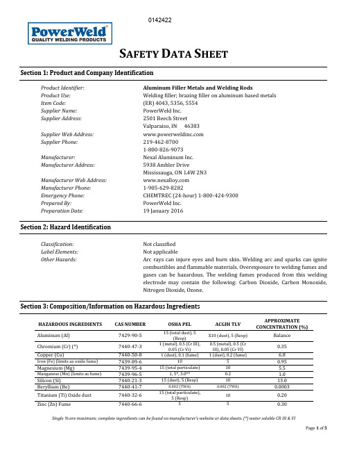
S AFETY D ATA S HEETSection 1: Product and Company IdentificationProduct Identifier:Aluminum Filler Metals and Welding RodsProduct Use: Welding filler; brazing filler on aluminum based metals Item Code: (ER) 4043, 5356, 5554 Supplier Name: PowerWeld Inc. Supplier Address: 2501 Beech StreetValparaiso, IN 46383 Supplier Web Address: Supplier Phone: 219-462-8700 1-800-826-9073 Manufacturer: Nexal Aluminum Inc. Manufacturer Address: 5938 Ambler DriveMississauga, ON L4W 2N3 Manufacturer Web Address: Manufacturer Phone: 1-905-629-8282Emergency Phone: CHEMTREC (24-hour) 1-800-424-9300 Prepared By: PowerWeld Inc. Preparation Date:19 January 2016Section 2: Hazard Identification Classification:Not classifiedLabel Elements:Not applicableOther Hazards:Arc rays can injure eyes and burn skin. Welding arc and sparks can ignite combustibles and flammable materials. Overexposure to welding fumes and gases can be hazardous. The welding fumes produced from this welding electrode may contain the following: Carbon Dioxide, Carbon Monoxide, Nitrogen Dioxide, Ozone.Section 3: Composition/Information on Hazardous IngredientsHAZARDOUS INGREDIENTS CAS NUMBER OSHA PELACGIH TLVAPPROXIMATE CONCENTRATION (%)Aluminum (Al) 7429-90-5 15 (total dust), 5(Resp)X10 (dust), 5 (Resp) Balance Chromium (Cr) (*) 7440-47-3 1 (metal), 0.5 (Cr III),0.05 (Cr Vi) 0.5 (metal), 0.5 (Cr III), 0.05 (Cr VI) 0.35 Copper (Cu)7440-50-8 1 (dust), 0.1 (fume)1 (dust), 0.2 (fume)6.8 Iron (Fe) (limits as oxide fume)7439-89-6 105 0.95 Magnesium (Mg)7439-95-4 15 (total particulate)10 5.5 Manganese (Mn) (limits as fume)7439-96-5 1, 5*, 3.0** 0.2 1.0 Silicon (Si) 7440-21-3 15 (dust), 5 (Resp)1013.0 Beryllium (Be)7440-41-7 0.002 (TWA)0.002 (TWA)0.0003 Titanium (Ti) Oxide dust 7440-32-6 15 (total particulate),5 (Resp)10 0.20 Zinc (Zn) Fume7440-66-6550.30Single % are maximum; complete ingredients can be found on manufacturer’s website or data sheets. (*) water soluble CR III & VI0142422Section 4: First-aid MeasuresInhalation:Inhalation may be the most common cause of overexposure due to thewelding fumes. Large amounts of welding fumes will cause irritation of thenose, eyes and skin. Move from the area that has any fumes to fresh air. Ifbreathing is difficult, give oxygen. If not breathing, give artificial respirationand transport to nearest medical facility for additional treatment.Ingestion:Not an expected route of exposure. Rinse month completely and drink a cupof water if conscious; obtain medical assistance when needed.Eye Contact:If arc flash or burns occur, obtain medical assistance. Large exposure towelding fumes may cause irritation to the eyes. Immediately flush upperand lower eyelids with plenty of water. After initial flushing, remove anycontact lenses and continue flushing for at least 15 minutes. Rest eyes for30 minutes. If redness, burning, blurred vision or swelling persists, visitnearest medical facility for additional treatment.Skin Contact:Large exposure to welding fumes may cause irritation to skin. If burnsoccur, flush with clean cool water for 15 minutes; obtain medical assistancewhen needed.NOTE: In all severe cases, contact physician immediately. Local telephone operators can provide number of regional poison control centre.Section 5: Fire-fighting MeasuresFlammable:NoMeans of Extinction:Not applicableAuto-ignition Temperature:Data not availableHazardous Combustion Products: Data not availableExplosion Data Sensitivity toMechanical Impact:Data not availableExplosion Data Sensitivity toStatic Discharge: Data not availableSpecial Equipment:Not applicablePrecautions for Fire Fighters:This product as shipped is non-flammable; however, fine chips and dustmay increase the explosion rating under certain heat and other ignitionhazards. Hydrogen gas and irritating fumes may form when involved in afire or if decomposing is caused from water, alcohol or sodium hydroxides.Do not use water with any molten metals and use self-contained safetyclothing/equipment in case of fires.Section 6: Accidental Release MeasuresProtection Equipment:Gloves may be worn while handling aluminum.Emergency Procedures:This product is in rod and wire form and has no hazards as shipped.Leak or Spill Procedure:If spilled, the product may be picked up (wearing gloves) and placed backinto the container. If metals become molten, contain with sand and allow toreturn back into a solid for recycle as scrap.Section 7: Handling and StorageHandling Procedures and Equipment:Proper protective gloves can be worn while handling product. During alloperations, do not eat or drink while handling and ensure properventilation while welding, brazing or processing.Storage Requirements:Store in a cool, dry and low humid location.Incompatibilities:None knownSection 8: Exposure Controls/Personal ProtectionExposure Limits:I NGREDIENTSC ANADA TWA V ALUE (MG/M3) E XPOSURE L IMITS (MG/M3) (A) (BC) (M) (O) (Q) OSHA PEL ACGIH TLVAluminum (Al) 5(p), 10(dust) 1(Resp)1(RF)1(RF)10, 5(WF)15(total dust), 5(Resp)10(dust), 1(Resp)Chromium (Cr) 0.5 0.5, 0.01 (Cr VI) 0.5 1(metal), 0.5 (Cr III),0.005 (Cr VI) 0.5(metal), 0.5 (Cr III), 0.05 (Cr VI)Copper (Cu) 1(DM), 0.2(fume) 0.2(fume) 1(DM), 0.2(fume) 1(dust), 0.1(fume) 1(dust), 0.2(fume)Iron (Fe) [oxide fume] 5(Resp)10.0(STEL), 5(FD),3(RF), 10.0(TD)5(FD)5(RF)5(FD), 10.0(TD),10(fume) 10 5Magnesium (Mg) 10(oxidefume) (box) 10.0(STEL), 3,10.0(IU)10.0(IF)10(fume) 15 (total particulate) 10Manganese (Mn) [fume] 0.2 0.1(IF),0.02(RF)0.2 3(fume)(STEL),5(dust), 1(fume) 1, 5(CL), 3.0(STEL)0.2Silicon (Si) 10.0(TD)15(dust), 5(Resp)10Beryllium (Be) 0.002 (TWA) 0.002 (TWA) Titanium (Ti) Oxide Dust 15 (totalparticulate), 5(Resp)10Zirconium 5, 10.0(STEL)5, 10.0(STEL)Zinc (Zn) Fume 2(RESP), 10.0(STEL) (Resp)2(RF), 10.0(STEL)(RF)5, 10.0(STEL),10.0(TD) 5 5Notes: (A)Canada Alberta OLEs –Occupational Health & Safety Code Schedule 1 table 2; (BC)Canada British Columbia OLEs –Occupational Exposure Limits for Chemical Substance, Occupational Health & Safety Regulation 296/97, as amended; (M) Canada Manitoba OLEs – Safety Regulation 217/2006, The workplace Safety and Health Act(MM) Respirable fraction for(M); (O)Canada Ontario OLEs –Control of Exposure to Biological or Chemical Agents; (Q)Canada Alberta OLEs –Ministry of Labor Regulation Respecting the Quality of the Work Environment; (p) Pyrophoric Powder; (CL) Ceiling Limit; (STEL) Short Term Exposure Limit; (IF) Inhalable Fraction; (FD) Fume and Dust; (TD) ;Total Dust; (box) Respirable Dust and/or Fume on Entire Box; (IU) Inhalable Fume; (Resp) Respirable; (RF)Respirable Fraction; (WF) Welding Fume; (DM ) Dust and MistEngineering Controls:Ensure proper ventilation and respiratory protection is used when welding,brazing or processing. Respiratory protection is recommended andinformation may be found regarding the OSHA STANDARDS (29 CRF1910.134), as well as CSA Standards Z94.4, along with many other safetystandards.Personal Protective Equipment:Use proper welding helmet or safety shield, as well as clothing and gloves,as required for job duties. Do not eat or drink while using these productsand wash hands after use.Section 9: Physical and Chemical PropertiesPhysical State:SolidOdour and Appearance:Odourless silver metalOdour Threshold (ppm): Not applicablepH: Not applicableMelting Point:1218°F (658°C)Freezing Point: Not applicableBoiling Point:4521°F (2494°C)Flashpoint:Not applicableUpper Flammable Limit (% by volume):Not applicableLower Flammable Limit (% by volume):Not applicableSection 10: Stability and ReactivityChemical Stability:StablePossible Hazardous Reactions:During welding, brazing and processing: fumes, dust and gas decompositionmay form.Conditions to Avoid:Avoid extreme temperaturesMaterials to Avoid (Incompatibilities):Strong acids; strong bases; strong oxidizers; metal oxides; alcohols;hydrocarbons; halogensConditions of Reactivity:Not applicableHazardous Decomposition By-Products: Not availableHazardous Polymerization:Does not occurSection 11: Toxicological InformationSkin Contact:Arc rays can burn skin; skin cancer has been reported.Skin Absorption: Not applicableEye Contact:Arc rays can injure eyes.Inhalation:Inhalation is the most likely route of exposure; refer to “Effects of AcuteExposure” and “Effects of Chronic Exposure” below.Ingestion:Unlikely due to form of product.Effects of Acute Exposure:Overexposure or inhalation of large amounts of welding fumes may causesymptoms such as metal fume fever, dizziness, nausea, dryness andirritation of your nose, throat or eyes as well as lung disease.Effects of Chronic Exposure:Overexposure or prolonged inhalation of large amounts of welding fumeswith chromium compounds may cause cancer. Other overexposure orprolonged inhalation of large amounts of welding fumes symptoms mayinclude damage to the central nervous system, respiratory system, skin andcould affect organs such as pancreas and liver.Irritancy of Product:Not availableSensitization to Product:Not availableCarcinogenicity:OSHA (29 CFR 1910.1200) lists Nickel and Chromium as possiblecarcinogens, welding fumes as possible carcinogens (2B), and hexavalentchromium as carcinogenic to humans (1) per IARC Monographs. Hexavalentchromium confirmed as human carcinogen (A1) per ACGIH and US NTPReport on CarcinogenReproductive Effects:Not availableRespiratory Sensitization:Not availableToxicological Data:Acute oral (Rat) –Manganese (LD50): 9000 mg/kg; Silicon (LD50): 3160 mg/kg Section 12: Ecological InformationAquatic and Terrestrial Toxicity:Not availablePersistence and Degradability:Not availableBioaccumulative Potential:Not availableSoil Mobility:Not availableSection 13: Disposal ConsiderationsNOTE: Always dispose of waste in accordance with local, provincial and federal regulations.Safe Handling:Gloves can be worn while handling discarded or unwanted product.Methods of Disposal:Recycle when possible. Do not allow to enter drains, sewers orwatercourses. Discard any unwanted product, residues, containers, orliners in a suitable disposal container in an environmentally acceptablemanner, as required by relevant legislation.Section 14: Transportation InformationThis material is not considered as a dangerous good per transportation regulations.Section 15: Regulatory InformationCanadian Controlled ProductsRegulations:This product has been classified according to the hazard criteria of theCanada Controlled Products Regulations, Section 33.California –Permissible ExposureLimits for Chemical Contaminants:Aluminum, Aluminum Oxide, Chromium, Copper, Magnesium, MagnesiumOxide, Manganese, Silicon, Titanium, Vanadium, Iron, Iron Oxide, Zirconium,Zinc, Zinc OxideCalifornia Proposition 65:Hexavalent chromium compounds listed in the following –a Carcinogens &Reproductive Toxic Listed Substance, Carcinogenic Substance 2/27/1987,Developmental Toxin 12/19/2008, Female Reproductive Toxin12/19/2008, Male Reproductive Toxin 12/19/2008Massachusetts – Substance Act: Aluminum, Aluminum Oxide, Chromium, Copper, Magnesium, MagnesiumOxide, Manganese, Silicon, Vanadium, Iron Oxide, Zirconium, Zinc, ZincOxideNew Jersey –Right to Know HazardousSubstance List: Aluminum, Aluminum Oxide, Chromium, Copper, Iron Oxide, HexavalentChromium compounds, Magnesium, Magnesium Oxide, Manganese, Silicon,Titanium, Titanium Oxide, Vanadium, Zinc, Zinc Oxide, Zirconium Pennsylvania – Hazardous SubstanceList: Aluminum, Aluminum oxide, Chromium, Copper, Iron oxide, Hexavalentchromium compounds , Iron oxide, Magnesium, Manganese, Silicon,Welding Fume, Vanadium, Zinc oxide and ZirconiumSection 16: Other InformationDate of Last Revision:19 January 2016Preparation Date:10 July 2015This SDS format is in accordance with GHS. PowerWeld Inc. provides the information contained herein in good faith but makes no representation as to its comprehensiveness or accuracy. This document is intended only as a guide to the appropriate precautionary handling of the material by a properly trained person using this product. Product use and conditions of use are beyond the control of PowerWeld. Warranty of materials is limited to test results of product performance as detailed in certificates of compliance. Interpretation of test results is the responsibility of end-user. No other warranties, expressed or implied, are made.。
锡膏制程管理

製表人:莫方陽
廠商: 廠商:KOKI
Lot No:004066A 每批料號 Alloy:Sn63 Pb37 錫、鉛含量 Flux : 10% 助焊劑比例 Use by □□ /□□ □□ □□/ □□ 年份 月份 日期 保存期限 Particle 20-45um 錫球顆粒大小 Net 0.5Kg 重量
備註: 備註: (1)黏度過高不易印刷,過低易流動致使印刷後之解析度降低,不但影響印刷參數與印刷品質。 黏度過高不易印刷, 黏度過高不易印刷 過低易流動致使印刷後之解析度降低,不但影響印刷參數與印刷品質。 (2)黏度之黏度量測並不容易(錫膏黏度測試機)。 黏度之黏度量測並不容易( 黏度之黏度量測並不容易 錫膏黏度測試機)
製表人:莫方陽
錫膏攪拌注意事項
6. 錫膏中之助焊劑具有不同程度之揮發性,若揮發過度 易造成錫膏 錫膏中之助焊劑具有不同程度之揮發性 若揮發過度,易造成錫膏 若揮發過度 黏度變大,甚至表面乾涸結塊而無法使用 故宜避開高溫,使用時只 甚至表面乾涸結塊而無法使用,故宜避開高溫 黏度變大 甚至表面乾涸結塊而無法使用 故宜避開高溫 使用時只 取出所需之錫膏量即可,並將瓶蓋蓋緊保持密閉 並將瓶蓋蓋緊保持密閉,使用中之錫膏亦 取出所需之錫膏量即可 並將瓶蓋蓋緊保持密閉 使用中之錫膏亦 以加罩為宜,避免置於開放空氣中 既可減少FLUX揮發 又可減少 避免置於開放空氣中,既可減少 揮發,又可減少 以加罩為宜 避免置於開放空氣中 既可減少 揮發 外界污染 7. 錫膏儲存管理以先進先出為原則 並編號管理,錫膏從冰箱取出時 錫膏儲存管理以先進先出為原則,並編號管理 錫膏從冰箱取出時 並編號管理 須登記並填寫記錄表。 須登記並填寫記錄表。 8. 印刷當中若有停止印 分鐘時,將印刷台上錫膏集中再攪拌以降 印刷當中若有停止印30分鐘時 將印刷台上錫膏集中再攪拌以降 分鐘時 低 黏度,增加印刷性 一般而言溫度每降1℃增加4%之黏度 增加印刷性(一般而言溫度每降 之黏度)。 黏度 增加印刷性 一般而言溫度每降 ℃增加 之黏度 。 9. 不同廠牌和不同成份的錫膏不得混用 如果混用錫膏須報廢。 不同廠牌和不同成份的錫膏不得混用,如果混用錫膏須報廢 如果混用錫膏須報廢。 10. 錫膏儘量減少暴露在空氣中及溼氣下使用 過程中盡快蓋上瓶蓋 錫膏儘量減少暴露在空氣中及溼氣下使用,過程中盡快蓋上瓶蓋 並避免在鋼版上有過量的錫膏。 並避免在鋼版上有過量的錫膏。 製表人:莫方陽
专有名词解释(LCD相关产业)
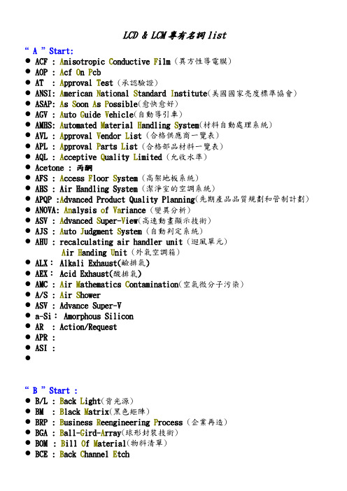
LCD & LCM專有名詞list“ A ” Start:●ACF : A nisotropic C onductive F ilm (異方性導電膜)●AOP : A cf O n P cb●AT : A pproval T est (承認驗證)●ANSI: A merican N ational S tandard I nstitute(美國國家亮度標準協會)●ASAP: A s S oon A s P ossible(愈快愈好)●AGV : A uto G uide V ehicle(自動導引車)●AMHS: A utomated M aterial H andling S ystem(材料自動處理系統)●AVL : A pproval V endor L ist (合格供應商一覽表)●APL : A pproval P arts L ist (合格部品材料一覽表)●AQL : A cceptive Q uality L imited (允收水準)●Acetone : 丙酮●AFS : A ccess F loor S ystem (高架地板系統)●AHS : Air Handling System (潔淨室的空調系統)●APQP :A dvanced Product Quality Planning(先期產品品質規劃和管制計劃) ●ANOVA: An alysis o f Va riance (變異分析)●ASV : A dvanced S uper-V iew(高速動畫顯示技術)●AJS : A uto J udgment S ystem (自動判定系統)●AHU : recalculating air handler unit (迴風單元)A ir H anding U nit (外氣空調箱)●ALX:Alkali Exhaust(鹼排氣)●AEX:Acid Exhaust(酸排氣)●AMC : A ir M athematics C ontamination(空氣微分子污染)●A/S : A ir S hower●ASV : Advance Super-V●a-Si:Amorphous Silicon●AR : Action/Request●APR :●ASI :●“ B ” Start :●B/L : B ack L ight(背光源)●BM : B lack M atrix(黑色矩陣)●BRP : B usiness R eengineering P rocess (企業再造)●BGA : B all-G ird-A rray(球形封裝技術)●BOM : B ill O f M aterial(物料清單)●BCE : B ack C hannel E tch●BRM : Basic Record Management System(基本情報管理)“ C ” Start :●CCD: C harge C oupled D evice●COB: C hip O n B oard●COF: C hip O n F ilm●COG: C hip O n G lass●CCFL: C old C athode F luorescent L amp(冷陰極射管)●CS : C ustomer S ample(顧客樣品)●CF : C olor F ilter(彩色濾光片)●CR : C ommercial R elease(量產移管)●CVD: C hemical V apour D eposition(化學氣相成長)●CIP: C ontinuous I mprovement P rocess(工程持續改善)●COA: C olor filter O n A rray ;●C ertificate O f A nalysis(供應商出貨檢驗報告)●CLCA: C lose L oop C orrective A ction●CCL: C opper C lad L aminat(銅箔基板)●CP : C apability of P rocess(製程能力指數)●CRM: C ustomer R elationnship M anage(客戶關係管理)●CIM: C omputer I ntergrated M anufacturing(電腦整合製造系統)●CAR: C orrective A ction R eport(查核改善跟催表)●CFT: C ross F unctional T eam(跨功能小組)●C/V: C on v eyer●C/R: C lean R oom●CRT: C athode R ay T ube(陰極射線管)●CGS: C eiling G rid S ystems (天板)●CDA:C lean D ry A ir (高壓乾空氣)●CAH:C omputer Room A ir H andler(恆溫恆濕空調箱) ●CWS : C hilling W ater S ystem (冰水系統)●CUB : C entral U tility B uilding (中央設施建築)●CGS : Continuous Grain Silicon●CDC :●CAS :“ D ” Start :●DAT : D esign A pproval T est(設計認定)●DVI : D igital V ideo I nteractive(數位影像穿插)●DISM: D igital I nterface S tandards for M onitors●DFP : D igital F lat P anel port●DQAT: D esign Q uality A pproval T est(設計品質認定)●DLP : D igital L ight P rocessing(數位光學處理技術)●DCC : D ocument C ontrol C enter(文件管理中心)D ry C ooling C oil(乾盤管)●DR : D esign R eview(產品設計審查)●DPT : D ew P oint T emp (露點溫度)●DI-Water: D elete-I on Water (去離子水)●EAD :●“ E ” Start :●EMS : E quipment M anagement S ystem(設備控管)●E/S : E ngineer S ample(工程樣本)●EMI : E lectro M agnetic I nterference(電磁波干擾)●ESD : E lectro S tatic D ischarge(靜電放電)●ESC : E lectro S tatic C harge(靜電電荷)●ESA : E lectro S tatic A ttraction(靜電吸附)●EMC : E lectro M agnetic C ontain(電磁相容性)●ERP : E nterprise R esource P lanning(企業資源規劃)●EL : E lectro L uminescent(電激發光)●EDID: E xtended D isplay I dentification D ata(延伸顯示識別資料) ●ECN : E ngineering C hange N otice(工程變更指示書)●ECP : E ngineering C hange P roposal (工程變更依賴書)●ERT : E mergency R esponse T eam(緊急應變小組)●EMS : E SD M onitoring S ystem (靜電氣監控系統)●EDA : E ngineering D ata A nalysis (工程資料分析)●“ F ” Start :●FPC : F lexible P rinted C ircuit(軟性印刷電路)●FET : F ield E ffect T ransistor(場效電晶體)●FI : F inal I nspection(最終檢查)●FPD : F lat P anel D isplay(平面顯示器)●FIFO: F irst I n First O ut(先進先出)●FQC : F inished goods Q uality C ontrol●FMEA: F ailure M ode E ffect A nalysis (失效模式與效應分析)●FFU : F an F ilter U nits (濾網風車組)●FFC : F an F ilter C asing●FAI : F irst A rticle I nspection (初物檢驗)●FM :F actory M utual(工廠互助保險實驗室)●FWS : F ine W ater S pray system(水霧噴水系統)●FM : F actory M utual(工廠互助保險實驗室)●FMCS: F acility M onitor C ontrol S ystem(廠務監控系統)●FMS : F acility M onitoring S ystem●FCU : F an C oil U nit (風車盤管機組)●FIB :F ocusing an I on B eam (聚焦離子束顯微鏡)●FFS : F ringe F ield S witching●FEA:Finite Element Anlysis●FAE : Facture Application (產品應用)“ G ” Start :●G/A : G ate A rray●GVIF: G igabit V ideo I nter F ace●Gage R&R(GRR) :量具(Gage)再現性(Repeatability)與再生性(Reproducibility)之變異總合●GEX:General Exhaust(一般排氣)“ H ” Start :●HTO : H igh T emperature O peration (高溫動作測試)●HAU : H anding A ssistant U nit●HEPA: H igh E fficiency P articulate A ir (高效率濾網)●HRM : H uman R esource M anagement (人力資源管理)●HEX:Heat Exhaust(熱排氣)●HVAC:General H eating V entilation A ir C ondition System(一般空調系統)●HP :Home Position●HAR :“ I ” Start :●ITO : I ndium T in O xide (氧化銦錫導電膜)●I/F : I nter-F ace (界面)●IT : I nformation T echnology (情報技術學)●IPS : I n-P lane –S witching (橫向電場切換)●ISO : I nternational S tandards O rganization (國際標準組織) ●ILB : I nner L ead B onding (內引腳接合)●IC : I ntegrated C ircuit (積體電路)●IPQC: I n-P rocess Q uality C ontrol●IQC : I ncoming Q uality C ontrol (進料品質管制)●IPA : Isopropanol alcohol (異丙醇)●IMS : I on M obility S pectrometry (離子流動分析儀)●ISP :“ J ” Start :●JIT : J ust I n T ime (即時管理)●JDM : J oint D esign M anagement (共同研發管理)“ K ” Start :●KPI :K ey P erformance I ndex (關鍵績效指標)“ L ” Start :●LCM : L iquid C rystal M odule (液晶模組)●LVDS: L ow V oltage D ifferential S ignal (低電壓差動信號)●LTO : L ow T emperature O peration (低溫動作測試)●LSI : L arge S cale I ntegration (超大型積體電路)●LC : L ine C ontroller●L/R : L aser R epair (雷射修正)●LP : L ead P itch●LCD : L iquid C rystal D isplay (液晶顯示器)●LTPS: L ow T emperature P oly S ilica (低溫多晶矽)●LGP : L ight G uide P anel (導光板)●LUX : ILLUMINATION (照明度之國際單位)●MA : M odule A ssembly (模組組裝)●MVA : M ulti-D omain V ertical A lignment(超級/多疇垂直排列)●MIS : M anagement I nformation S ystem (資訊管理系統)●MOW : M anganese O xygen W olfram (氧化錳鎢)●MTBF: M ean T ime B etween F ailure (平均失效間隔時間)●MGV : M anual G uide V ehicle (手動搬運車)●MSA : M easurement S ystem A nalysis (量測系統分析)●MAU:M ake-up A ir U nit(外氣空調箱)●MSU:M ist S eparator U nit(冷凝設備)●MSDS:M aterial S afety D ata S heet(物質安全資料表)●MDL : Manufacturing Department L●MRB : Material Review Board●MQC : M onitoring Q uality C ontrol (監控品質管制)●MCR : M aterial C onstruction R esentment(原物料品質異常工程訴怨單)●MPS : Master Product Schedule●MES : Manufacturing Execution System(製造執行系統)●MCS : Material Control System(材料管理系統)●MTD : Month To Daily vernier●MO :●“ N ” Start :●ND : N eutral D ensity filter●NB : N ote B ook●NB : N ormally B lack (常態黑)●NW : N ormally W hite (常態白)●NTSC: N ational T elevision S ystem C ommittee (國家電視標準委員會)●NC : N oise C riterion (噪音權衡基準法)●OLB : O uter L ead B onding (外引腳接合)●OD : O ptical D ensity (光學密度)●ORT : O utgoing R eliability T est (出貨信賴性測試)●OEM : O riginal E quipment M anufacturer (委託代工)●ODM : O riginal D esign M anufacture (委託設計與製造)●OLED: O RGANIC L IGHT E MITTER D EVICE (有機電激發光二極體) ●OSD : O n S creen D isplay (視控調整功能)●OQC: O ut-going Q uality C ontrol (出貨品質管制)●OPI : O ne P iece I nspection (片次檢驗)●OPI : Operation interface(操作介面)●OHS : O ver H ead S ystem (高空搬運系統)●ORP : O xidation R eduction P otential (氧化還原電位計)●OCB : O ptically C ompensated B end●ODF : O ne D rop F ill (液晶滴下方式)●OM : O ptical M icroscope (光學顯微鏡)●OEX :Organic Exhaust (有機排氣)●OITS: O perator I nterface T ouch S creen (觸摸式操作屏)●OCAP: O ut of C ontrol A ction P lan (異常反應計劃)●OOC : O ut O f C ontrol (管制外)●OOS : O ut O f S pecification (規格外)●OSS : O ne S top S hopping (一次購足)●OA : Office Automation (辦公室自動化)●OP : Opposite Position●OHV :●ORB :●OI :“ P ” Start :●PCB: P rinted C ircuit B oard (印刷電路板)●PWB: P rinted W iring B oard (印刷電路板)●PAT: P rocesses A pproval T est (製程認定)●PDAT: P rocess D esign A pproval T est (製程設計認定)●PDA: P ersonal D igital A ssistant (個人數位秘書)●PEP: P hoto E ngraving P rocess (寫真蝕刻工程)●PECVD: P hoto E ngraving C hemical V apour D eposition (化學氣相沉積)●PPM: P arts P er M illion (百萬分之…)●PZ : P olarizer (偏光板)●PE : P rocess E ngineer (製程工程師)●PMLCD:P assive M atrix LCD●PDP: P lasma D isplay P anel (電漿顯示器)●PLC: P rogrammable L ogic C ontroller (可程式化邏輯控制系統)●PNP: P lay &P lug (即插即用)●PDCA :P lan-D o-C heck-A ction (PDCA管理循環)●PSS :P roduct S pecification S heet (產品規格一覽表)●PI : Polyamide (配向膜,聚亞醘氨)●PVA: P atterned V ertical A lignment●PMS: P article M onitoring S ystem (微粒子監控系統)●PM : P roject M anagement (專案管理)●PV : P rocess V acuum System (製程真空系統)●PLV : P rocess L ow V acuum System (製程低真空系統)●PAH :P ackaged A ir H anding Unit (箱型空調箱)●PHA : P reliminary H azard A nalysis (初步危害分析)●PVA : P atterned V ertical A lignment(垂直配向)●PLM : P roduct L ife M anagement(產品生命週期管理)●PDCR: Pigment Dispersed Color Resist(顏料分散型彩色光阻)●PDM : Pigment Dispersed Method(顏料分散法)●PPI : P ixel P itch I nch“ Q ” Start :●QAT : Q uality A pproval T est (品質認定)●QCC : Q uality C ontrol C ircle (品管圈)●QOS : Q uality O f S ervice (服務品質)●QRM : Q uality R eview M eeting(服務品質)●QIT : Q uality I mprovement T eam﹝品質改善團隊﹞●QFD : Q uality F unction D eployment(品質機能展開)●QA : Q uality A ssurance (品質保證)●QC : Q uality C ontrol (品質管制)●QCS : Q uality C ontrol S tandard (品質管制標準)●QE : Q uality E ngineering (品質工程)●QMP : Q uality Management Plan (品質管制計畫)●QNR : Q uality N on-conformance R eport (原物料品質不合格報告) ●QIS :●QSM :“ R ” Start :●RTO : R oom T emperature O peration (常溫動作測試)●RMA : R eturn M aterial A uthorization (退貨驗收)●RWK : R e W or K (重工)●RSDS: R educed S wing D ifferential S ignaling●RGV : R ail G uide V ehicle(自動軌道導引車)●RTM : R otate T ransfer M achine (OHS~~stock)●RM : R isk M anagement(風險管理)●RAS : R eturn A ir S ystem (迴風系統)●RH :R elative H umidity(相對濕度)“ S ” Start :●SVGA: S uper V ideo G raphics A rray(800*600)●SXGA: S uper X tended Video G raphics A rray(1280*1024)●SXGA+: S uper X tended Video G raphics A rray PLUS(1400*1050) ●Solder:焊接(製程)●Shock:衝擊測試●STN: S uper T wisted N ematic●SPWG : S tandard P anels W orking G roup●SOP : S tandard O perating P rocedure(標準作業程序)S ystem O n P anel●SS : S uper S pacer(間隙材)●SD : S ales & D istribution(銷售管理)●SCM : S UPPLY CHAIN MANAGEMENT(供應鍊管理)●SAP : S ystemalyse A nd P rogrammentwicklung(系統分析與軟體發展)●SMT : S urface M ount T echnology(表面黏著技術)●SMD : S urface M ount D evice(表面黏裝元件)●SEM : S canning E lectron M icroscope(掃瞄式電子顯微鏡)●S.T : S tandard T ime(標準工時)●SPC : Statistical Process Control (統計製程管制)●STS : S hip T o S tock(直接入庫上線,免檢作業)●SPX : Stripper(Condensible) Exhaust(高沸點有機排氣)●SOC : Spacer on Color Filter●SOG : S ystem O n G lass●SAW : S urface A coustic W ave●SQE : S upplier Q uality E ngineering●SEX:Stripper Exhaust●SGS :●“ T ” Start :●TFT: T hin F ilm T ransistor (薄膜電晶體液晶顯示器)●TTL: T ransistor T ransistor L ogic (電晶體電晶體邏輯)●THB: T emperature H umidity B urning (高溫/高濕動作測試)●TST:T emperature S hock T est (溫度急變測試)●TCT: T emperature C ycle T est (溫度循環測試)●TAB: T ape A utomate B onding (捲帶自動接合技術)●TCP: T ape C arrier P ackage●TAC: T ri A cetyl C ellulose (三酸醋纖維)●TQM: T otal Q uality M anagement (全面品質管理實務)●TMDS: T ransition M inimized D ifferential S ignaling●TECN: T emporary E ngineering C hange N otice (暫時性工程變更指示書) ●TEG : Testing Element Group●TAT : Tact Time●TCS :●●“ U ” Start :●UV : U ltra V iolet (紫外線的..)●UXGA:U ltra S uper X tended Video G raphics A rray(1600*1200)●USB : U niversal S erial B us (萬用串列匯流排)●UWA : U ltra Wide View (超廣視角)●ULC : U ltra L ow-power C onsumption(低耗電技術)●UPS : Uninterruptible Power System (不斷電系統)●UDI : Ultra Duplex Image(單片雙影像)●UHA : Ultra High Aperture●ULPA:“ V ” Start :●Vibration:振動測試●VAC: Vac uum(真空吸著)●VGA: V ideo G raphics A rray (640*480/16色圖形之顯示模式)●VESA: V ideo E lectronic S tandard A ssociation(視訊電子標準協會)●VESDS: V ery E arly S moke D etection S ystem (極早期火警探測系統)●“ W ” Start :●WB : W hite B alance (白平衡)●WIP: W ork I n P rocess (在製品)●WI : W ork I nstruction (工作教導)●WV-Film : W ide V iew Film (廣視角膜)“ X ” Start :●XGA: X tended video G raphics A rray (1024*768) “ Y ” Start :“ Z ” Start :。
07 第七期 Solder paste introduce--Class 3
Electronics Product Class I II III
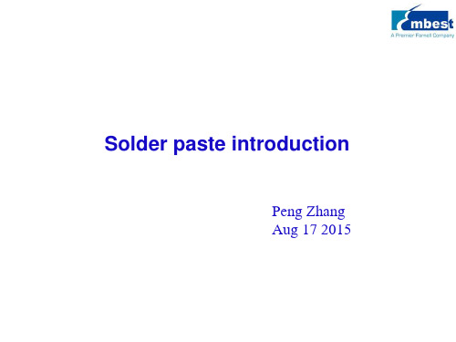
Process with post solder cleaning / 清洗工艺 Rosin/松香 Resin/树脂 Organic/有机 (RO) (RE) (OR)
L0, L1, M0, M1, H0, H1 L0, L1, M0, M1 L0, L1
Paste Classifications/锡浆的分类
Solder paste are defined by its characteristics: /从特性定义锡浆 1. Flux - Depends on criteria such as probe testable, e.g NC-Alpha OM338 助焊剂 - 依靠标准如探针可测性 例如NC-Alpha OM338
L0 L1 M0 M1 H0 H1 L0 L1 M0 M1 H0 H1 L0 L1 M0 M1 H0 H1 L0 L1 M0 M1 H0 H1
How is Flux Classified?助焊剂怎样分类
Flux Classification is Based on Material Composition and Halide Content (J-Std-004) 助焊剂分类依据材料组成成份和卤化物的含量
Solder paste introduction
Peng Zhang Aug 17 2015
Introduction to Solder Paste
Solder paste
Solder paste Jar
Paste deposite on the pad
Learning objective
2. Alloy Type - SAC 305. 合金的类型 -例如 SAC305.
高分辨率线阵相机在FPDAOI缺陷检测中的应用
光源:由于相机选型,对光源的亮度要求 不高;
设备复杂程度:很高;
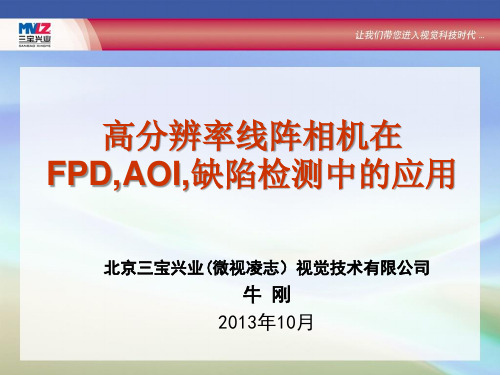
线阵AOI应用举例1: FOV:242mm,线阵相机16k分辨率, 检测精度=14.7um/pixel,镜头倍率: 0.33倍;
上图的1/8原图摘选
线阵AOI应用举例2: FOV:160mm,线阵相机16k分辨率, 检测精度=9.7um/pixel,镜头倍率: 0.5倍;
以常见的TFT-LCD液晶屏来讲,LCD是由液态晶体组成 的液晶显示屏,而LED则是由发光二极管组成的显示屏。 关键零组件包括玻璃基板、彩色滤光片、偏光片、驱动IC、 液晶材料、配向膜、背光模块、ITO导电薄膜,我们所看到 的液晶显示器是经过“模组“后的形象,模组是液晶显示 器的“后段”生产过程,顾名思义,模组二字即模块组合, 简单说共有三个步骤: • 第一步:将LCD液晶成品面板(Cell)、异方向性导电胶 (ACF)、驱动IC、柔性线路板(FPC)和PCB电路板利用机台 压合。 • 第二步:接下来和背光板、灯源、铁框一齐组装成品。 • 第三步:老化处理,经过重重检测就是我们见到的“液晶 面板了” 。
AOI行业:线阵工业相机检测应用 (1)面阵相机AOI应用简介 (2)线阵相机AOI应用的不同
概念简介:
AOI(Automatic Optic Inspection)的全称是自动光学检测,是基于 光学原理来对焊接生产中遇到的常见缺陷进行检测
PCB(Printed Circuit Board),中文名称为印制电路板 PCBA是英文Printed Circuit Board +Assembly 的简称
高分辨率线阵相机在 FPD,AOI,缺陷检测中的应用
北京三宝兴业(微视凌志)视觉技术有限公司
InvenSense AN-100 MEMS麦克风处理和组装指南说明书
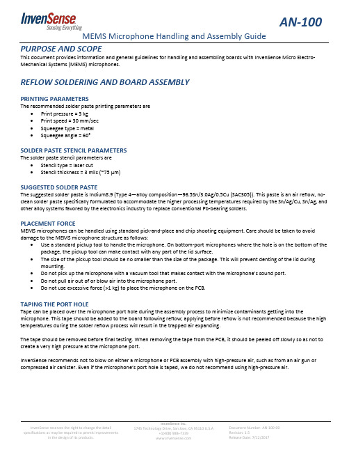
AN-100 MEMS Microphone Handling and Assembly GuideInvenSense reserves the right to change the detailInvenSense Inc.1745 Technology Drive, San Jose, CA 95110 U.S.A Document Number: AN-100-00PURPOSE AND SCOPEThis document provides information and general guidelines for handling and assembling boards with InvenSense Micro Electro-Mechanical Systems (MEMS) microphones.REFLOW SOLDERING AND BOARD ASSEMBLYPRINTING PARAMETERSThe recommended solder paste printing parameters are•Print pressure = 3 kg•Print speed = 30 mm/sec•Squeegee type = metal•Squeegee angle = 60°SOLDER PASTE STENCIL PARAMETERSThe solder paste stencil parameters are•Stencil type = laser cut•Stencil thickness = 3 mils (~75 µm)SUGGESTED SOLDER PASTEThe suggested solder paste is Indium8.9 (Type 4—alloy composition—96.5Sn/3.0Ag/0.5Cu (SAC305)). This paste is an air reflow, no-clean solder paste specifically formulated to accommodate the higher processing temperatures required by the Sn/Ag/Cu, Sn/Ag, and other alloy systems favored by the electronics industry to replace conventional Pb-bearing solders.PLACEMENT FORCEMEMS microphones can be handled using standard pick-and-place and chip shooting equipment. Care should be taken to avoid damage to the MEMS microphone structure as follows:•Use a standard pickup tool to handle the microphone. On bottom-port microphones where the hole is on the bottom of the package, the pickup tool can make contact with any part of the lid surface.•The size of the pickup tool should be no smaller than the size of the package. This will prevent denting of the lid during mounting.•Do not pick up the microphone with a vacuum tool that makes contact with the microphone’s sound port.•Do not pull air out of or blow air into the microphone port.•Do not use excessive force (>1 kg) to place the microphone on the PCB.TAPING THE PORT HOLETape can be placed over the microphone port hole during the assembly process to minimize contaminants getting into the microphone. This tape should be added to the board following reflow; applying before reflow is not recommended because the high temperatures during the solder reflow process will result in the trapped air expanding.The tape should be removed before final testing. When removing the tape from the PCB, it should be peeled off slowly so as not to create a very high pressure at the microphone port.InvenSense recommends not to blow on either a microphone or PCB assembly with high-pressure air, such as from an air gun or compressed air canister. Even if the microphone’s port hole is taped, we do not recommend using high-pressure air.AN-100REFLOW PROFILEInvenSense products are qualified in accordance with IPC/JEDEC J-STD-020D.1. This standard classifies proper packaging, storage and handling in order to avoid subsequent thermal and mechanical damage during the solder-reflow attachment phase of PCB assembly.The qualification preconditioning process specifies a sequence consisting of a bake cycle, a moisture soak cycle (in a temperature humidity oven), and three consecutive solder reflow cycles, followed by functional device testing.The peak solder reflow classification temperature requirement for package qualification is (260°C +0°C/-5°C) for lead-free soldering of components measuring less than 1.6 mm in thickness. The qualification profile and a table explaining the set points are shown below. The reflow profile in Figure 1 is recommended for board manufacturing with InvenSense MEMS microphones. These microphones are also compatible with the profile described in J-STD-020D.1.Figure 1. Recommended Soldering Profile LimitsTABLE 1. RECOMMENDED SOLDERING PROFILE LIMITSProfile FeatureSn-Pb Pb-Free Average Ramp Rate (T L to T P ) 1.25°C/sec max 1.25°C/sec max PreheatMinimum Temperature (T SMIN ) 100°C 100°C Maximum Temperature (T SMAX ) 150°C200°CTime (T SMIN to T SMAX ), t S 60 sec to 75 sec60 sec to 75 sec Ramp-Up Rate (T SMAX to T L ) 1.25°C/sec 1.25°C/sec Time Maintained Above Liquidus (t L ) 45 sec to 75 sec ~50 sec Liquidus Temperature (T L ) 183°C217°CPeak Temperature (T P )215°C +3°C/−3°C 260°C +0°C/−5°C Time Within 5°C of Actual Peak Temperature (t P ) 20 sec to 30 sec 20 sec to 30 sec Ramp-Down Rate (T P to T L )3°C/sec max 3°C/sec max Time 25°C (t 25°C ) to Peak Temperature5 minutes max5 minutes maxT E M P E R A T U R ETIMET TAN-100REWORKThe rework process of the MEMS microphone should be carried out using a rework station.1. Place the PCB with the microphone on a soldering hot plate.2. Heat the PCB so that the solder becomes liquidous.3. Use fine-tipped tweezers to remove the microphone from the PCB.4. Apply additional solder paste to pad sites using a manually operated dispensing system, such as a syringe with a small-gauge tip.5. Use a surface-mount placement machine to place the replacement component.6. Reflow the component on the rework station.CAUTIONThe MEMS microphone package has a port hole opening that is sensitive to solder flux. Do not use a vapor phase soldering process. The MEMS microphone can be damaged if subjected to cleaning processes. The cleaning solvents can enter through the port hole and damage the device.SOLDER FOOTPRINT AND PASTE MASKSFigure 2 and Figure 3 show examples of a suggested InvenSense microphone PCB land pattern and solder paste mask. See the data sheets for specific layouts for each microphone. Ensure that the PCB and solder mask design that you use follows the design rules of your specific fab and/or assembly house.Dimensions shown in millimetersDimensions shown in millimeters1.55/1.05 DIA.0.225 CUT WIDTH (2×)AN-100 HANDLING INSTRUCTIONSMEMS HANDINGUnlike conventional IC products in similar packages, MEMS devices contain moving micromechanical structures. Therefore, MEMS devices require different handling precautions than conventional ICs prior to mounting onto PCBs.InvenSense products have been qualified to a shock tolerance of 10,000g. Furthermore, the products are shipped in cushioned packaging to protect them from potential damage induced by normal handling and shipping.•Do not drop individually packaged sensors or reels of sensors.•PCBs that incorporate mounted sensors should not be separated by manually snapping apart. This could also create g-forces in excess of 10,000g.•Do not clean MEMS sensors in ultrasonic baths.•Do not open and remove MEMS devices from the moisture barrier bag until you are ready to use them. The moisture barrier bag provides good protection to the MEMS sensors during storage and transfer.•Devices dropped during handling should not be used.ESD CONSIDERATIONSEstablish and use ESD-safe handling precautions when unpacking and handling ESD-sensitive devices.•Store ESD sensitive devices in ESD safe containers until ready for use. The Tape-and-Reel moisture-sealed bag is an ESD approved barrier. The best practice is to keep the units in the original moisture sealed bags until ready for assembly. •Ensure that all workstations and personnel are properly grounded to prevent ESD. Contact InvenSense for the ESM-MM (Machine Model) rating of each individual microphone product. Restrict all device handling to ESD protected work areas that measure less than the static charge for the specific microphone’s rating.STORAGE SPECIFICATIONSInvenSense products conform to the storage specifications of IPC/JEDEC J-STD-020D.1. All InvenSense microphones are rated at MSL1 except for the INMP521, which is rated at MSL3.TABLE 2. HANDLING CONDITIONS FOR DIFFERENT MSL RATINGSRating After opening moisture-sealed bagMSL 1 Unlimited (Storage Conditions: Ambient ≤30°C at 85%RH)MSL 3 168 hours (Storage Conditions: Ambient ≤30°C at 60%RH)MSL 5 48 hours (Storage Conditions: Ambient ≤30°C at 60%RH)AN-100 PACKAGING SPECIFICATIONSTAPE AND REELFigure 4. Tape for 3.35 × 2.5 mm Packages (all dimensions in mm)Figure 7. Tape for 4.72 × 3.76 × 3.50 mm Package (all dimensions in mm)Figure 8. Tape for 3.5 × 2.65 × 0.98 mm Package (all dimensions in mm)Figure 9. Reel Outline DrawingV W102 mm 12.8 mm68 mm 12.5 mm Pin 1 OrientationUser Directionof FeedAN-100TABLE 4. REEL SPECIFICATIONSBody SizeLeadsPort LocationReel QuantityTape Pitch (mm)Pin #1Orientation7” Reel Quantity 13” Reel Quantity3.35x2.5x1.0 3 Bottom 1,000 10,000 4 B 3.35x2.5x0.98 3 Bottom 1,000 10,000 4 C 3.35x2.5x0.98 (ICS-40310) 3 Bottom 1,000 10,000 4 B 3.35x2.5x0.92 3 Bottom 1,000 10,000 4 B 3.35x2.5x0.88 3 Bottom 1,000 10,000 4 B 3.5x2.65x0.98 5 Bottom 1,000 10,000 4 B 3.5x2.65x0.98 6 Top 1,000 10,000 4 A 3.5x2.65x0.98 6 Bottom 1,000 10,000 4 B4.00x3.00x1.0 5 Bottom 1,000 5,000 8 A 4.00x3.00x1.0 7 Bottom 1,000 5,000 8 A 4.00x3.00x1.2 4 Bottom 1,000 5,000 8 C 4.72x3.76x1.0 6 Bottom 1,000 4,500 8 B 4.72x3.76x0.98 9 Bottom 1,000 4,500 8 B 4.72x3.76x3.506Bottom5002,0008BFigure 11. Example Package Marking Specification, Top View (See product data sheet for specific marking information)REEL & PIZZA BOX LABELFigure 12. Barcode Label (ICS-40310 as an example)DAAN-100Figure 13. Location of Label on ReelPACKAGINGQuantity Per Reel1,000 - 10,000 Reels per Box1 Boxes Per Carton (max) 5Pcs/Carton (max)5,000 - 50,000Figure 14. Example MSL LabelFigure 15. Moisture Sealed ReelFigure 16. Standard ESD Caution/Fragile Label on BoxMoisture Sensitivity LabelShipping LabelAN-100Pizza Box Pizza Boxes Placed in Foam- Outer Shipper LabelLined Shipper BoxFigure 17 .13” Reel Boxes and Labels7” Box 7” Reel Box in Single Small & Standard Carton Foam- Outer Shipper LabelLined Shipper BoxFigure 18 . 7” Reel Boxes and LabelsAN-100 REPRESENTATIVE SHIPPING CARTON LABELFigure 17. Outer Shipping Carton Label (MPU-9150 as an example)AN-100 REVISION HISTORYREVISION DATE REVISION DESCRIPTION7/14/2014 1.0 Initial Release11/17/2014 1.1 Updated Table 311/06/2015 1.2 Updated Table 512/10/2015 1.3 Updated Table 49/21/2016 1.4 Updated Packaging Specifications7/12/2017 1.5 Updated Packaging SpecificationsAN-100 COMPLIANCE DECLARATION DISCLAIMERInvenSense believes the environmental and other compliance information given in this document to be correct but cannot guarantee accuracy or completeness. Conformity documents substantiating the specifications and component characteristics are on file. InvenSense subcontracts manufacturing, and the information contained herein is based on data received from vendors and suppliers, which has not been validated by InvenSense.This information furnished by InvenSense, Inc. (“InvenSense”) is believed to be accurate and reliable. However, no responsibility is assumed by InvenSense for its use, or for any infringements of patents or other rights of third parties that may result from its use. Specifications are subject to change without notice. InvenSense reserves the right to make changes to this product, including its circuits and software, in order to improve its design and/or performance, without prior notice. InvenSense makes no warranties, neither expressed nor implied, regarding the information and specifications contained in this document. InvenSense assumes no responsibility for any claims or damages arising from information contained in this document, or from the use of products and services detailed therein. This includes, but is not limited to, claims or damages based on the infringement of patents, copyrights, mask work and/or other intellectual property rights.Certain intellectual property owned by InvenSense and described in this document is patent protected. No license is granted by implication or otherwise under any patent or patent rights of InvenSense. This publication supersedes and replaces all information previously supplied. Trademarks that are registered trademarks are the property of their respective companies. InvenSense sensors should not be used or sold in the development, storage, production or utilization of any conventional or mass-destructive weapons or for any other weapons or life threatening applications, as well as in any other life critical applications such as medical equipment, transportation, aerospace and nuclear instruments, undersea equipment, power plant equipment, disaster prevention and crime prevention equipment.©2017 InvenSense. All rights reserved. InvenSense, MotionTracking, MotionProcessing, MotionProcessor, MotionFusion, MotionApps, DMP, AAR, and the InvenSense logo are trademarks of InvenSense, Inc.©2017 InvenSense. All rights reserved.。
无铅锡银密封焊试验及可靠性分析
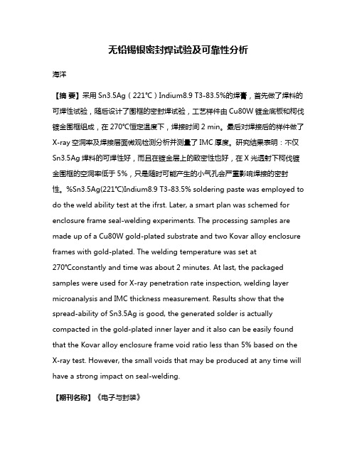
无铅锡银密封焊试验及可靠性分析海洋【摘要】采用Sn3.5Ag(221℃)Indium8.9 T3-83.5%的焊膏,首先做了焊料的可焊性试验,随后设计了围框的密封焊试验,工艺样件由Cu80W镀金底板和柯伐镀金围框组成,在270℃恒定温度下,焊接时间2 min。
最后对焊接后的样件做了X-ray空洞率及焊接层面微观检测分析并测量了IMC厚度。
研究结果表明:不仅Sn3.5Ag焊料的可焊性好,而且在镀金层上的致密性也好,在X光透射下柯伐镀金围框的空洞率低于5%,只是随时可能产生的小气孔会严重影响焊接的密封性。
%Sn3.5Ag(221℃)Indium8.9 T3-83.5% soldering paste was employed to do the weld ability test at the ifrst. Later, a smart plan was schemed for enclosure frame seal-welding experiments. The processing samples are made up of a Cu80W gold-plated substrate and two Kovar alloy enclosure frames with gold-plated. The welding temperature was set at270℃constantly and time was about 2 minutes. At last, the packaged samples were used for X-ray penetration rate inspection, welding layer microanalysis and IMC thickness measurement. Results show that the spread-ability of Sn3.5Ag is good, the generated solder is actually compacted in the gold-plated inner layer and it also can be easily found that the Kovar alloy enclosure frame void ratio less than 5% based on the X-ray test. However, the small voids that may be produced at any time will have a strong impact on seal-welding.【期刊名称】《电子与封装》【年(卷),期】2015(000)009【总页数】4页(P6-9)【关键词】Sn3.5Ag;密封焊;可焊性;X-ray;空洞率【作者】海洋【作者单位】中国电子科技集团公司第10研究所,成都 610036【正文语种】中文【中图分类】TN305.941 引言微波毫米波组件的气密封装一直是要求非常高的一项工艺技术,且封装气密性是最重要的可靠性指标之一。
SMT International生产的Chip Quik,Amtech镍酸酯合金焊接粘合剂说明书
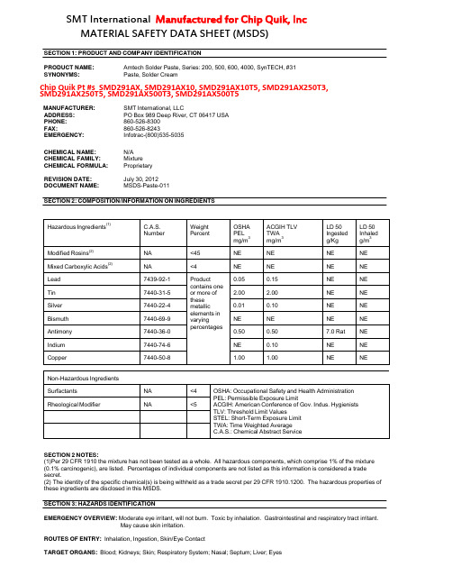
SMT International Manufactured for Chip Quik, Inc MATERIAL SAFETY DATA SHEET (MSDS)SECTION 1: PRODUCT AND COMPANY IDENTIFICATIONPRODUCT NAME: Amtech Solder Paste, Series: 200, 500, 600, 4000, SynTECH, #31 SYNONYMS: Paste, Solder CreamChip Quik Pt #s SMD291AX, SMD291AX10, SMD291AX10T5, SMD291AX250T3, SMD291AX250T5, SMD291AX500T3, SMD291AX500T5MANUFACTURER: SMT International, LLCADDRESS: PO Box 989 Deep River, CT 06417 USAPHONE: 860-526-8300FAX: 860-526-8243EMERGENCY: Infotrac-(800)535-5035CHEMICAL NAME: N/ACHEMICAL FAMILY: MixtureCHEMICAL FORMULA: ProprietaryREVISION DATE: July 30, 2012DOCUMENT NAME: MSDS-Paste-011SECTION 2: COMPOSITION/INFORMATION ON INGREDIENTSHazardous Ingredients(1) C.A.S.Number WeightPercentOSHAPELmg/m3ACGIH TLVTWAmg/m3LD 50Ingestedg/KgLD 50Inhaledg/m3Modified Rosins(2)NA <45 NE NE NE NE Mixed Carboxylic Acids(2)NA <4 NE NE NE NELead 7439-92-1 Productcontains oneor more ofthesemetallicelements invaryingpercentages 0.05 0.15 NE NETin 7440-31-5 2.00 2.00 NE NE Silver 7440-22-4 0.01 0.10 NE NE Bismuth 7440-69-9 NE NE NE NE Antimony 7440-36-0 0.50 0.50 7.0 Rat NE Indium 7440-74-6 NE 0.10 NE NE Copper 7440-50-8 1.00 1.00 NE NENon-Hazardous IngredientsSurfactants NA <4 OSHA: Occupational Safety and Health AdministrationPEL: Permissible Exposure LimitACGIH: American Conference of Gov. Indus. HygienistsTLV: Threshold Limit ValuesSTEL: Short-Term Exposure LimitTWA: Time Weighted AverageC.A.S.: Chemical Abstract ServiceRheological Modifier NA <5SECTION 2 NOTES:(1) P er 29 CFR 1910 the mixture has not been tested as a whole. All hazardous components, which comprise 1% of the mixture (0.1% carcinogenic), are listed. Percentages of individual components are not listed as this information is considered a trade secret.(2) The identity of the specific chemical(s) is being withheld as a trade secret per 29 CFR 1910.1200. The hazardous properties of these ingredients are disclosed in this MSDS.SECTION 3: HAZARDS IDENTIFICATIONEMERGENCY OVERVIEW: Moderate eye irritant, will not burn. Toxic by inhalation. Gastrointestinal and respiratory tract irritant.May cause skin irritation.ROUTES OF ENTRY: Inhalation, Ingestion, Skin/Eye ContactTARGET ORGANS: Blood; Kidneys; Skin; Respiratory System; Nasal; Septum; Liver; EyesSECTION 3: HAZARDS IDENTIFICATION (continued)MEDICAL CONDITIONS POSSIBLY AGGRAVATED BY EXPOSURE:Diseases of the blood-forming organs, kidneys, nervous and possibly reproductive systems.POTENTIAL HEALTH EFFECTSEye Contact: May cause moderate irritation, tearing, and reddening.Inhalation: Inhalation of fumes or dust may cause local irritation to the respiratory system, dizziness, weakness, fatigue, nausea, and/or headache.Skin Contact: May cause mild skin irritation.Ingestion: Harmful if swallowed. May cause irritation to the mouth, throat, and stomach. May cause abdominal discomfort, nausea, vomiting, and/or diarrhea.POTENTIAL HEALTH EFFECTS (CHRONIC and OVEREXPOSURE)Tin: Dust or fumes may cause irritation of the skin mucous membranes and may result in a benign Pneumoconiosis (Stannosis). Silver: May cause discoloration of eyes and skin (Argyia).Bismuth: May cause foul breath, a blue-black line on the gums, and Stomatitis.Antimony: May cause gastrointestinal upset, sleeplessness, irritability, and muscular pain.Indium: May cause weight loss, pulmonary edema, blood damage and degenerative changes in liver and kidneys.CHRONIC/ ACUTE HEALTH HAZARDS: Lead: Women of child-bearing age should avoid exposure to lead and its inorganic compounds due to post-natal effects. Lead can cause potential injury to a developing fetus and possible effects on reproduction. Exposure to high levels of airborne or ingested lead may produce symptoms of anemia, weakness, constipation, nausea, and abdominal pain. Prolonged exposure may result in kidney and/or nervous system involvement.CARCINOGENICITY:OSHA: N/A ACGIH: N/A NTP: N/A IARC: Lead (Pb)-Group 2BSECTION 3 NOTES:SMT International, LLC does not recommend, manufacture, market, or endorse any of its products for human consumption. Chronic Toxicity-Proposition 65, State of California: Warning! This product contains lead, known to the state of California to cause birth defects or other reproductive harm.SECTION 4: FIRST AID MEASURESEYES: Flush with water, contact a physician. Dust and/or fumes may cause irritation. If contact lenses can be removed easily, flush eyes without contact lenses. Seek medical attention if irritation persists.SKIN: After handling material wash hands thoroughly with soap and water. Dust, vapor, and/or fumes are not readily absorbed through the skin. If irritation persists, obtain medical attention.INGESTION: Seek medical attention immediately. Do not induce vomiting.INHALATION: Remove to fresh air. If breathing is difficult, seek immediate medical attention.OTHER: Lead: Excessive overexposure may result in an acute or chronic illness. If symptoms are present, the individual should be immediately removed from exposure and a physician consulted.SECTION 5: FIRE-FIGHTING MEASURESFLAMMABLE LIMITS IN AIR: N/AFLASH POINT: N/A (°F/°C)AUTOIGNITION TEMPERATURE: N/A (°F/°C)EXTINGUISHING MEDIA: Use extinguishers appropriate for conditionsSPECIAL FIRE FIGHTING PROCEDURES: Use NIOSH-approved self-contained Breathing Apparatus and full protective clothing if involved in a fire.UNUSUAL FIRE AND EXPLOSION HAZARDS: When heated to high temperatures, lead emits highly toxic fumes. HAZARDOUS DECOMPOSITION PRODUCTS: Lead oxide fumes and/or Lead particulate may be evolved.SECTION 5 NOTES:Molten solder alloys consisting of Antimony, Bismuth, Copper, Indium, Lead, Silver, and/or Tin do not produce significant quantities of fumes below 900° F.SECTION 6: ACCIDENTAL RELEASE MEASURESPRECAUTIONS AND EQUIPMENT: Material is extremely thick and will not flow out.SECTION 6: ACCIDENTAL RELEASE MEASURES (continued)ACCIDENTAL RELEASE MEASURES: If material spills or leaks use a spatula to collect spilled paste and place it in a plastic or glass jar. Remove traces of paste residue using cloth rags or paper towels moistened with Isopropyl Alcohol. Exposure to spilled material may be irritating. Follow on-site personal protective equipment recommendations.SECTION 6 NOTES:See Sections 3, 4, and 7 for additional information.SECTION 7: HANDLING AND STORAGEHANDLING: Keep containers tightly closed when not in use. Use care to avoid spills. Wear appropriate personal protective equipment when working with or handling solder paste. Always wash hands thoroughly after handling this product. Dispose of following Federal, State/Provincial, and Local regulations.STORAGE: Store product in tightly capped original containers in a cool, dry place. Keep away from food and drinking water. Keep away from heat and flames.OTHER PRECAUTIONS: Empty containers may retain product residues in vapor, liquid, and/or solid form. All labeled hazard precautions should be observed.SECTION 7 NOTES:For industrial use only.Keep out of reach of children.Not for internal consumption.SECTION 8: EXPOSURE CONTROLS/PERSONAL PROTECTIONENGINEERING CONTROLS: Use only with production equipment designed for use with solder paste.VENTILATION: Provide sufficient mechanical (general and/or local exhaust) ventilation to maintain exposure below TLVs. RESPIRATORY PROTECTION: A NIOSH-approved air-purifying respirator with fume/organic chemical cartridge should be worn when airborne concentrations may be exceeded. General and local exhaust ventilation is the preferred means of protection. EYE PROTECTION: Safety glasses are recommended to prevent contact with the eyes.SKIN PROTECTION: Protective gloves should be worn when the possibility of skin contact exists.PROTECTIVE CLOTHING OR EQUIPMENT: Work clothes should be worn and laundered in accordance with current OSHA Lead (Pb) standards.WORK HYGIENIC PRACTICES: Cosmetics/Food/Drink/Tobacco should not be consumed or used in areas where solder products may be used. Always wash hands after handling soldering products and before applying or usingcosmetics/food/drink/tobacco.OTHER: Maintain eye wash stations in work areas. Avoid the use of contact lenses in high fume areas. Clean protective equipment regularly. Clean up spills immediately.SECTION 9: PHYSICAL AND CHEMICAL PROPERTIESAPPEARANCE: Gray colored pasteODOR: Mild odorpH AS SUPPLIED: N/ABOILING POINT: VariesMELTING POINT: VariesFREEZING POINT: VariesVAPOR PRESSURE (mmHg): N/A (°F/°C)VAPOR DENSITY (AIR = 1): N/A (°F/°C)SPECIFIC GRAVITY (H2O = 1): N/AEVAPORATION RATE: N/ASOLUBILITY IN WATER: InsolublePERCENT SOLIDS BY WEIGHT: Varies according to alloy compositionPERCENT VOLATILE: N/A (°F/°C)VOLATILE ORGANIC COMPOUNDS (VOC): N/A (°F/°C)MOLECULAR WEIGHT: N/AVISCOSITY: N/A (°F/°C)SECTION 9: PHYSICAL AND CHEMICAL PROPERTIES (continued)SECTION 9 NOTES:Other physical and chemical properties depend on alloy composition.Some typical alloy compositions are:63% Tin/37% Lead 62%Tin/36%Lead/2%Silver96.5% Tin/3% Silver/0.5% Copper 10%Tin/90%Lead95% Tin/5% Antimony 95.5%Tin/4.0%Silver/0.5%Copper42%Tin/58% BismuthSECTION 10: STABILITY AND REACTIVITYSTABILITY: StableCONDITIONS TO AVOID (STABILITY): Not establishedINCOMPATIBILITY (MATERIAL TO AVOID): Oxidizing materials, acids, basesHAZARDOUS DECOMPOSITION/BY-PRODUCTS: Lead oxide fumes and/or Lead particulate may be evolved. HAZARDOUS POLYMERIZATION: Will not occurCONDITIONS TO AVOID (POLYMERIZATION): Not establishedSECTION 11: TOXICOLOGICAL INFORMATIONIRRITANCY OF PRODUCT: Not establishedSENSITIZATION TO PRODUCT: Not establishedSECTION 11 NOTES:This product has not been tested as a whole to determine its hazards. Synergistic or additive effects of the above chemicals are unknown, as are the effects of exposure to these chemicals in addition to others present in the work place. See Section 3 for additional health hazards.SECTION 12: ECOLOGICAL INFORMATIONENVIRONMENTAL: Lead: If this is released or deposited on soil it generally will remain in the top 2-5cm of soil.SECTION 13: DISPOSAL CONSIDERATIONSWASTE DISPOSAL METHOD: Scrap and waste solder products should be recycled or stored in a dry, sealed container for later disposal. Disposal must be in accordance with standards, regulations, laws, and statutes set forth by Federal, State/Provincial, and Local Regulations.SECTION 14: TRANSPORT INFORMATIONTransport in accordance with applicable regulations and requirements.US DOT HAZARDOUS MATERIAL CLASSIFICATION: Solder Paste is not listed as a DOT hazardous material WATER TRANSPORTATION: Solder Paste is not listed as a hazardous materialIATA HAZARDOUS MATERIAL CLASSIFICATION: Solder Paste is not listed as IATA hazardous material SECTION 15: REGULATORY INFORMATIONThe information contained in this MSDS meets the requirements of OSHA regulation 29 CFR 1910.1200.All components of this product are on the EPA TSCA inventory list.SECTION 16: OTHER INFORMATIONThis MSDS is a compilation of information supplied by the manufacturers of the chemicals contained in this product.HMIS Rating: Health=1 Flammability=1 Physical Hazard=0 Personal Protection=X PREPARATION INFORMATION:This update supersedes all previously released documents.DISCLAIMER:The information contained herein is based on data considered to be accurate but does not purport to be all-inclusive and shall be used only as a guide. No warranty is expressed or implied regarding the accuracy of this data and SMT International, LLC shall not be held liable for any damage resulting from any handling or contact with the above product. Liability is expressly disclaimed for loss or injury arising out of use of this information or the use of any materials designated.This material is not for resale, unauthorized distribution, or personal use.。
锡膏印刷的重要性
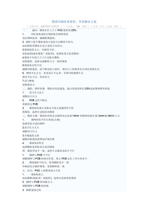
锡膏印刷的重要性:异常解决方案『更新时间:2007-6-6 13:27:37 』『点击数:198 收藏』『作者:佚名| 来源:网络』一.漏印:锡膏未印上大于PAD面积的25%。
1.网孔堵塞或部分锡膏粘在钢网底部清洁钢网底部,减慢脱模速度。
2. 钢网上缺少锡膏或刮刀宽度方向锡膏不均匀。
添加锡膏使锡膏在刮刀宽度方向均匀。
3.锡膏粘度太大,印刷性不好。
添加溶剂(要求锡膏厂商提供),选择粘度合适的锡膏。
4.锡膏中有较大尺寸合金粉末颗粒。
更换锡膏,选择金属颗粒大小一致的锡膏5.锡膏流动性不好减慢印刷速度,适当增加刮刀延时,使刮刀上的锡膏充分填充到网孔里。
6.钢网开孔方式、形状设计不完善,导致印刷脱模不良修改开孔方式、形状设计7.刮刀磨损更换新刮刀二.塌陷:图形坍塌,锡膏向四边塌落,超出焊盘面积的25%造成锡膏图形粘连1. 刮刀压力过大调整刮刀压力2. PCB定位不稳定重新固定PCB3. 锡膏粘度或合金粉末含量太低触变性不好换锡膏,选择合适粘度的锡膏三.锡膏太薄:锡膏的厚度是由钢网决定的0.15mm的钢网控制在0.13mm-0.18mm左右1.钢网厚度不符合要求(太薄)选择厚度合适的钢网2.刮刀压力太大调整刮刀压力3.印刷速度太快减慢印刷速度或增加印刷次数4. 锡膏流动性差选择颗粒度和粘度合适的锡膏四.锡膏厚度不一致:成型不良锡膏表面不平行1. 钢网与PCB不平行调整钢网与PCB的相对位置,效正PCB定位工作台的水平。
2. 锡膏搅拌不均匀,使得颗粒度不一致印刷前充分搅拌锡膏,使得颗粒度一致五.拉尖:PAD上的锡膏成小丘状1.锡膏粘度大添加稀释剂(要求厂商提供),选择合适粘度的锡膏2.钢网与PCB的间隔太大调整钢网与PCB的间隔3.脱模速度过快调整钢网脱模速度4.钢网开孔方式、形状设计不完善,导致印刷脱模不良修改开孔方式、形状设计六.桥连:相邻PAD上的锡膏图形连在一起1.钢网底部不干净有异物清洁钢网底部2.印刷次数多修改机器参数减少印刷次数3.刮刀压力太大调整刮刀压力七.成型模糊:锡膏边缘不平整,表面上有毛刺1.锡膏粘度偏低更换锡膏选择粘度合适的锡膏2.钢网孔壁粗糙钢网验收前用100倍带电源的放大镜检查钢网孔壁的抛光程度3.PAD上的镀层太厚,热风整平不良,产生凹凸不平。
邮件英语 E
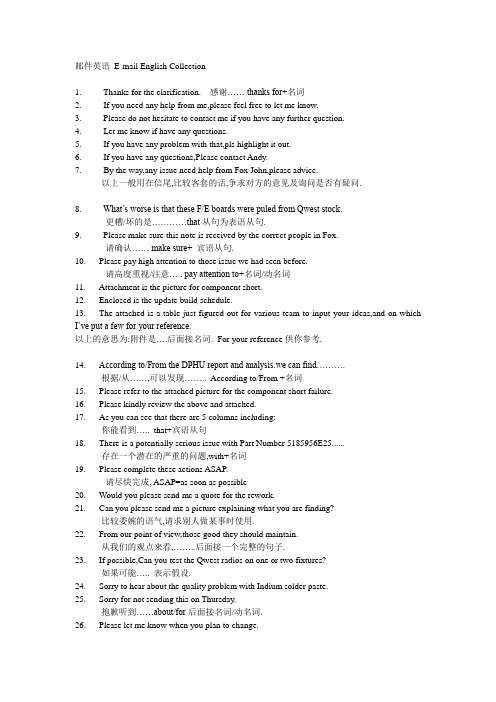
邮件英语E-mail English Collection1. Thanks for the clarification. 感谢…… thanks for+名词2. If you need any help from me,please feel free to let me know.3. Please do not hesitate to contact me if you have any further question.4. Let me know if have any questions.5. If you have any problem with that,pls highlight it out.6. If you have any questions,Please contact Andy.7. By the way,any issue need help from Fox John,please advice.以上一般用在信尾,比较客套的话,争求对方的意见及询问是否有疑问.8. What’s worse is that these F/E boards were puled from Qwest stock.更糟/坏的是…………that从句为表语从句.9. Please make sure this note is received by the correct people in Fox.请确认…… make sure+ 宾语从句.10. Please pay high attention to those issue we had seen before.请高度重视/注意….. pay attention to+名词/动名词11. Attachment is the picture for component short.12. Enclosed is the update build schedule.13. The attached is a table just figured out for various team to input your ideas,and on which I’ve put a few for your reference.以上的意思为:附件是….后面接名词. For your reference供你参考.14. According to/From the DPHU report and analysis.we can find……….根据/从……,可以发现…….. According to/From +名词15. Please refer to the attached picture for the component short failure.16. Please kindly review the above and attached.17. As you can see that there are 5 columns including:你能看到….. that+宾语从句18. There is a potentially serious issue with Part Number 5185956E25......存在一个潜在的严重的问题,with+名词19. Please complete these actions ASAP.请尽快完成, ASAP=as soon as possible20. Would you please send me a quote for the rework.21. Can you please send me a picture explaining what you are finding?比较委婉的语气,请求别人做某事时使用.22. From our point of view,those good they should maintain.从我们的观点来看,……..后面接一个完整的句子.23. If possible,Can you test the Qwest radios on one or two fixtures?如果可能….. 表示假设.24. Sorry to hear about the quality problem with Indium solder paste.25. Sorry for not sending this on Thursday.抱歉听到……about/for后面接名词/动名词.26. Please let me know when you plan to change.27. Would you please let me know the more detail about that?请让我知道…….后面可接宾语从句.28. It would be great if you could provide the spec for these two dimentions.如果….会更好. if引导条件壮语从句.29. The current schedule is very tight./Ibug is in a tight schedule.进度紧一般用Tight.那麼e-mail有什麼寫作要領呢?首先,必須要標題(Heading)欄的“收件人(To)”框中輸入收信人的E-mail 位址。
AuSn (金锡)合金数据表说明书
有关详情: 联系我们的工程师: ****************亚洲 +65 6268 8678 • 中国 +86 (0) 512 628 34900 • 欧洲 +44 (0) 1908 580400 • 美国 +1 315 853 4900所有铟泰公司的焊锡膏和焊片工厂均获得了 IATF 16949:2016 认证。
铟泰公司是 ISO 9001:2015 认证的公司。
本产品说明书仅供参考,并不对所描述的性能做任何担保。
具体质保信息请参见产品合同、发票或者发货单里的文字说明。
除特别说明,铟泰公司的产品和解决方案均市场有售。
©2021铟泰公司物理特性成份Au80/Sn20熔点280°C/536°F 密度14.51克/厘米3抗张强度40,000 psi 剪切强度40,000 psiCTE (热膨胀系数)16 ppm/°C (20°C )导热性0.57w /cm°C (85°C )杨氏模量8.57 x 10⁶ psi所有信息仅供参考,不应被用作所订购产品性能和规格的说明。
AuSn (金锡)的形式铟泰公司的共晶AuSn 焊料有多种形式可选,包括:• 焊锡线• 焊锡带• 焊片• 焊锡膏精密焊锡线、焊锡带或者焊片的尺寸精确,可满足客户的严格要求。
焊锡膏有多种参数的产品来满足特定需求。
焊片还有AuGe 、AuSi 和纯金等可供选择。
表格编号:97800 (SC A4) R5技术支持铟泰公司拥有经验丰富的国际工程师可为我们的客户提供深度技术协助。
技术支持工程师深谙电子和半导体领域中材料科学应用的各个方面,能为焊料属性、合金兼容性和预成型焊片、焊锡线、焊带和焊锡膏的选择提供专家级建议。
铟泰公司的技术支持工程师竭诚为您服务,会第一时间回应所有技术咨询。
安全说明书如欲获取本产品的安全说明书,敬请访问:/sds 。
产品说明书共晶金锡(AuSn )焊料。
锡膏参数差异对比
1.预升温区:室温到150℃,升温速率(1~5)℃/S,但最好不超过3℃/S 2.保温区:150℃~180℃,时间为60S~100S。 3.保温进入回溶区:升温斜率范围在(1-4)℃/S 4.回溶区:最高温度:230℃-255℃,220℃以上时间为30S~90S。 5.冷却区:下降速率一般采用-1℃/S~-4℃/S
对应机型
一般加锡 板使用
20um~ 锡粉粒径 38um
对应机型
20um~ 锡粉粒径 38um
NP08-I+ 锡膏SOP参数设定标准
1.预升温区:采用(1-2)℃的升温速度从室温升温到130℃。 2.保温区:130℃-180℃,保持时间为60S-120S。 3. 保温区进入回焊区:采用(1-2)℃/S的升温斜率。 4. 回焊区:最高温度为235℃-250℃,225℃ 以上的时间应控制在30S-90S。 5. 冷却区,一般采用-1~-4℃/S的斜率降温。
为了便于管控,实际EcoAPP-X100A参 数设置借鉴KOKI锡膏参数进行设置
炉温曲线 炉温曲线 炉温曲线 炉温曲线
对应机型
KOKI温曲线图.p df
粒 径(μm) 20 –pdf
锡粉粒径:20–25mm 目前,我们有两款BOSE产品,分别是 51AC6880002SZ,51AC6880002TZ,使用的 是铟泰锡膏,但是关于回流炉段的产品 SOP上记录的参数,仍是KOKI锡膏的参数 标准,所以需要将其修改为正确的参数。
锡膏料号
锡膏型号
Koki
S3X58-M500-4 33FP00000006
锡膏料号
锡膏型号
33FP0000000Z
indium
锡膏料号
锡膏型号
Pb-Free Solder Fabrications-pds
Solder SpheresIndium Corporation’s unique manufacturing process produces bright and shiny solder spheres supported by Statistical Quality Control systems. Capabilities range from .004” (.10mm) to .095” (2.41mm). All solder spheres can be manufactured utilizing SAC alloys and the higher temperature alloys such as the Au/Sn eutectic solder. Solder spheres can be manufactured for a wide variety of applications from ball-attach to re-balling of BGA’s.Material Safety Data Sheet The MSDS for this product can be found online at /techlibrary/msds.phpTechnical and CustomerSupport Indium Corporation’s internationally experienced engineers provide in-depth technical assistance to our customers. Thoroughly knowledgeable in all facets of Material Science as it applies to the electronics and semiconductor sectors, Technical Support Engineers provide expert advice in solder properties, alloy compatibility and selection of solder preforms, wire, ribbon and paste. Indium Corporation’s Technical Support engineers provide Rapid Response to all technical inquiries, usually within 24 hours.Form No. 97820 R1OVER—>Introduction Indium Corporation can fabricate solders to meet anyapplication. Materials in the table of Pb-Free alloys(see reverse side) can be manufactured into a widerange of products including Solder Wire, Solder Ribbon,Solder Preforms , and Solder Spheres .Solder Wire Manufactured to demanding quality standards,diameter capabilities range from .001” (.025mm) to.250” (6.35mm). In addition, solder wire can bemanufactured to fit all die bonding equipment.Sn/Ag/Cu (SAC) alloys offer the best balance ofproperties for the majority of Pb-Free applications.SAC alloys offer better wetting than the binary eutecticSn/Cu and Sn/Ag. As wetting speed is a key performancerequirement for hand soldering, SAC makes the mostsense for solid or cored solder wire . For lowertemperature rework with the option of controlling theamount of flux, the Bi/Sn/Ag alloy may be the bestchoice. Solid or non-cored wire along with a liquid fluxis the answer when there is too much flux residueassociated with rework. Solder Ribbon Our capabilities allow us to manufacture high quality solder ribbon with a width range of .020” (.5mm) to 3.00” (76mm) and a thickness range of .001” (.025mm) up to as thick as your application requires. Solder ribbon is designed for high-power, high-reliability applications such as microwave devices. For die attach, solder ribbon can be manufactured to comply with all die bonding equipment. This would include Au/Sn and Au/Ge eutectic solders, as they offer a viable solutionfor high temp Pb-Free products.Solder Preforms Solder Preforms can be manufactured in standardshapes such as squares, rectangles, washers, frames, and discs. Typical sizes range from .010” (.254mm) to 2.00” (50.8mm). Smaller and larger sizes, as well as custom shapes are available. A flux coating can also be applied to suite your metallizations. If you are looking to automate, we can put preforms in tape and reel packaging. In addition, solder preforms can be utilized with bulk feeding systems. Solder preforms are viable solution to solder fortification of through-hole components and can eliminate the need for step stencils in pin-in-paste applications. They are also a solution for consistent and precise solder volume in hand soldering.Pb-Free Solder FabricationsThis product data sheet is provided for general information only. It is not intended, and shall not be construed, to warrant or guarantee the performance of the productsdescribed which are sold subject exclusively to written warranties and limitations thereon included in product packaging and invoices.Pb-Free Alloy T ableIndalloy Composition Liquidus Solidus Comments # °C °C 1E52In/48Sn 118 118 Lowest melting point solder that is feasible281 58Bi/42Sn 138 138 Good thermal fatigue performance; established history282 57Bi/42Sn/1Ag 140 139 The addition of Ag adds mechanical strength227 77.2Sn/20In/2.8Ag 187 175 Not for use over 100°C due to In/Sn eutectic @ 118°C254 86.9Sn/10In/3.1Ag 205 204 No In/Sn eutectic problem; potential use for fl ip-chip assembly249 91.8Sn/3.4Ag/4.8Bi 213 211 Board and component metallizations must be Pb-free; Pbcontamination will diminish joint strength241 95.5Sn/3.8Ag/0.7Cu 220 217 Common Pb-free alloy 246 95.5Sn/4Ag/0.5Cu 220 217 Common Pb-free alloy252 95.5Sn/3.9/Ag/0.6Cu 220217 NEMI-promoted alloy (average composition from Indalloy #241and #246)256 96.5Sn/3.0Ag/0.5Cu 220 217 Referred to as the SAC305 alloy121 96.5Sn/3.5Ag 221 221 Binary Sn/Ag eutectic alloy with history of use, marginal wetting244 99.3Sn/0.7Cu 227 227 Inexpensive, possible use in wave soldering133 95Sn/5Sb 240 235 Used in food equipment and refrigeration tubing. Goodwettability and creep resistance209 65Sn/25Ag/10Sb 233 (Melt Point) Die-attach solder, very brittle182 80Au/20Sn 280 280 Excellent mechanical strength and thermal fatigue resistancesolder, used for soldering to Au183 88Au/12Ge 356 356 Close to brazing alloy family, typically used in a reducing atmosphere for step soldering。
Indium8.9HF Overview
1 INDIUM CORPORATION CONFIDENTIAL
Technology Drivers
• High reliability
– Server, telecommunication, automotive
• Miniaturization
– Solution titrated to endpoint and Cl- equivalent is calculated – Only detects ionic halides and many chemicals can cause false positive results
• Ion Chromatography (quantitative)
Validation of Printability: Response to Pause
• Powder Sizes
– Type 3 – Type 4
• Stencil
– 5 mil thickness – Laser-cut – No electropolish
• Aperture Pattern
– At elevated temperatures (such as solder temps) the covalent bonds are broken and halide can react with oxide
Some Ionically Bonded Halides
Some Covalently Bonded Halides
Test Details: 12mil round CSP deposit analyzed; 5-mil laser cut stencil Procedure: Print 12 boards; pause 1-hour; print 12 bATION CONFIDENTIAL
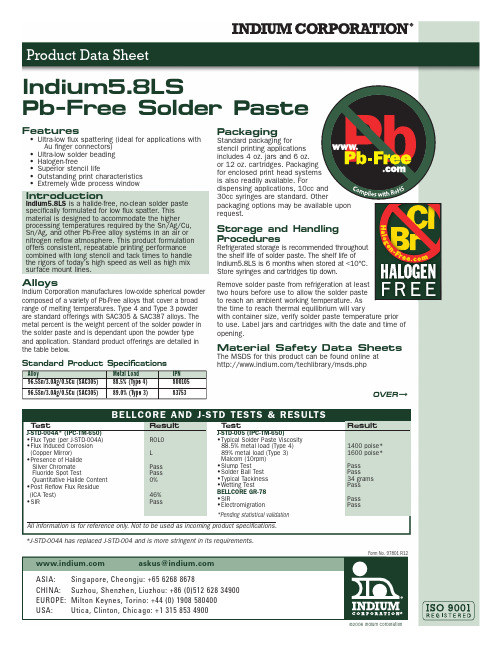
Indium5.8LS Pb-Free Solder Paste 97801 R12
Form No. 97801 R12OVER—>Features• Ultra-low fl ux spattering (ideal for applications withAu fi nger connectors)•Ultra-low solder beading • Halogen-free• Superior stencil life•Outstanding print characteristics•Extremely wide process windowIntroductionIndium5.8LS is a halide-free, no-clean solder paste specifi cally formulated for low fl ux spatter. This material is designed to accommodate the higher processing temperatures required by the Sn/Ag/Cu, Sn/Ag, and other Pb-Free alloy systems in an air or nitrogen refl ow atmosphere. This product formulation offers consistent, repeatable printing performance combined with long stencil and tack times to handle the rigors of today’s high speed as well as high mix surface mount lines.AlloysIndium Corporation manufactures low-oxide spherical powder composed of a variety of Pb-Free alloys that cover a broad range of melting temperatures. Type 4 and Type 3 powder are standard offerings with SAC305 & SAC387 alloys. The metal percent is the weight percent of the solder powder in the solder paste and is dependant upon the powder type and application. Standard product offerings are detailed in the table below.Standard Product Specification sAlloy Metal LoadIPN96.5Sn/3.0Ag/0.5Cu (SAC305) 88.5% (Type 4) 800105 96.5Sn/3.0Ag/0.5Cu (SAC305) 89.0% (Type 3) 83753BELLCORE AND J-STD TESTS & RESULTSIndium5.8LSPb-Free Solder PastePackagingStandard packaging for stencil printing applications includes 4 oz. jars and 6 oz.or 12 oz. cartridges. Packaging is also readily available. Fordispensing applications, 10cc and 30cc syringes are standard. Otherpackaging options may be available upon request.Storage and Handling ProceduresRefrigerated storage is recommended throughout the shelf life of solder paste. The shelf life of Indium5.8LS is 6 months when stored at <10°C. Store syringes and cartridges tip down.Remove solder paste from refrigeration at least two hours before use to allow the solder paste to reach an ambient working temperature. As the time to reach thermal equilibrium will varywith container size, verify solder paste temperature prior to use. Label jars and cartridges with the date and time of opening.Material Safety Data SheetsThe MSDS for this product can be found online at /techlibrary/msds.phpAll information is for reference only. Not to be used as incoming product specifi cations.*J-STD-004A has replaced J-STD-004 and is more stringent in its requirements.T estResult J-STD-004A* (IPC-TM-650)• F lux Type (per J-STD-004A) ROL0• F lux Induced Corrosion (Copper Mirror) L • P resence of Halide Silver Chromate Pass Fluoride Spot Test Pass Quantitative Halide Content 0%• P ost Refl ow Flux Residue (ICA Test) 46%• S IR PassT estResultJ-STD-005 (IPC-TM-650)• T ypical Solder Paste Viscosity 88.5% metal load (Type 4) 1400 poise* 89% metal load (Type 3) 1600 poise* Malcom (10rpm)• S lump Test Pass • S older Ball Test Pass • T ypical Tackiness 34 grams • W etting Test Pass BELLCORE GR-78• S IR Pass • E lectromigration Pass*Pending statistical validation askus@ ASIA:Singapore, Cheongju: +65 6268 8678PrintingStencil Design:Electroformed and laser cut/electropolished stencils produce the best printing characteristics among stencil types. Stencil aperture design is a crucial step in optimizing the print process. The following are a few general recommendations:• Discrete components — A 10-20% reduction of stencil aperture has signifi cantly reduced oreliminated the occurrence of mid-chip solder beads. The “home plate” design is a common method for achieving this reduction.• Fine pitch components — A surface area reduction is recommended for apertures of 20 mil pitch and fi ner. This reduction will help minimize solder balling and bridging that can lead to electrical shorts. Theamount of reduction necessary is process dependent (5-15% is common).• For adequate release of solder paste from stencilaperatures, a minimum aspect ratio of 1.5 is required. The aspect ratio is defi ned as the width of the aperture divided by the thickness of the stencil.Printer Operation:The following are general recommendations for stencil printer optimization. Adjustments may be necessary based on specifi c process requirement:• Solder Paste Bead Size: 20-25mm diameter • Print Speed: 25-100mm/sec• Squeegee Pressure: 0.018-0.027kg/mm of blade length • Underside Stencil Wipe: Once every 10-25 prints • Solder Paste Stencil Life: >8 hrs. @ 30-60% RH & 22°-28°C Cleaning Indium5.8LS is designed for no-clean applications,however the fl ux can be removed if necessary by using acommercially available fl ux residue remover.Stencil Cleaning: This is best performed using isopropyl alcohol (IPA) as a solvent. Most commercially available stencil cleaners work well.Compatible Products• Rework Flux: TACFlux 018Refl owRecommended Profi le:The stated profi le recommendations apply to most Pb-Free alloys in the Sn/Ag/Cu (SAC) alloy system, including SAC 305 (96.5Sn/3.0Ag/0.5Cu). This can be used as a general guideline in establishing a refl ow profi le when using Indium5.8LS Solder Paste. Deviations from these recommendations are acceptable, and may be necessary, based on specifi c process requirements, including board size, thickness & density.Heating Stage:The use of a linear ramp rate or ramp-to-spike (RTS) type profi le assists in minimizing the greatest overall number of defects associated with the refl ow process. If the ramp rate is too fast, it can cause solder balling, solder beading, andaggravated hot slump which can lead to bridging. The ramp rate in the preheat stage of the profi le can range from 0.5°-2.5°C/second (0.5°-1°C/second is ideal). A short soak of20-30 seconds just below the melting point of the solder alloy can help minimize tombstoning when using a RTS type profi le. If necessary, a ramp-soak-spike (RSS) profi le can beimplemented to minimize voiding on BGA and CSP typepackages. A soak zone between 200°-210°C for up to 2 minutes is acceptable.Liquidus Stage:To achieve acceptable wetting and form a quality solder joint, the acceptable temperature range above the melting point of the solder alloy is 12°-50°C (15°-30°C is ideal). The acceptable range for time above liquidus (TAL) is 30-100 seconds (45-60 seconds is ideal). A peak temperature and TAL above these recommendations can result in excessive intermetallic formation that can decrease solder joint reliability.Cooling Stage:A rapid cool down is desired to form a fi ne grain structure. Slow cooling will form a large grain structure, which typically exhibits poor fatigue resistance. The acceptable cooling range is 0.5°C-6.0°C/second (2.0°-6.0°C/second is ideal).This product data sheet is provided for general information only. It is not intended, and shall not be construed, to warrant or guarantee the performance of the products described which are sold subject exclusively to written warranties and limitations thereon included in product packaging and invoices.-Ì>`>À`-> *ÊrÊÓ£Çc/i «i À>ÌÕÀi Êc ®/ iÊ ®ÓxäÓää£xä£ääxäääÊ£ÊÓÊÎÊ{ÊxÊÈÊÇ。
焊锡膏(SOLDER PASTE)的基础知识
1.5 焊锡膏的检验项目 焊锡膏外观
焊料重量百分 比
焊剂酸值测定
焊锡膏的印刷性
焊料成分测定
焊剂卤化物测定
焊 锡 焊锡膏的黏度性试验
焊料粒度分布
焊剂水溶物电导 率测定
膏 使 焊锡膏的塌落度 用
金 焊剂铜镜腐蚀性
属 焊料粉末形状 焊 试验
粉
性 焊锡膏热熔后残渣干燥 粒
剂 焊剂绝缘电阻测
能度
定
焊锡膏的焊球试验
寿命≥6
运送过Biblioteka 焊锡的分辨率B.2.对活性焊
个月
程中元
爬高
2.无刺激性 膏应易清洗
件移位
充分
气味,无毒 掉残留物
害
所需 冰箱
设备
印刷机, 贴片机 再流焊炉 清洗机
模板
显微 镜
焊锡膏润湿性扩展率试 验
1.6 SMT 工艺过程对焊锡膏的技术要求
工艺 焊锡膏 焊锡膏印 贴放元
再流
流程 的存储 刷
件
清洗
检查
性能 要求
1.焊接性能
好,焊点周 1.对免清洗
有一定
焊点
围无飞珠出 焊膏其 SIR
0 度—10
黏结力,
发
良好漏印
现,不腐蚀 应达到 RS≥
度,存放
以免 PCB
亮,
性,良好
元件及 PC 1011Ω
焊锡膏(SOLDER PASTE)的基础知识
1 焊锡膏(SOLDER PASTE)的基础知识 1.1 焊锡膏是将焊料粉末与具有助焊功能的糊状焊剂混合而成的一种浆料,通 常焊料粉末占 90%左右,其余是化学成分. 1.2 我们把能随意改变形态或任意分割的物体称为流体,研究流体受外力而引 起形变与流动行为规律和特征的科学称为流变学.但在工程中则用黏度这一概 念来表征流体黏度性的大小. 1.3 焊锡膏的流变行为 焊锡膏中混有一定量的触变剂,具有假塑性流体性质.(搅拌变稀) 焊锡膏在印刷时,受到刮刀的推力作用,其黏度下降,当到达摸板窗口时,黏度达 到最低,故能顺利通过窗口沉降到 PCB 的焊盘上,随着外力的停止,焊锡膏黏度 又迅速回升,这样就不会出现印刷图形的塌落和漫流,得到良好的印刷效果. 1.4 影响焊锡膏黏度的因素 1.4.1 焊料粉末含量对黏度的影响:焊锡膏中焊料粉末的增加引起黏度的增加. 1.4.2 焊料粉末粒度对黏度的影响:焊料粉末粒度增大时黏度会降低. 1.4.3 温度对焊锡膏黏度的影响:温度升高黏度下降.印刷的最佳环境温度为 2 3+/-3 度. 1.4.4 剪切速率对焊锡膏黏度的影响:剪切速率增加黏度下降.
TP行业常用英文缩写
TP行业常用英文缩写ITO Touch Panel 相关常用术语及专有名词a 尺寸:产品的外形面积b 可视区:透明区,装机后可看到的区域:此区域不能出现不透明的线路及键片等c 驱动面积:实际可操作的区域. 注:驱动面积比可视面积小d 键片:用于粘合上、下线路的双面胶,也可使用粘胶代替e 承托板:粘于下线背面.起支撑产品的作用,由于材料增多,产品透明度有所降低.f 敏感区: 驱动区外形与键片的距离.由于存在键片高度落差,当使用不当,很容易在此区造成ITO 膜断裂导致产品功能不良,在产品设计上尽可能减少落差.此区域虽小但不容忽视g 蚀刻:把多余的ITO 膜用酸腐蚀掉h 预压:用低温把ACF 固定在玻璃上的过程,是为热压前做准备.I 压合:用脉冲热压机利用高温高压力的方式,溶解并固化ACF,最终把FPC 或PET 引出线固定在GLASS 或FILM上J ITO: Indium Tin oxide 氧化铟锡k A TO: Antimony Tin oxide 氧化锑锡l ACF: Anisotropic conductive film 异方性电热融胶带m OCA: optical clear Adhesive 光学透明胶FPC: FLEXIBLE PRINTED CIRCUIT 指可绕性印刷电路板常见缩写PET=Polyester 聚脂薄膜PC=Poly carbonate 聚碳酸脂PP:聚丙烯英文名称:Polypropylene(简称PP)PE:聚乙烯PolyethyleneFPC(B)=Flexible printed circuit(board)柔性印刷线路版ITO=Indium Tin oxide 氧化铟锡OCA=optical clear adhesive 透明胶ACF=anisotropic conductive film 导电热熔胶6.4 专用名词Clear PET:亮面PETanti-glare PET:雾面PETanti-newton ring 防牛顿环anti-reflection 防反射Flat type 平面式Tactile type 触感试Analogy type 类此式Matrix type 矩阵式Capacitance 电容式Top/upper circuit 上线路Adhesive/spacer 粘胶/键片Bottom/lower circuit 下线路rear adhesive 底胶ESD 静电网Full solid shielding 网状静电网Tail 引线Stiffener/trace filler 补强Copper foil铜箔Connector连接器ZIF connector 不打PINNickel-plated 镀镍Gold-plated镀金Aluminium board 铝板Acrylic plate 压克力板(PMMA)Chemically strength tempered glass 强化玻璃Normal glass 普通ITO 玻璃Spacer dot绝缘点Dot pitch 绝缘点点距Heat sealing 热封胶Adhesive paste 粘胶EV A黑色泡棉胶Double tape双面胶Open/short testing 断短路测试Cold solder冷焊Tolerance deviating 容许偏差Insert strip 插条V enting detail 通气槽Costume 外观Release liner 离形纸Fuselage/case 机壳Water-proof frame 防水框Exit trace 出线凹槽Metal dome置弹片Silicone rubber 硅胶Assembly structure and bubble 对折组合结构密合度Bonding 彩色油墨Window hole视窗冲孔Screen ink彩色油墨有关样品规格的专有名词Mechanical characteristics 机械性能1,Tapping durability 敲击寿命2,Pensliding durability 笔画寿命3,Operation force 操作压力4,Impact resistance 耐冲击试验5,Seatic load resistance 耐静压性测试6,Flexible pattern heat seal peeling strength引线拉力测试7, Flexible pattern bending resistance 引线耐弯曲性测试8,Vibration resistance(product)振动测试(产品)9,Package drop 包装跌落测试10,Flexible pattern heat resistance to soldering 引线焊接耐热测试Electric characteristics 电器性能1,Terminal resistance回路电阻2,Insulation resistance 绝缘阻抗3,Linearity线性Appearance 外观1,Dot-like foreign matter 点状杂物2,Linear foreign matter 线状杂物3,Chip and crack 碎裂,破裂4,Seratch 刮伤5,Fisheye on film, Dent on film and air bubble 。
INDIUM CORPORATION ndalloy 18 2 金錫焊膏 产品说明书
china@亞洲:新加坡: +65 6268 8678 接反面—>特點• 在高溫時強度高、熔點高• 抗腐蝕• 與其他貴金屬兼容• 導熱性能優異 簡介Indalloy 182 (80Au/20Sn)的熔點為280°C (556°F)。
它可以做成焊膏的形式,滿足各種具體用途的需要。
金錫焊膏通常用在需要熔點高(超過150°C )、熱疲勞特性好、在高溫下的強度高的情形。
它還用於需要高抗張強度、抗腐蝕的場合,或者在後續的低溫迴流焊製程中焊膏不會熔化的場合。
由於這些原因,Indalloy 182焊膏在軍事、航空航天、醫療等領域得到廣泛應用。
用於Au/Sn 焊膏的助焊劑• RMA-SMQ51AC• NC-SMQ51SC 按照用途和客戶產品使用要求,用於Indalloy 的熱穩定助焊劑有免洗型和RMA 型兩種。
這些助焊劑的產品說網址:techlibrary/pds.php 。
顆粒尺寸Indalloy 182用3號焊粉,這是標準產品。
如果用戶需要,金屬含量從91%到94%,決定於用途和顆粒的尺寸。
針對你的需要,如何確定產品的最適當規格,請與銦泰公司的應用工程師聯絡。
包裝Indalloy 182焊膏有罐裝和注射器包裝的產品。
用於塗佈的標準包裝有10cc 和30cc 的注射器包裝。
如果客戶需可以提供其他包裝的產品。
儲存和搬運方法為了達到最長的保質期,焊I ndalloy 182的保質期與使用的助焊劑有關。
注射器包裝或者筒裝的產品在存放時,防止助焊劑與焊重。
應當讓焊膏的溫度先達到工作環境的溫度,然後才使用。
應當把焊膏從冷藏環境取出來至少4小時之後再使用。
溫度穩定下來所需要的實際時間與包裝的尺寸有關。
在使用之前要檢查焊膏的溫度。
應當在注射器包裝Indalloy 182 金錫焊膏塗佈 是用高速、高可靠性的單點或者多點塗佈自動化設備進行塗佈,但是也可以用手持設備進行塗佈。
使用氣動或者正量裝置可以進行體積精確的塗佈。
- 1、下载文档前请自行甄别文档内容的完整性,平台不提供额外的编辑、内容补充、找答案等附加服务。
- 2、"仅部分预览"的文档,不可在线预览部分如存在完整性等问题,可反馈申请退款(可完整预览的文档不适用该条件!)。
- 3、如文档侵犯您的权益,请联系客服反馈,我们会尽快为您处理(人工客服工作时间:9:00-18:30)。
OVER—>BELLCORE AND J-STD TESTS & RESULTST est Result J-STD-004 (IPC-TM-650)• Flux Type Classifi cation ORL0• Presence of Halide Fluoride Spot Test Pass • Elemental Analysis Halide-Free • Post Refl ow Flux Residue (ICA Test) 0.4% of solder paste • Corrosion Pass • SIR (Post Clean) Pass• Acid Value (Typical) 31.5 T estResult J-STD-005 (IPC-TM-650)• Typical Solder Paste Viscosity(Pb92.5/Sn5/Ag2.5, Type 3, 88%)Brookfi eld (TF 5 rpm)230 kcps Brookfi eld (R7 10 rpm)170 kcps • Slump TestPass • Solder Ball TestPass • Wetting TestPass • Standard Metal Load88%NC-SMQ ®75 Die Attach Solder PastePackagingStandard packaging for dispensing applications includes 25g fi ll and 40g fi ll 10cc, and 100g fi ll 30cc EFD syringes (Semco syringes also available). Other packaging options may be available upon request.Material Safety Data Sheets The MSDS for this product can be found online at /techlibrary/msds.php Features • Ultra-Low Voiding with Minimal Profi ling • Halide-Free • Vacuum Packed, Bubble-Free • Reliable Miss-Free, Clog-Free Dispensing • Consistent Dispensing Deposit Level • Superior Wetting • Compatible with All Common Metal Finishes • Very Low ResidueIntroduction NC-SMQ ®75 is a halide-free, no-clean solder paste formulated to leave a completely benign, invisible residue of 0.4% of paste or <5% of fl ux vehicle. It is designed for refl ow in a nitrogen atmosphere of 100-ppm oxygen or less. This product has superior wetting capabilities compared to most low residue formulations, offers troublefree probe testing and a “no-residue” appearance. NC-SMQ ®75 meets or surpasses all ANSI/J-STD-004, -005 specifi cations and Bellcore Electromigration test criteria.Alloys Indium Corporation manufactures low oxide spherical powder composed of Sn/Pb, Sb/Sn/Pb and Sn/Pb/Ag in a standard Type 3 mesh size. Other non-standard mesh sizes are available upon request. The weight ratio of the solder powder to the solder paste is referred to as the metal load and is typically 88% for standard alloy compositions.Standard Product Specifi catio nsAlloy Metal Content Mesh Size Particle SizeRecommended Needle Size Sn10/Pb88/Ag2 88% Type 3 25 to 45 microns 20 gauge* Sn5/Pb92.5/Ag2.5 (Type 3) Sn5/Pb95 Sn5/Pb85/Sb10Note: (1): 20 gauge needle - 0.58 mm or 0.023 in.All information is for reference only. Not to be used as incoming product specifi cations.Storage and HandlingProceduresRefrigerated storage will prolong the shelf life of solder paste. The shelf life of NC-SMQ®75is 6 months at storage temperatures of -20° to +5°C. When storing solder paste contained in syringes and cartridges, they should be stored tip down. Solder paste should be allowed to reach ambient working temperature prior to use. No heating should be employed.Generally, paste should be removed from refrigeration at least 2 hours before use. Actual time to reach thermal equilibrium will vary with container size. Paste temperature should be verifi ed before use. Cartridges or syringes should be labeled with date and time of opening. DispensingNC-SMQ®75is formulated to be applied using automated high speed, high reliability, single point or multi-point dispensing equipment, but will also function in hand held applications. Highly accurate volumes can be dispensed using either pneumatic or positive displacement devices. Optimal dispensing performance is dependent on storage conditions, equipment type and set up. AtmosphereNC-SMQ®75is designed for use in a nitrogen (100 ppm oxygen or less) atmosphere.Cleaning or Residue Removal The post refl ow residue of NC-SMQ®75can be removed with commercially available solvents. The vehicle is capable of high temperature alloy refl ow without charring but in case of overheating, any charred residue can be removed with the aid of ultrasonic or mechanical agitation.QualityThe Indium Corporation of America is dedicated to producing the highest quality die attach solder paste.NC-SMQ®75is vacuum packaged by highly trained operators under controlled conditions in unique, specially designed equipment to minimize air bubbles in every syringe and cartridge. Rheology and refl ow characteris-tics as well as metal content and identity are carefully confi rmed for each lot. Also, evaluations are performed on each lot to verify dispensing performance.Recommended Profi le:The typical profi le above is designed for use with Sn10/ Pb88/Ag2 or Sn5/Pb92.5/Ag2.5 alloy in a nitrogen atmosphere (100 ppm oxygen or less). It can serve as a general guideline for establishing a profi le for your process and should be regarded as a typical example. Adjustments to this profi le may be necessary based on assembly size, thermal density, and other factors. Use of other alloys with lower or higher liquidus temperatures will also require changes.Heating and Liquidus Stage:Establish a profi le which provides a rapid heating of the assembly to the solder’s liquidus temperature. Ramp rates of 1 to 4°C/sec are recommended, but the nature of the assembly should govern the actual rate. Toachieve acceptable wetting, and to minimize voiding and intermetallics formation, the profi le must include a period of 15 to 30 seconds above the alloy’s liquidus, and a peak temperature of 10 to 20°C above liquidus. However, excessive time above liquidus (and/or excessively high temperatures above liquidus) can produce negative consequences including: charred residue, diffi cult residue removal, excessive intermetallics formation, voiding,and more.Cooling Stage:Cooling after refl ow should be as fast as practical. Thisis desired to form a fi ne-grained metallic structure. Slow cooling will result in a coarse, large grain structure that will exhibit poor thermal cycling and fatigue resistance.This product data sheet is provided for general information only. It is not intended, and shall not be construed, to warrant or guarantee the performance of the products described which are sold subject exclusively to written warranties and limitations thereon included in product packaging and invoices.。
