SBR4060CTFP;SBR4060CT;中文规格书,Datasheet资料
RCLAMP0504F.TCT资料
STOP 3000.000000 MHz
ESD Response (8kV Contact per IEC 61000-4-2)
START. 030 MHz
STOP 3000.000000 MHz
Note: Data is taken with a 10x attenuator
© 2008 Semtech Corp.
tr = 8µs td = 20µs
e-t
td = IPP/2
5
10
15
20
25
30
Time (µs)
Forward Voltage vs. peak Pulse Current
8
7
6
5
4
3
Waveform
2
Parameters:
tr = 8µs
1
td = 20µs
0
0
1
2
3
4
5
6
Peak Pulse Current - IPP (A)
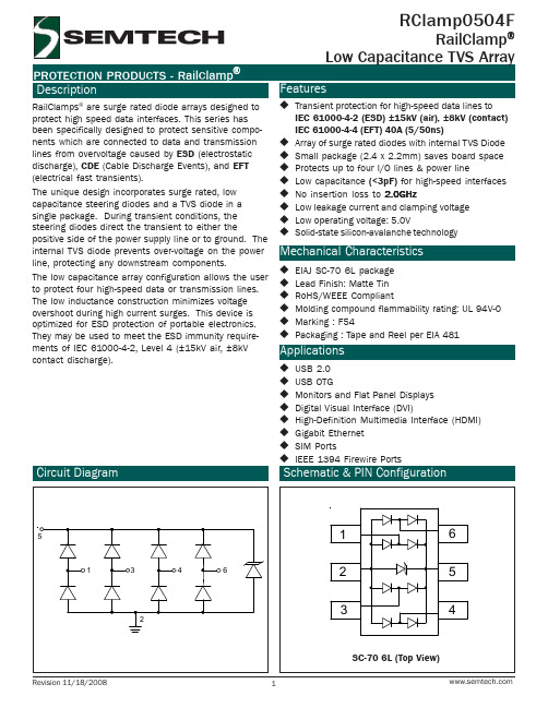
Schematic & PIN Configuration
5
1
3
4
6
2
Revision 11/18/2008
1
1
6
2
5
3
4
SC-70 6L (Top View)
元器件交易网
PROTECTION PRODUCTS Absolute Maximum Rating
0 0
25
50
75
100
125
150
Ambient Temperature - TA (oC)
Clamping Voltage vs. Peak Pulse Current
ACT4060中文资料

ELECTRICAL CHARACTERISTICS
(VIN = 12V, TA = 25°C, unless otherwise specified.)
PARAMETER
Input Voltage Feedback Voltage High-Side Switch On Resistance Low-Side Switch On Resistance SW Leakage Current Limit COMP to Current Limit Transconductance Error Amplifier Transconductance Error Amplifier DC Gain Switching Frequency Short Circuit Switching Frequency Maximum Duty Cycle Minimum Duty Cycle Enable Threshold Voltage Enable Pull-Up Current Supply Current in Shutdown IC Supply Current in Operation Thermal Shutdown Temperature
VALUE
-0.3 to 25 -1 to VIN + 1 VSW - 0.3 to VSW + 8 -0.3 to 6 Internally Limited 105 0.76 -40 to 150 -55 to 150 300
UNIT
V V V V A °C/W W °C °C °C
: Do not exceed these limits to prevent damage to the device. Exposure to absolute maximum rating conditions for long periods may affect device reliability.
MBR4060PT中文资料
Inverters, Free Wheeling, and Polarity Protection Applications · Plastic Material: UL Flammability Classification Rating 94V-0
DS23019 Rev. E-2
1 of 2
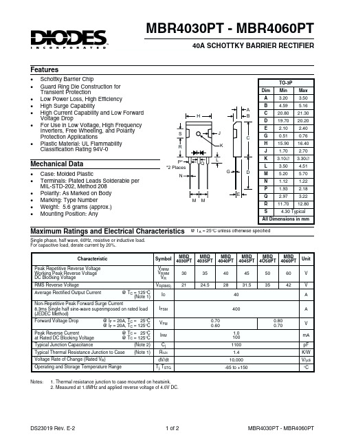
MBR4030PT - MBR4060PT
元器件交易网
50
I(AV), AVERAGE FWD CURRENT (A)
40 30
20
10
0 0
400
50
100
150
TC, CASE TEMPERATURE (°C) Fig. 1 Fwd Current Derating Curve
IR, INSTANTANEOUS REVERSE CURRENT (µA)
DS23019 Rev. E-2
0.1
TC = 75°C
0.01
TC = 25°C
0.001 0
Tj = 25°C
20 40 60 80 100 120 140
PERCENT OF RATED PEAK REVERSE VOLTAGE (%) Fig. 5 Typical Reverse Characteristics
(Note 2)
Typical Thermal Resistance Junction to Case (Note 1)
Voltage Rate of Change (Rated VR)
Operating and Storage Temperature Range
CD74HCT4060M96G4,CD74HCT4060MG4,CD74HCT4060MTG4, 规格书,Datasheet 资料

Data sheet acquired from Harris Semiconductor SCHS207GFeatures•Onboard Oscillator•Common Reset•Negative-Edge Clocking•Fanout (Over Temperature Range)-Standard Outputs. . . . . . . . . . . . . . .10 LSTTL Loads -Bus Driver Outputs . . . . . . . . . . . . .15 LSTTL Loads •Wide Operating Temperature Range . . .-55o C to 125o C •Balanced Propagation Delay and Transition Times •Significant Power Reduction Compared to LSTTL Logic ICs •HC Types-2V to 6V Operation-High Noise Immunity: N IL = 30%, N IH = 30% of V CC at V CC = 5V •HCT Types- 4.5V to 5.5V Operation-Direct LSTTL Input Logic Compatibility,V IL = 0.8V (Max), V IH = 2V (Min)-CMOS Input Compatibility, I l ≤1µA at V OL , V OHDescriptionThe ’HC4060and ’HCT4060each consist of an oscillator section and 14ripple-carry binary counter stages.The oscillator configuration allows design of either RC or crystal oscillator circuits.A Master Reset input is provided which resets the counter to the all-0’s state and disables the oscillator.A high level on the MR line accomplishes the reset function.All counter stages are master-slave flip-flops.The state of the counter is advanced one step in binary order onthe negative transition of φI (and φO).All inputs and outputs are buffered.Schmitt trigger action on the input-pulse-line permits unlimited rise and fall times.In order to achieve a symmetrical waveform in the oscillator section the HCT4060input pulse switch points are the same as in the HC4060;only the MR input in the HCT4060has TTL switching levels.PinoutCD54HC4060, CD54HCT4060 (CERDIP)CD74HC4060 (PDIP, SOIC, TSSOP)CD74HCT4060 (PDIP, SOIC)TOP VIEWOrdering InformationPART NUMBER TEMP. RANGE(o C)PACKAGE CD54HC4060F3A -55 to 12516 Ld CERDIP CD54HCT4060F3A -55 to 12516 Ld CERDIP CD74HC4060E -55 to 12516 Ld PDIP CD74HC4060M -55 to 12516 Ld SOIC CD74HC4060MT -55 to 12516 Ld SOIC CD74HC4060M96-55 to 12516 Ld SOIC CD74HC4060PW -55 to 12516 Ld TSSOP CD74HC4060PWR -55 to 12516 Ld TSSOP CD74HC4060PWT -55 to 12516 Ld TSSOP CD74HCT4060E -55 to 12516 Ld PDIP CD74HCT4060M -55 to 12516 Ld SOIC CD74HCT4060MT -55 to 12516 Ld SOIC CD74HCT4060M96-55 to 12516 Ld SOICNOTE:When ordering,use the entire part number.The suffixes 96and R denote tape and reel.The suffix T denotes a small-quantity reel of 250.14151691312111012345768Q12Q13Q14Q6Q5Q7GND Q4V CC Q8Q9MR φI φO φOQ10February 1998 - Revised October 2003CAUTION: These devices are sensitive to electrostatic discharge. Users should follow proper IC Handling Procedures.CD54HC4060, CD74HC4060,CD54HCT4060, CD74HCT4060High-Speed CMOS Logic14-Stage Binary Counter with Oscillator[ /Title (CD74HC4060,CD74HCT4060)/Sub-ject (High Speed CMOSFunctional DiagramφIQ4Q5Q6Q7Q9Q12Q14φO φOMRQ13Q10Q814-STAGE RIPPLE COUNTER ANDOSCILLATORGND = 8V CC = 1675461313215141211910FIGURE 1.LOGIC BLOCK DIAGRAMTRUTH TABLEøIMR OUTPUT STATE ↑L No Change ↓L Advance to Next State XHAll Outputs are Lowø1Q1FF1ø1Q1Rø4Q4FF4ø4Q4Rø14Q14FF14ø14Q14Rø5Q13FF5 - FF13ø5Q13R7235, 4, 6, 14, 13, 15, 1Q5 - Q10, Q12MR1211109Q14Q13Q4øO øO ø1Absolute Maximum Ratings Thermal InformationDC Supply Voltage, V CC. . . . . . . . . . . . . . . . . . . . . . . .-0.5V to 7V DC Input Diode Current, I IKFor V I < -0.5V or V I > V CC + 0.5V. . . . . . . . . . . . . . . . . . . . . .±20mA DC Output Diode Current, I OKFor V O < -0.5V or V O > V CC + 0.5V . . . . . . . . . . . . . . . . . . . .±20mA DC Drain Current, per Output, I OFor -0.5V < V O < V CC + 0.5V. . . . . . . . . . . . . . . . . . . . . . . . . .±25mA DC V CC or Ground Current, I CC . . . . . . . . . . . . . . . . . . . . . . . . .±50mA Operating ConditionsTemperature Range, T A . . . . . . . . . . . . . . . . . . . . . .-55o C to 125o C Supply Voltage Range, V CCHC T ypes . . . . . . . . . . . . . . . . . . . . . . . . . . . . . . . . . . . . .2V to 6V HCT T ypes . . . . . . . . . . . . . . . . . . . . . . . . . . . . . . . . .4.5V to 5.5V DC Input or Output Voltage, V I, V O . . . . . . . . . . . . . . . . .0V to V CC Input Rise and Fall Time2V . . . . . . . . . . . . . . . . . . . . . . . . . . . . . . . . . . . . . .1000ns (Max) 4.5V. . . . . . . . . . . . . . . . . . . . . . . . . . . . . . . . . . . . . .500ns (Max) 6V . . . . . . . . . . . . . . . . . . . . . . . . . . . . . . . . . . . . . . .400ns (Max)Thermal Resistance (T ypical, Note 1)θJA (o C/W) E (PDIP) Package . . . . . . . . . . . . . . . . . . . . . . . . . .67M (SOIC) Package. . . . . . . . . . . . . . . . . . . . . . . . . .73PW (TSSOP) Package . . . . . . . . . . . . . . . . . . . . . .108 Maximum Junction T emperature. . . . . . . . . . . . . . . . . . . . . . .150o C Maximum Storage Temperature Range . . . . . . . . . .-65o C to 150o C Maximum Lead T emperature (Soldering 10s). . . . . . . . . . . . .300o C (SOIC - Lead Tips Only)CAUTION:Stresses above those listed in“Absolute Maximum Ratings”may cause permanent damage to the device.This is a stress only rating and operation of the device at these or any other conditions above those indicated in the operational sections of this specification is not implied.NOTE:1.The package thermal impedance is calculated in accordance with JESD 51-7.DC Electrical SpecificationsPARAMETER SYMBOLTESTCONDITIONS VCC(V)25o C-40o C TO 85o C-55o C TO125o CUNITS V I(V)I O(mA)MIN TYP MAX MIN MAX MIN MAXHC TYPESHigh Level Input Voltage V IH--2 1.5-- 1.5- 1.5-V4.5 3.15-- 3.15 - 3.15-V6 4.2-- 4.2- 4.2-VLow Level Input Voltage V IL--2--0.5-0.5-0.5V4.5-- 1.35- 1.35- 1.35V6-- 1.8- 1.8- 1.8VHigh Level Output Voltage Q Outputs CMOS Loads V OH V IH or V IL-0.022 1.9-- 1.9- 1.9-V -0.02 4.5 4.4-- 4.4 - 4.4-V-0.026 5.9-- 5.9- 5.9-VHigh Level Output Voltage Q Outputs TTL Loads---------V -4 4.5 3.98-- 3.84- 3.7-V -5.26 5.48-- 5.34- 5.2-VLow Level Output Voltage Q Outputs CMOS Loads V OL V IH or V IL0.022--0.1-0.1-0.1V0.02 4.5--0.1-0.1-0.1V0.026--0.1-0.1-0.1VLow Level Output Voltage Q Outputs TTL Loads---------V4 4.5--0.26-0.33-0.4V5.26--0.26-0.33-0.4VHigh-Level Output VoltageφO Output (Pin 10)CMOS Loads V OH V CC orGND-0.022 1.9-- 1.9- 1.9-V-0.02 4.5 4.4-- 4.4- 4.4-V-0.026 5.9-- 5.9- 5.9-VHigh-Level Output VoltageφO Output (Pin 10)TTL Loads (Note 2)V OH V CC orGND-2.6 4.5 3.98-- 3.84- 3.7-V-3.36 5.48-- 5.34- 5.2-VLow-Level Output VoltageφO Output (Pin 10)CMOS Loads V OL V CC orGND0.022--0.1-0.1-0.1V0.02 4.5--0.1-0.1-0.1V0.026--0.1-0.1-0.1VLow-Level Output VoltageφO Output (Pin 10)TTL Loads V OL V CC orGND2.6 4.5--0.26-0.33-0.4V3.36--0.26-0.33-0.4VHigh-Level Output VoltageφO Output (Pin 9)TTL Loads V OH V IL or V IH-3.2 4.5 3.98-- 3.84- 3.7-V -4.26 5.48-- 5.34- 5.2-VLow-Level Output VoltageφO Output (Pin 9)TTL Loads V OL V IL or V IH-2.6 4.5--0.26-0.33-0.4V -3.36--0.26-0.33-0.4VInput Leakage Current I I V CC orGND-6--±0.1-±1-±1µAQuiescent Device Current I CC V CC orGND06--8-80-160µAHCT TYPESHigh Level Input Voltage V IH-- 4.5 to5.52--2-2-VLow Level Input Voltage V IL-- 4.5 to5.5--0.8-0.8-0.8VHigh Level Output Voltage Q Outputs CMOS Loads V OH V IH or V IL(Note 3)-0.02 4.5 4.4-- 4.4- 4.4-VHigh Level OutputVoltage Q OutputsTTL Loads-4 4.5 3.98-- 3.84- 3.7-VLow Level Output Voltage Q Outputs CMOS Loads V OL V IH or V IL(Note 3)0.02 4.5--0.1-0.1-0.1VLow Level OutputVoltage Q OutputsTTL Loads4 4.5--0.26-0.33-0.4VHigh-Level Output VoltageφO Output (Pin 10)CMOS Loads V OH V CC orGND-0.02 4.5 4.4-- 4.4- 4.4-VHigh-Level Output VoltageφO Output (Pin 10)TTL Loads (Note 2)V OH V CC orGND-2.6 4.5 3.98-- 3.84- 3.7-VLow-Level Output VoltageφO Output (Pin 10)CMOS Loads V OL V CC orGND0.02 4.5--0.1-0.1-0.1VPARAMETER SYMBOLCONDITIONS VCC(V)25o C-40o C TO 85o C-55o C TO125o CUNITS V I(V)I O(mA)MIN TYP MAX MIN MAX MIN MAXLow-Level Output Voltage φO Output (Pin 10)TTL Loads V OLV CC or GND2.64.5--0.26-0.33-0.4VHigh-Level Output Voltage φO Output (Pin 9)TTL Loads V OH V IL or V IH-3.2 4.5 3.98-- 3.84- 3.7-VLow-Level Output Voltage φO Output (Pin 9)TTL Loads V OLV IH or V IL (Note 3)3.24.5-0.26-0.33-0.4VInput Leakage CurrentI IAny Voltage Between V CC and GND - 5.5-±0.1-±1-±1µAQuiescent Device CurrentI CC V CC or GND 0 5.5--8-80-160µA Additional Quiescent Device Current Per Input Pin: 1 Unit Load ∆I CC (Note 4)V CC - 2.1-4.5 to5.5-100360-450-490µANOTES:2.Limits not valid when pin 12 (instead of pin 11) is used as control input.3.For pin 11 V IH = 3.15V, V IL = 0.9V.4.For dual-supply systems theoretical worst case (V I = 2.4V, V CC =5.5V) specification is 1.8mA.PARAMETER SYMBOL CONDITIONSV CC (V)25o C-40o C TO 85o C -55o C TO 125o C UNITS V I (V)I O (mA)MIN TYP MAX MIN MAX MIN MAX HCT Input Loading TableINPUT UNIT LOADSMR0.35NOTE:Unit Load is ∆I CC limit specified in DC Electrical Specifica-tions Table, e.g. 360µA max at 25o C.Prerequisite for Switching SpecificationsPARAMETER SYMBOLV CC (V)25o C-40o C TO 85o C -55o C TO 125o C UNITSMINTYPMAXMINTYPMAXMINTYPMAXHC TYPESMaximum Input Pulse Frequencyf max26--5--4--MHz 4.530--25--20--MHz 635--29--23--MHz Input Pulse Widtht W280--100--120--ns 4.516--20--24--ns 614--17--20--ns Reset Removal Timet REM2100--125--150--ns 4.520--25--30--ns 617--21--26--nsReset Pulse Widtht W280--100--120--ns 4.516--20--24--ns 614--17--20--ns HCT TYPES Maximum Input,Pulse Frequency f max 4.530--25--20--MHz Input Pulse Width t W 4.516--20--24--ns Reset Removal Time t REM 4.526--33--39--ns Reset Pulse Widtht W4.525--31--38--nsPrerequisite for Switching Specifications(Continued)PARAMETER SYMBOLV CC (V)25o C -40o C TO 85o C -55o C TO 125o C UNITS MIN TYP MAX MIN TYP MAX MIN TYP MAX Switching SpecificationsInput t r , t f = 6nsPARAMETERSYMBOLTEST CONDITIONSV CC (V)25o C-40o C TO 85o C -55o C TO 125o C UNITSMINTYPMAXMINMAXMINMAXHC TYPES Propagation Delayt PLH , t PHLC L = 50pF2--300-375-450ns φI to Q44.5--60-75-90ns C L = 15pF 5-25-----ns C L = 50pF6--51-64-78ns Q n to Q n+1t PLH , t PHLC L = 50pF2--80-100-120ns 4.5--16-20-24ns C L = 15pF 5-6-----ns C L = 50pF6--14-17-20ns MR to Q nt PHLC L = 50pF2--175-220-265ns 4.5--35-44-53ns C L = 15pF 5-14-----ns C L = 50pF6--30-37-45ns Output Transition Timet THL , t TLHC L = 50pF2--75-95-110ns 4.5--15-19-22ns 6--13-16-19nsInput Capacitance C I (TBD)Propagation Dissipation Capacitance (Notes 5, 6)C PD---40-----pFHCT TYPES Propagation Delayt PLH , t PHLC L = 50pF2--------ns φI to Q44.5--66-83-100ns C L = 15pF 5-25------ns C L = 50pF6--------nsQ n to Q n+1t PLH , t PHLC L = 50pF2-------ns 4.5--16-20-24ns C L = 15pF 5-6-----ns C L = 50pF6-------ns MR to Q nt PHLC L = 50pF2-------ns 4.5--44-55-66ns C L = 15pF 5-17-----ns C L = 50pF6-------ns Output Transition Timet THL , t TLHC L = 50pF2-------ns 4.5--15-19-22ns 6-------nsInput Capacitance C I (TBD)Propagation Dissipation Capacitance (Notes 5, 6)C PD---40-----pFNOTES:5.C PD is used to determine the dynamic power consumption, per package.6.P D = C PD V CC 2 f i ∑(C L V CC 2 f i /M) where M = 21, 22, 23, ...214, f i =input frequency, C L = output load capacitance.Switching SpecificationsInput t r , t f = 6ns (Continued)PARAMETER SYMBOL TEST CONDITIONS V CC (V)25o C-40o C TO 85o C -55o C TO 125o C UNITS MIN TYP MAX MIN MAX MIN MAX TYPICAL LIMIT VALUES FOR R X AND C XPARAMETER TEST CONDITIONS VOLTAGETYPICAL MAXIMUM LIMITS R X MinimumC X > 1000pF 21K ΩC X > 10pF 4.5C X > 10pF6R X MaximumC X > 10pF 220M ΩC X > 10pF 4.5C X > 10pF6C X MinimumR X > 10K Ω210pFR X > 10K Ω 4.5R X > 10K Ω6R X = 1K Ω21000pF R X = 1K Ω 4.510pF R X = 1K Ω610pF MaximumAstable Oscillator FrequencyC X = 1000pF,R X = 1K Ω20.5MHz (Note 7)C X = 100pF,R X = 1K Ω 4.53MHz (Note 7)C X = 100pF,R X = 1K Ω63MHz (Note 7)NOTE:7.At very high frequencies f =1/2.2R X C X no longer gives an accurate approximation.NOTE:OSC Frequency ≈ 1/2.2 R X C XFor 1M Ω > R X > 1K Ω, C X > 10pF , f < 1MHzFIGURE 2.FREQUENCY OF ON-BOARD OSCILLATOR AS AFUNCTION OF C X AND R X10210110-110-210-310-410-510-110010102103104105106OSCILLATOR FREQUENCY (Hz)C X (µF )T A = 25o C R X = 1K Ω10K Ω100K Ω1M Ω10M ΩCD54/74HC4060, CD54/74HCT4060Typical Performance CurvesNOTE:Outputs should be switching from 10% V CC to 90% V CC in accordance with device truth table.For f MAX ,input duty cycle =50%.FIGURE 3.HC CLOCK PULSE RISE AND FALL TIMES ANDPULSE WIDTHNOTE:Outputs should be switching from 10% V CC to 90% V CC in accordance with device truth table.For f MAX ,input duty cycle =50%.FIGURE 4.HCT CLOCK PULSE RISE AND FALL TIMES ANDPULSE WIDTHFIGURE 5.HC AND HCT TRANSITION TIMES AND PROPAGA-TION DELAY TIMES, COMBINATION LOGIC FIGURE 6.HCT TRANSITION TIMES AND PROPAGATIONDELAY TIMES, COMBINATION LOGICCLOCK90%50%10%GNDV CCt r C L t f C L 50%50%t WLt WH10%t WL + t WH =fC LICLOCK 2.7V 1.3V0.3VGND3Vt r C L = 6nst f C L = 6ns1.3V 1.3V t WLt WH0.3V t WL + t WH =fC L I t PHLt PLHt THL t TLH 90%50%10%50%10%INVERTING OUTPUT INPUTGNDV CCt r = 6nst f = 6ns90%t PHLt PLHt THLt TLH 2.7V 1.3V 0.3V1.3V 10%INVERTING OUTPUTINPUTGND 3Vt r = 6nst f = 6ns90%CD54/74HC4060, CD54/74HCT4060Addendum-Page 1PACKAGING INFORMATIONOrderable Device Status(1)Package Type PackageDrawingPins Package QtyEco Plan(2)Lead/Ball Finish MSL Peak Temp (3)Samples (Requires Login)5962-8768001EA ACTIVE CDIP J 161TBD Call TI Call TI 5962-8977101EA ACTIVE CDIP J 161TBD Call TI Call TICD54HC4060F3A ACTIVE CDIP J 161TBD A42N / A for Pkg Type CD54HCT4060F3A ACTIVE CDIP J 161TBDA42N / A for Pkg TypeCD74HC4060E ACTIVE PDIP N 1625Pb-Free (RoHS)CU NIPDAU N / A for Pkg Type CD74HC4060EE4ACTIVE PDIP N 1625Pb-Free (RoHS)CU NIPDAU N / A for Pkg Type CD74HC4060M ACTIVE SOIC D 1640Green (RoHS & no Sb/Br)CU NIPDAU Level-1-260C-UNLIM CD74HC4060M96ACTIVE SOIC D 162500Green (RoHS & no Sb/Br)CU NIPDAU Level-1-260C-UNLIM CD74HC4060M96E4ACTIVE SOIC D 162500Green (RoHS & no Sb/Br)CU NIPDAU Level-1-260C-UNLIM CD74HC4060M96G4ACTIVE SOIC D 162500Green (RoHS & no Sb/Br)CU NIPDAU Level-1-260C-UNLIM CD74HC4060ME4ACTIVE SOIC D 1640Green (RoHS & no Sb/Br)CU NIPDAU Level-1-260C-UNLIM CD74HC4060MG4ACTIVE SOIC D 1640Green (RoHS & no Sb/Br)CU NIPDAU Level-1-260C-UNLIM CD74HC4060MT ACTIVE SOIC D 16250Green (RoHS & no Sb/Br)CU NIPDAU Level-1-260C-UNLIM CD74HC4060MTE4ACTIVE SOIC D 16250Green (RoHS & no Sb/Br)CU NIPDAU Level-1-260C-UNLIM CD74HC4060MTG4ACTIVE SOIC D 16250Green (RoHS & no Sb/Br)CU NIPDAU Level-1-260C-UNLIM CD74HC4060PW ACTIVE TSSOP PW 1690Green (RoHS & no Sb/Br)CU NIPDAU Level-1-260C-UNLIM CD74HC4060PWE4ACTIVE TSSOP PW 1690Green (RoHS & no Sb/Br)CU NIPDAU Level-1-260C-UNLIM CD74HC4060PWG4ACTIVE TSSOP PW 1690Green (RoHS & no Sb/Br)CU NIPDAU Level-1-260C-UNLIM CD74HC4060PWRACTIVETSSOPPW162000Green (RoHS & no Sb/Br)CU NIPDAU Level-1-260C-UNLIM芯天下--/Addendum-Page 2Orderable Device Status(1)Package Type PackageDrawingPins Package QtyEco Plan(2)Lead/Ball FinishMSL Peak Temp(3)Samples (Requires Login)CD74HC4060PWRE4ACTIVE TSSOP PW 162000Green (RoHS & no Sb/Br)CU NIPDAU Level-1-260C-UNLIM CD74HC4060PWRG4ACTIVE TSSOP PW 162000Green (RoHS & no Sb/Br)CU NIPDAU Level-1-260C-UNLIM CD74HC4060PWT ACTIVE TSSOP PW 16250Green (RoHS & no Sb/Br)CU NIPDAU Level-1-260C-UNLIM CD74HC4060PWTE4ACTIVE TSSOP PW 16250Green (RoHS & no Sb/Br)CU NIPDAU Level-1-260C-UNLIM CD74HC4060PWTG4ACTIVE TSSOP PW 16250Green (RoHS & no Sb/Br)CU NIPDAU Level-1-260C-UNLIM CD74HCT4060E ACTIVE PDIP N 1625Pb-Free (RoHS)CU NIPDAU N / A for Pkg Type CD74HCT4060EE4ACTIVE PDIP N 1625Pb-Free (RoHS)CU NIPDAU N / A for Pkg Type CD74HCT4060M ACTIVE SOIC D 1640Green (RoHS & no Sb/Br)CU NIPDAU Level-1-260C-UNLIM CD74HCT4060M96ACTIVE SOIC D 162500Green (RoHS & no Sb/Br)CU NIPDAU Level-1-260C-UNLIM CD74HCT4060M96E4ACTIVE SOIC D 162500Green (RoHS & no Sb/Br)CU NIPDAU Level-1-260C-UNLIM CD74HCT4060M96G4ACTIVE SOIC D 162500Green (RoHS & no Sb/Br)CU NIPDAU Level-1-260C-UNLIM CD74HCT4060ME4ACTIVE SOIC D 1640Green (RoHS & no Sb/Br)CU NIPDAU Level-1-260C-UNLIM CD74HCT4060MG4ACTIVE SOIC D 1640Green (RoHS & no Sb/Br)CU NIPDAU Level-1-260C-UNLIM CD74HCT4060MT ACTIVE SOIC D 16250Green (RoHS & no Sb/Br)CU NIPDAU Level-1-260C-UNLIM CD74HCT4060MTE4ACTIVE SOIC D 16250Green (RoHS & no Sb/Br)CU NIPDAU Level-1-260C-UNLIM CD74HCT4060MTG4ACTIVESOICD16250Green (RoHS & no Sb/Br)CU NIPDAU Level-1-260C-UNLIM(1)The marketing status values are defined as follows:ACTIVE: Product device recommended for new designs.LIFEBUY: TI has announced that the device will be discontinued, and a lifetime-buy period is in effect.NRND: Not recommended for new designs. Device is in production to support existing customers, but TI does not recommend using this part in a new design.PREVIEW: Device has been announced but is not in production. Samples may or may not be available.OBSOLETE: TI has discontinued the production of the device.芯天下--/PACKAGE OPTION ADDENDUM5-Sep-2011Addendum-Page 3(2)Eco Plan - The planned eco-friendly classification: Pb-Free (RoHS), Pb-Free (RoHS Exempt), or Green (RoHS & no Sb/Br) - please check /productcontent for the latest availability information and additional product content details.TBD: The Pb-Free/Green conversion plan has not been defined.Pb-Free (RoHS): TI's terms "Lead-Free" or "Pb-Free" mean semiconductor products that are compatible with the current RoHS requirements for all 6 substances, including the requirement that lead not exceed 0.1% by weight in homogeneous materials. Where designed to be soldered at high temperatures, TI Pb-Free products are suitable for use in specified lead-free processes.Pb-Free (RoHS Exempt): This component has a RoHS exemption for either 1) lead-based flip-chip solder bumps used between the die and package, or 2) lead-based die adhesive used between the die and leadframe. The component is otherwise considered Pb-Free (RoHS compatible) as defined above.Green (RoHS & no Sb/Br): TI defines "Green" to mean Pb-Free (RoHS compatible), and free of Bromine (Br) and Antimony (Sb) based flame retardants (Br or Sb do not exceed 0.1% by weight in homogeneous material)(3)MSL, Peak Temp. -- The Moisture Sensitivity Level rating according to the JEDEC industry standard classifications, and peak solder temperature.Important Information and Disclaimer:The information provided on this page represents TI's knowledge and belief as of the date that it is provided. TI bases its knowledge and belief on information provided by third parties, and makes no representation or warranty as to the accuracy of such information. Efforts are underway to better integrate information from third parties. TI has taken and continues to take reasonable steps to provide representative and accurate information but may not have conducted destructive testing or chemical analysis on incoming materials and chemicals.TI and TI suppliers consider certain information to be proprietary, and thus CAS numbers and other limited information may not be available for release.In no event shall TI's liability arising out of such information exceed the total purchase price of the TI part(s) at issue in this document sold by TI to Customer on an annual basis.OTHER QUALIFIED VERSIONS OF CD54HC4060, CD54HCT4060, CD74HC4060, CD74HCT4060 :•Catalog: CD74HC4060, CD74HCT4060•Military: CD54HC4060, CD54HCT4060NOTE: Qualified Version Definitions:•Catalog - TI's standard catalog product•Military - QML certified for Military and Defense Applications芯天下--/TAPE AND REELINFORMATION*All dimensionsare nominalDevicePackage Type Package Drawing Pins SPQReel Diameter (mm)Reel Width W1(mm)A0(mm)B0(mm)K0(mm)P1(mm)W (mm)Pin1Quadrant CD74HC4060M96SOIC D 162500330.016.4 6.510.3 2.18.016.0Q1CD74HC4060PWR TSSOP PW 162000330.012.4 6.9 5.6 1.68.012.0Q1CD74HC4060PWT TSSOP PW 16250330.012.4 6.9 5.6 1.68.012.0Q1CD74HCT4060M96SOICD162500330.016.46.510.32.18.016.0Q114-Jul-2012*All dimensionsare nominalDevice Package TypePackage DrawingPins SPQ Length (mm)Width (mm)Height (mm)CD74HC4060M96SOIC D 162500333.2345.928.6CD74HC4060PWR TSSOP PW 162000367.0367.035.0CD74HC4060PWT TSSOP PW 16250367.0367.035.0CD74HCT4060M96SOICD162500333.2345.928.614-Jul-2012IMPORTANT NOTICETexas Instruments Incorporated and its subsidiaries(TI)reserve the right to make corrections,enhancements,improvements and other changes to its semiconductor products and services per JESD46C and to discontinue any product or service per JESD48B.Buyers should obtain the latest relevant information before placing orders and should verify that such information is current and complete.All semiconductor products(also referred to herein as“components”)are sold subject to TI’s terms and conditions of sale supplied at the time of order acknowledgment.TI warrants performance of its components to the specifications applicable at the time of sale,in accordance with the warranty in TI’s terms and conditions of sale of semiconductor products.Testing and other quality control techniques are used to the extent TI deems necessary to support this warranty.Except where mandated by applicable law,testing of all parameters of each component is not necessarily performed.TI assumes no liability for applications assistance or the design of Buyers’products.Buyers are responsible for their products and applications using TI components.To minimize the risks associated with Buyers’products and applications,Buyers should provide adequate design and operating safeguards.TI does not warrant or represent that any license,either express or implied,is granted under any patent right,copyright,mask work right,or other intellectual property right relating to any combination,machine,or process in which TI components or services are rmation published by TI regarding third-party products or services does not constitute a license to use such products or services or a warranty or endorsement e of such information may require a license from a third party under the patents or other intellectual property of the third party,or a license from TI under the patents or other intellectual property of TI.Reproduction of significant portions of TI information in TI data books or data sheets is permissible only if reproduction is without alteration and is accompanied by all associated warranties,conditions,limitations,and notices.TI is not responsible or liable for such altered rmation of third parties may be subject to additional restrictions.Resale of TI components or services with statements different from or beyond the parameters stated by TI for that component or service voids all express and any implied warranties for the associated TI component or service and is an unfair and deceptive business practice. TI is not responsible or liable for any such statements.Buyer acknowledges and agrees that it is solely responsible for compliance with all legal,regulatory and safety-related requirements concerning its products,and any use of TI components in its applications,notwithstanding any applications-related information or support that may be provided by TI.Buyer represents and agrees that it has all the necessary expertise to create and implement safeguards which anticipate dangerous consequences of failures,monitor failures and their consequences,lessen the likelihood of failures that might cause harm and take appropriate remedial actions.Buyer will fully indemnify TI and its representatives against any damages arising out of the use of any TI components in safety-critical applications.In some cases,TI components may be promoted specifically to facilitate safety-related applications.With such components,TI’s goal is to help enable customers to design and create their own end-product solutions that meet applicable functional safety standards and requirements.Nonetheless,such components are subject to these terms.No TI components are authorized for use in FDA Class III(or similar life-critical medical equipment)unless authorized officers of the parties have executed a special agreement specifically governing such use.Only those TI components which TI has specifically designated as military grade or“enhanced plastic”are designed and intended for use in military/aerospace applications or environments.Buyer acknowledges and agrees that any military or aerospace use of TI components which have not been so designated is solely at the Buyer's risk,and that Buyer is solely responsible for compliance with all legal and regulatory requirements in connection with such use.TI has specifically designated certain components which meet ISO/TS16949requirements,mainly for automotive ponents which have not been so designated are neither designed nor intended for automotive use;and TI will not be responsible for any failure of such components to meet such requirements.Products ApplicationsAudio /audio Automotive and Transportation /automotiveAmplifiers Communications and Telecom /communicationsData Converters Computers and Peripherals /computersDLP®Products Consumer Electronics /consumer-appsDSP Energy and Lighting /energyClocks and Timers /clocks Industrial /industrialInterface Medical /medicalLogic Security /securityPower Mgmt Space,Avionics and Defense /space-avionics-defense Microcontrollers Video and Imaging /videoRFID OMAP Mobile Processors /omap TI E2E Community Wireless Connectivity /wirelessconnectivityMailing Address:Texas Instruments,Post Office Box655303,Dallas,Texas75265Copyright©2012,Texas Instruments Incorporated。
SBR20A300CTB;SBR20A300CT;SBR20A300CTFP;中文规格书,Datasheet资料
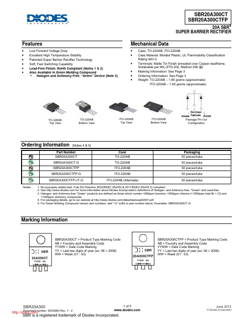
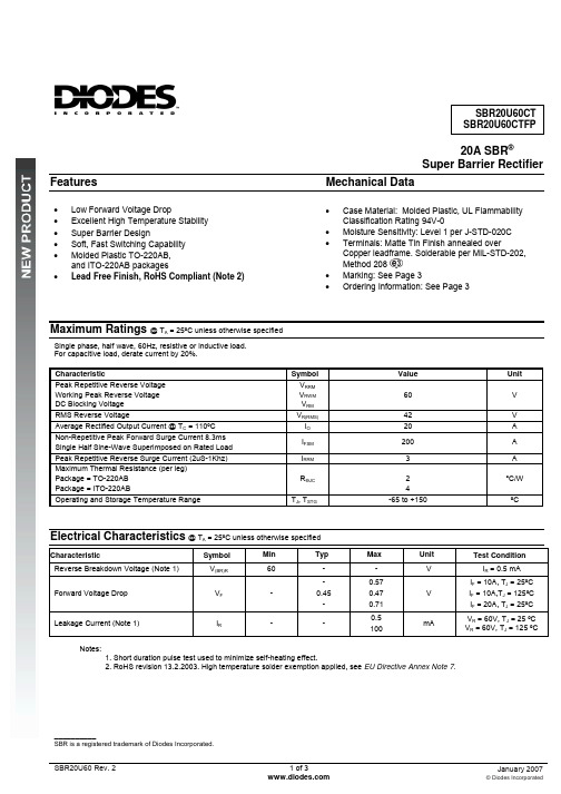
20A SBRSUPER BARRIER RECTIFIERFeatures• Low Forward Voltage Drop• Excellent High Temperature Stability• Patented Super Barrier Rectifier Technology • Soft, Fast Switching Capability• Lead-Free Finish; RoHS Compliant (Notes 1 & 2) •Also Available in Green Molding CompoundHalogen and Antimony Free. “Green” Device (Note 3)Mechanical Data• Case: TO-220AB, ITO-220AB• Case Material: Molded Plastic, UL Flammability Classification Rating 94V-0• Terminals: Matte Tin Finish annealed over Copper leadframe.Solderable per MIL-STD-202, Method 208 • Marking Information: See Page 3 • Ordering Information: See Page 3• Weight: TO-220AB – 1.85 grams (approximate)ITO-220AB – 1.65 grams (approximate)Ordering Information (Notes 4 & 5)Part Number Case PackagingPbSBR20A300CT TO-220AB 50 pieces/tube GreenSBR20A300CT-G TO-220AB 50pieces/tube PbSBR20A300CTFP ITO-220AB 50 pieces/tube GreenSBR20A300CTFP-G ITO-220AB 50pieces/tube GreenSBR20A300CTFP-JT-GITO-220AB (Alternate)50 pieces/tubeNotes:1. No purposely added lead. Fully EU Directive 2002/95/EC (RoHS) & 2011/65/EU (RoHS 2) compliant.2. See for more information about Diodes Incorporated’s definitions of Halogen- and Antimony-free, "Green" and Lead-free.3. Halogen- and Antimony-free "Green” products are defined as those which contain <900ppm bromine, <900ppm chlorine (<1500ppm total Br + Cl) and <1000ppm antimony compounds.4. For packaging details, go to our website at /datasheets/ap02007.pdf.5. For Green Molding Compound version part numbers, add "-G" suffix to part number above. Examples: SBR20A300CT-G.Marking InformationPackage Pin Out ConfigurationTO-220AB Top ViewITO-220AB Top ViewTO-220AB Bottom ViewITO-220AB Bottom ViewSBR20A300CTFP = Product Type Marking Code AB = Foundry and Assembly Code YYWW = Date Code MarkingYY = Last two digits of year (ex: 06 = 2006) WW = Week (01 - 53)SBR20A300CT = Product Type Marking Code AB = Foundry and Assembly Code YYWW = Date Code MarkingYY = Last two digits of year (ex: 06 = 2006) WW = Week (01 - 53)Maximum Ratings (Per Leg) @T A = 25°C unless otherwise specifiedSingle phase, half wave, 60Hz, resistive or inductive load. For capacitance load, derate current by 20%.Characteristic Symbol Value UnitPeak Repetitive Reverse VoltageWorking Peak Reverse Voltage DC Blocking Voltage V RRM V RWM V RM 300 V Average Rectified Output Current (Per Leg) (Total) I O1020 A Non-Repetitive Peak Forward Surge Current 8.3msSingle Half Sine-Wave Superimposed on Rated Load I FSM180 A Peak Repetitive Reverse Surge Current (2uS-1Khz) I RRM 3 A Isolation Voltage (ITO-220AB Only)From terminal to heatsink t = 3 sec. V AC2000 VThermal Characteristics (Per Leg)Characteristic Symbol Value UnitTypical Thermal ResistancePackage = TO-220AB Package = ITO-220ABR θJC 24ºC/W Operating and Storage Temperature Range T J , T STG -65 to +175 ºCElectrical Characteristics (Per Leg) @T A = 25°C unless otherwise specifiedCharacteristic Symbol Min Typ Max Unit Test ConditionForward Voltage Drop V F- - 0.70 - 0.920.78 1.06 V I F = 10A, T J = 25ºC I F = 10A, T J = 125ºC I F = 20A, T J = 25ºCLeakage Current (Note 6) I R- - 0.110 mA V R = 300V, T J = 25ºC V R = 300V, T J = 125ºCReverse Recovery Time t rr - 25 30 ns I F = 0.5A, I R = 1A, I RR = 0.25A- 28 35I F = 1A, V R = 30Vdi/dt = 100A/μs, T J = 25ºCNotes: 6. Short duration pulse test used to minimize self-heating effect. 7. Using heatsink (by black Aluminum 45mm * 20mm * 12mm)Fig. 1 Forward Power DissipationI , AVERAGE FORWARD CURRENT (A)F(AV)P , P O W E R D I S S I P A T I O N (W )DV , INSTANTANEOUS FORWARD VOLTAGE (mV)Fig. 2 Typical Forward Characteristics F 100I , I N S T A N T A N E O U S F O R W A R D C U R R E N T (A )FI , I N S T A N T A N E O U S R E V E R S E C U R R E N T (µA )R Fig. 3 Typical Reverse CharacteristicsV , INSTANTANEOUS REVERSE VOLTAGE (V)R Fig. 4 Forward Current Derating Curve2468T , AMBIENT TEMPERATURE (C)A °I , A V E R A G E F OR W A R D C U R R E N T (A )F (A V )Fig. 5 Operating T emperature DeratingV , DC REVERSE VOLTAGE (V)R T ,D E R A T E D A M B I E N T T E M P E R A T U R E (C )A °Package Outline DimensionsITO-220ABDim Min Typ MaxA 4.50 4.70 4.90A1 3.04 3.24 3.44A2 2.56 2.76 2.96b 0.500.600.75b1 1.10 1.20 1.35c 0.500.600.70D 15.6715.8716.07D1 8.999.199.39e 2.54E 9.9110.1110.31L 9.459.7510.05L1 15.8016.0016.20P 2.98 3.18 3.38Q 3.10 3.30 3.50All Dimensions in mm TO-220ABDim Min Typ MaxA 3.56- 4.82A1 0.51- 1.39A2 2.04- 2.92b 0.390.81 1.01b2 1.15 1.24 1.77c 0.356- 0.61D 14.22- 16.51D1 8.39- 9.01e 2.54e1 5.08E 9.66- 10.66H1 5.85- 6.85L 12.70- 14.73L1 - - 6.35P 3.54- 4.08Q 2.54- 3.42All Dimensions in mmITO220ABDim Min MaxA 4.36 4.77A1 2.54 3.10A2 2.54 2.80b 0.55 0.75b1 1.20 1.50c 0.38 0.68D 14.5015.50D1 8.38 8.89e 2.41 2.67E 9.72 10.27L 9.87 10.67L1 15.8 17.00P 3.08 3.39Q 2.60 3.00All Dimensions in mmPIMPORTANT NOTICEDIODES INCORPORATED MAKES NO WARRANTY OF ANY KIND, EXPRESS OR IMPLIED, WITH REGARDS TO THIS DOCUMENT, INCLUDING, BUT NOT LIMITED TO, THE IMPLIED WARRANTIES OF MERCHANTABILITY AND FITNESS FOR A PARTICULAR PURPOSE (AND THEIR EQUIVALENTS UNDER THE LAWS OF ANY JURISDICTION).Diodes Incorporated and its subsidiaries reserve the right to make modifications, enhancements, improvements, corrections or other changes without further notice to this document and any product described herein. Diodes Incorporated does not assume any liability arising out of the application or use of this document or any product described herein; neither does Diodes Incorporated convey any license under its patent or trademark rights, nor the rights of others. Any Customer or user of this document or products described herein in such applications shall assume all risks of such use and will agree to hold Diodes Incorporated and all the companies whose products are represented on Diodes Incorporated website, harmless against all damages.Diodes Incorporated does not warrant or accept any liability whatsoever in respect of any products purchased through unauthorized sales channel. Should Customers purchase or use Diodes Incorporated products for any unintended or unauthorized application, Customers shall indemnify and hold Diodes Incorporated and its representatives harmless against all claims, damages, expenses, and attorney fees arising out of, directly or indirectly, any claim of personal injury or death associated with such unintended or unauthorized application.Products described herein may be covered by one or more United States, international or foreign patents pending. Product names and markings noted herein may also be covered by one or more United States, international or foreign trademarks.LIFE SUPPORTDiodes Incorporated products are specifically not authorized for use as critical components in life support devices or systems without the express written approval of the Chief Executive Officer of Diodes Incorporated. As used herein:A. Life support devices or systems are devices or systems which:1. are intended to implant into the body, or2. support or sustain life and whose failure to perform when properly used in accordance with instructions for use provided in thelabeling can be reasonably expected to result in significant injury to the user.B. A critical component is any component in a life support device or system whose failure to perform can be reasonably expected to cause thefailure of the life support device or to affect its safety or effectiveness.Customers represent that they have all necessary expertise in the safety and regulatory ramifications of their life support devices or systems, and acknowledge and agree that they are solely responsible for all legal, regulatory and safety-related requirements concerning their products and any use of Diodes Incorporated products in such safety-critical, life support devices or systems, notwithstanding any devices- or systems-related information or support that may be provided by Diodes Incorporated. Further, Customers must fully indemnify Diodes Incorporated and its representatives against any damages arising out of the use of Diodes Incorporated products in such safety-critical, life support devices or systems.Copyright © 2012, Diodes Incorporated分销商库存信息:DIODESSBR20A300CTB SBR20A300CT SBR20A300CTFP。
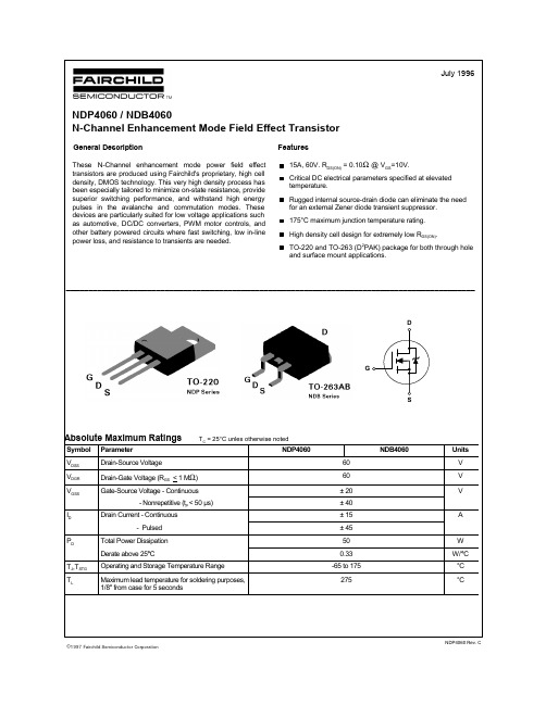
NDP4060中文资料
ON CHARACTERISTICS (Note 1) Gate Threshold Voltage 4 3.6 0.1 0.165 A S V
Ω
DYNAMIC CHARACTERISTICS Input Capacitance Output Capacitance Reverse Transfer Capacitance 370 165 50 450 200 100 pF pF pF
SWITCHING CHARACTERISTICS (Note 1) Turn - On Delay Time Turn - On Rise Time Turn - Off Delay Time Turn - Off Fall Time Total Gate Charge Gate-Source Charge Gate-Drain Charge VDS = 48 V ID = 15 A, VGS = 10 V VDD = 30 V, ID = 15 A VGS = 10 V, RGEN = 25 Ω 8 70 18 37 12.7 3.2 7 20 100 30 50 17 ns ns ns ns nC nC nC
SBR20U60CT中文资料
20A SBR®Super Barrier RectifierFeatures MechanicalData• Case Material: Molded Plastic, UL FlammabilityClassification Rating 94V-0• Moisture Sensitivity: Level 1 per J-STD-020C• Terminals: Matte Tin Finish annealed overCopper leadframe. Solderable per MIL-STD-202,Method 208• Marking: See Page 3• Ordering Information: See Page 3• Low Forward Voltage Drop• Excellent High Temperature Stability• Super Barrier Design• Soft, Fast Switching Capability• Molded Plastic TO-220AB,and ITO-220AB packages• Lead Free Finish, RoHS Compliant (Note 2)Maximum Ratings @ T A = 25ºC unless otherwise specifiedSingle phase, half wave, 60Hz, resistive or inductive load.For capacitive load, derate current by 20%.Characteristic SymbolValueUnit Peak Repetitive Reverse VoltageWorking Peak Reverse VoltageDC Blocking VoltageV RRMV RWMV RM60 VRMS Reverse Voltage V R(RMS)42 VAverage Rectified Output Current @ T C = 110ºC I O20 ANon-Repetitive Peak Forward Surge Current 8.3msSingle Half Sine-Wave Superimposed on Rated LoadI FSM200 APeak Repetitive Reverse Surge Current (2uS-1Khz) I RRM 3 AMaximum Thermal Resistance (per leg)Package = TO-220ABPackage = ITO-220ABRӨJC 24°C/WOperating and Storage Temperature Range T J, T STG-65 to +150 ºCElectrical Characteristics@ T A = 25ºC unless otherwise specifiedCharacteristic SymbolMin Typ Max Unit Test ConditionReverse Breakdown Voltage (Note 1) V(BR)R60 - - V I R = 0.5 mAForward Voltage Drop V F--0.45-0.570.470.71VI F = 10A, T J = 25ºCI F = 10A,T J = 125ºCI F = 20A, T J = 25ºCLeakage Current (Note 1) I R- -0.5100mAV R = 60V, T J= 25 ºCV R = 60V, T J = 125 ºCNotes:1. Short duration pulse test used to minimize self-heating effect.2. RoHS revision 13.2.2003. High temperature solder exemption applied, see EU Directive Annex Note 7.__________SBR is a registered trademark of Diodes Incorporated.Package Outline DrawingsTO-220ABITO-220ABTO-220ABDIM. MIN. MAX.A 4.47 4.67 b 0.71 0.91 b1 1.17 1.37 c 0.31 0.53 D 14.65 15.35 D1 8.50 8.90 E 10.01 10.31 e 2.54 typ e1 4.98 5.18 F 1.17 1.37 J1 2.52 2.82 L 13.40 13.80 L1 3.56 3.96 ØP 3.735 3.935 Q 2.59 2.89All Dimensions in MillimetersITO-220ABDIM. MIN. MAX.A 4.30 4.70b 0.50 0.75 b1 1.10 1.35 b2 1.50 1.75c 0.50 0.75 D 14.80 15.20 E 9.96 10.36 e 2.54 typ F 2.80 3.20 J1 2.50 2.90 L 12.80 13.60 L1 1.70 1.90 ØP 3.50 typ Q 2.70 typAll Dimensions in MillimetersMarking, Polarity, Weight & Ordering InformationSBR20U60CT SBR20U60CTFP Case StyleTO-220AB ITO-220ABtAnodeCommonCathode AnodePolarityCasetAnodeCommonCathode AnodeMarking2.1g 1.9gWeightOrderingInformationSBR20U60CT SBR20U60CTFP50 pieces/tube50 pieces/tubeYY = Last two digits of year, ex = 06 = 2006Date CodeWW = Week (01-52)Other MarkingInformationA = Foundry CodeB = Assembly CodeIMPORTANT NOTICEDiodes Incorporated and its subsidiaries reserve the right to make modifications, enhancements, improvements, corrections or other changeswithout further notice to any product herein. Diodes Incorporated does not assume any liability arising out of the application or use of any productdescribed herein; neither does it convey any license under its patent rights, nor the rights of others. The user of products in such applications shallassume all risks of such use and will agree to hold Diodes Incorporated and all the companies whose products are represented on our website,harmless against all damages.LIFE SUPPORTDiodes Incorporated products are not authorized for use as critical components in life support devices or systems without the expressed writtenapproval of the President of Diodes Incorporated.。
4060窑参数(精)

第八章技术规格和图纸1 招标设备清单1.1 标书编号:CHMC-09ZB15028-01-041.2 设备名称:回转窑1.3 数量:一套1.4 交货期:合同生效之日起11个月,交至项目现场。
2 详细技术要求:回转窑3 设备需求一览表4供货范围注:窑主减速机要求强制润滑,其润滑油站业主单独订货,供货商必须提出其详细技术参数供业主采购参考。
5主要技术性能参数要求(用于锻烧水泥熟料)5.1回转窑同时要求:1、三挡支撑瓦的测温点要求2支/块瓦,一个测油温度,一个测瓦温度;2、液压挡轮的三套轴承采用SKF轴承,并增加一个PT100测温点,轴承润滑采用手动干油泵润滑,油泵型号为型号:SGZ-8工作压力:7MPa 容积:8kg,挡轮液压油站由业主自行采购,供货商必须提出其详细技术参数供业主采购参考。
4、主电机选用上海南洋电机厂产品,轴承选用SKF轴承;5、随机备件清单:窑头护板2块,窑尾护板2块,窑头护板螺栓、螺母3套,窑尾护板螺栓、螺母3套。
5.2 技术要求5.2.1机械规范5.2.1.1制造样图中未注明的技术要求按JC333-91标准执行。
5.2.1.2机械加工部位线性尺寸的未注公差按GB/T1804-m级。
5.2.1.2窑筒体开检修口必须采用冷加工,检修口周围必须100%进行超声波探伤。
5.2.1.3制造中焊接件应符合建材机械焊接的有关规定。
5.2.1.4铸钢件应符合JC401.1-401.4的有关规定。
5.2.2电气规范5.2.2.1为了适应水泥厂的实际情况及对电器控制的要求,电气控制箱的控制应采用A-B小型的PLC(可编程序控制器)的控制,以确保设备的可靠运行。
控制电源220VAC,主传动电机直流调速。
5.2.2.2控制箱应具有两种控制方式集中控制由中央控制计算机(DCS)进行远程控制。
机旁控制在控制箱上可单机开停每台设备(如电机、加热器等),也可以按程序以机旁自动方式开停设备5.2.2.3控制箱应能输入的信号DCS驱动接通启动,断开停止。
SBR30A40CT;SBR30A40CTFP;中文规格书,Datasheet资料

SBR is a registered trademark of Diodes Incorporated.30A SBRSUPER BARRIER RECTIFIERFeatures• Low Forward Voltage Drop• Excellent High Temperature Stability• Patented Super Barrier Rectifier Technology • Soft, Fast Switching Capability• Lead Free Finish, RoHS Compliant (Note 1)• Also Available in Green Molding Compound (Note 2)Mechanical Data• Case: TO-220AB, ITO-220AB• Case Material: Molded Plastic, UL Flammability Classification Rating 94V-0• Terminals: Matte Tin Finish annealed over Copper leadframe.Solderable per MIL-STD-202, Method 208 • Weight: TO-220AB – 1.85 grams (approximate)ITO-220AB – 1.65 grams (approximate)Ordering Information (Notes 2 and 3)Part Number Case PackagingSBR30A40CT TO-220AB 50 pieces/tube SBR30A40CT-G TO-220AB50 pieces/tube SBR30A40CTFP ITO-220AB 50pieces/tube SBR30A40CTFP-G ITO-220AB 50 pieces/tube SBR30A40CTFP-JT ITO-220AB (Alternate)50 pieces/tubeNotes: 1. EU Directive 2002/95/EC (RoHS). All applicable RoHS exemptions applied, see EU Directive 2002/95/EC Annex Notes . 2. For Green Molding Compound version part numbers, add "-G" suffix to part number above. Examples: SBR30A40CT-G. 3. For packaging details, go to our website at .Marking InformationTO-220AB Top View ITO-220AB Top View Package Pin Out ConfigurationTO-220AB Bottom View ITO-220AB Bottom ViewSBR30A40CTFP = Product Type Marking Code AB = Foundry and Assembly Code YYWW = Date Code MarkingYY = Last two digits of year (ex: 06 = 2006) WW = Week (01-52)SBR30A40CT = Product Type Marking Code AB = Foundry and Assembly Code YYWW = Date Code MarkingYY = Last two digits of year (ex: 06 = 2006) WW = Week (01-52)SBR is a registered trademark of Diodes Incorporated.Maximum Ratings @T A = 25°C unless otherwise specifiedSingle phase, half wave, 60Hz, resistive or inductive load. For capacitance load, derate current by 20%.Characteristic Symbol Value Unit Peak Repetitive Reverse VoltageWorking Peak Reverse Voltage DC Blocking VoltageV RRM V RWM V RM 40 VAverage Rectified Output Current @ T C = 110ºC I O 30 ANon-Repetitive Peak Forward Surge Current 8.3ms Single Half Sine-Wave Superimposed on Rated Load I FSM 250 APeak Repetitive Reverse Surge Current (2uS-1Khz) I RRM 3 AIsolation Voltage (ITO-220AB Only) From terminal to heatsink t = 3 sec. V AC2000 VThermal CharacteristicsCharacteristic Symbol Value UnitTypical Thermal Resistance (per leg)Package = TO-220AB Package = ITO-220ABR θJC2 4 ºC/W Operating and Storage Temperature Range T J , T STG-65 to +150ºCElectrical Characteristics @T A = 25°C unless otherwise specifiedCharacteristicSymbol Min Typ Max UnitTest ConditionForward Voltage Drop V F -- 0.420.50 0.45V I F = 15A, T J = 25ºC I F = 15A, T J= 125ºC Leakage Current (Note 4)I R- -0.5100mAV R = 40V, T J = 25ºC V R = 40V, T J = 125ºCNotes: 4. Short duration pulse test used to minimize self-heating effect.255075100125150T C CASE TEMPERATURE (°C)I F (A V E ), A V E R A G E F O R W A R D C U R R E N T (A )Figure 1: Current Derating Curve, Per ElementSBR is a registered trademark of Diodes Incorporated.V , INSTANTANEOUS FORWARD VOLTAGE (mV)Fig. 2 F Typical Forward CharacteristicsV , INSTANTANEOUS REVERSE VOLTAGE (V)Fig. 3 Typical Reverse CharacteristicsR I , I N S T A N T A N E O U S R E V E R S E C U R R E N T (µA )RPackage Outline DimensionsNotes:5. For product manufactured with Date Code 0733 (week 33, 2007) and newer, please refer to ITO-220AB dimensions. For product manufactured prior to Date Code 0733, please refer to ITO-220AB ALTERNATE dimensions.ITO-220AB (Note 5)Dim Min Typ Max A 4.50 4.70 4.90A1 3.04 3.24 3.44A2 2.56 2.76 2.96b 0.500.600.75b1 1.10 1.20 1.35c 0.500.600.70D 15.6715.8716.07D1 8.999.199.39e 2.54E 9.9110.1110.31L 9.459.7510.05L1 15.8016.0016.20P 2.98 3.18 3.38Q 3.10 3.30 3.50All Dimensions in mmTO-220ABDim Min Typ MaxA 3.56- 4.82A1 0.51- 1.39A2 2.04- 2.92b 0.390.81 1.01b2 1.15 1.24 1.77c 0.356- 0.61D 14.22- 16.51D1 8.39- 9.01e 2.54 e1 5.08 E 9.66- 10.66H1 5.85- 6.85L 12.70- 14.73L1 - - 6.35P 3.54- 4.08Q 2.54- 3.42All Dimensions in mmITO-220AB ALTERNATE (Note 5)DIM. MIN. MAX. A 4.30 4.70 A1 1.3 b 0.50 0.75 b1 1.10 1.35 b2 1.50 1.75 c 0.50 0.75 D 14.80 15.20 E 9.96 10.36 e 2.54 typ F 2.80 3.20 J1 2.50 2.90 L 12.80 13.60 L1 1.70 1.90 L2 1.90 2.10 ØP 3.50 typ Q 2.70 typ All Dimensions in mmIMPORTANT NOTICEDIODES INCORPORATED MAKES NO WARRANTY OF ANY KIND, EXPRESS OR IMPLIED, WITH REGARDS TO THIS DOCUMENT, INCLUDING, BUT NOT LIMITED TO, THE IMPLIED WARRANTIES OF MERCHANTABILITY AND FITNESS FOR A PARTICULAR PURPOSE (AND THEIR EQUIVALENTS UNDER THE LAWS OF ANY JURISDICTION).Diodes Incorporated and its subsidiaries reserve the right to make modifications, enhancements, improvements, corrections or other changes without further notice to this document and any product described herein. Diodes Incorporated does not assume any liability arising out of the application or use of this document or any product described herein; neither does Diodes Incorporated convey any license under its patent or trademark rights, nor the rights of others. Any Customer or user of this document or products described herein in such applications shall assume all risks of such use and will agree to hold Diodes Incorporated and all the companies whose products are represented on Diodes Incorporated website, harmless against all damages.Diodes Incorporated does not warrant or accept any liability whatsoever in respect of any products purchased through unauthorized sales channel. Should Customers purchase or use Diodes Incorporated products for any unintended or unauthorized application, Customers shall indemnify and hold Diodes Incorporated and its representatives harmless against all claims, damages, expenses, and attorney fees arising out of, directly or indirectly, any claim of personal injury or death associated with such unintended or unauthorized application.Products described herein may be covered by one or more United States, international or foreign patents pending. Product names and markings noted herein may also be covered by one or more United States, international or foreign trademarks.LIFE SUPPORTDiodes Incorporated products are specifically not authorized for use as critical components in life support devices or systems without the express written approval of the Chief Executive Officer of Diodes Incorporated. As used herein:A. Life support devices or systems are devices or systems which:1. are intended to implant into the body, or2. support or sustain life and whose failure to perform when properly used in accordance with instructions for use provided in thelabeling can be reasonably expected to result in significant injury to the user.B. A critical component is any component in a life support device or system whose failure to perform can be reasonably expected to cause thefailure of the life support device or to affect its safety or effectiveness.Customers represent that they have all necessary expertise in the safety and regulatory ramifications of their life support devices or systems, and acknowledge and agree that they are solely responsible for all legal, regulatory and safety-related requirements concerning their products and any use of Diodes Incorporated products in such safety-critical, life support devices or systems, notwithstanding any devices- or systems-related information or support that may be provided by Diodes Incorporated. Further, Customers must fully indemnify Diodes Incorporated and its representatives against any damages arising out of the use of Diodes Incorporated products in such safety-critical, life support devices or systems.Copyright © 2011, Diodes IncorporatedSBR is a registered trademark of Diodes Incorporated.分销商库存信息:DIODESSBR30A40CT SBR30A40CTFP。
SBR40U60PT中文资料
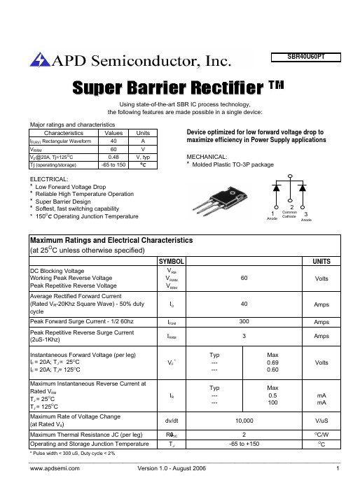
__SBR40U60PTUsing state-of-the-art SBR IC process technology,the following features are made possible in a single device:Major ratings and characteristicsCharacteristicsValues UnitsDevice optimized for low forward voltage drop to maximize efficiency in Power Supply applications I F(AV) 40Rectangular Waveform A V RRM60V V F @20A, Tj=125O C0.48V, typ MECHANICAL:Tj -65 to 150(operating/storage)O C* Molded Plastic TO-3P packageELECTRICAL:* Low Forward Voltage Drop* Reliable High Temperature Operation * Super Barrier Design* Softest, fast switching capability* 150O C Operating Junction TemperatureMaximum Ratings and Electrical Characteristics (at 25O C unless otherwise specified)SYMBOL UNITSDC Blocking VoltageWorking Peak Reverse Voltage Peak Repetitive Reverse VoltageV RM V RWM V RRM60VoltsAverage Rectified Forward Current(Rated V R -20Khz Square Wave) - 50% duty cycleI O 40Amps Peak Forward Surge Current - 1/2 60hz I FSM 300Amps Peak Repetitive Reverse Surge Current (2uS-1Khz)I RRM3AmpsInstantaneous Forward Voltage (per leg)I F = 20A; T J = 25O CI F = 20A; T J = 125O C V F *Typ ------Max 0.690.60VoltsMaximum Instantaneous Reverse Current at Rated V RM T J = 25O CT J = 125O CI RTyp ------Max 0.5100mA mA Maximum Rate of Voltage Change (at Rated V R )dv/dt 10,000V/uSMaximum Thermal Resistance JC (per leg)R θJC 2OC/WOperating and Storage Junction TemperatureT J-65 to +150OC* Pulse width < 300 uS, Duty cycle < 2%______________________________________________________________________________________________ Version 1.0 - August 2006113AnodeCommon CathodeAnode__SBR40U60PTFigure 1: Typical Reverse Current (per leg)Figure 2: Typical Forward Voltage (per leg)Figure 3: Current Derating, Case (per leg)______________________________________________________________________________________________ Version 1.0 - August 20062APD SEMICONDUCTOR reserves the right to make changes without further notice to any products herein. APD SEMICONDUCTOR makes no warranty, representation or guarantee regarding the suitability of its products for any particular purpose, nor does APD SEMICONDUCTOR assume any liability arising out of the application or use of any product or circuit, and specifically disclaims any and all liability, including without limitation special, consequential or incidental damages. “Typical” parameters which may be provided in APD SEMICONDUCTOR data sheets and/or specifications can and do vary in different applications and actual performance may vary over time. All operating parameters, including “Typicals” must be validated for each customer application by customer’s technical experts. APD SEMICONDUCTOR does not convey any license under its patent rights nor the rights of others. APD SEMICONDUCTOR products are not designed, intended, or authorized for use as components in systems intended for surgical implant into the body, or otherapplications intended to support or sustain life, or for any other application in which the failure of the APD SEMICONDUCTOR product could create a situation where personal injury or death may occur. Should Buyer purchase or use APD SEMICONDUCTOR products for any such unintended or unauthorized application, Buyer shall indemnify and hold APD SEMICONDUCTOR and its officers, employees, subsidiaries, affiliates, and distributors harmless against all claims, costs, damages, and expenses, and reasonable attorney fees arising out of, directly or indirectly, any claim of personal injury or death associated with such unintended orunauthorized use, even if such claim alleges that APD SEMICONDUCTOR was negligent regarding the design or manufacture of the part..1 Lagoon Drive, Suite 410, Redwood City, CA 94065, USA Ph: 650 508 8896 FAX: 650 508 8865Homepage: email: info@。
SBR40U300CT;中文规格书,Datasheet资料

• Ultra Low Forward Voltage Drop • Low Leakage Current • Excellent High Temperature Stability • Patented Super Barrier Rectifier Technology • Soft, Fast Switching Capability • 175ºC Operating Junction Temperature • Lead Free Finish, RoHS Compliant (Note 1) • Also Available in Green Molding Compound (Note 2)
0.1
0
50 100 150 200 250 300
VR, INSTANTANEOUS REVERSE VOLTAGE (V)
Fig. 2 Typical Reverse Characteristics
SBR is a registered trademark of Diodes Incorporated.
Marking Information
SBR
40U300CT
YYWW AB
SBR40U300CT = Product Type Marking Code AB = Foundry and Assembly Code YYWW = Date Code Marking YY = Last two digits of year (ex: 07 = 2007) WW = Week (01 - 53)
0INSTANTANEOUS FORWARD VOLTAGE (V) Fig.1 Typical Forward Characteristics
SN54HC4060 - 数字逻辑集成电路说明书

SN54HC4060, SN74HC406014ĆSTAGE ASYNCHRONOUS BINARY COUNTERS AND OSCILLATORSSCLS161D − DECEMBER 1982 − REVISED SEPTEMBER 2003D Wide Operating Voltage Range of 2 V to 6 V D Outputs Can Drive Up To 10 LSTTL Loads D Low Power Consumption, 80-µA Max I CC DTypical t pd = 14 nsD ±4-mA Output Drive at 5 VD Low Input Current of 1 µA Max D Allow Design of Either RC- orCrystal-Oscillator CircuitsSN54HC4060...J OR W PACKAGESN74HC4060...D, DB, N, NS, OR PW PACKAGE(TOP VIEW)SN54HC4060...FK PACKAGE(TOP VIEW)NC − No internal connection12345678161514131211109Q L Q M Q N Q F Q E Q G Q D GNDV CC Q J Q H Q I CLR CLKI CLKO CLKO3212019910111213456781817161514Q H Q I NC CLR CLKIQ N Q F NC Q E Q GQ Q N C C L K OV Q DG N D N C C CMLJQ C L K O description/ordering informationThe ’HC4060 devices consist of an oscillator section and 14 ripple-carry binary counter stages. The oscillator configuration allows design of either RC- or crystal-oscillator circuits. A high-to-low transition on the clock (CLKI)input increments the counter. A high level at the clear (CLR) input disables the oscillator (CLKO goes high and CLKO goes low) and resets the counter to zero (all Q outputs low).ORDERING INFORMATIONT APACKAGE †ORDERABLE PART NUMBER TOP-SIDE MARKING PDIP − N Tube of 25SN74HC4060N SN74HC4060NTube of 40SN74HC4060D Reel of 2500SN74HC4060DR SOIC − DReel of 250SN74HC4060DT HC4060°°SOP − NS Reel of 2000SN74HC4060NSR HC4060−40C to 85CSSOP − DB Reel of 2000SN74HC4060DBR HC4060Tube of 90SN74HC4060PW Reel of 2000SN74HC4060PWR TSSOP − PW Reel of 250SN74HC4060PWT HC4060CDIP − JTube of 25SNJ54HC4060J SNJ54HC4060J °°CFP − W Tube of 150SNJ54HC4060W SNJ54HC4060W −55C to 125CLCCC − FKTube of 55SNJ54HC4060FKSNJ54HC4060FK †Package drawings, standard packing quantities, thermal data, symbolization, and PCB design guidelines are available at /sc/package.Copyright 2003, Texas Instruments IncorporatedPRODUCTION DATA information is current as of publication date.Please be aware that an important notice concerning availability, standard warranty, and use in critical applications of Texas Instruments semiconductor products and disclaimers thereto appears at the end of this data sheet.SN54HC4060, SN74HC406014ĆSTAGE ASYNCHRONOUS BINARY COUNTERS AND OSCILLATORSSCLS161D − DECEMBER 1982 − REVISED SEPTEMBER 2003FUNCTION TABLE (each buffer)INPUTS CLK CLR FUNCTION ↑L No change ↓L Advance to next stageXHAll outputs Llogic diagram (positive logic)Pin numbers shown are for the D, DB, J, N, NS, PW, and W packages.R TR TR TR TR TR TR TR T614131512311CLKIQ IQ LQ MQ NQ GQ HQ JR T4Q FR TR TR TR TR T75Q DQ E12CLR910CLKO CLKOabsolute maximum ratings over operating free-air temperature range (unless otherwise noted)†Supply voltage range, V CC −0.5 V to 7 V . . . . . . . . . . . . . . . . . . . . . . . . . . . . . . . . . . . . . . . . . . . . . . . . . . . . . . . . . . Input clamp current, I IK (V I < 0 or V I > V CC ) (see Note 1) ±20 mA . . . . . . . . . . . . . . . . . . . . . . . . . . . . . . . . . . . . Output clamp current, I OK (V O < 0 or V O > V CC ) (see Note 1) ±20 mA . . . . . . . . . . . . . . . . . . . . . . . . . . . . . . . . Continuous output current, I O (V O = 0 to V CC ) ±25 mA . . . . . . . . . . . . . . . . . . . . . . . . . . . . . . . . . . . . . . . . . . . . . . Package thermal impedance, θJA (see Note 2):D package 73°C/W. . . . . . . . . . . . . . . . . . . . . . . . . . . . . . . . . . . DB package 82°C/W . . . . . . . . . . . . . . . . . . . . . . . . . . . . . . . . . N package 67°C/W . . . . . . . . . . . . . . . . . . . . . . . . . . . . . . . . . . . NS package 64°C/W . . . . . . . . . . . . . . . . . . . . . . . . . . . . . . . . . PW package 108°C/W. . . . . . . . . . . . . . . . . . . . . . . . . . . . . . . . Storage temperature range, T stg −65°C to 150°C. . . . . . . . . . . . . . . . . . . . . . . . . . . . . . . . . . . . . . . . . . . . . . . . . . . †Stresses beyond those listed under “absolute maximum ratings” may cause permanent damage to the device. These are stress ratings only, and functional operation of the device at these or any other conditions beyond those indicated under “recommended operating conditions” is not implied. Exposure to absolute-maximum-rated conditions for extended periods may affect device reliability.NOTES: 1.The input and output voltage ratings may be exceeded if the input and output current ratings are observed.2.The package thermal impedance is calculated in accordance with JESD 51-7.SN54HC4060, SN74HC406014ĆSTAGE ASYNCHRONOUS BINARY COUNTERS AND OSCILLATORSSCLS161D − DECEMBER 1982 − REVISED SEPTEMBER 2003recommended operating conditions (see Note 3)SN54HC4060SN74HC4060MINNOMMAXMIN NOMMAXUNIT V CC Supply voltage 256256VV CC = 2 V 1.5 1.5V V CC = 4.5 V 3.15 3.15IHHigh-level input voltageV CC = 6 V 4.24.2VV CC = 2 V0.50.5V V CC = 4.5 V 1.35 1.35IL Low-level input voltage V CC = 6 V1.8 1.8V V I Input voltage 0V CC 0V CC V V O Output voltage0V CC 0V CC V V CC = 2 V 10001000V CC = 4.5 V 500500∆t/∆vInput transition rise/fall timeV CC = 6 V 400400ns T A Operating free-air temperature −55125−4085°C NOTE 3:All unused inputs of the device must be held at V CC or GND to ensure proper device operation. Refer to the TI application report,Implications of Slow or Floating CMOS Inputs , literature number SCBA004.electrical characteristics over recommended operating free-air temperature range (unless otherwise noted)V CC T A = 25°C SN54HC4060SN74HC4060PARAMETERTEST CONDITIONSMIN TYP MAX MIN MAXMIN MAXUNIT2 V1.9 1.998 1.9 1.9V I OH = −20 µA4.5 V 4.4 4.499 4.4 4.4V All outputsI = V IH or V IL ,6 V 5.9 5.999 5.9 5.9OHV I OH = −4 mA 4.5 V 3.98 4.3 3.7 3.84VQ outputsI = V IH or V ILI OH = −5.2 mA 6 V 5.485.8 5.25.342 V0.0020.10.10.1V I OL = 20 µA 4.5 V 0.0010.10.10.1V All outputsI = V IH or V IL ,6 V 0.0010.10.10.1OLV I OL = 4 mA 4.5 V 0.170.260.40.33V Q outputsI = V IH or V IL I OL = 5.2 mA 6 V 0.150.260.40.33I I V I = V CC or 0 6 V ±0.1±100±1000±1000nA I CC V I = V CC or 0,I O = 06 V 816080µA C i2 V to 6 V3101010pFSN54HC4060, SN74HC406014ĆSTAGE ASYNCHRONOUS BINARY COUNTERS AND OSCILLATORSSCLS161D − DECEMBER 1982 − REVISED SEPTEMBER 2003timing requirements over recommended operating free-air temperature range (unless otherwise noted)V CC T A = 25°C SN54HC4060SN74HC4060MIN MAXMINMAX MINMAX UNIT2 V5.5 3.7 4.3f clock4.5 V 281922Clock frequency6 V 332225MHz 2 V901351154.5 V 182723t CLKI high or low6 V 152320wPulse duration2 V 90135115ns4.5 V 182723CLR high6 V 1523202 V160240200t su4.5 V 324840Setup time, CLR inactive before CLKI ↓6 V274134ns switching characteristics over recommended operating free-air temperature range, C L = 50 pF(unless otherwise noted) (see Figure 1)FROM TO V CC T A = 25°C SN54HC4060SN74HC4060PARAMETER(INPUT)(OUTPUT)MIN TYP MAX MIN MAXMIN MAXUNIT2 V5.510 3.7 4.3max4.5 V 28451922f 6 V 33532225MHz2 V240490735615t pd4.5 V 5898147123CLKIQ D6 V 4283125105ns 2 V66140210175t PHL4.5 V 18284235CLRAny Q6 V 14243630ns 2 V287511095t t4.5 V 8152219Any6 V6301916ns operating characteristics, T A = 25°CPARAMETERTEST CONDITIONSTYP UNIT C pdPower dissipation capacitanceNo load88pFSN54HC4060, SN74HC406014ĆSTAGE ASYNCHRONOUS BINARY COUNTERS AND OSCILLATORSSCLS161D − DECEMBER 1982 − REVISED SEPTEMBER 2003PARAMETER MEASUREMENT INFORMATIONVOLTAGE WAVEFORMSSETUP AND INPUT RISE AND FALL TIMESVOLTAGE WAVEFORMS PULSE DURATIONSt su 50%50%50%10%10%90%90%V CC V CC0 V0 Vt rt fReferenceInputData Input50%High-LevelPulse50%V CC0 V 50%50%V CC0 Vt wLow-LevelPulseVOLTAGE WAVEFORMSPROPAGATION DELAY AND OUTPUT TRANSITION TIMES 50%50%50%10%10%90%90%V CC V OHV OL 0 Vt rt fInputIn-Phase Output50%t PLHt PHL 50%50%10%10%90%90%V OH V OLt rt f t PHLt PLH Out-of-PhaseOutputTest Point From Output Under TestLOAD CIRCUITNOTES: A.C L includes probe and test-fixture capacitance.B.Phase relationships between waveforms were chosen arbitrarily. All input pulses are supplied by generators having the followingcharacteristics: PRR ≤ 1 MHz, Z O = 50 Ω, t r = 6 ns, t f = 6 ns.C.For clock inputs, f max is measured when the input duty cycle is 50%.D.The outputs are measured one at a time with one input transition per measurement.E.t PLH and t PHL are the same as t pd .C L = 50 pF (see Note A)Figure 1. Load Circuit and Voltage WaveformsSN54HC4060, SN74HC406014ĆSTAGE ASYNCHRONOUS BINARY COUNTERS AND OSCILLATORSSCLS161D − DECEMBER 1982 − REVISED SEPTEMBER 2003CONNECTING AN RC-OSCILLATOR CIRCUIT TO THE ’HC4060 DEVICESThe ’HC4060 devices consist of an oscillator section and 14 ripple-carry binary counter stages. The oscillator configuration allows design of either RC- or crystal-oscillator circuits.When an RC-oscillator circuit is implemented, two resistors and a capacitor are required. The components are attached to the terminals as shown:1 2 3 4 5 6 7 8161514131211109R2R1CTo determine the values of capacitance and resistance necessary to obtain a specific oscillator frequency (f), use this formula:f+12(R1)(C)ǒ0.405R2R1)R2)0.693ǓIf R2 > > R1 (i.e., R2 = 10R1), the above formula simplifies to:f+0.455RCPACKAGING INFORMATION(1) The marketing status values are defined as follows:ACTIVE: Product device recommended for new designs.LIFEBUY: TI has announced that the device will be discontinued, and a lifetime-buy period is in effect.NRND: Not recommended for new designs. Device is in production to support existing customers, but TI does not recommend using this part in a new design.PREVIEW: Device has been announced but is not in production. Samples may or may not be available.OBSOLETE: TI has discontinued the production of the device.(2) RoHS: TI defines "RoHS" to mean semiconductor products that are compliant with the current EU RoHS requirements for all 10 RoHS substances, including the requirement that RoHS substance do not exceed 0.1% by weight in homogeneous materials. Where designed to be soldered at high temperatures, "RoHS" products are suitable for use in specified lead-free processes. TI may reference these types of products as "Pb-Free".RoHS Exempt: TI defines "RoHS Exempt" to mean products that contain lead but are compliant with EU RoHS pursuant to a specific EU RoHS exemption.Green: TI defines "Green" to mean the content of Chlorine (Cl) and Bromine (Br) based flame retardants meet JS709B low halogen requirements of <=1000ppm threshold. Antimony trioxide based flame retardants must also meet the <=1000ppm threshold requirement.Addendum-Page 1(3) MSL, Peak Temp. - The Moisture Sensitivity Level rating according to the JEDEC industry standard classifications, and peak solder temperature.(4) There may be additional marking, which relates to the logo, the lot trace code information, or the environmental category on the device.(5) Multiple Device Markings will be inside parentheses. Only one Device Marking contained in parentheses and separated by a "~" will appear on a device. If a line is indented then it is a continuation of the previous line and the two combined represent the entire Device Marking for that device.(6) Lead finish/Ball material - Orderable Devices may have multiple material finish options. Finish options are separated by a vertical ruled line. Lead finish/Ball material values may wrap to two lines if the finish value exceeds the maximum column width.Important Information and Disclaimer:The information provided on this page represents TI's knowledge and belief as of the date that it is provided. TI bases its knowledge and belief on information provided by third parties, and makes no representation or warranty as to the accuracy of such information. Efforts are underway to better integrate information from third parties. TI has taken and continues to take reasonable steps to provide representative and accurate information but may not have conducted destructive testing or chemical analysis on incoming materials and chemicals. TI and TI suppliers consider certain information to be proprietary, and thus CAS numbers and other limited information may not be available for release.In no event shall TI's liability arising out of such information exceed the total purchase price of the TI part(s) at issue in this document sold by TI to Customer on an annual basis.OTHER QUALIFIED VERSIONS OF SN54HC4060, SN74HC4060 :•Catalog : SN74HC4060•Automotive : SN74HC4060-Q1, SN74HC4060-Q1•Military : SN54HC4060NOTE: Qualified Version Definitions:•Catalog - TI's standard catalog product•Automotive - Q100 devices qualified for high-reliability automotive applications targeting zero defects•Military - QML certified for Military and Defense ApplicationsAddendum-Page 2TAPE AND REEL INFORMATIONA0B0K0W Dimension designed to accommodate the component length Dimension designed to accommodate the component thickness Overall width of the carrier tapePitch between successive cavity centersDimension designed to accommodate the component width TAPE DIMENSIONSSprocket HolesP1*All dimensions are nominalDevicePackage Type Package Drawing Pins SPQReel Diameter (mm)Reel Width W1 (mm)A0(mm)B0(mm)K0(mm)P1(mm)W (mm)Pin1Quadrant SN74HC4060DBR SSOP DB 162000330.016.48.35 6.6 2.412.016.0Q1SN74HC4060DR SOIC D 162500330.016.4 6.510.3 2.18.016.0Q1SN74HC4060NSR SO NS 162000330.016.48.210.5 2.512.016.0Q1SN74HC4060PWR TSSOP PW 162000330.012.4 6.9 5.6 1.68.012.0Q1SN74HC4060PWR TSSOP PW 162000330.012.4 6.9 5.6 1.68.012.0Q1SN74HC4060PWRG4TSSOP PW 162000330.012.4 6.9 5.6 1.68.012.0Q1SN74HC4060PWTTSSOPPW16250330.012.46.95.61.68.012.0Q1*All dimensions are nominalDevice Package Type Package Drawing Pins SPQ Length (mm)Width (mm)Height (mm) SN74HC4060DBR SSOP DB162000356.0356.035.0 SN74HC4060DR SOIC D162500340.5336.132.0 SN74HC4060NSR SO NS162000356.0356.035.0 SN74HC4060PWR TSSOP PW162000356.0356.035.0 SN74HC4060PWR TSSOP PW162000364.0364.027.0 SN74HC4060PWRG4TSSOP PW162000356.0356.035.0 SN74HC4060PWT TSSOP PW16250356.0356.035.0PACKAGE MATERIALS INFORMATION 1-Jul-2023 TUBET - Tube*All dimensions are nominalDevice Package Name Package Type Pins SPQ L (mm)W (mm)T (µm) B (mm) SN54HC4060FK FK LCCC201506.9812.062030NASN74HC4060D D SOIC164050783940 4.32SN74HC4060D D SOIC1640506.683940 4.32SN74HC4060N N PDIP162550613.9711230 4.32SN74HC4060N N PDIP162550613.9711230 4.32SN74HC4060PW PW TSSOP169053010.23600 3.5PACKAGE OUTLINETSSOP - 1.2 mm max heightPW0016A SMALL OUTLINE PACKAGENOTES:1. All linear dimensions are in millimeters. Any dimensions in parenthesis are for reference only. Dimensioning and tolerancing per ASME Y14.5M.2. This drawing is subject to change without notice.3. This dimension does not include mold flash, protrusions, or gate burrs. Mold flash, protrusions, or gate burrs shall notexceed 0.15 mm per side.4. This dimension does not include interlead flash. Interlead flash shall not exceed 0.25 mm per side.5. Reference JEDEC registration MO-153.EXAMPLE BOARD LAYOUTTSSOP - 1.2 mm max heightPW0016A SMALL OUTLINE PACKAGENOTES: (continued)6. Publication IPC-7351 may have alternate designs.7. Solder mask tolerances between and around signal pads can vary based on board fabrication site.EXAMPLE STENCIL DESIGNTSSOP - 1.2 mm max heightPW0016A SMALL OUTLINE PACKAGENOTES: (continued)8. Laser cutting apertures with trapezoidal walls and rounded corners may offer better paste release. IPC-7525 may have alternate design recommendations.9. Board assembly site may have different recommendations for stencil design.PACKAGE OUTLINESSOP - 2 mm max heightDB0016A SMALL OUTLINE PACKAGENOTES:1. All linear dimensions are in millimeters. Any dimensions in parenthesis are for reference only. Dimensioning and tolerancing per ASME Y14.5M.2. This drawing is subject to change without notice.3. This dimension does not include mold flash, protrusions, or gate burrs. Mold flash, protrusions, or gate burrs shall notexceed 0.15 mm per side.4. Reference JEDEC registration MO-150.EXAMPLE BOARD LAYOUTSSOP - 2 mm max heightDB0016A SMALL OUTLINE PACKAGENOTES: (continued)5. Publication IPC-7351 may have alternate designs.6. Solder mask tolerances between and around signal pads can vary based on board fabrication site.EXAMPLE STENCIL DESIGNSSOP - 2 mm max heightDB0016A SMALL OUTLINE PACKAGENOTES: (continued)7. Laser cutting apertures with trapezoidal walls and rounded corners may offer better paste release. IPC-7525 may have alternate design recommendations.8. Board assembly site may have different recommendations for stencil design.GENERIC PACKAGE VIEWThis image is a representation of the package family, actual package may vary.Refer to the product data sheet for package details.LCCC - 2.03 mm max height FK 20LEADLESS CERAMIC CHIP CARRIER8.89 x 8.89, 1.27 mm pitch 4229370\/A\PACKAGE OUTLINESOP - 2.00 mm max heightNS0016A SOPNOTES:1. All linear dimensions are in millimeters. Dimensions in parenthesis are for reference only. Dimensioning and tolerancingper ASME Y14.5M.2. This drawing is subject to change without notice.3. This dimension does not include mold flash, protrusions, or gate burrs. Mold flash, protrusions, or gate burrs shall notexceed 0.15 mm, per side.4. This dimension does not include interlead flash. Interlead flash shall not exceed 0.25 mm, per side.EXAMPLE BOARD LAYOUTSOP - 2.00 mm max heightNS0016A SOPNOTES: (continued)5. Publication IPC-7351 may have alternate designs.6. Solder mask tolerances between and around signal pads can vary based on board fabrication site.EXAMPLE STENCIL DESIGNSOP - 2.00 mm max heightNS0016A SOPNOTES: (continued)7. Laser cutting apertures with trapezoidal walls and rounded corners may offer better paste release. IPC-7525 may have alternate design recommendations.8. Board assembly site may have different recommendations for stencil design.IMPORTANT NOTICE AND DISCLAIMERTI PROVIDES TECHNICAL AND RELIABILITY DATA (INCLUDING DATA SHEETS), DESIGN RESOURCES (INCLUDING REFERENCE DESIGNS), APPLICATION OR OTHER DESIGN ADVICE, WEB TOOLS, SAFETY INFORMATION, AND OTHER RESOURCES “AS IS” AND WITH ALL FAULTS, AND DISCLAIMS ALL WARRANTIES, EXPRESS AND IMPLIED, INCLUDING WITHOUT LIMITATION ANY IMPLIED WARRANTIES OF MERCHANTABILITY, FITNESS FOR A PARTICULAR PURPOSE OR NON-INFRINGEMENT OF THIRD PARTY INTELLECTUAL PROPERTY RIGHTS.These resources are intended for skilled developers designing with TI products. You are solely responsible for (1) selecting the appropriate TI products for your application, (2) designing, validating and testing your application, and (3) ensuring your application meets applicable standards, and any other safety, security, regulatory or other requirements.These resources are subject to change without notice. TI grants you permission to use these resources only for development of an application that uses the TI products described in the resource. Other reproduction and display of these resources is prohibited. No license is granted to any other TI intellectual property right or to any third party intellectual property right. TI disclaims responsibility for, and you will fully indemnify TI and its representatives against, any claims, damages, costs, losses, and liabilities arising out of your use of these resources.TI’s products are provided subject to TI’s Terms of Sale or other applicable terms available either on or provided in conjunction with such TI products. TI’s provision of these resources does not expand or otherwise alter TI’s applicable warranties or warranty disclaimers for TI products.TI objects to and rejects any additional or different terms you may have proposed.Mailing Address: Texas Instruments, Post Office Box 655303, Dallas, Texas 75265Copyright © 2023, Texas Instruments Incorporated。
BA60BC0FP中文资料
The products listed in this document are designed to be used with ordinary electronic equipment or devices (such as audio visual equipment, office-automation equipment, communications devices, electrical appliances and electronic toys). Should you intend to use these products with equipment or devices which require an extremely high level of reliability and the malfunction of with would directly endanger human life (such as medical instruments, transportation equipment, aerospace machinery, nuclear-reactor controllers, fuel controllers and other safety devices), please be sure to consult with our sales representative in advance. About Export Control Order in Japan Products described herein are the objects of controlled goods in Annex 1 (Item 16) of Export Trade Control Order in Japan. In case of export from Japan, please confirm if it applies to "objective" criteria or an "informed" (by MITI clause) on the basis of "catch all controls for Non-Proliferation of Weapons of Mass Destruction.
AP4060规格书
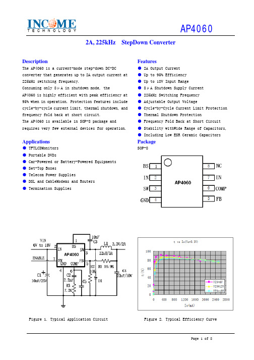
2A, 225kHz StepDown ConverterFigure 1. Typical Application Circuit Figure 2. Typical Efficiency CurveDescription The AP4060 is a current-mode step-down DC-DC converter that generates up to 2A output current at 225kHz switching frequency. Consuming only 8μA in shutdown mode, the AP4060 is highly efficient with peak efficiency at 95% when in operation. Protection features include cycle-by-cycle current limit, thermal shutdown, and frequency fold back at short circuit. The AP4060 is available in SOP-8 package and requires very few external devices for operation. Applications ● TFTLCDMonitors ● Portable DVDs ● Car-Powered or Battery-Powered Equipments ● Set-Top Boxes ● Telecom Power Supplies ● DSL and CableModems and Routers ● Termination Supplies Features ● 2A Output Current ● Up to 95% Efficiency ● Up to 18V Input Range ● 8μA Shutdown Supply Current ● 225kHz Switching Frequency ● Adjustable Output Voltage ● Cycle-by-Cycle Current Limit Protection ● Thermal Shutdown Protection ● Frequency Fold Back at Short Circuit ● Stability withWide Range of Capacitors, ● Including Low ESR Ceramic Capacitors PackageSOP-8AbsoluteMaximumRatings(Note: Do not exceed these limits to prevent damage to the device. Exposure to absolute maximum rating conditions for long periods may affect device reliability.)PARAMETER VALUE UNITIN Supply Voltage -0.3 to 18VSW Voltage-1 to V IN + 1VBS Voltage V SW–0.3 to V SW+ 8VEN, FB, COMP Voltage-0.3 to 6VContinuous SW Current Internally limited AJunction to Ambient Thermal Resistance (θJA)105°C/WOperating Junction Temperature-40 to 150°CStorage Temperature-55 to 1°CLead Temperature (Soldering, 10 sec)300°CElectricalCharacteristics(V IN = 12V, T J = 25 C unless otherwise specified)PARAMETER SYMBO TEST CONDITIONS MIN TYP MAX UNIT Input Voltage VIN V OUT = 5V, I LOAD = 1A 6 18 V Input UVLO 4.0 V Feedback Voltage VFB V COMP= 1.5V 1.196 1.22 1.244VHigh-Side Switch On Resistance RONH 0.3 ΩLow-Side Switch On Resistance RONL 8 ΩSW Leakage V EN = 0 0 10 µA Current Limit ILIM 3 3.3 ACOMP to Current Limit Transconductance GCOMP1.8 A/VError Amplifier Transconductance GEA ∆I COMP= ±10µA 550 µA/V Error Amplifier DC Gain AVEA 4000V/V Switching Frequency fSW 190 225240kHz Short Circuit Switching Frequency V FB= 050kHz Maximum Duty Cycle DMAX V FB= 1.1V92% Minimum Duty Cycle V FB= 1.3V0% Enable Threshold Voltage Hysteresis = 0.2V0.51 1.3V Enable Pull Up Current Pin pulled up to 4.5V typicallywhen left unconnected1µA Supply Current in Shutdown V EN = 0 8 20 µA IC Supply Current in Operation V EN =3V, V FB=1.3V 0.7 mA Soft-start Period 10 ms Thermal Shutdown 150 °CFigure 3. Functional Block DiagramFunctional DescriptionAs seen in Figure 2, Functional Block Diagram,the AP4060 is a current mode pulse widthmodulation (PWM) converter. The converter operatesas follows:A switching cycle starts when the rising edgeof the Oscillator clock output causes the High- Side Power Switch to turn on and the Low-Side Power Switch to turn off. With the SW side of the inductor now connected to IN, the inductor current ramps up to store energy in the its magnetic field. The inductor current level is measured by the Current Sense Amplifier and added to the Oscillator ramp signal. If the resulting summation is higher than the COMP voltage, the output of the PWM Comparator goes high.Whenthis happens or when Oscillatorclock output goes low, the High-Side Power Switch turns off and the Low-Side Power Switch turns on. At this point, the SW side of the inductor swings to a diode voltage below ground, causing the inductor current to decrease and magnetic energy to be transferred to output. This state continues until the cycle starts again.The High-Side Power Switch is driven by logicusing BS bootstrap pin as the positive rail. This pin is charged to V SW + 6V when the Low-Side Power Switch turns on.The COMP voltage is the integration of the error between FB input and the internal 1.293Vreference. If FB is lower than the reference voltage, COMP tends to go higher to increase current to the output. Current limit happens when COMP reachesits maximum clamp value of 2.55V.The Oscillator normally switches at 225kHz. However, if FB voltage is less than 0.7V, then the switching frequency decreases until it reaches a minimum of 50kHz at V FB = 0.5V.SHUTDOWN CONTROLThe AP4060 has an enable input EN for turning theIC on or off. When EN is less than 0.7V, the IC is in 8μA low current shutdown mode. When EN is higher than 1.3V, the IC is in normal operation mode. EN is internally pulled up with a 1μA current source and can be left unconnected for always-on operation. Note that EN is a low voltage input with a maximum voltage of 6V; it should never be directly connected to IN. THERMAL SHUTDOWNThe AP4060 automatically turns off when itsjunction temperature exceeds 150°C.Application InformationOUTPUT VOLTAGE SETTINGFigure 3. Output Voltage SettingFigure 3 shows the connections for setting theoutput voltage. Select the proper ratio of the twofeedback resistors R FB1 and R FB2 based on theoutput voltage. Typically, use R FB2≈10kΩ anddetermine R FB1 from the output voltage:INPUT CAPACITORThe input capacitor needs to be carefully selectedto maintain sufficiently low ripple at the supplyinputof the converter. A low ESR capacitor is highlyrecommended. Since large current flows in and out ofthis capacitor during switching, its ESR also affectsefficiency.The input capacitance needs to be higher than10μF. The best choice is the ceramic type; however,low ESR tantalum or electrolytic types may also beused provided that the RMS ripple current rating ishigher than 50% of the output current. The inputcapacitor should be placed close to the IN and Gpins of the IC, with shortest traces possible. In thecase of tantalum or electrolytic types, they can befurther away if a small parallel 0.1μF ceramiccapacitor is placed right next to the IC.OUTPUT CAPACITORThe output capacitor also needs to have low ESRto keep low output voltage ripple. The outputripple voltage is:INDUCTOR SELECTIONThe inductor maintains a continuous current tothe output load. This inductor current has a ripplethat is dependent on the inductance value: higherinductance reduces the peak-to-peak ripplecurrent. The trade off for high inductance value isthe increase in inductor core size and seriesresistance, and the reduction in current handlingcapability. In general, select an inductance value Lbased on ripple current requirement:where V IN is the input voltage, V OUT is the outputvoltage, f SW is the switching frequency, I OUTMAX is themaximum output current, and K RIPPLE is the ripplefactor. Typically, choose K RIPPLE= 30%to correspond tothe peak-to-peak ripple current being 30% of themaximum output current.With this inductor value (Table 1), the peakinductor current is I OUT•(1+K RIPPLE / 2). Make surethat this peak inductor current is less that the 3Acurrent limit. Finally, select the inductor core sizeso that it does not saturate at 3A.Table 1. Typical Inductor ValuesV OUT 1.5V 1.8V 2.5V 3.3V 5VL 10μH10μH15μH22μH33μHwhere I OUTMAX is the maximum output current,K RIPPLE is the ripple factor, R ESR is the ESRresistance of the output capacitor, f SW is theswitching frequency,L in the inductor value, C OUTis the output capacitance.In the case of ceramicoutput capacitors, R ESR is very small and does notcontribute to the ripple. Therefore, a lowercapacitance value can be used for ceramic type.In the case of tantalum or electrolytic type,the ripple is dominated by R ESR multiplied by theripple current. In that case, the output capacitorischosen to have sufficiently low ESR.For ceramic output type, typically choose acapacitance of about 22μF. For tantalum orelectrolytic type, choose a capacitor with lessthan 50mΩ ESR.RECTIFIER DIODEUse a Schottky diode as the rectifier toconduct current when the High-Side Power Switchis off. The Schottky diode must have currentrating input voltage.STABILITY COMPENSATIONFigure 4. Stability CompensationThe dominant pole P1 is due to CCOMPThe second pole P2 is the output pole:The first zero Z1 is due to R COMP and C COMP:And finally, the third pole is due to R COMP and C COMP2 (if C COMP2 is used):Follow the following steps to compensate the IC:STEP 1. Set the cross over frequency at 1/5 of the switching frequency via R COMP :but limit R COMP to 15kΩ maximum.STEP 2. Set the zero f Z1 at 1/4 of the cross over frequency. If R COMP is less than 15kΩ, the equation for C COMP is: The feedback system of the IC is stabilized by the components at COMP pin, as shown in Figure 4.The DC loop gain of the system is determined by the following equation:If R COMP is limited to 15kΩ, then the actual cross over frequency is 3.4 / (V OUT C OUT).Therefore:STEP 3. If the output capacitor’s ESR is high enoughto cause a zero at lower than 4 times the cross over frequency, an additional compensationcapacitor C COMP2 is required. The condition for using C COMP2 is:And the proper value for Ccomp2 is:Though C COMP2 is unnecessary when the output capacitor has sufficiently low ESR, a small value C COMP2 such as 100pF may improve stability against PCB layout parasitic effects.Table 2. Typical Compensation for Different Output Voltages and Output Capacitors V outC outR compC compC comp22.5V 22µF Ceramic 5.6 k Ω 6.8 nF None3.3V 22µF Ceramic 7.2 k Ω 2.2 nF None 5V 22µF Ceramic 10k Ω 1.5nF None 2.5V 47µF SP Cap 15k Ω1.5nFNone 3.3V 47µF SP Cap 15K Ω 1.8nF None 5V 47µF SP Cap 15k Ω 2.7nF None 2.5V470µF/6.3V/30m Ω 15k Ω 15nF 1nF 3.3V 470µF/6.3V/30m Ω 15k Ω 22nF 1nF 5V 470µF/10V/30m Ω15k Ω27nFNoneFigure 4 shows a sample AP4060 application circuit generating 2.5V/2A output.Figure 4. AP4060 2.5V/2A Output ApplicationTypical Performence CharacteristicsOrdering InformationPART NUMBER MARK1TEMPERATURERANGEPACKAGE PINSAP40602920YYWW1-40℃to 85℃SOP-881. Y= Year.W = Week.Pin ConfigurationPin DescriptionPIN NUMBERPINNAMEPIN DESCRIPTION1 BS Bootstrap. This pin acts as the positive rail for the high-side switch’s gate driver.Connect a 10nF between this pin and SW.2 IN Input Supply. Bypass this pin to G with a low ESR capacitor. See Input Capacitor inApplication Information section.3 SWSwitch Output. Connect this pin to the switching end of the inductor.4 GGround.5 FBFeedback Input. The voltage at this pin is regulated to 1.22V. Connect to the resistordivider between output and ground to set output voltage.6 COMPCompensation Pin. See Compensation Technique in Application Information section.7 ENEnable Input. When higher than 1.3V, this pin turns the IC on. When lower than 0.7V,this pin turns the IC off. Output voltage is discharged when the IC is off. This pin has asmall internal pull up current to a high level voltage when pin is not connected.8 N/CNot Connected.PackageOutlineSOP-8 PACKAGEOUTLINEAND DIMENSIONSSYMBOL DIMENSION IN MILIMETERS DIMENSION IN INCHESA 1.350 1.750 0.053 0.069A 0.100 0.250 0.004 0.010A 1.350 1.550 0.053 0.061B 0.330 0.510 0.013 0.020C 0.190 0.250 0.007 0.010D 4.780 5.000 0.188 0.197E 3.800 4.000 0.150 0.157E 5.800 6.300 0.228 0.248e 1.270 TYP 0.050 TYPL 0.400 1.270 0.016 0.0500 0 8 0 8。
SBR3A40SA-13;中文规格书,Datasheet资料

3.0A SBRSUPER BARRIER RECTIFIERSMAFeatures• Low Leakage Current • Patented Super Barrier Rectifier Technology • Soft, Fast Switching Capability • 150ºC Operating Junction Temperature • Lead Free Finish, RoHS Compliant (Note 1) • Green Molding Compound (No Halogen and Antimony)(Note 7)Mechanical Data• Case: SMA • Case Material: Molded Plastic, UL Flammability ClassificationRating 94V-0 • Moisture Sensitivity: Level 1 per J-STD-020D • Terminals: Lead Free Plating (Matte Tin Finish.) Solderableper MIL-STD-202, Method 208 • Polarity Indicator: Cathode Band • Marking Information: See Page 3 • Ordering Information: See Page 3 • Weight: 0.064 grams (approximate)Maximum Ratings @T A = 25°C unless otherwise specifiedSingle phase, half wave, 60Hz, resistive or inductive load. For capacitance load, derate current by 20%.Characteristic Symbol Value UnitPeak Repetitive Reverse VoltageWorking Peak Reverse Voltage DC Blocking Voltage V RRM V RWM V RM40 V Maximum Voltage Rate of Change (Rated V R )dv/dt 10,000 V/μs RMS Reverse Voltage V R(RMS)28 V Average Rectified Output Current (See Figure 1) I O3 A Non-Repetitive Peak Forward Surge Current 8.3msSingle Half Sine-Wave Superimposed on Rated Load I FSM45 AThermal CharacteristicsCharacteristic Symbol Value UnitMaximum Thermal Resistance Thermal Resistance Junction to Soldering (Note 2)Thermal Resistance Junction to Ambient (Note 3)Thermal Resistance Junction to Case (Note 3)R θJS R θJAR θJC 5 124 14.3 ºC/W Power Disspation (Note 3) @ T A = 25 ºC P D 1.2 WOperating and Storage Temperature Range T J , T STG-65 to +150 ºCElectrical Characteristics @T A = 25°C unless otherwise specifiedCharacteristic Symbol Min Typ Max Unit TestConditionReverse Breakdown Voltage (Note 5) V (BR)R 40 - - V I R = 0.4mAForward Voltage Drop V F-- -0.300.330.43 - 0.35 0.38 0.50 0.48 V I F = 0.5A, T J = 25ºC I F = 1.0A, T J = 25ºC I F = 3.0A, T J = 25ºC I F = 3.0A, T J = 125ºCLeakage Current (Note 5) I R - 45 80 9 250 400 40 μAμAmA V R = 5V, T J = 25ºC V R = 40V, T J = 25ºC V R = 40V, T J = 125ºCNotes:1. EU Directive 2002/95/EC (RoHS). All applicable RoHS exemptions applied. Please visit our website at /quality/lead_free.html.2. Theoretical R θJS calculated from the top center of the die straight down to the PCB cathode tab solder junction.3. FR-4 PCB, 2 oz. Copper, minimum recommended pad layout per /datasheets/ap02001.pdf. Top View Bottom ViewGreenFig. 1 Forward Power Dissipation1I , AVERAGE FORWARD CURRENT (A)F(AV)P , P O W E R D I S S I P A T I O N (W )D Fig. 2 Typical Forward CharacteristicsV , INSTANTANEOUS FORWARD VOLTAGE (V)F 1101001,00010,000I , I N S T A N T A N E O U S F O R W A R D C U R R E N T (m A )FFig. 3 Typical Reverse Characteristics100510152025303540V , INSTANTANEOUS REVERSE VOLTAGE (V)R I , I N S T A N T A N E O U S R E V E R S E C U R R E N T (m A )R Fig. 4 Total Capacitance vs. Reverse Voltage V , DC REVERSE VOLTAGE (V)R C , T O T A L C A P A C I T A N C E (p F )T 100Fig. 5 Forward Current Derating Curve0.51.01.52.02.53.03.5T , AMBIENT TEMPERATURE (°C)A I , A V E R A G E F O R W A R D C U R R E N T (A )F (A V )Fig. 6 Operating T emperature DeratingV , DC REVERSE VOLTAGE (V)R T , D E R A T E D A M B I E N T T E M P E R A T U R E (°C )AOrdering Information(Note 8)Part Number Case PackagingSBR3A40SA-13 SMA 5000/Tape & Reel Notes: 8. For packaging details, go to our website at /datasheets/ap02007.pdf.Marking InformationPackage Outline DimensionsSuggested Pad LayoutSMADim Min MaxA 2.29 2.92B 4.00 4.60C 1.27 1.63D 0.15 0.31E 4.80 5.59G 0.050.20H 0.761.52J 2.01 2.30All Dimensions in mmDimensions Value (in mm)Z 6.5G 1.5X 1.7Y 2.5C 4.0SV 4 = Product Type Marking Code= Manufacturers’ code markingYWW = Date Code MarkingY = Last digit of year (ex: 7 for 2007)WW = Week code 01 to 52YWWIMPORTANT NOTICEDIODES INCORPORATED MAKES NO WARRANTY OF ANY KIND, EXPRESS OR IMPLIED, WITH REGARDS TO THIS DOCUMENT, INCLUDING, BUT NOT LIMITED TO, THE IMPLIED WARRANTIES OF MERCHANTABILITY AND FITNESS FOR A PARTICULAR PURPOSE (AND THEIR EQUIVALENTS UNDER THE LAWS OF ANY JURISDICTION).Diodes Incorporated and its subsidiaries reserve the right to make modifications, enhancements, improvements, corrections or other changes without further notice to this document and any product described herein. Diodes Incorporated does not assume any liability arising out of the application or use of this document or any product described herein; neither does Diodes Incorporated convey any license under its patent or trademark rights, nor the rights of others. Any Customer or user of this document or products described herein in such applications shall assume all risks of such use and will agree to hold Diodes Incorporated and all the companies whose products are represented on Diodes Incorporated website, harmless against all damages.Diodes Incorporated does not warrant or accept any liability whatsoever in respect of any products purchased through unauthorized sales channel. Should Customers purchase or use Diodes Incorporated products for any unintended or unauthorized application, Customers shall indemnify and hold Diodes Incorporated and its representatives harmless against all claims, damages, expenses, and attorney fees arising out of, directly or indirectly, any claim of personal injury or death associated with such unintended or unauthorized application.Products described herein may be covered by one or more United States, international or foreign patents pending. Product names and markings noted herein may also be covered by one or more United States, international or foreign trademarks.LIFE SUPPORTDiodes Incorporated products are specifically not authorized for use as critical components in life support devices or systems without the express written approval of the Chief Executive Officer of Diodes Incorporated. As used herein:A. Life support devices or systems are devices or systems which:1. are intended to implant into the body, or2. support or sustain life and whose failure to perform when properly used in accordance with instructions for use provided in thelabeling can be reasonably expected to result in significant injury to the user.B. A critical component is any component in a life support device or system whose failure to perform can be reasonably expected to cause the failure of the life support device or to affect its safety or effectiveness.Customers represent that they have all necessary expertise in the safety and regulatory ramifications of their life support devices or systems, and acknowledge and agree that they are solely responsible for all legal, regulatory and safety-related requirements concerning their products and any use of Diodes Incorporated products in such safety-critical, life support devices or systems, notwithstanding any devices- or systems-related information or support that may be provided by Diodes Incorporated. Further, Customers must fully indemnify Diodes Incorporated and its representatives against any damages arising out of the use of Diodes Incorporated products in such safety-critical, life support devices or systems.Copyright © 2009, Diodes Incorporated分销商库存信息: DIODESSBR3A40SA-13。
LP4060
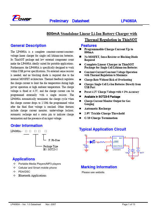
Preliminary Datasheet LP4060AFunctional Pin DescriptionLP4060Pin Number Pin Name Pin FunctionLP4060Note 1: Absolute Maximum Ratings are those values beyond which the life of the device may be impaired. Note 2: The LP4060A are guaranteed to meet performance specifications from 0℃ to 70℃.Specifications over the -40℃ to 85℃ operating temperature range are assured by design,characterization and correlation with statistical process controls.Note 3: See Thermal Considerations.Note 4: Supply current includes PROG pin current (approximately 100µA) but does not include any current delivered to the battery through the BAT pin (approximately 100mA).Note 5: This parameter is not applicable to the LP4060AX.Note 6: I TERM is expressed as a fraction of measured full charge current with indicated PROG resistor.Preliminary Datasheet LP4060A LP4060LP4060LP4060LP4060LP4060 LP4060LP4060Preliminary Datasheet LP4060ALP4060LP4060LP4060LP4060 LP4060LP4060Preliminary Datasheet LP4060APreliminary Datasheet LP4060Aworst-case conditions. ThinSOT powerApplication InformationStability ConsiderationsThe constant-voltage mode feedback loop is stablewithout an output capacitor provided a battery isconnected to the charger output. With no batterypresent, an output capacitor is recommended to reducePreliminary Datasheet LP4060A Average, rather than instantaneous, charge current mayPower DissipationThe conditions that cause the LP4060A to reduce charge current through thermal feedback can be Using the previous example with an ambient Moreover, when thermal feedback reduces the chargePreliminary Datasheet LP4060ABy dropping voltage across a resistor in series with aSolving for I BAT using the quadratic formaulaUsing RCC = 0.25Ω, VS = 5V, VBAT = 3.75V,TA = 25℃and θJA = 125℃/W we can calculate thethermally regulated charge current to be:To detect when the LP4060A is in charge mode, force thedigital output pin (OUT) high and measure the voltage atPreliminary Datasheet LP4060ALP4060USB and Wall Adapter PowerThe LP4060A allows charging from both a wall adapter and aUSB port. Figure 12 shows an example of how to combinewall adapter and USB power inputs. A P-channel MOSFET,Follow the PCB layout guidelines for optimal performance of LP4060A.Preliminary Datasheet LP4060ASOT23-5LP4060A – Ver. 1.0 Datasheet Nov.-2007 Page 13 of 13。
爱司凯ctp制版机说明书
爱司凯ctp制版机说明书型号
T256-8/F3
T256-8/F4
T256-6/F4
T256-6/F5
曝光方式
外鼓式
成像系统
825nm激光
35张/小时
45张/小时
55张/小时
42张/小时
56张/小时
72张/小时
出版能力
1,030×800毫米,版材敏感度100mJ/cm2 780×660毫米,版材敏感度100mJ/cm2
印版尺寸
1,163×940毫米,最小400×300毫米
800×660毫米,最小300×300毫米
版材厚度
0.15毫米-0.3毫米
解像度
2,400dpi或1,200dpi可选2,540dpi或1,270dpi (可变分辨率选件:最高精度圆周方向可达到12,800dpi)
重复精度
士0.01mm
输出接口
光纤接口
标配单版盒或多版盒(MCL-8)或大容量单版盒
上版方式
单版盒
(PL-8)
装版数量
标配单版盒:100张
(0.27m
100张
多版盒(MCL-8) :100张/盒(共4个版盒)
m版材)
打孔系统
选件:支持5套打孔装置
选件:支持3套打孔装置
标配单版盒一体机净重:1,250千克设备净重
1,000千克
多版盒一体机尺寸净重:1,650千克。
SBR40U60CT;中文规格书,Datasheet资料
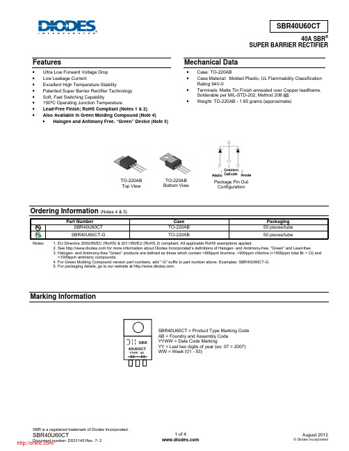
40A SBR ®SUPER BARRIER RECTIFIERFeatures• Ultra Low Forward Voltage Drop • Low Leakage Current • Excellent High Temperature Stability • Patented Super Barrier Rectifier Technology • Soft, Fast Switching Capability • 150ºC Operating Junction Temperature • Lead-Free Finish; RoHS Compliant (Notes 1 & 2) • Also Available in Green Molding Compound (Note 4)• Halogen and Antimony Free. “Green” Device (Note 3)Mechanical Data• Case: TO-220AB • Case Material: Molded Plastic, UL Flammability ClassificationRating 94V-0 • Terminals: Matte Tin Finish annealed over Copper leadframe.Solderable per MIL-STD-202, Method 208 • Weight: TO-220AB - 1.85 grams (approximate)Ordering Information (Notes 4 & 5)Part Number CasePackagingPbSBR40U60CT TO-220AB 50pieces/tubeGreenSBR40U60CT-G TO-220AB50 pieces/tubeNotes:1. EU Directive 2002/95/EC (RoHS) & 2011/65/EU (RoHS 2) compliant. All applicable RoHS exemptions applied.2. See for more information about Diodes Incorporated’s definitions of Halogen- and Antimony-free, "Green" and Lead-free.3. Halogen- and Antimony-free "Green” products are defined as those which contain <900ppm bromine, <900ppm chlorine (<1500ppm total Br + Cl) and <1000ppm antimony compounds.4. For Green Molding Compound version part numbers, add "-G" suffix to part number above. Examples: SBR40U60CT-G.5. For packaging details, go to our website at .Marking InformationPackage Pin Out ConfigurationTO-220ABTop View TO-220AB Bottom ViewSBR40U60CT = Product Type Marking Code AB = Foundry and Assembly Code YYWW = Date Code MarkingYY = Last two digits of year (ex: 07 = 2007) WW = Week (01 - 53)40U60CTMaximum Ratings (Per Leg) (@T A = +25°C, unless otherwise specified.)Single phase, half wave, 60Hz, resistive or inductive load. For capacitance load, derate current by 20%.Characteristic Symbol Value UnitPeak Repetitive Reverse VoltageWorking Peak Reverse Voltage DC Blocking Voltage V RRM V RWMV RM 60 V Average Rectified Output Current (Per Leg) (Total) I O2040 A Non-Repetitive Peak Forward Surge Current 8.3mSSingle Half Sine-Wave Superimposed on rated load I FSM280 AThermal Characteristics (Per Leg)Characteristic Symbol Value UnitTypical Thermal Resistance, Junction to Case R θJC2 ºC/W Operating and Storage Temperature Range T J , T STG-65 to +150 ºCElectrical Characteristics (Per Leg) (@T A = +25°C, unless otherwise specified.)Characteristic Symbol Min Typ Max Unit Test ConditionForward Voltage Drop (per leg) V F- 0.55 0.54 0.600.57 V I F = 20A, T J = 25ºC I F = 20A, T J = 125ºCLeakage Current (Note 6) I R- 0.07 15 0.5100 mA V R = 60V, T J = 25ºC V R = 60V, T J = 125ºCNotes:6. Short duration pulse test used to minimize self-heating effect.Figure1 Typical Forward CharacteristicsV , INSTANTANEOUS FORWARD VOLTAGE (V)F I , I N S T A N T A N E O U S F O R W A R D C U R R EN T (A )F Figure 2 Typical Reverse CharacteristicsV , INSTANTANEOUS REVERSE VOLTAGE (V)R I , I N S T A N T A N E O U S R E V E R S E C U R R E N T (m A )RFigure 4 Operating Temperature Derating5060708090110R T , D E R A T E D A M B I E N T T E M P E R A T U R E (°C )APackage Outline DimensionsPlease see AP02002 at /datasheets/ap02002.pdf for latest version.TO-220ABDim Min Typ Max A 3.56- 4.82 A10.51- 1.39 A2 2.04- 2.92 b 0.390.81 1.01 b2 1.15 1.24 1.77 c 0.356- 0.61 D 14.22- 16.51 D1 8.39- 9.01 e 2.54 e1 5.08 E 9.66- 10.66 H1 5.85- 6.85 L 12.70- 14.73 L1 - -6.35 P 3.54- 4.08 Q 2.54- 3.42 All Dimensions in mmIMPORTANT NOTICEDIODES INCORPORATED MAKES NO WARRANTY OF ANY KIND, EXPRESS OR IMPLIED, WITH REGARDS TO THIS DOCUMENT, INCLUDING, BUT NOT LIMITED TO, THE IMPLIED WARRANTIES OF MERCHANTABILITY AND FITNESS FOR A PARTICULAR PURPOSE (AND THEIR EQUIVALENTS UNDER THE LAWS OF ANY JURISDICTION).Diodes Incorporated and its subsidiaries reserve the right to make modifications, enhancements, improvements, corrections or other changes without further notice to this document and any product described herein. Diodes Incorporated does not assume any liability arising out of the application or use of this document or any product described herein; neither does Diodes Incorporated convey any license under its patent or trademark rights, nor the rights of others. Any Customer or user of this document or products described herein in such applications shall assume all risks of such use and will agree to hold Diodes Incorporated and all the companies whose products are represented on Diodes Incorporated website, harmless against all damages.Diodes Incorporated does not warrant or accept any liability whatsoever in respect of any products purchased through unauthorized sales channel. Should Customers purchase or use Diodes Incorporated products for any unintended or unauthorized application, Customers shall indemnify and hold Diodes Incorporated and its representatives harmless against all claims, damages, expenses, and attorney fees arising out of, directly or indirectly, any claim of personal injury or death associated with such unintended or unauthorized application.Products described herein may be covered by one or more United States, international or foreign patents pending. Product names and markings noted herein may also be covered by one or more United States, international or foreign trademarks.LIFE SUPPORTDiodes Incorporated products are specifically not authorized for use as critical components in life support devices or systems without the express written approval of the Chief Executive Officer of Diodes Incorporated. As used herein:A. Life support devices or systems are devices or systems which:1. are intended to implant into the body, or2. support or sustain life and whose failure to perform when properly used in accordance with instructions for use provided in thelabeling can be reasonably expected to result in significant injury to the user.B. A critical component is any component in a life support device or system whose failure to perform can be reasonably expected to cause thefailure of the life support device or to affect its safety or effectiveness.Customers represent that they have all necessary expertise in the safety and regulatory ramifications of their life support devices or systems, and acknowledge and agree that they are solely responsible for all legal, regulatory and safety-related requirements concerning their products and any use of Diodes Incorporated products in such safety-critical, life support devices or systems, notwithstanding any devices- or systems-related information or support that may be provided by Diodes Incorporated. Further, Customers must fully indemnify Diodes Incorporated and its representatives against any damages arising out of the use of Diodes Incorporated products in such safety-critical, life support devices or systems.Copyright © 2012, Diodes Incorporated分销商库存信息: DIODESSBR40U60CT。
MBR40L60CT 40A 60V肖特基
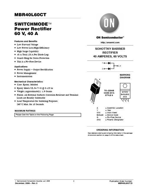
MBR40L60CT SWITCHMODE™Power Rectifier 60 V, 40 AFeatures and Benefits•Low Forward V oltage•Low Power Loss/High Efficiency •High Surge Capability•40 A Total (20 A Per Diode Leg)•Guard−Ring for Stress Protection •This is a Pb−Free Device Applications•Power Supply − Output Rectification •Power Management •InstrumentationMechanical Characteristics:•Case: Epoxy, Molded•Epoxy Meets UL 94 V−0 @ 0.125 in•Weight (Approximately): 1.9 Grams•Finish: All External Surfaces Corrosion Resistant and Terminal Leads are Readily Solderable•Lead Temperature for Soldering Purposes:260°C Max. for 10 SecondsMAXIMUM RATINGSPlease See the Table on the Following PageTO−220ABCASE 221ASTYLE 6SCHOTTKY BARRIERRECTIFIER40 AMPERES, 60 VOLTS13MARKINGDIAGRAM A= Assembly LocationY= YearWW= Work WeekB40L60= Device CodeG= Pb−Free DeviceAKA= Polarity DesignatorSee detailed ordering and shipping information in the package dimensions section on page 2 of this data sheet.ORDERING INFORMATIONMAXIMUM RATINGS (Per Diode Leg)Rating Symbol Value UnitPeak Repetitive Reverse Voltage Working Peak Reverse Voltage DC Blocking Voltage V RRMV RWMV R60VAverage Rectified Forward Current(Per Leg) (Rated V R) T C = 130°C(Per Device)I F(AV)2040ANonrepetitive Peak Surge Current(Surge applied at rated load conditions halfwave, single phase, 60 Hz)I FSM240A Operating Junction Temperature (Note 1)T J−55 to +150°C Storage Temperature T stg−65 to +175°CESD Ratings:Machine Model = CHuman Body Model = 3B > 400> 8000VTHERMAL CHARACTERISTICSRating Symbol Value UnitMaximum Thermal Resistance− Junction−to−Case− Junction−to−Ambient R q JCR q JA1.870°C/WELECTRICAL CHARACTERISTICS (Per Diode Leg)Rating Symbol Typ Max UnitMaximum Instantaneous Forward Voltage (Note 2)(I F = 20 A, T C = 25°C)(I F = 20 A, T C = 125°C)(I F = 40 A, T C = 25°C)(I F = 40 A, T C = 125°C)v F0.560.530.750.690.610.580.810.74VMaximum Instantaneous Reverse Current (Note 2)(Rated DC Voltage, T C = 25°C)(Rated DC Voltage, T C = 125°C)i R21095550175m AmAStresses exceeding Maximum Ratings may damage the device. Maximum Ratings are stress ratings only. Functional operation above the Recommended Operating Conditions is not implied. Extended exposure to stresses above the Recommended Operating Conditions may affect device reliability.1.The heat generated must be less than the thermal conductivity from Junction−to−Ambient: dP D/dT J < 1/R q JA.2.Pulse Test: Pulse Width = 300 m s, Duty Cycle ≤2.0%.DEVICE ORDERING INFORMATIONDevice Order Number Package Type Shipping†MBR40L60CTG TO−220AB(Pb−Free)50 Units / Rail†For information on tape and reel specifications, including part orientation and tape sizes, please refer to our Tape and Reel Packaging Specification Brochure, BRD8011/D.I F , I N S T A N T A N E O U S F O R W A R D C U R R E N T (A )V F , INSTANTANEOUS FORWARD VOLTAGE (V)Figure 1. Typical Forward VoltageV F , INSTANTANEOUS FORWARD VOLTAGE (V)Figure 2. Maximum Forward VoltageI F , A V E R A G E F O R W A R D C U R R E N T (A )1.0E −1.0E −1.0E −1.0E −1.0E −1.0E −V R , REVERSE VOLTAGE (V)Figure 3. Typical Reverse CurrentI R , R E V E R S E C U R R E N T (A )1.0E −1.0E −1.0E −1.0E −1.0E −1.0E −V R , REVERSE VOLTAGE (V)Figure 4. Maximum Reverse CurrentR I F , A V E R A G E F O R W A R D CU R R E N T (A )T C , CASE TEMPERATURE (°C)Figure 5. Current Derating, Case per Leg I F , A V E R A G E F O R W A R D C U R R E N T (A )T A , AMBIENT TEMPERATURE (°C)Figure 6. Current Derating, Ambient per LegP F , A V E R A G E P O W E R D I S S I P A T I O N (W )I O , AVERAGE FORWARD CURRENT (A)Figure 7. Forward Power Dissipation10100100010000V R , REVERSE VOLTAGE (V)Figure 8. CapacitanceC , C A P A C I T A N C E (p F )0.010.11100.0000010.000010.00010.0010.010.11101001000R (t ), T R A N S I E N T T H E R M A L R E S I S TA N C EFigure 9. Thermal Response Junction −to −Case for MBR40L60CTt 1, TIME (sec)R (t ), T R A N S I E N T T H E R M A L R E S I S T A N C EFigure 10. Thermal Response Junction −to −Ambient for MBR40L60CTPULSE TIME (sec)PACKAGE DIMENSIONSTO −220CASE 221A −09ISSUE AFNOTES:1.DIMENSIONING AND TOLERANCING PER ANSI Y14.5M, 1982.2.CONTROLLING DIMENSION: INCH.3.DIMENSION Z DEFINES A ZONE WHERE ALL BODY AND LEAD IRREGULARITIES ARE ALLOWED.STYLE 6:PIN 1.ANODE 2.CATHODE 3.ANODE 4.CATHODEDIM MIN MAX MIN MAX MILLIMETERS INCHES A 0.5700.62014.4815.75B 0.3800.4059.6610.28C 0.1600.190 4.07 4.82D 0.0250.0350.640.88F 0.1420.161 3.61 4.09G 0.0950.105 2.42 2.66H 0.1100.155 2.80 3.93J 0.0140.0250.360.64K 0.5000.56212.7014.27L 0.0450.060 1.15 1.52N 0.1900.210 4.83 5.33Q 0.1000.120 2.54 3.04R 0.0800.110 2.04 2.79S 0.0450.055 1.15 1.39T 0.2350.255 5.97 6.47U 0.0000.0500.00 1.27V 0.045--- 1.15---Z---0.080--- 2.04FSEATINGPLANEON Semiconductor and are registered trademarks of Semiconductor Components Industries, LLC (SCILLC). SCILLC reserves the right to make changes without further notice to any products herein. SCILLC makes no warranty, representation or guarantee regarding the suitability of its products for any particular purpose, nor does SCILLC assume any liability arising out of the application or use of any product or circuit, and specifically disclaims any and all liability, including without limitation special, consequential or incidental damages.“Typical” parameters which may be provided in SCILLC data sheets and/or specifications can and do vary in different applications and actual performance may vary over time. All operating parameters, including “Typicals” must be validated for each customer application by customer’s technical experts. SCILLC does not convey any license under its patent rights nor the rights of others. SCILLC products are not designed, intended, or authorized for use as components in systems intended for surgical implant into the body, or other applications intended to support or sustain life, or for any other application in which the failure of the SCILLC product could create a situation where personal injury or death may occur.Should Buyer purchase or use SCILLC products for any such unintended or unauthorized application, Buyer shall indemnify and hold SCILLC and its officers, employees, subsidiaries,affiliates, and distributors harmless against all claims, costs, damages, and expenses, and reasonable attorney fees arising out of, directly or indirectly, any claim of personal injury or death associated with such unintended or unauthorized use, even if such claim alleges that SCILLC was negligent regarding the design or manufacture of the part. SCILLC is an Equal Opportunity/Affirmative Action Employer. This literature is subject to all applicable copyright laws and is not for resale in any manner.PUBLICATION ORDERING INFORMATIONSWITCHMODE is a trademark of Semiconductor Components Industries, LLC.。
铂纳特斯产品详细资料
铂纳特斯产品详细资料功用特点:1.公用于原柱锂离子电池注液;2.采样先抽真空后注液,注液后真空,压力交替停止的静置方式;3.效率高,精度高,操作方便牢靠;4.抽真空时间、静置时间可依据状况设定,可选加压静置或常压静置;5.注液精度为±0.1g ,注液量要求为可调;6.注液时真空压力:坚持在-98KPa以上。
任务效率:25~30PPM〔18650〕;7.适用于18650、26650或相似硬壳电池、方型铝壳电池、电容自动注液;8. 全自动智能化管理系统,具有自动挑选不合格的产品功用.铂纳特斯26650和18650全自动注液机功用特点:1.先真空后注液工艺方式,电解液吸收分歧性、牢靠性、完全性高;2.适用于18650、26650或相似硬壳电池、电容自动注液;3.该结构也适用于∮1.2~1.4mm小注液口硬壳电池、电容自动注液;4.效率:60PPM或30PPM两种 (18650);5.电池注液量精度:18650 为+-0.1g;6.全自动智能化管理系统,具有自动挑选不合格的产品功用;7.专业设计, 维护简易。
动力电池:铂纳特斯动力电池注液机:功用特点:1.注液精度为±0.1g ,注液量要求为可调;2.自动化水平高,可按客户要求带有自动清洗系统;3.远程调试系统,注液量注液精度完成智能化管理;4.适用于各类硬壳电池、电容自动注液;5.全自动智能化管理系统,具有自动挑选不合格的产品功用;6.效率高,精度高,操作方便牢靠,维护简易。
注液机控制箱功用特点:1.全触摸屏控制;2.采用出口可编程控制器,电脑、人机界面控制;3.采用高功用、高分辨率、触摸屏控制,可操作性强;4.全部采用出口电器元器件;5.智能管理系统,设备形状实时显示;6.操作方便牢靠,专业设计,维护简易。
运转图:注液机控制箱触摸屏显示图:全自动注液机消费线:动力电池手套注液机:功用特点:1、适用于环型、方型及圆型硬壳电池;2、先真空后注液工艺方式,电解液吸收分歧性、牢靠性、完全性高;3、可配全自动上下料流水线;4、可在手套箱和枯燥房里操作;5、全自动智能化管理系统,具有自动挑选不合格的产品功用;6、专业设计, 维护简易。
- 1、下载文档前请自行甄别文档内容的完整性,平台不提供额外的编辑、内容补充、找答案等附加服务。
- 2、"仅部分预览"的文档,不可在线预览部分如存在完整性等问题,可反馈申请退款(可完整预览的文档不适用该条件!)。
- 3、如文档侵犯您的权益,请联系客服反馈,我们会尽快为您处理(人工客服工作时间:9:00-18:30)。
40A SBRSUPER BARRIER RECTIFIERFeatures• Low Forward Voltage Drop• Excellent High Temperature Stability• Patented Super Barrier Rectifier Technology • Soft, Fast Switching Capability• Lead-Free Finish; RoHS Compliant (Notes 1 & 2) • Also Available in Green Molding Compound • Halogen and Antimony Free. “Green” Device (Note 3)Mechanical Data•Case: TO-220AB, ITO-220AB• Case Material: Molded Plastic, UL Flammability Classification Rating 94V-0• Terminals: Matte Tin Finish annealed over Copper leadframe.Solderable per MIL-STD-202, Method 208 • Weight: TO-220AB – 1.85 grams (approximate)ITO-220AB – 1.65 grams (approximate)Ordering Information (Notes 4 and 5)Part Number CasePackagingPbSBR4060CT TO-220AB 50pieces/tubeGreenSBR4060CT-G TO-220AB 50pieces/tubePbSBR4060CTFP ITO-220AB 50 pieces/tube GreenSBR4060CTFP-G ITO-220AB 50 pieces/tubePbSBR4060CTFP-JT ITO-220AB(Alternate)50 pieces/tubeNotes:1. EU Directive 2002/95/EC (RoHS) & 2011/65/EU (RoHS 2) compliant. All applicable RoHS exemptions applied.2. See for more information about Diodes Incorporated’s definitions of Halogen- and Antimony-free, "Green" and Lead-free.3. Halogen- and Antimony-free "Green” products are defined as those which contain <900ppm bromine, <900ppm chlorine (<1500ppm total Br + Cl) and <1000ppm antimony compounds.4. For Green Molding Compound version part numbers, add "-G" suffix to part number above. Examples: SBR4060CT-G.5. For packaging details, go to our website at .Marking InformationTO-220AB Top View ITO-220AB Top View Package Pin Out ConfigurationTO-220AB Bottom View ITO-220AB Bottom ViewSBR4060CTFP = Product Type Marking Code AB = Foundry and Assembly Code YYWW = Date Code MarkingYY = Last two digits of year (ex: 06 = 2006) WW = Week (01 - 53)SBR4060CT = Product Type Marking Code AB = Foundry and Assembly Code YYWW = Date Code MarkingYY = Last two digits of year (ex: 06 = 2006) WW = Week (01 - 53)SBR4060CTFP YYWW ABSBR4060CT YYWWABMaximum Ratings (Per Leg) @T A = 25°C unless otherwise specifiedSingle phase, half wave, 60Hz, resistive or inductive load. For capacitance load, derate current by 20%.Characteristic Symbol Value UnitPeak Repetitive Reverse VoltageWorking Peak Reverse Voltage DC Blocking Voltage V RRM V RWMV RM 60 V Average Rectified Output Current Per Device (Per Leg) (Total) I O2040 A Non-Repetitive Peak Forward Surge Current 8.3msSingle Half Sine-Wave Superimposed on Rated Load I FSM280 A Peak Repetitive Reverse Surge Current (2uS-1Khz) I RRM 2 A Isolation Voltage (ITO-220AB Only)From terminal to heatsink t = 3 sec. V AC2000 VThermal Characteristics (Per Leg)Characteristic Symbol Value UnitTypical Thermal ResistancePackage = TO-220AB Package = ITO-220ABR θJC2 4 ºC/W Operating and Storage Temperature Range T J , T STG -65 to +150 ºCElectrical Characteristics (Per Leg) @T A = 25°C unless otherwise specifiedCharacteristic Symbol Min Typ Max Unit TestConditionForward Voltage Drop V F- - 0.61 0.700.65 V I F = 20A, T J = 25ºC I F = 20A, T J = 125ºCLeakage Current (Note 6) I R- - 0.5100 mA V R = 60V, T J = 25ºC V R = 60V, T J = 125ºCNotes:6. Short duration pulse test used to minimize self-heating effect.7. Using heatsink (by Black Aluminum 37mm*50mm*15mm)Fig. 1 Forward Power DissipationI , AVERAGE FORWARD CURRENT (A)F(AV)P ,P O W E R D I S S I P A T I O N (W )D V , INSTANTANEOUS FORWARD VOLTAGE (V)Fig. 2 Typical Forward CharacteristicsF I , I N S T A N T A N E O U S F O R W A R D C U R R E N T (A )FFig. 3 Typical Reverse CharacteristicsV , INSTANTANEOUS REVERSE VOLTAGE (V)R I , I N S T A N T A N E O U S R E V E R S E C U R R E N T (µA )R Fig. 4 Forward Current Derating CurveT , AMBIENT TEMPERATURE (C)A °I , A V E R A G E F O R W A R D C U R R E N T (A )F (A V)Fig. 5 Operating T emperature DeratingV , DC REVERSE VOLTAGE (V)R T ,D E R A T E D A M B I E N T T E M P E R A T U R E (C )A °Package Outline DimensionsNotes: 8. For product manufactured with Date Code 0733 (week 33, 2007) and newer, please refer to ITO-220AB dimensions. For product manufactured prior to Date Code 0733, please refer to ITO-220AB ALTERNATE dimensions.ITO-220AB(Note 8)Dim Min Typ Max A 4.50 4.70 4.90A1 3.04 3.24 3.44A2 2.56 2.762.96b 0.500.600.75b1 1.10 1.20 1.35c 0.500.600.70D 15.6715.8716.07D1 8.999.199.39e 2.54E 9.9110.1110.31L 9.459.7510.05L1 15.8016.0016.20P 2.98 3.18 3.38Q 3.10 3.30 3.50All Dimensions in mmTO-220ABDim Min Typ Max A 3.56- 4.82A1 0.51- 1.39A2 2.04- 2.92b 0.390.81 1.01b2 1.15 1.24 1.77c 0.356- 0.61D 14.22- 16.51D1 8.39- 9.01e 2.54 e1 5.08 E 9.66- 10.66H1 5.85- 6.85L 12.70- 14.73L1 - - 6.35P 3.54- 4.08Q 2.54- 3.42All Dimensions in mmITO-220AB Alternate (Note 8)Dim Min MaxA 4.36 4.77 A1 2.54 3.1 A2 2.54 2.8 b 0.55 0.75 b1 1.2 1.5 c 0.38 0.68 D 14.5 15.5 D1 8.38 8.89 E 9.72 10.27 e 2.41 2.67 L 9.87 10.67 L1 15.8 17 ØP 3.08 3.39 Q 2.6 3.0 All Dimensions in mmIMPORTANT NOTICEDIODES INCORPORATED MAKES NO WARRANTY OF ANY KIND, EXPRESS OR IMPLIED, WITH REGARDS TO THIS DOCUMENT, INCLUDING, BUT NOT LIMITED TO, THE IMPLIED WARRANTIES OF MERCHANTABILITY AND FITNESS FOR A PARTICULAR PURPOSE (AND THEIR EQUIVALENTS UNDER THE LAWS OF ANY JURISDICTION).Diodes Incorporated and its subsidiaries reserve the right to make modifications, enhancements, improvements, corrections or other changes without further notice to this document and any product described herein. Diodes Incorporated does not assume any liability arising out of the application or use of this document or any product described herein; neither does Diodes Incorporated convey any license under its patent or trademark rights, nor the rights of others. Any Customer or user of this document or products described herein in such applications shall assume all risks of such use and will agree to hold Diodes Incorporated and all the companies whose products are represented on Diodes Incorporated website, harmless against all damages.Diodes Incorporated does not warrant or accept any liability whatsoever in respect of any products purchased through unauthorized sales channel. Should Customers purchase or use Diodes Incorporated products for any unintended or unauthorized application, Customers shall indemnify and hold Diodes Incorporated and its representatives harmless against all claims, damages, expenses, and attorney fees arising out of, directly or indirectly, any claim of personal injury or death associated with such unintended or unauthorized application.Products described herein may be covered by one or more United States, international or foreign patents pending. Product names and markings noted herein may also be covered by one or more United States, international or foreign trademarks.LIFE SUPPORTDiodes Incorporated products are specifically not authorized for use as critical components in life support devices or systems without the express written approval of the Chief Executive Officer of Diodes Incorporated. As used herein:A. Life support devices or systems are devices or systems which:1. are intended to implant into the body, or2. support or sustain life and whose failure to perform when properly used in accordance with instructions for use provided in thelabeling can be reasonably expected to result in significant injury to the user.B. A critical component is any component in a life support device or system whose failure to perform can be reasonably expected to cause thefailure of the life support device or to affect its safety or effectiveness.Customers represent that they have all necessary expertise in the safety and regulatory ramifications of their life support devices or systems, and acknowledge and agree that they are solely responsible for all legal, regulatory and safety-related requirements concerning their products and any use of Diodes Incorporated products in such safety-critical, life support devices or systems, notwithstanding any devices- or systems-related information or support that may be provided by Diodes Incorporated. Further, Customers must fully indemnify Diodes Incorporated and its representatives against any damages arising out of the use of Diodes Incorporated products in such safety-critical, life support devices or systems.Copyright © 2012, Diodes Incorporated分销商库存信息:DIODESSBR4060CTFP SBR4060CT。