电容电感表dm6243集成块资料大全
TLE6244中文资料
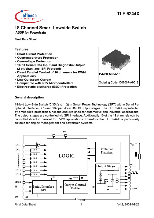
VS
IN1 IN2
IN15 IN16 SCLK SI
as Ch. 1 as Ch. 1 as Ch. 1 as Ch. 1 as Ch. 1 as Ch. 1 as Ch. 1
LOGIC
16
1
16
Serial Interface SPI
Output Control Buffer
SO
Final Data Sheet
OUT2 OUT3 OUT4 OUT5 OUT6 OUT7 OUT8 OUT9 OUT10 OUT11 OUT12 OUT13 OUT14 OUT15 OUT16 OUT17 OUT18
VDD VDD-Moni-
toring
GND_ABE
VDD ABE
Final Data Sheet
3
V4.2, 2003-08-29
元器件交易网
TLE 6244X
1.3 Description of the Power Stages
OUT1... OUT6
6 non-inverting low side power switches for nominal currents up to 2.2A. Control is possible by input pins, by the µsec-bus or via SPI. For TJ = 25°C the on-resistance of the power switches is below 400mΩ. An integrated zener diode limits the output voltage to 70V typically.
A protection for inverse current is implemented for OUT1... OUT4 for use as stepper-motor control.
万用表

VC60D
3 1/2位兆欧表:电压量程:1000V/2500V,电阻量程:200MΩ/2GΩ/20GΩ
950
VC60E
3 1/2位兆欧表:电压量程:2500V/5000V,电阻量程:2GΩ/20GΩ/200GΩ
1600
台式万用表
VC8045-Ⅱ
4 1/2位真有效值台式数字万用表(0.05%),(V,A,Ω,C,Hz)交流频响50Hz-50kHz,二,三极管测量,通断报警,220V供电,背光显示
140
VC10C+
3 3/4万用表(V,A,Ω,℃,200uF,30MHz)自动关机,自动量程,电压/频率/占空比,相对值测量,数据保持,符号显示,全功能保护
210
VC96A
3 3/4自动量程(V,A,Ω,,200uF,30MHz)二极管测试,通断报警,低电压显示,自动关机,功能保护,防震保护,电池测量,AC频响40-400Hz
4600
VICTOR05
5位(0.05%)校验仪,输出:电流:0~22mA,模拟变送器:0~-22mA,回路电源:24V,输入,电压:0~28V,电流:0~22mA,回路电流:0~22mA
4800
温度探头
TP01
标准K型温度探头250℃
10
TP02
标准K型温度探头750℃
20
TP03
标准K型温度探头1300℃
1999位,大屏幕,保护套,有通断蜂鸣,电容,温度,二级管,数据保持,背光,自动关机
优利德
175
UT50C数字万用表
1999位,大屏幕,保护套,有通断蜂鸣,电容,温度,频率,二级管,数据保持,背光,自动关机
4600
VICTOR03
贴片电感标示

电感值 Inductance hnHi
1.0M0.3nH 1.2M0.3nH 1.5M0.3nH 1.8M0.3nH 2.0M0.3nH 2.2M0.3nH 2.4M0.3nH 2.7M0.3nH 3.0M0.3nH 3.3M0.3nH 3.6M0.3nH 3.9M0.3nH 4.3M0.3nH 4.7M0.3nH 5.1M0.3nH 5.6M0.3nH 6.2M0.3nH 6.8M5% 7.5M5% 8.2M5% 9.1M5% 10M5% 12M5% 15M5% 18M5% 22M5% 27M5% 33M5% 39M5% 47M5% 56M5% 68M5% 82M5% 100M5% 120M5%
自共振频率 直流电阻 额定电流 Self-resonant DC.Resistance Rated frequency current hEi [MHz] hmAi 1000 min. Typ. max. Typ. max.
27 25 23 23 22 22 22 22 21 21 20 19 18 18 17 17 16 15 14 12 11 10 10 8 6 10000 X13000 10000 X13000 10000 X13000 10000 X13000 8800 12500 7700 11000 6700 9600 6000 8600 5300 7600 4600 6600 3900 5600 3400 4900 2900 4200 2700 3800 2300 3300 2100 3000 1800 2600 1800 2600 1700 2400 1500 2100 1300 1800 1100 1600 1100 1500 1000 1400 900 1200 0.14 0.088 0.14 0.089 0.18 0.11 0.19 0.12 0.22 0.14 0.25 0.16 0.3 0.19 0.3 0.2 0.4 0.25 0.4 0.25 0.48 0.3 0.55 0.34 0.63 0.39 0.7 0.45 0.8 0.5 0.9 0.57 1.2 0.71 1.8 1.11 2.1 1.33 2.4 1.51 2.8 1.74 3.0 1.85 3.0 2.30 3.5 2.60 4.0 3.00 250 250 230 200 200 200 180 170 150 150 150 150 150 100 100 100 100 50 50 50 50 50 50 50 40
TPIC6273中文资料
元器件交易网IMPORTANT NOTICETexas Instruments and its subsidiaries (TI) reserve the right to make changes to their products or to discontinueany product or service without notice, and advise customers to obtain the latest version of relevant informationto verify, before placing orders, that information being relied on is current and complete. All products are soldsubject to the terms and conditions of sale supplied at the time of order acknowledgement, including thosepertaining to warranty, patent infringement, and limitation of liability.TI warrants performance of its semiconductor products to the specifications applicable at the time of sale inaccordance with TI’s standard warranty. Testing and other quality control techniques are utilized to the extentTI deems necessary to support this warranty. Specific testing of all parameters of each device is not necessarilyperformed, except those mandated by government requirements.CERTAIN APPLICATIONS USING SEMICONDUCTOR PRODUCTS MAY INVOLVE POTENTIAL RISKS OFDEATH, PERSONAL INJURY, OR SEVERE PROPERTY OR ENVIRONMENTAL DAMAGE (“CRITICALAPPLICATIONS”). TI SEMICONDUCTOR PRODUCTS ARE NOT DESIGNED, AUTHORIZED, ORWARRANTED TO BE SUITABLE FOR USE IN LIFE-SUPPORT DEVICES OR SYSTEMS OR OTHERCRITICAL APPLICATIONS. INCLUSION OF TI PRODUCTS IN SUCH APPLICATIONS IS UNDERSTOOD TOBE FULLY AT THE CUSTOMER’S RISK.In order to minimize risks associated with the customer’s applications, adequate design and operatingsafeguards must be provided by the customer to minimize inherent or procedural hazards.TI assumes no liability for applications assistance or customer product design. TI does not warrant or representthat any license, either express or implied, is granted under any patent right, copyright, mask work right, or otherintellectual property right of TI covering or relating to any combination, machine, or process in which suchsemiconductor products or services might be or are used. TI’s publication of information regarding any thirdparty’s products or services does not constitute TI’s approval, warranty or endorsement thereof.Copyright © 1998, Texas Instruments Incorporated。
L6234中文资料

Commutation Frequency
Reference Voltage
Total Power Dissipation
L6234PD Tamb = 70°C
Total Power Dissipation
L6234 Tamb = 70°C
Storage and Junction Temperature Range
Application Note AN467: Thermal Characteristics of the PowerDip 20,24 Packages Soldered on 1,2,3 oz. Copper PCB
Application Note AN668: A New High Power IC Surface Mount Package: PowerSO20 Power IC Packaging from Insertion to Surface Mounting.
POWER DIP (16+2+2) PowerSO20
DESCRIPTION The L6234 is a triple half bridge to drive a brushless motor. It is realized in Multipower BCD technology which combines isolated DMOS power transistors with CMOS and Bipolar circuits on the same chip. By using mixed technology it has been possible to optimize the logic circuitry and the power stage to achieve the best possible performance. The output DMOS transistors can sustain a very high current due to the fact that the DMOS structure is not affected by the second breakdown ef-
BUF634中文资料
目录产品特点: (2)应用: (2)描述: (2)规格: (3)引脚结构: (5)绝对最大额定值: (5)典型性能曲线:在T A = 25°C,V S =±15V,除非另有说明。
(6)应用信息: (9)输出电流: (9)热保护: (9)功耗: (10)输入特性: (10)带宽控制PIN: (10)提高运算放大器的输出电流: (10)高频应用: (11)封装形式 (14)产品特点:●高输出电流:250mA●转换速度:2000 v / μs●PIN所选带宽:30MHz到180MHz●低静态电流:1.5mA(30MHz的带宽)●电源范围:±2.25〜±18V●内部电流可限制●过热关断保护●8引脚DIP,SO-8,5引脚TO-220,5引脚DDPAK表面贴装应用:●阀驱动●电磁驱动器●运算放大器电流升压●线路驱动器●耳机驱动器●视频驱动程序●电机驱动器●测试设备●ATE引脚驱动器描述:BUF634是一种高速开环单位增益缓冲器,适用范围广的应用中建议。
它可用于运算放大器的反馈环路内,以增加输出电流,消除热反馈,并提高容性负载驱动。
对于低功耗应用,BUF634静态电流1.5mA具有250mA输出,2000V/μs摆率和30MHz 带宽。
V-和BW引脚之间连接一个电阻,可以调整带宽从30MHz到180MHz。
输出电路完全由内部电流限制和热关断,使其坚固耐用和易于使用的保护。
BUF634可在多种封装形式,以适应机械和功耗要求。
类型包括8引脚DIP,SO-8表面贴装,5引脚TO-220,采用5引脚DDPAK表面贴装塑料功率封装。
规格:(在T A = 25°C ,V S =±15V ,除非另有说明)引脚结构:绝对最大额定值:供应电压................................................ ..................................... ±18V 输入电压范围............................................... ................................ ±V S 输出短路(接地).......................................... .......连续工作温度................................................ ..... -40°C至125°C储存温度................................................ ........ -55°C至125°C结温................................................ ....................... 150°C铅温度(焊接,10s)........................................... ......... 300°C典型性能曲线:在T A = 25°C,V S =±15V,除非另有说明。
电容感性负载驱动——超声功率放大器 功率放大器常见问题解决方法

电容感性负载驱动——超声功率放大器功率放大器常见问题解决方法随着电子试验室的测试讨论升级,很多试验测试都需要用到信号源、示波器、超声功率放大器等测试仪器,压电陶瓷晶片是一种结构简单且灵活的电学器件,当电压作用于压电陶瓷时,就会随电压和频率的变化产生机械变形;在很多测试中驱动都需要高电压、大功率。
电容性负载驱动:压电器件电压放大器当振动压电陶瓷时,则会产生相应电荷。
压电陶瓷晶片适合机械形变、振动、次声波、声波和超声波和次声波的产生和检测,具有灵敏度高,无磁场散播外溢,不用铜线和磁铁,成本低耗电少,便于大量生产等优点而获得了广泛应用。
常见的压电器件包括:压电陶瓷片、压电传感器、压电换能器等。
ATA—2000系列是一款理想的可放大交、直流信号的超声功率放大器。
大差分输出1600Vp—p (800V)高压,可以驱动高压型负载。
电压增益数控可调,一键保存常用设置,为您供应了便利简洁的操作选择,同时双通道高压放大器输出还可同步调整,可与主流的信号发生器配套使用,实现信号的放大。
电感性负载驱动:磁场线圈亥姆霍兹线圈,是指假如有一对相同的载流圆线圈彼此平行且共轴,通以同方向电流,当线圈间距等于线圈半径时,两个载流线圈的总磁场在轴的中点相近的范围内是均匀的。
亥姆霍兹线圈紧要用途是,产生标准磁场;霍尔探头和各种磁强计的定标;地磁场的补偿;磁屏蔽效果的判定;空间辐射磁场的测量和排出;物质磁特性的讨论;生物磁性的讨论等等。
ATA—3000系列功率放大器是一款理想的可放大交、直流信号的功率放大器。
大输出功率810W,可以驱动功率型负载。
电压增益数控可调,一键保存常用设置,为您供应了便利简洁的操作选择,可与主流的信号发生器配套使用,实现信号的放大。
功率放大器原理如何?高频功率放大器用于发射机的末级,作用是将高频已调波信号进行功率放大,以充分发送功率的要求;然后经过天线将其辐射到空间,保证在确定区域内的接收机可以接收到充分的信号电平,并且不干扰相邻信道的通信。
SP6223中文资料

DESCRIPTION■ SMPS Post-Regulator ■ DC-to-DC Modules ■ Medical Devices ■ Data Cable ■ PagersFEATURESAPPLICATIONSThe SP6222 and SP6223 are CMOS LDOs designed to meet a broad range of applications that require accuracy,speed and ease of use. These LDOs offer extremely low quiescent current which only increases slightly under load,thus providing advantages in ground current performance over bipolar LDOs. The LDOs handle an extremely wide load range and guarantee stability with a 1μF ceramic output capacitor. They have excellent low frequency PSRR,not found in other CMOS LDOs and thus offer exceptional Line Regulation. High frequency PSRR is 55dB (typical)at 1kHz. Load Regulation is excellent and temperature stability is comparable to bipolar LDOs. An enable feature is provided on all versions. The SP6222/6223 is available in fixed and adjustable output voltage versions in industry standard SC70 and SOT23 packages.TYPICAL APPLICATION CIRCUITVery low Dropout Voltage: 200mV typ (150mA load) High Output Setpoint Accuracy of 2% Very low Input Voltages Down to 1.6VPower-saving Shutdown Mode of 150nA (typ) Fast Turn-on (90μs) and Turn-off (90μs)Extremely low Quiescent Current of 14μA (typ) Very Tight Line regulation, 0.2%/V Load Regulation 0.125 mV/mA Thermal Shutdown ProtectionLow Noise Output, 100μV RMS With 10nF Bypass Fixed or Adjustable Output Versions AvailableAvailable in RoHS Compliant, Lead Free Packages:SC70 and SOT23■ Cellular Telephones■ Laptop, Notebooks and Palmtop Computers ■ Battery-Powered Equipment ■ Consumer/ Personal Electronics3.0VENABLEELECTRICAL CHARACTERISTICSABSOLUTE MAXIMUM RATINGSThese are stress ratings only and functional operation of the device at these ratings or any other above those indicated in the operation sections of the specifications below is not implied. Exposure to absolute maximum rating conditions for extended periods of time may affect reliability.Storage Temperature...........................-65°C to +150°C Junction Temperature (T J )....................-40°C to +125°C Lead Temperature (soldering 5s).........................300°C Supply Input Voltage (V IN ).............................-2V to 6V Output Voltage (V OUT ).........................-0.6V to V IN +1V Enable Input Voltage (V EN )............................-2V to 7V Power Dissipation (P D )..........Internally Limited, Note 1Unless otherwise specified: V IN = V OUT + 0.3V to 4.5V, C OUT = 1μF ceramic, C IN = 1μF ceramic, I OUT =100μA, T A = 25°C.Bold values apply over the full operating temperature range (-40°C to 125°C).Note 1.The maximum allowable power dissipation at any T A (ambient temperature) is P D (MAX) = (T J (MAX)– T A ) /θJA . Exceeding the maximum allowable power dissipation will result in excessive die temperature, and the regulator will go into thermal shutdown. The θJA of the SP6222/23 (SC-70-5) is 330°C/W mounted on a PC board with minimum copper area (see “Thermal Considerations” section for further details).Note 2.Minimum V IN must meet 2 conditions: V IN >1.6V and V IN > {V OUT + DOV}Note 3.Dropout Voltage DOV is defined as the input to output differential at which the output voltage drops2% below its nominal value measured at 1V differential. The DOV specification is not applicable to output voltages less than 2.7V.ELECTRICAL CHARACTERISTICSUnless otherwise specified: VIN = VOUT+ 0.3V to 4.5V, COUT= 1μF ceramic, CIN= 1μF ceramic, IOUT=100μA, TA= 25°C.Bold values apply over the full operating temperature range (-40°C to 125°C).General OverviewThe SP6222 and SP6223 are CMOS LDOs designed to meet a broad range of low voltage applications that require accuracy and ease of use. The SP6222 offers a 50mA output current while the SP6223 offers an output current of 150mA. The SP6222 is available in a 2.5V or 3.0V fixed output along with an adjustable output version. The SP6223 is offered in an adjustable output only. These LDOs have a minimum input voltage of only 1.6V and a maximum input voltage of 4.5V. The output voltage can be programmed to as low as 0.9V and have a maximum dropout voltage rating of 100mV for the SP6222 and 300mV for the SP6223. Both devices are equipped with an enable (EN) input for very low current (10nA typical) shutdown mode.Enable / Shutdown OperationThe SP6222/6223 is turned on by providing 1.6V or greater to the EN pin. To place the device into shutdown pull the EN pin below 0.4V. If this feature is not required connect EN to input supply to always enable the device whenever power is applied.Input / Output CapacitorThe SP6222/6223 is designed to operate using very small ceramic capacitors. The minimum input and output capacitor value for stable operation is 1.0μF. The output capacitor value may be increased without limit to improve transient response. Place these capacitors as close as possible to the device.Bypass (BYP) CapacitorThe fixed output versions offer a BYP pin to decouple the bandgap reference. Connecting an external 10nF capacitor from BYP to GND can reduce output noise. If output noise is not a concern the BYP pin may be left open. When a bypass capacitor is used the turn on time is slower. See the following turn on time plots for various BYP capacitor values. The adjustable output version does not offer this BYP input. Adjustable RegulatorThe output of the device can be programmed to a specific voltage by using two external resistors connected to the ADJ pin (see Typical Application Circuit for Adjustable output). The resistors set APPLICATION INFORMATIONthe output voltage based on the following equation:V OUT = V REF *(R1/R2 + 1)Resistor values are not critical because the ADJ (adjust) pin has a high impedance, but for best performance use resistor values of 470K Ω or less.Thermal ConsiderationsThe SP6222/6223 is designed to provide 50mA -150mA of continuous current in a tiny package. Maximum power dissipation can be calculated based on the output current and the voltage drop across the part. To determine the maximum power dissipation of the package, use the junction-to-ambient thermal resistance of the device and the following equation:P D(MAX) = (T J(max) – T A ) / θJAT J(max) is the maximum junction temperature of the die and is 125o C.T A is the ambient temperature. θJA is the junction-to-ambient thermal resistance of the package. The SOT-23 package has a θJA of approximately 191o C/W and the SC70 package has a θof approximately 330o C/W.The actual power dissipation of the regulator circuit can be determined by using the simplified equation:P D = (V IN – V OUT ) * I OUTTo prevent the device from entering thermal shutdown, maximum power dissipation cannot be exceeded.Layout ConsiderationsThe primary path of heat conduction out of the package is via the package leads. Therefore, careful consideration must be taken into account for optimizing layout.1.Attaching the part to a large copper footprint will enable better heat transfer from the device, especially where there are internal ground and power planes.2.Place the input and output capacitors close to the device for optimal transient response and device behavior.3.Connect all ground connections directly to the ground plane. In case there is no ground plane,connect to a common ground point before connecting to board ground.APPLICATION INFORMATIONAPPLICATION INFORMATIONVoutIout @ 100mA/divSP6223 1.2Vout fixed Cin = Cout = 1.0uF Cer Iout = 100uA to 150mASP6223 1.2Vout fixed Cin = Cout = 1.0uF Cer Iout = 100uA to 150mAVoutIout @ 100mA/divIout @ 100mA/divSP6223 1.2Vout fixed Cin = Cout = 1.0uF Cer Iout = 100uA to 100mAVoutSP6223 1.2Vout fixed Cin = Cout = 1.0uF Cer Iout = 100uA to 100mAVoutLoad Transient Response, 100μA to 150mA,Vin = 1.6VLoad Transient Response, 100Vin = 3.3VLoad Transient Response, 100Vin = 1.6VLoad Transient Response, 100Vin = 3.3VAPPLICATION INFORMATIONIout @ 100mA/divSP6223 1.2Vout fixed Cin = Cout = 1.0uF Cer Iout = 100uA to 50mAVoutVoutIout @ 100mA/divSP6223 1.2Vout fixed Cin = Cout = 1.0uF Cer Iout = 100uA to 50mASP6222 2.5V fixedVin = 3.0V, Iout = 10mA Cbyp = openEnableVoutSP6222 2.5V fixedVin = 3.0V, Iout = 50mA Cbyp = openEnableLoad Transient Response, 100Vin = 1.6VLoad Transient Response, 100Vin = 3.3VTurn on time, Vin = 3.0V, Iout = 10mA, CBYP = OpenTurn on time, Vin = 3.0V, Iout = 50mA, CBYP = OpenAPPLICATION INFORMATIONSP6222 2.5V fixedVin = 3.0V, Iout = 10mA Cbyp = 1nFVoutEnableSP6222 2.5V fixedVin = 3.0V, Iout = 50mA Cbyp = 1nF VoutEnableSP6222 2.5V fixedVin = 3.0V, Iout = 10mA Cbyp = 10nFVoutEnableSP6222 2.5V fixedVin = 3.0V, Iout = 50mA Cbyp = 10nFEnableTurn on time, Vin = 3.0V, Iout = 10mA,CBYP = 1nFTurn on time, Vin = 3.0V, Iout = 50mA,CBYP = 1nFTurn on time, Vin = 3.0V, Iout = 10mA,CBYP = 10nFTurn on time, Vin = 3.0V, Iout = 50mA,CBYP = 10nFAPPLICATION INFORMATIONSP6222 2.5V fixedVin = 3.0V, Iout = 10mA Cbyp = 100nFVoutEnableVoutSP6222 2.5V fixedVin = 3.0V, Iout = 50mA Cbyp = 100nFEnable6222 3.0V output noise010020030040050060070080090011010010001000010000Bypass Cap (pF)N o i s e (u V r m s )100uA 10mA 50mATurn on time, Vin = 3.0V, Iout =10mA, CBYP = 100nFTurn on time, Vin = 3.0V, Iout =50mA, CBYP = 100nFSP6222 3.0V Output Noise vs.CBYPAPPLICATION INFORMATION10100100010000100000100000010000000Frequency (Hz)SP6222 3.0Vout PSRR 10mA, 4.5Vin, Cbyp-10nFAPPLICATION INFORMATION639LQ9RXW7\SLFDO $SSOLFDWLRQ &LUFXLW IRU $GMXVWDEOH 2XWSXW9287 95() > 5 5 @10100100010000100000100000010000000PACKAGE: 5 PIN SC-70PACKAGE: 5 PIN SOT-23Sipex Corporation reserves the right to make changes to any products described herein. Sipex does not assume any liability arising out of the application or use of any product or circuit described herein; neither does it convey any license under its patent rights nor the rights of others.ORDERING INFORMATIONSipex Corporation Headquarters and Sales Office233 South Hillview Drive Milpitas, CA 95035TEL: (408) 934-7500FAX: (408) 935-7600Available in lead free packaging only./TR = Tape and ReelPack quantity is 3,000 for SC-70 and 2,500 for SOT-23.Part Number Temperature Range Voltage Option Package TypeSP6222EC5-2-5-L...................-40˚C to +125˚C ................2.5V .......... (Lead F ree) 5 Pin SC70SP6222EC5-2-5-L/TR...............-40˚C to +125˚C ................2.5V ...........(Lead F ree) 5 Pin SC70SP6222EC5-3-0-L.....................-40˚C to +125˚C ................3.0V .......... (Lead F ree) 5 Pin SC70SP6222EC5-3-0-L/TR...............-40˚C to +125˚C ................3.0V ...........(Lead F ree) 5 Pin SC70SP6222EC5-L ...........................-40˚C to +125˚C ................ADJ ...........(Lead F ree) 5 Pin SC70SP6222EC5-L/TR .....................-40˚C to +125˚C ................ADJ .......... (Lead F ree) 5 Pin SC70SP6222EK-2-5-L.......................-40˚C to +125˚C ................2.5V .......... (Lead Free) 5 Pin SOT-23SP6222EK-2-5-L/TR .................-40˚C to +125˚C ................2.5V ..........(Lead Free) 5 Pin SOT-23SP6222EK-3-0-L.......................-40˚C to +125˚C ................3.0V .......... (Lead Free) 5 Pin SOT-23SP6222EK-3-0-L/TR.................-40˚C to +125˚C ................3.0V ..........(Lead Free) 5 Pin SOT-23SP6222EK-L .............................-40˚C to +125˚C ................ADJ ..........(Lead Free) 5 Pin SOT-23SP6222EK-L/TR .......................-40˚C to +125˚C................ADJ ..........(Lead Free) 5 Pin SOT-23SP6223EC5-L ...........................-40˚C to +125˚C ................ADJ ...........(Lead F ree) 5 Pin SC70SP6223EC5-L/TR ...................-40˚C to +125˚C ................ADJ .......... (Lead F ree) 5 Pin SC70SP6223EK-L .............................-40˚C to +125˚C ................ADJ ..........(Lead Free) 5 Pin SOT-23SP6223EK-L/TR .......................-40˚C to +125˚C ................ADJ ..........(Lead Free) 5 Pin SOT-23。
24N60C3中文资料
SPW24N60C3Parameter Symbol Conditions Unitmin.typ.max. Thermal characteristicsThermal resistance, junction - case R thJC--0.52K/WR thJA leaded--62Soldering temperature T sold 1.6 mm (0.063 in.)from case for 10 s--260°CElectrical characteristics, at T j=25 °C, unless otherwise specifiedStatic characteristicsDrain-source breakdown voltage V(BR)DSS V GS=0 V, I D=250 µA600--V Avalanche breakdown voltage V(BR)DS V GS=0 V, I D=24.3 A-700-Gate threshold voltage V GS(th)V DS=V GS, I D=1.2 mA 2.13 3.9Zero gate voltage drain current I DSS V DS=600 V, V GS=0 V,T j=25 °C-0.11µAV DS=600 V, V GS=0 V,T j=150 °C--100Gate-source leakage current I GSS V GS=20 V, V DS=0 V--100nADrain-source on-state resistance R DS(on)V GS=10 V, I D=15.4 A,T j=25 °C-0.140.16ΩV GS=10 V, I D=15.4 A,T j=150 °C-0.34-Gate resistance R G f=1 MHz, open drain-0.7-Transconductance g fs |V DS|>2|I D|R DS(on)max,I D=15.4 A-24-SValuesThermal resistance, junction - ambientSPW24N60C3Parameter Symbol Conditions Unitmin.typ.max. Dynamic characteristicsInput capacitance C iss-2800-pF Output capacitance C oss-930-Reverse transfer capacitance C rss-66-Effective output capacitance, energyrelated3)C o(er)-114-Effective output capacitance, timerelated4)C o(tr)-204-Turn-on delay time t d(on)-13-ns Rise time t r-21-Turn-off delay time t d(off)-73-Fall time t f-6-Gate Charge CharacteristicsGate to source charge Q gs-15-nC Gate to drain charge Q gd-49-Gate charge total Q g-105137Gate plateau voltage V plateau- 5.4-V4)Co(tr) is a fixed capacitance that gives the same charging time as C oss while V DS is rising from 0 to 80% V DSS.ValuesV GS=0 V, V DS=25 V,f=1 MHzV DD=480 V,V GS=10 V, I D=24.3 A,R G=3.3 ΩV DD=480 V,I D=24.3 A,V GS=0 to 10 VV GS=0 V, V DS=0 Vto 480 V1) Pulse width limited by maximum temperature Tj,maxonly2) Repetitive avalanche causes additional power losses that can be calculated as PAV=E AR*f.3)Co(er)is a fixed capacitance that gives the same stored energy as C oss while V DS is rising from 0 to 80% V DSS.SPW24N60C3 Definition of diode switching characteristicsP-TO247: OutlineDimensions in mmSPW24N60C3 Published byInfineon Technologies AGBereich KommunikationSt.-Martin-Straße 53D-81541 München© Infineon Technologies AG 1999All Rights Reserved.Attention please!The information herein is given to describe certain components and shall not be considered aswarranted characteristics.Terms of delivery and rights to technical change reserved.We hereby disclaim any and all warranties, including but not limited to warranties of non-infringement, regarding circuits, descriptions and charts stated herein.Infineon Technologies is an approved CECC manufacturer.InformationFor further information on technology, delivery terms and conditions and prices, please contact your nearest Infineon Technologies office in Germany or our Infineon Technologies representatives worldwide (see address list).WarningsDue to technical requirements, components may contain dangerous substances.For information on the types in question, please contact your nearest Infineon Technologies office. Infineon Technologies' components may only be used in life-support devices or systems with the expressed written approval of Infineon Technologies if a failure of such components can reasonablybe expected to cause the failure of that life-support device or system, or to affect the safety or effectiveness of that device or system. Life support devices or systems are intended to be implantedin the human body, or to support and/or maintain and sustain and/or protect human life. If they fail,it is reasonable to assume that the health of the user or other persons may be endangered.。
常用开关电源芯片大全之欧阳育创编

常用开关电源芯片大全第1章DC-DC电源转换器/基准电压源1.1 DC-DC电源转换器1.低噪声电荷泵DC-DC电源转换器AAT3113/AAT31142.低功耗开关型DC-DC电源转换器ADP30003.高效3A开关稳压器AP15014.高效率无电感DC-DC电源转换器FAN56605.小功率极性反转电源转换器ICL76606.高效率DC-DC电源转换控制器IRU30377.高性能降压式DC-DC电源转换器ISL64208.单片降压式开关稳压器L49609.大功率开关稳压器L4970A10.1.5A降压式开关稳压器L497111.2A高效率单片开关稳压器L497812.1A高效率升压/降压式DC-DC电源转换器L597013.1.5A降压式DC-DC电源转换器LM157214.高效率1A降压单片开关稳压器LM1575/LM2575/LM2575HV15.3A降压单片开关稳压器LM2576/LM2576HV16.可调升压开关稳压器LM257717.3A降压开关稳压器LM259618.高效率5A开关稳压器LM267819.升压式DC-DC电源转换器LM2703/LM270420.电流模式升压式电源转换器LM273321.低噪声升压式电源转换器LM275022.小型75V降压式稳压器LM500723.低功耗升/降压式DC-DC电源转换器LT107324.升压式DC-DC电源转换器LT161525.隔离式开关稳压器LT172526.低功耗升压电荷泵LT175127.大电流高频降压式DC-DC电源转换器LT176528.大电流升压转换器LT193529.高效升压式电荷泵LT193730.高压输入降压式电源转换器LT195631.1.5A升压式电源转换器LT196132.高压升/降压式电源转换器LT343333.单片3A升压式DC-DC电源转换器LT343634.通用升压式DC-DC电源转换器LT346035.高效率低功耗升压式电源转换器LT346436.1.1A升压式DC-DC电源转换器LT346737.大电流高效率升压式DC-DC电源转换器LT378238.微型低功耗电源转换器LTC175439.1.5A单片同步降压式稳压器LTC187540.低噪声高效率降压式电荷泵LTC191141.低噪声电荷泵LTC3200/LTC3200-542.无电感的降压式DC-DC电源转换器LTC325143.双输出/低噪声/降压式电荷泵LTC325244.同步整流/升压式DC-DC电源转换器LTC340145.低功耗同步整流升压式DC-DC电源转换器LTC340246.同步整流降压式DC-DC电源转换器LTC340547.双路同步降压式DC-DC电源转换器LTC340748.高效率同步降压式DC-DC电源转换器LTC341649.微型2A升压式DC-DC电源转换器LTC342650.2A两相电流升压式DC-DC电源转换器LTC342851.单电感升/降压式DC-DC电源转换器LTC344052.大电流升/降压式DC-DC电源转换器LTC344253.1.4A同步升压式DC-DC电源转换器LTC345854.直流同步降压式DC-DC电源转换器LTC370355.双输出降压式同步DC-DC电源转换控制器LTC373656.降压式同步DC-DC电源转换控制器LTC377057.双2相DC-DC电源同步控制器LTC380258.高性能升压式DC-DC电源转换器MAX1513/MAX151459.精简型升压式DC-DC电源转换器MAX1522/MAX1523/MAX152460.高效率40V升压式DC-DC电源转换器MAX1553/MAX155461.高效率升压式LED电压调节器MAX1561/MAX159962.高效率5路输出DC-DC电源转换器MAX156563.双输出升压式DC-DC电源转换器MAX1582/MAX1582Y64.驱动白光LED的升压式DC-DC电源转换器MAX158365.高效率升压式DC-DC电源转换器MAX1642/MAX164366.2A降压式开关稳压器MAX164467.高效率升压式DC-DC电源转换器MAX1674/MAX1675/MAX167668.高效率双输出DC-DC电源转换器MAX167769.低噪声1A降压式DC-DC电源转换器MAX1684/MAX168570.高效率升压式DC-DC电源转换器MAX169871.高效率双输出降压式DC-DC电源转换器MAX171572.小体积升压式DC-DC电源转换器MAX1722/MAX1723/MAX172473.输出电流为50mA的降压式电荷泵MAX173074.升/降压式电荷泵MAX175975.高效率多路输出DC-DC电源转换器MAX180076.3A同步整流降压式稳压型MAX1830/MAX183177.双输出开关式LCD电源控制器MAX187878.电流模式升压式DC-DC电源转换器MAX189679.具有复位功能的升压式DC-DC电源转换器MAX194780.高效率PWM降压式稳压器MAX1992/MAX199381.大电流输出升压式DC-DC电源转换器MAX61882.低功耗升压或降压式DC-DC电源转换器MAX62983.PWM升压式DC-DC电源转换器MAX668/MAX66984.大电流PWM降压式开关稳压器MAX724/MAX72685.高效率升压式DC-DC电源转换器MAX756/MAX75786.高效率大电流DC-DC电源转换器MAX761/MAX76287.隔离式DC-DC电源转换器MAX8515/MAX8515A88.高性能24V升压式DC-DC电源转换器MAX872789.升/降压式DC-DC电源转换器MC33063A/MC34063A90.5A升压/降压/反向DC-DC电源转换器MC33167/MC3416791.低噪声无电感电荷泵MCP1252/MCP125392.高频脉宽调制降压稳压器MIC220393.大功率DC-DC升压电源转换器MIC229594.单片微型高压开关稳压器NCP1030/NCP103195.低功耗升压式DC-DC电源转换器NCP1400A96.高压DC-DC电源转换器NCP140397.单片微功率高频升压式DC-DC电源转换器NCP141098.同步整流PFM步进式DC-DC电源转换器NCP142199.高效率大电流开关电压调整器NCP1442/NCP1443/NCP1444/NCP1445100.新型双模式开关稳压器NCP1501101.高效率大电流输出DC-DC电源转换器NCP1550102.同步降压式DC-DC电源转换器NCP1570103.高效率升压式DC-DC电源转换器NCP5008/NCP5009 104.大电流高速稳压器RT9173/RT9173A105.高效率升压式DC-DC电源转换器RT9262/RT9262A106.升压式DC-DC电源转换器SP6644/SP6645107.低功耗升压式DC-DC电源转换器SP6691108.新型高效率DC-DC电源转换器TPS54350109.无电感降压式电荷泵TPS6050x110.高效率升压式电源转换器TPS6101x111.28V恒流白色LED驱动器TPS61042112.具有LDO输出的升压式DC-DC电源转换器TPS6112x 113.低噪声同步降压式DC-DC电源转换器TPS6200x114.三路高效率大功率DC-DC电源转换器TPS75003115.高效率DC-DC电源转换器UCC39421/UCC39422116.PWM控制升压式DC-DC电源转换器XC6371117.白光LED驱动专用DC-DC电源转换器XC9116118.500mA同步整流降压式DC-DC电源转换器XC9215/XC9216/XC9217119.稳压输出电荷泵XC9801/XC9802120.高效率升压式电源转换器ZXLB16001.2 线性/低压差稳压器121.具有可关断功能的多端稳压器BAXXX122.高压线性稳压器HIP5600123.多路输出稳压器KA7630/KA7631124.三端低压差稳压器LM2937125.可调输出低压差稳压器LM2991126.三端可调稳压器LM117/LM317127.低压降CMOS500mA线性稳压器LP38691/LP38693128.输入电压从12V到450V的可调线性稳压器LR8129.300mA非常低压降稳压器(VLDO)LTC3025130.大电流低压差线性稳压器LX8610131.200mA负输出低压差线性稳压器MAX1735132.150mA低压差线性稳压器MAX8875133.带开关控制的低压差稳压器MC33375134.带有线性调节器的稳压器MC33998135.1.0A低压差固定及可调正稳压器NCP1117136.低静态电流低压差稳压器NCP562/NCP563137.具有使能控制功能的多端稳压器PQxx138.五端可调稳压器SI-3025B/SI-3157B139.400mA低压差线性稳压器SPX2975140.五端线性稳压器STR20xx141.五端线性稳压器STR90xx142.具有复位信号输出的双路输出稳压器TDA8133143.具有复位信号输出的双路输出稳压器TDA8138/TDA8138A144.带线性稳压器的升压式电源转换器TPS6110x145.低功耗50mA低压降线性稳压器TPS760xx146.高输入电压低压差线性稳压器XC6202147.高速低压差线性稳压器XC6204148.高速低压差线性稳压器XC6209F149.双路高速低压差线性稳压器XC64011.3 基准电压源150.新型XFET基准电压源ADR290/ADR291/ADR292/ADR293151.低功耗低压差大输出电流基准电压源MAX610x152.低功耗1.2V基准电压源MAX6120153.2.5V精密基准电压源MC1403154.2.5V/4.096V基准电压源MCP1525/MCP1541155.低功耗精密低压降基准电压源REF30xx/REF31xx156.精密基准电压源TL431/KA431/TLV431A第2章AC-DC转换器及控制器1.厚膜开关电源控制器DP104C2.厚膜开关电源控制器DP308P3.DPA-Switch系列高电压功率转换控制器DPA423/DPA424/DPA425/DPA4264.电流型开关电源控制器FA13842/FA13843/FA13844/FA138455.开关电源控制器FA5310/FA53116.PWM开关电源控制器FAN75567.绿色环保的PWM开关电源控制器FAN76018.FPS型开关电源控制器FS6M07652R9.开关电源功率转换器FS6Sxx10.降压型单片AC-DC转换器HV-2405E11.新型反激准谐振变换控制器ICE1QS0112.PWM电源功率转换器KA1M088013.开关电源功率转换器KA2S0680/KA2S088014.电流型开关电源控制器KA38xx15.FPS型开关电源功率转换器KA5H0165R16.FPS型开关电源功率转换器KA5Qxx17.FPS型开关电源功率转换器KA5Sxx18.电流型高速PWM控制器L499019.具有待机功能的PWM初级控制器L599120.低功耗离线式开关电源控制器L659021.LINK SWITCH TN系列电源功率转换器LNK304/LNK305/LNK30622.LINK SWITCH系列电源功率转换器LNK500/LNK501/LNK52023.离线式开关电源控制器M51995A24.PWM电源控制器M62281P/M62281FP25.高频率电流模式PWM控制器MAX5021/MAX502226.新型PWM开关电源控制器MC4460427.电流模式开关电源控制器MC4460528.低功耗开关电源控制器MC4460829.具有PFC功能的PWM电源控制器ML482430.液晶显示器背光灯电源控制器ML487631.离线式电流模式控制器NCP120032.电流模式脉宽调制控制器NCP120533.准谐振式PWM控制器NCP120734.低成本离线式开关电源控制电路NCP121535.低待机能耗开关电源PWM控制器NCP123036.STR系列自动电压切换控制开关STR8xxxx37.大功率厚膜开关电源功率转换器STR-F665438.大功率厚膜开关电源功率转换器STR-G865639.开关电源功率转换器STR-M6511/STR-M652940.离线式开关电源功率转换器STR-S5703/STR-S5707/STR-S570841.离线式开关电源功率转换器STR-S6401/STR-S6401F/STR-S6411/STR-S6411F 442.开关电源功率转换器STR-S651343.离线式开关电源功率转换器TC33369~TC3337444.高性能PFC与PWM组合控制集成电路TDA16846/TDA1684745.新型开关电源控制器TDA1685046.“绿色”电源控制器TEA150447.第二代“绿色”电源控制器TEA150748.新型低功耗“绿色”电源控制器TEA153349.开关电源控制器TL494/KA7500/MB375950.Tiny SwitchⅠ系列功率转换器TNY253、TNY254、TNY25551.Tiny SwitchⅡ系列功率转换器TNY264P~TNY268G52.TOP Switch(Ⅱ)系列离线式功率转换器TOP209~TOP22753.TOP Switch-FX系列功率转换器TOP232/TOP233/TOP23454.TOP Switch-GX系列功率转换器TOP242~TOP25055.开关电源控制器UCX84X56.离线式开关电源功率转换器VIPer12AS/VIPer12ADIP57.新一代高度集成离线式开关电源功率转换器VIPer53第3章功率因数校正控制/节能灯电源控制器1.电子镇流器专用驱动电路BL83012.零电压开关功率因数控制器FAN48223.功率因数校正控制器FAN75274.高电压型EL背光驱动器HV8265.EL场致发光背光驱动器IMP525/IMP5606.高电压型EL背光驱动器/反相器IMP8037.电子镇流器自振荡半桥驱动器IR21568.单片荧光灯镇流器IR21579.调光电子镇流器自振荡半桥驱动器IR215910.卤素灯电子变压器智能控制电路IR216111.具有功率因数校正电路的镇流器电路IR216612.单片荧光灯镇流器IR216713.自适应电子镇流器控制器IR252014.电子镇流器专用控制器KA754115.功率因数校正控制器L656116.过渡模式功率因数校正控制器L656217.集成背景光控制器MAX8709/MAX8709A18.功率因数校正控制器MC33262/MC3426219.固定频率电流模式功率因数校正控制器NCP165320.EL场致发光灯高压驱动器SP440321.功率因数校正控制器TDA4862/TDA486322.有源功率因数校正控制器UC385423.高频自振荡节能灯驱动器电路VK05CFL24.大功率高频自振荡节能灯驱动器电路VK06TL第4章充电控制器1.多功能锂电池线性充电控制器AAT36802.可编程快速电池充电控制器BQ20003.可进行充电速率补偿的锂电池充电管理器BQ20574.锂电池充电管理电路BQ2400x5.单片锂电池线性充电控制器BQ2401xB接口单节锂电池充电控制器BQ2402x7.2A同步开关模式锂电池充电控制器BQ241008.集成PWM开关控制器的快速充电管理器BQ29549.具有电池电量计量功能的充电控制器DS277010.锂电池充电控制器FAN7563/FAN756411.2A线性锂/锂聚合物电池充电控制器ISL629212.锂电池充电控制器LA5621M/LA5621V13.1.5A通用充电控制器LT157114.2A恒流/恒压电池充电控制器LT176915.线性锂电池充电控制器LTC173216.带热调节功能的1A线性锂电池充电控制器LTC173317.线性锂电池充电控制器LTC173418.新型开关电源充电控制器LTC198019.开关模式锂电池充电控制器LTC400220.4A锂电池充电器LTC400621.多用途恒压/恒流充电控制器LTC400822.4.2V锂离子/锂聚合物电池充电控制器LTC405223.可由USB端口供电的锂电池充电控制器LTC405324.小型150mA锂电池充电控制器LTC405425.线性锂电池充电控制器LTC405826.单节锂电池线性充电控制器LTC405927.独立线性锂电池充电控制器LTC406128.镍镉/镍氢电池充电控制器M62256FP29.大电流锂/镍镉/镍氢电池充电控制器MAX150130.锂电池线性充电控制器MAX150731.双输入单节锂电池充电控制器MAX1551/MAX155532.单节锂电池充电控制器MAX167933.小体积锂电池充电控制器MAX1736B接口单节锂电池充电控制器MAX181135.多节锂电池充电控制器MAX187336.双路输入锂电池充电控制器MAX187437.单节锂电池线性充电控制器MAX189838.低成本/多种电池充电控制器MAX190839.开关模式单节锂电池充电控制器MAX1925/MAX192640.快速镍镉/镍氢充电控制器MAX2003A/MAX200341.可编程快速充电控制器MAX712/MAX71342.开关式锂电池充电控制器MAX74543.多功能低成本充电控制器MAX846A44.具有温度调节功能的单节锂电池充电控制器MAX8600/MAX860145.锂电池充电控制器MCP73826/MCP73827/MCP7382846.高精度恒压/恒流充电器控制器MCP73841/MCP73842/MCP73843/MCP73844 647.锂电池充电控制器MCP73861/MCP7386248.单节锂电池充电控制器MIC7905049.单节锂电池充电控制器NCP180050.高精度线性锂电池充电控制器VM7205。
电气试验大纲

35千伏横泾变电站电气安装工程电气试验大纲
编写:
审核:
批准:
上海市南电力工程有限公司
二O一一年四月
35KV横泾变电站电气试验大纲
设计:上海电力设计院有限公司
监理单位:上海市电力工程建设监理有限公司
建设单位:上海市电力公司电网建设公司
电气施工:上海市南电力工程有限公司
电气试验:上海市南电力工程有限公司
本工程试验依据:
上海市电力公司企业标准《电力设备交接和预防性试验规程》(Q/SDJ1011-2004)。
上海市南电力工程有限公司
二0一一年四月35KV横泾变电站电气试验项目及试验标准
高压试验安全注意事项
高压试验时应严格遵守《电业安全工作规程》《电气设备交接试验标准》。
即使在现场工作条件较差的情况下,对安全的要求也不能有丝毫的降低,分工必须明确,安全注意事项应详细布置,试验现场应装设封闭式的遮拦或围栏,向外悬挂“止步高压危险!”标志牌,并派人看守。
发电机、试验装置、拉线应符合安全要求,操作必须规范试验时注意力集中,操作人员应站在绝缘垫上,变更拉线,或者试验结束时,应先断开试验电源,放电。
安全注意事项:
1.每天召开站班会,开始试验时明确施工任务、交代安全注意事项;
2.试验现场应拉红白带;
3.现场试验人员不得少于二人,并应有试验负责人制定和执行安全措施;
4.试验负责人须明确工作范围,现场被试验设备要与其他不被试验设备隔开;。
M62493FP资料

For the function software cf. (11) Setting code
0
D6
0
D7
1
D8
1
D9
(2)
DO2
D12
For Input Selector
D22
D32
LOW BOOST sw15-1,2 : ON sw14-1,2: : A
D42
Condition
Ratings
± 7.8 6.0
Unit
V V mW mW / °C °C °C
Ta ≤ 2°C Ta > 25°C
Attached PC Board*
1250 12.5 -20 to +55 -40 to +125
Topr
Tstg
TYPICAL CHARACTERISTICS THERMAL DERATING
5 kinds of input format option are available by changing slot setting of D5,D6,andD7. ( When tha IC is powered up, the internal setting are not fixed.)
0 0 25 50
55
75
100
125 Ta (°C)
150
AMBIENT TEMPERATURE
D - M62493Q - 810-B
MITSUBISHI ELECTRIC
(
3
/ 18 )
M62493FP
DIGITAL SOUND CONTROLLER
RECOMMENDED OPERATION CONDITION
半导体器件芯片常用型号参数12页word文档
半导体器件常用型号参数一、半导体二极管参数符号及其意义CT---势垒电容Cj---结(极间)电容,表示在二极管两端加规定偏压下,锗检波二极管的总电容Cjv---偏压结电容Co---零偏压电容Cjo---零偏压结电容Cjo/Cjn---结电容变化Cs---管壳电容或封装电容Ct---总电容CTV---电压温度系数。
在测试电流下,稳定电压的相对变化与环境温度的绝对变化之比CTC---电容温度系数Cvn---标称电容IF---正向直流电流(正向测试电流)。
锗检波二极管在规定的正向电压VF下,通过极间的电流;硅整流管、硅堆在规定的使用条件下,在正弦半波中允许连续通过的最大工作电流(平均值),硅开关二极管在额定功率下允许通过的最大正向直流电流;测稳压二极管正向电参数时给定的电流IF(AV)---正向平均电流IFM(IM)---正向峰值电流(正向最大电流)。
在额定功率下,允许通过二极管的最大正向脉冲电流。
发光二极管极限电流。
IH---恒定电流、维持电流。
Ii--- 发光二极管起辉电流IFRM---正向重复峰值电流IFSM---正向不重复峰值电流(浪涌电流)Io---整流电流。
在特定线路中规定频率和规定电压条件下所通过的工作电流IF(ov)---正向过载电流IL---光电流或稳流二极管极限电流ID---暗电流IB2---单结晶体管中的基极调制电流IEM---发射极峰值电流IEB10---双基极单结晶体管中发射极与第一基极间反向电流IEB20---双基极单结晶体管中发射极向电流ICM---最大输出平均电流IFMP---正向脉冲电流IP---峰点电流IV---谷点电流IGT---晶闸管控制极触发电流IGD---晶闸管控制极不触发电流IGFM---控制极正向峰值电流IR(AV)---反向平均电流IR(In)---反向直流电流(反向漏电流)。
在测反向特性时,给定的反向电流;硅堆在正弦半波电阻性负载电路中,加反向电压规定值时,所通过的电流;硅开关二极管两端加反向工作电压VR时所通过的电流;稳压二极管在反向电压下,产生的漏电流;整流管在正弦半波最高反向工作电压下的漏电流。
电子元器件主要参数详解
PD
Powerdissipation
耗散功率
R
Thermalresistancefromjunctiontoambient
结到环境的热阻
T
operatingjunctiontemperaturerange
工作结温
Tstg
storagetemperaturerange
存储温度
V
Referenceinputvoltage
额定通态电流
I
Nonrepetitivesurgepeakon-statecurrent
通态非重复浪涌电流
I
Forwardpeakgatecurrent
控制极重复峰值电流
V
peakforwardon-statevoltage
通态峰值电压
I
Gatetriggercurrent
控制极触发直流电流
V
Gatetriggervoltage
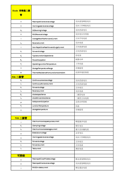
Diode肖特基二极管
V
Peakrepetitivereversevoltage
反向重复峰值电压
V
Workingpeakreversevoltage
反向工作峰值电压
VR
DCBlockingVoltage
反向直流电压
V
RMSReverseVoltage
反向电压有效值
I
AverageRectifiedForwardCurrent
反向传输电容
Rg
Gateresistance
栅极电阻
t
Turn-ondelaytime
开通延迟时间
tr
Risetime
上升时间
t
Turn-offdelaytime
ADA-4643 Datasheet说明书

ADA-4643Silicon Bipolar Darlington Amplifi erData SheetAttention: Observe precautions forhandling electrostatic sensitive devices.ESD Machine Model (Class A)ESD Human Body Mode (Class 1B)Refer to Avago Application Note A004R:Electrostatic Discharge, Damage and Control.RFinGNDRFout & VdGND DescriptionAvago Technologies’ ADA-4643 is an economical, easy-to-use, general purpose silicon bipolar RFIC gain block am-plifi ers housed in a 4-lead SC-70 (SOT-343) surface mount plastic package which requires only half the board space of a SOT-143 package.The Darlington feedback structure provides inherent broad bandwidth performance, resulting in useful ope-rating frequency up to 2.5 GHz. This is an ideal device forsmall-signal gain cascades or IF amplifi cation. ADA-4643 is fabricated using Avago’s HP25 silicon bipolarprocess, which employs a double-diff used single poly-silicon process with self-aligned submicron emitter geometry. The process is capable of simultaneous high f T and high NPN breakdown (25 GHz f T at 6 V BVCEO). The process utilizes industry standard device oxide isolation technologies and submicron aluminum multilayer inter-connect to achieve superior performance, high uniformity, and proven reliability.Surface Mount PackageSOT-343Pin Connections and Package MarkingNote:Top View. Package marking provides orientation and identifi cation.“2T” = Device Code“x” = Date code character identifi es month of manufacture.V CC = 5 VRF inputRF Features∙ Small Signal gain amplifi er∙ Operating frequency DC – 2.5 GHz ∙ Unconditionally stable ∙ 50 Ohms input & output∙ Flat, Broadband Frequency Response up to 1 GHz∙ Operating Current: 20 to 60 mA ∙ Industry standard SOT-343 package∙ Lead-free option available Specifi cations900 MHz, 3.5 V, 35 mA (typ.)∙ 17 dB associated gain ∙ 13.4 dBm P 1dB ∙ 28.3 dBm OIP 3∙ 4 dB noise fi gure∙ VSWR < 2.2 throughput operating frequency ∙ Single supply, typical I d = 35 mAApplications∙ Cellular/PCS/WLL base stations ∙ Wireless data/WLAN ∙ Fiber-optic systems ∙ ISMTypical Biasing Confi gurationADA-4643 Electrical Specifi cationsT A = 25° C, Zo = 50 Ω, Pin = -25 dBm, I d = 35 mA (unless specifi ed otherwise)SymbolParameter and Test Condition:I d = 35 mA, Zo = 50 ΩFrequencyUnitsMin.Typ.Max.Std. Dev.V d Device Voltage I d = 35 mA V 3.2 3.5 3.9Gp Power Gain (|S 21|)2100 MHz 900 MHz [1,2]dB15.517.517.018.5∆Gp Gain Flatness 100 to 900 MHz 0.1 to 2 GHz dB 0.51.8F 3dB 3 dB BandwidthGHz3.2VSWR in Input Voltage Standing Wave Ratio0.1 to 6 GHz2.0:1VSWR out Output Voltage Standing Wave Ratio 0.1 to 6 GHz 1.6:1NF 50 Ω Noise Figure100 MHz 900 MHz [1,2]dB 3.94.00.070.1P 1dB Output Power at 1dB Gain Compression 100 MHz 900 MHz [1,2]dBm 14.713.4OIP 3Output 3rd Order Intercept Point100 MHz [3]900 MHz [1,2]dBm 29.028.3DV/dTDevice Voltage Temperature Coeffi cientmV/°C-5.3Notes:1. Typical value determined from a sample size of 500 parts from 3 wafers.2. Measurement obtained using production test board described in the block diagram below.3. I) 900 MHz OIP 3 test condition: F1 = 900 MHz, F2 = 905 MHz and Pin = -25 dBm per tone. II) 100 MHz OIP 3 test condition: F1 = 100 MHz, F2 = 105 MHz and Pin = -25 dBm per tone.ADA-4643 Absolute Maximum Ratings [1]SymbolParameterUnitsAbsolute MaximumI d Device CurrentmA 70P diss Total Power Dissipation [2]mW 270P in max.RF Input Power dBm 18T j Channel Temperature ︒C 150T STG Storage Temperature ︒C -65 to 150θjcThermal Resistance [3]︒C/W152Notes:1. Operation of this device above any one of these parameters may cause permanent damage.2. Ground lead temperature is 25° C. Derate 6.6 mW/°C for TL >109° C.3. Junction-to-case thermal resistance measured using 150° C Liquid Crystal Measurement method.Block diagram of 900 MHz production test board used for V d , Gain, P 1dB , OIP 3, and NF measurements.Circuit losses have been de-embedded from actual measurements.Product Consistency Distribution Charts at 900 MHz, I d= 35 mAGAIN (dB)300250200150100500V d (V)300250200150100500*********************************=15.5,Nominal=17,USL=18.5Figure 2. V d *********************=3.2,Nominal=3.5,USL=3.9Notes:1. Statistics distribution determined from a sample size of 500 parts taken from 3 diff erent wafers.2. Future wafers allocated to this product may have typical values anywhere between the minimum and maximum specifi cation limits.ADA-4643 Typical Performance Curves (at 25° C, unless specifi ed otherwise)Figure 3. Gain vs. Frequency at I d = 35 mA.Figure 4. P 1dB vs. Frequency at I d = 35 mA.Figure 5. OIP 3 vs. Frequency at I d = 35 mA.Figure 6. NF vs. Frequency at I d = 35 mA.Figure 7. Id vs. V d and Temperature.Figure 8. Gain vs. I d and Temperature at 900 MHz.FREQUENCY (GHz)G A I N (d B )62135420151050FREQUENCY (GHz)P 1d B (d B m )06213542015105FREQUENCY (GHz)O I P 3 (d B m )062135430252015105FREQUENCY (GHz)0621354N F (d B )65432V d (V)I d (m A )706050403020100I d (mA)G A I N (d B )18171615141312Figure 9. P 1dB vs. I d and Temperature at 900 MHz.Figure 10. OIP 3 vs. I d and Temperature at 900 MHz.Figure 11. NF vs. I d and Temperature at 900 MHz.Figure 12. Gain vs. I d and Frequency (GHz).Figure 13. P 1dB vs. I d and Frequency (GHz).Figure 14. OIP 3 vs. I d and Frequency (GHz).I d (mA)O I P 3 (d B m )0.10.50.91.52.02.53456403530252015105I d (mA)P 1d B (d B m )20151050-5-10I d (mA)O I P 3 (d B m )I d (mA)N F (d B )16543210I d (mA)G A I N (d B )402010303030302018161412108I d (mA)P 1d B (d B m )2520151050-5-10Figure 15. NF vs. I d and Frequency (GHz).Figure 16. Input Return Loss vs. I d and Frequency (GHz).Figure 17. Output Return Loss vs. I d and Frequency (GHz).I d (mA)N F (d B )65.554.543.53FREQUENCY (GHz)I R L(d B )-5-10-15-20FREQUENCY (GHz)O R L (d B )0-5-10-15-20-25Freq. GHz11 211222K Mag. Ang. dB Mag. Ang. Mag. Ang. Mag. Ang.0.10.172 1.1 17.2 7.246 175.9 0.093 -0.8 0.245 -4.1 1.10.5 0.202 10 17.04 7.113 160.2 0.091 -4.5 0.245 -12.6 1.10.9 0.277 12.3 16.67 6.814 144.7 0.088 -7.4 0.269 -20.4 1.11.0 0.286 9.9 16.56 6.726 141.1 0.087 -7.9 0.274 -23.1 1.11.5 0.349 -2.8 15.98 6.292 124.2 0.083 -9.3 0.28 -37.6 1.11.9 0.375 -11.3 15.54 5.984 111.4 0.080 -9.5 0.273 -48.9 1.22.0 0.382 -13.8 15.44 5.918 108.3 0.080 -9.5 0.271 -51.7 1.22.5 0.397 -24.2 14.93 5.581 93.20.078-8.9 0.249 -65.8 1.23.0 0.402 -34.7 14.475.29 78.60.078 -7.8 0.22 -81.7 1.33.5 0.394 -46 14.025.021 64.2 0.079 -6.6 0.192 -100.9 1.34.0 0.378 -58.7 13.58 4.775 50 0.082 -5.4 0.176 -123.8 1.34.5 0.361 -73.1 13.16 4.55 35.9 0.087 -4.6 0.179 -148.6 1.35.0 0.340 -89.3 12.64 4.284 21.9 0.094 -4.9 0.191 -169.9 1.35.5 0.328 -107.1 12.15 4.05 8.3 0.102 -5.9 0.212 173.3 1.26.0 0.318 -124.8 11.6 3.803 -5.4 0.112 -8.3 0.233 158.2 1.26.5 0.299 -141.1 11.09 3.584 -18.6 0.124 -11.5 0.25 141.6 1.17.0 0.274 -159.7 10.56 3.371 -32 0.138 -16.5 0.27 123 1.17.5 0.243 177.3 9.96 3.149 -45.6 0.150 -22.8 0.3 103.6 1.18.0 0.222 148.7 9.29 2.914 -59.1 0.161 -30 0.337 84.8 1.18.5 0.226 119.9 8.41 2.632 -71.8 0.168 -36.7 0.381 70.1 1.19.0 0.26 95.4 7.62 2.406 -83.7 0.177 -43 0.429 58.4 1.19.5 0.305 75.2 6.67 2.155-96.1 0.187 -49.9 0.48148.4 1.110.0 0.356 60.1 5.82 1.954 -107.1 0.195-57.3 0.529 39.7 1Notes:1. S-parameters are measured on a microstrip line made on 0.025 inch thick alumina carrier. The input reference plane is at the end of the input lead.The output reference plane is at the end of the output lead.Freq. GHz11211222K Mag. Ang. dB Mag. Ang. Mag. Ang. Mag. Ang.0.1 0.151 1.6 17.51 7.504 175.9 0.091 -0.8 0.223 -4.1 1.10.5 0.185 13.1 17.35 7.367 160.1 0.09 -4.2 0.224 -11.7 1.10.9 0.265 14.9 16.98 7.06 144.6 0.087 -7 0.251 -19 1.11.0 0.272 12.4 16.86 6.97 140.9 0.086 -7.5 0.256 -21.7 1.11.50.340 -0.7 16.27 6.511 123.9 0.082 -8.8 0.264 -36.2 1.11.9 0.367 -9.5 15.82 6.178 111 0.080 -9.1 0.259 -47.6 1.22.0 0.373 -12.1 15.72 6.107 108 0.079 -9.1 0.256-50.3 1.22.5 0.39 -22.7 15.19 5.745 92.8 0.078 -8.5 0.236 -64.4 1.23.0 0.395 -33 14.715.436 78.3 0.077 -7.3 0.209 -80.4 1.33.5 0.387 -44.3 14.235.149 63.9 0.079 -6 0.181 -99.9 1.34.0 0.370 -57.4 13.79 4.89 49.9 0.082 -4.8 0.166 -123.4 1.34.5 0.353 -71.6 13.36 4.657 35.9 0.087-3.9 0.17 -148.9 1.35.0 0.332 -87.7 12.84 4.383 21.9 0.093 -4.2 0.185 -170.6 1.25.5 0.319 -106 12.34 4.141 8.3 0.102 -5.1 0.207 172.5 1.26.0 0.310 -123.6 11.8 3.889 -5.4 0.112 -7.5 0.23 157.5 1.26.5 0.293 -140.2 11.28 3.666 -18.6 0.124 -10.8 0.248 140.9 1.17.0 0.266 -158.8 10.75 3.449 -32 0.138 -15.8 0.27 122.3 1.17.5 0.238 177.8 10.15 3.219 -45.5 0.151 -22.2 0.301 103 1.18.0 0.217 148.5 9.48 2.979 -59 0.161 -29.3 0.34 84.3 1.18.5 0.222 119.5 8.62 2.697 -71.7 0.169 -36.1 0.385 69.6 1.19.0 0.256 95 7.81 2.458 -83.4 0.178 -42.5 0.434 57.9 1.19.5 0.300 74.9 6.88 2.208 -95.8 0.188 -49.5 0.486 47.9 110.0 0.357 59.1 6.01 1.996 -107.2 0.196 -56.9 0.53439.2 1Notes:1. S-parameters are measured on a microstrip line made on 0.025 inch thick alumina carrier. The input reference plane is at the end of the input lead.The output reference plane is at the end of the output lead.Freq. GHz11211222K Mag. Ang. dB Mag. Ang. Mag. Ang. Mag. Ang.0.1 0.137 2.417.72 7.691 175.9 0.09-0.70.207 -4 1.10.5 0.174 15.317.567.547 1600.089 -4 0.209-10.9 1.10.9 0.25717.417.19 7.234 144.5 0.086 -6.8 0.238-17.6 1.11.0 0.267 14.717.087.144140.80.085 -7.2 0.243 -20.3 1.11.50.334 0.716.47 6.664 123.70.081 -8.50.253-34.8 1.11.9 0.36 -8.416.01 6.317 110.70.079 -8.7 0.249 -46.1 1.12.0 0.367-10.915.91 6.241107.70.079 -8.7 0.247-48.9 1.22.5 0.386-21.615.36 5.86292.5 0.077 -8.1 0.227 -62.9 1.23.0 0.39 -32.114.865.534 78 0.077 -7 0.201 -78.9 1.23.5 0.382-43.414.385.237 63.6 0.078 -5.70.174 -98.4 1.34.0 0.365 -56.4 13.93 4.97149.7 0.081 -4.5 0.159-122.3 1.34.5 0.348 -70.813.5 4.732 35.7 0.086-3.6 0.164-148.3 1.35.0 0.327 -86.8 12.97 4.45 21.7 0.093 -3.9 0.179-170.4 1.25.5 0.314 -105.112.48 4.205 8.20.101-4.8 0.202172.6 1.26.0 0.304-122.811.93 3.947 -5.5 0.112 -7.1 0.226 157.6 1.26.5 0.287 -139.6 11.41 3.721 -18.70.124 -10.40.245 140.9 1.17.0 0.26-159.1 10.88 3.498 -32 0.138 -15.40.268122.3 1.17.5 0.232177.610.28 3.264 -45.6 0.151 -21.80.3 102.9 1.18.0 0.213147.8 9.6 3.02 -59.10.161 -28.90.339 84.2 1.18.5 0.218120.28.7 2.724 -71.7 0.169 -35.80.385 69.5 1.19.0 0.2694.27.95 2.498 -83.70.179-42.10.434 57.9 1.19.5 0.30374 6.98 2.233 -96.20.189-49.20.48747.9 110.0 0.35259.4 6.14 2.027-107.1 0.196 -56.60.53539.1 1Notes:1. S-parameters are measured on a microstrip line made on 0.025 inch thick alumina carrier. The input reference plane is at the end of the input lead.The output reference plane is at the end of the output lead.Freq. GHz11211222K Mag. Ang. dB Mag. Ang. Mag. Ang. Mag. Ang.0.1 0.126 2.4 17.88 7.834 175.9 0.089 -0.7 0.194 -3.8 1.10.5 0.165 18.1 17.73 7.696 159.9 0.088 -3.8 0.196 -9.9 1.10.9 0.252 19.6 17.36 7.377 144.3 0.085 -6.4 0.227 -16.1 1.11.0 0.261 16.4 17.24 7.28 140.6 0.085 -6.9 0.233 -18.8 1.11.5 0.33 2 16.63 6.787 123.3 0.081 -8.2 0.244 -33.2 1.11.9 0.359 -7.4 16.16 6.424 110.3 0.079 -8.4 0.241 -44.4 1.12.0 0.365 -9.8 16.05 6.343 107.2 0.078 -8.4 0.239 -47.2 1.12.5 0.386 -21 15.49 5.948 91.9 0.077 -7.8 0.221 -61 1.23.0 0.387 -31.5 14.985.61 77.4 0.077 -6.7 0.195 -76.8 1.23.5 0.381 -43 14.495.301 63.1 0.078 -5.5 0.168 -96.2 1.34.0 0.363 -56 14.025.025 49 0.081 -4.3 0.153 -120.3 1.34.5 0.344 -70.7 13.58 4.777 35 0.086 -3.5 0.157 -146.9 1.35.0 0.323 -87.3 13.04 4.488 21 0.093 -3.7 0.172 -169.4 1.25.5 0.31 -105.8 12.54 4.235 7.5 0.101 -4.6 0.195 173.4 1.26.0 0.301 -123.6 11.98 3.971 -6.2 0.111 -6.9 0.22 158.2 1.26.5 0.281 -140.6 11.44 3.735 -19.4 0.124 -10.2 0.239 141.4 1.17.0 0.257 -159.9 10.9 3.507 -32.7 0.138 -15.2 0.262 122.5 1.17.5 0.228 176.3 10.29 3.271 -46.3 0.151 -21.5 0.294 103 1.18.0 0.212 145.6 9.61 3.022 -59.8 0.161 -28.6 0.333 84.3 1.18.5 0.218 117.8 8.72 2.728 -72.4 0.169 -35.6 0.38 69.5 1.19.0 0.257 92.7 7.94 2.494 -84.1 0.178 -41.8 0.429 57.9 1.19.5 0.302 72.9 6.98 2.234 -96.4 0.189 -48.9 0.482 47.9 110.0 0.359 57.7 6.11 2.02 -107.7 0.196 -56.4 0.531 39.2 1Notes:1. S-parameters are measured on a microstrip line made on 0.025 inch thick alumina carrier. The input reference plane is at the end of the input lead.The output reference plane is at the end of the output lead.11Ordering InformationPart NumberNo. of DevicesContainerADA-4643-TR1 3000 7” ReelADA-4643-TR2 10000 13” ReelADA-4643-BLK 100 antistatic bag ADA-4643-TR1G 3000 7” ReelADA-4643-TR2G 10000 13” Reel ADA-4643-BLKG 100antistatic bagNote: For lead-free option, the part number will have the character “G” at the end.Package DimensionsOutline 43SOT-343 (SC70 4-lead)Recommended PCB Pad Layout for Avago’s SC70 4L/SOT-343 ProductsDIMENSIONS (mm)MIN.1.151.851.800.800.800.000.150.550.100.10MAX.1.352.252.401.101.000.100.400.700.200.46SYMBOL E D HE A A2A1b b1c LNOTES:1. All dimensions are in mm.2. Dimensions are inclusive of plating.3. Dimensions are exclusive of mold flash & metal burr.4. All specifications comply to EIAJ SC70.5. Die is facing up for mold and facing down for trim/form, ie: reverse trim/form.6. Package surface to be mirror finish.1.30(0.051)Dimensions inmm (inches)(0.039)For product information and a complete list of distributors, please go to our web site: Avago, Avago Technologies, and the A logo are trademarks of Avago Technologies in the United States and other countries.Data subject to change. Copyright © 2005-2012 Avago Technologies. All rights reserved. Obsoletes 5989-3753EN AV02-3598EN - June 8, 2012(COVER TAPE THICKNESS)DESCRIPTIONSYMBOL SIZE (mm)SIZE (INCHES)LENGTH WIDTH DEPTH PITCHBOTTOM HOLE DIAMETERA 0B 0K 0P D 12.40 ± 0.102.40 ± 0.101.20 ± 0.104.00 ± 0.101.00 + 0.250.094 ± 0.0040.094 ± 0.0040.047 ± 0.0040.157 ± 0.0040.039 + 0.010CAVITYDIAMETER PITCH POSITIOND P 0E 1.50 ± 0.104.00 ± 0.101.75 ± 0.100.061 + 0.0020.157 ± 0.0040.069 ± 0.004PERFORATIONWIDTHTHICKNESS W t 18.00 + 0.30 - 0.100.254 ± 0.020.315 + 0.0120.0100 ± 0.0008CARRIER TAPE CAVITY TO PERFORATION (WIDTH DIRECTION)CAVITY TO PERFORATION (LENGTH DIRECTION)FP 23.50 ± 0.052.00 ± 0.050.138 ± 0.0020.079 ± 0.002DISTANCEWIDTHTAPE THICKNESSC T t 5.40 ± 0.100.062 ± 0.0010.205 + 0.0040.0025 ± 0.0004COVER TAPE Device OrientationTape DimensionsFor Outline 4TUSER FEEDEND VIEWTOP VIEW。
TD62783AFG中文资料
TD62783,784APG/AFG
TOSHIBA Bipolar Digital Integrated Circuit Silicon Monolithic
TD62783APG,TD62783AFG,TD62784APG,TD62784AFG
8 ch High-Voltage Source Driver
V mA/ch
V
V mA W
°C °C
Note 1: Only TD62783APG/AFG Note 2: Only TD62784APG/AFG Note 3: Derated above 25°C in the proportion of 11.7 W/°C (APG type), 7.7 W/°C (AFG type)
TD62784APG/AFG
TD62783APG/AFG TD62784APG/AFG Input voltage TD62783APG/AFG TD62784APG/AFG Supply current Clamp diode reverse current Clamp diode forward voltage Turn-ON delay
2
2006-06-14
元器件交易网
TD62783,784APG/AFG
Recommended Operating Conditions (Ta = −40 to 80°C)
Characteristics
Symbol
Test Condition
Min Typ. Max Unit
Input voltage VIN (V)
Output current IOUT (mA)
TD62783,784APG/AFG
数字电感电容表
图2
Visage eXPert PDF Copyright ?1998,2005 Visage Software This document was created with free TRIAL version of Visage eXPert PDF.This watermark will be removed after purchasing the licensed full version of Visage eXPert PDF. Please visit /products/expertpdf/ for more details
该系列仪表是一台精密仪器,使用者不要随意更改电路。
1.请注意防水、防尘 、防摔 ;
2.不宜在高温高湿、易燃易爆和强磁场的环境下存放、使用仪表;
3 . 请 使 用 湿 布 和 温 和 的 清 洁 剂 清 洁 仪 表 外 表 ,不 要 使 用 研 磨 剂 及 酒 精 等 烈
性溶剂;
4.如果长时间不使用,应取出电池,防止电池漏液腐蚀仪表;
量程
准确度
分辨力 测试频度 通过电流
2mH
1uH
1kHz
150uA
20mH ?(2 .0 %+5) 10uH
1kHz
150uA
200mH
100uH
1kHz
150uA
2H
?(5 .0 %+5) 1mH
1kHz
150uA
DF6113说明书

DIM
Ext. Current Control
FB
Load Current Measurement
OVP Comp.
LOGIC CONTROL
1.0V Driver
CS OVP GATE
Hi-Freq. Oscillator
GND
(DF6113)
PIN
名称
1
VCC
2
OVP
3
CMP
4
DIM
5
FB
6
CS
ENA 为高或悬空时,芯片工作;ENA=GND,芯片截止
ENA+DIM(低电压最亮)调光
ENA (>3.0V)
DIM
R DIM R FB
R OUT
PIN(DIM) PIN(FB) LED-
ENA 电压>3.0V;最亮时的灯电流近似于前文(灯电流调节)中 100%亮度
输出短路保护 利用 FB 管脚外部串联的 RFB = 2k 防止芯片被短路瞬间的高压击穿。当输出短路时,芯片自 带的保护使 MOS 停止工作,以防止 MOS 和芯片烧毁。
C5
C6
226
475
50V
50V
C1206
R3 1K R0603
ENA DIM
R4
4.7K R0603
R DIM
12K R0603
C4
104 C0603
1
VCC
2
OVP
3
CMP
4
DIM
DF6113
8
GATE
7
GND
6
CS
5
FB
RFB
2K R0603
Rout 3R