HIP4081
HIP4082IP中文数据手册

-
µA
6.8 7.6 8.25 6.5 8.5
V
6.5 7.1 7.8 6.25 8.1
V
0.17 0.4 0.75 0.15 0.90
V
AHB, BHB Undervoltage Threshold INPUT PINS: ALI, BLI, AHI, BHI, & DIS
VHBUV
Referenced to AHS & BHS
VDD Falling Undervoltage Threshold
欠压滞后
IDD
IDDO
IAHBL , BHBL
I
IAHBH , BHBH
I
IAHBO , BHBO
I
I
HLK
V DDUV+ V DDUVUVHYS
All inputs = 0V, R DEL = 100K
All inputs = 0V, R
2注0:V/所ns有的电压都是相对V
SS 除非另有规定.
热阻
SOIC封装. . . . . . . . . . . . . . . . . . . . . . . . . .D.IP. .封装. . . . . . . . . . . . . . . . . . . . . . . . . 最大. .功. .率. 耗散. . . . . . . . . . . . . . . . . . . . . . . .见 曲存线储温度范围. . . . . . . . . . . . . . . . . .-65°C至 +操1作50最°C大.结温. . . . . . . . . . . . . . . . . . +焊1接50温°C度(10秒). . . . . . . . . . . . . . . . . . . . +3(00对°C于SOIC - 铅针头))
GigaSPEED XL 3071E-B ETL Verified Category 6 U UTP
GigaSPEED XL® 3071E-B ETL Verified Category 6 U/UTP Cable, lowsmoke zero halogen, white jacket, 4 pair count, 1000 ft (305 m) length,reelProduct ClassificationRegional Availability EMEAPortfolio SYSTIMAX®Product Type Twisted pair cableProduct Brand GigaSPEED XL®General SpecificationsProduct Number3071EANSI/TIA Category6Cable Component Type HorizontalCable Type U/UTP (unshielded)Conductor Type, singles SolidConductors, quantity8Jacket Color WhitePairs, quantity4Separator Type BisectorTransmission Standards ANSI/TIA-568.2-D | CENELEC EN 50288-6-1 | ISO/IEC 11801 Class E DimensionsCable Length304.8 m | 1000 ftDiameter Over Insulated Conductor 1.041 mm | 0.041 inDiameter Over Jacket, nominal 5.918 mm | 0.233 inJacket Thickness0.559 mm | 0.022 inConductor Gauge, singles23 AWG13Page ofCross Section DrawingElectrical Specificationsdc Resistance Unbalance, maximum 5 %dc Resistance, maximum7.61 ohms/100 m | 2.32 ohms/100 ftDielectric Strength, minimum2500 VdcMutual Capacitance at Frequency 5.6 nF/100 m @ 1 kHzNominal Velocity of Propagation (NVP)70 %Operating Frequency, maximum300 MHzOperating Voltage, maximum80 VRemote Powering Fully complies with the recommendations set forth by IEEE 802.3bt (Type4) for the safe delivery of power over LAN cable when installed accordingto ISO/IEC 14763-2, CENELEC EN 50174-1, CENELEC EN 50174-2 or TIATSB-184-ASegregation Class cMaterial SpecificationsConductor Material Bare copperInsulation Material PolyolefinJacket Material Low Smoke Zero Halogen (LSZH)Separator Material PolyolefinPage of23Mechanical SpecificationsPulling Tension, maximum11.34 kg | 25 lbEnvironmental SpecificationsInstallation temperature0 °C to +60 °C (+32 °F to +140 °F)Operating Temperature-20 °C to +60 °C (-4 °F to +140 °F)Acid Gas Test Method EN 50267-2-3EN50575 CPR Cable EuroClass Fire Performance B2caEN50575 CPR Cable EuroClass Smoke Rating s1aEN50575 CPR Cable EuroClass Droplets Rating d0EN50575 CPR Cable EuroClass Acidity Rating a1Environmental Space Low Smoke Zero Halogen (LSZH)Smoke Test Method IEC 61034-2Packaging and WeightsCable weight38.097 kg/km | 25.6 lb/kftPackaging Type ReelRegulatory Compliance/CertificationsAgency ClassificationCENELEC EN 50575 compliant, Declaration of Performance (DoP) availableCHINA-ROHS Below maximum concentration valueISO 9001:2015Designed, manufactured and/or distributed under this quality management system REACH-SVHC Compliant as per SVHC revision on /ProductCompliance ROHSCompliantPage of33。
MAX4081SASA中文资料
Continuous Power Dissipation (TA = +70°C) 8-Pin µMAX (derate 4.5mW/°C above +70°C) .............362mW 8-Pin SO (derate 5.88mW/°C above +70°C)................471mW
Stresses beyond those listed under “Absolute Maximum Ratings” may cause permanent damage to the device. These are stress ratings only, and functional operation of the device at these or any other conditions beyond those indicated in the operational sections of the specifications is not implied. Exposure to absolute maximum rating conditions for extended periods may affect device reliability.
HIP4081AIB中文资料
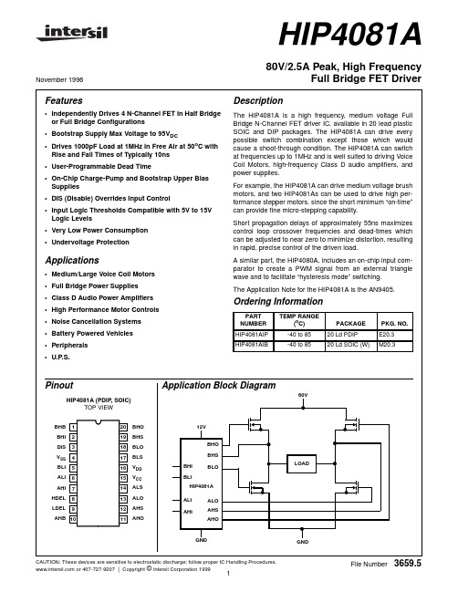
HIP4081A
November 1996
80V/2.5A Peak, High Frequency Full Bridge FET Driver
Features
• Independently Drives 4 N-Channel FET in Half Bridge or Full Bridge Configurations
元器件交易网
HIP4081A
Absolute Maximum Ratings
Thermal Information
Supply Voltage, VDD and VCC. . . . . . . . . . . . . . . . . . . . -0.3V to 16V Logic I/O Voltages . . . . . . . . . . . . . . . . . . . . . . . -0.3V to VDD +0.3V Voltage on AHS, BHS . . . . -6.0V (Transient) to 80V (25oC to 125oC) Voltage on AHS, BHS . . . -6.0V (Transient) to 70V (-55oC to 125oC)
Supplies • DIS (Disable) Overrides Input Control • Input Logic Thresholds Compatible with 5V to 15V
Logic Levels • Very Low Power Consumption • Undervoltage Protection
Description
The HIP4081A is a high frequency, medium voltage Full Bridge N-Channel FET driver IC, available in 20 lead plastic SOIC and DIP packages. The HIP4081A can drive every possible switch combination except those which would cause a shoot-through condition. The HIP4081A can switch at frequencies up to 1MHz and is well suited to driving Voice Coil Motors, high-frequency Class D audio amplifiers, and power supplies.
Motorola 3.5 kHz 产品说明书
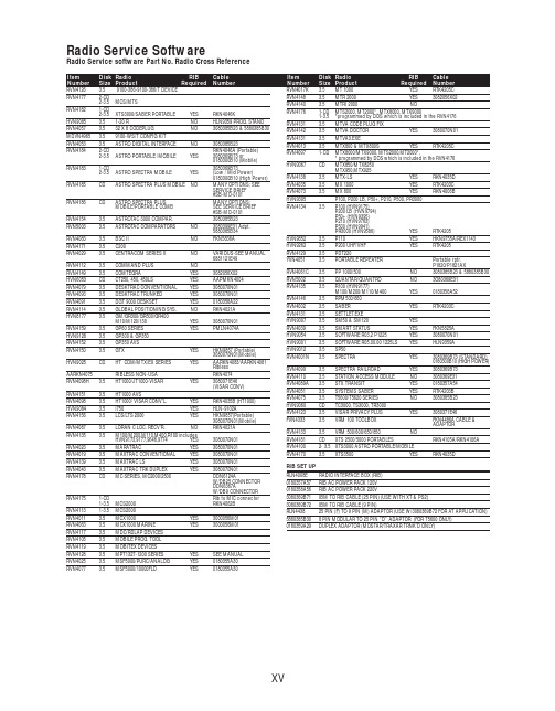
RVN4126 3.59100-386-9100-386/T DEVICERVN41772-CD2-3.5MCS/MTSRVN41821-CD2-3.5XTS3000/SABER PORTABLE YES RKN4046KHVN9085 3.51-20 R NO HLN9359 PROG. STAND RVN4057 3.532 X 8 CODEPLUG NO3080385B23 & 5880385B30 MDVN4965 3.59100-WS/T CONFIG KITRVN4053 3.5ASTRO DIGITAL INTERFACE NO3080385B23RVN41842-CD RKN4046A (Portable) 2-3.5ASTRO PORTABLE /MOBILE YES3080369B73 or0180300B10 (Mobile) RVN41831-CD3080369B732-3.5ASTRO SPECTRA MOBILE YES(Low / Mid Power)0180300B10 (High Power) RVN4185CD ASTRO SPECTRA PLUS MOBILE NO MANY OPTIONS; SEESERVICE BRIEF#SB-MO-0101RVN4186CD ASTRO SPECTRA PLUS MANY OPTIONS;MOBILE/PORTABLE COMB SEE SERVICE BRIEF#SB-MO-0101RVN4154 3.5ASTROTAC 3000 COMPAR.3080385B23RVN5003 3.5ASTROTAC COMPARATORS NO3080399E31 Adpt.5880385B34RVN4083 3.5BSC II NO FKN5836ARVN4171 3.5C200RVN4029 3.5CENTRACOM SERIES II NO VARIOUS-SEE MANUAL6881121E49RVN4112 3.5COMMAND PLUS NORVN4149 3.5COMTEGRA YES3082056X02HVN6053CD CT250, 450, 450LS YES AAPMKN4004RVN4079 3.5DESKTRAC CONVENTIONAL YES3080070N01RVN4093 3.5DESKTRAC TRUNKED YES3080070N01RVN4091 3.5DGT 9000 DESKSET YES0180358A22RVN4114 3.5GLOBAL POSITIONING SYS.NO RKN4021AHVN8177 3.5GM/GR300/GR500/GR400M10/M120/130YES3080070N01RVN4159 3.5GP60 SERIES YES PMLN4074AHVN9128 3.5GP300 & GP350RVN4152 3.5GP350 AVSRVN4150 3.5GTX YES HKN9857 (Portable)3080070N01(Mobile) HVN9025CD HT CDM/MTX/EX SERIES YES AARKN4083/AARKN4081RiblessAARKN4075RIBLESS NON-USA RKN4074RVN4098H 3.5HT1000/JT1000-VISAR YES3080371E46(VISAR CONV)RVN4151 3.5HT1000 AVSRVN4098 3.5HT1000/ VISAR CONV’L.YES RKN4035B (HT1000) HVN9084 3.5i750YES HLN-9102ARVN4156 3.5LCS/LTS 2000YES HKN9857(Portable)3080070N01(Mobile) RVN4087 3.5LORAN C LOC. RECV’R.NO RKN4021ARVN4135 3.5M100/M200,M110,M400,R100 includesHVN9173,9177,9646,9774YES3080070N01RVN4023 3.5MARATRAC YES3080070N01RVN4019 3.5MAXTRAC CONVENTIONAL YES3080070N01RVN4139 3.5MAXTRAC LS YES3080070N01RVN4043 3.5MAXTRAC TRK DUPLEX YES3080070N01RVN4178CD MC SERIES, MC2000/2500DDN6124AW/DB25 CONNECTORDDN6367AW/DB9 CONNECTOR RVN41751-CD Rib to MIC connector 1-3.5MCS2000 RKN4062BRVN41131-3.5MCS2000RVN4011 3.5MCX1000YES3000056M01RVN4063 3.5MCX1000 MARINE YES3000056M01RVN4117 3.5MDC/RDLAP DEVICESRVN4105 3.5MOBILE PROG. TOOLRVN4119 3.5MOBITEX DEVICESRVN4128 3.5MPT1327-1200 SERIES YES SEE MANUALRVN4025 3.5MSF5000/PURC/ANALOG YES0180355A30RVN4077 3.5MSF5000/10000FLD YES0180355A30RVN4017K 3.5MT 1000YES RTK4205CRVN4148 3.5MTR 2000YES3082056X02RVN4140 3.5MTRI 2000NORVN41761-CD MTS2000, MT2000*, MTX8000, MTX90001-3.5*programmed by DOS which is included in the RVN4176RVN4131 3.5MTVA CODE PLUG FIXRVN4142 3.5MTVA DOCTOR YES3080070N01RVN4131 3.5MTVA3.EXERVN4013 3.5MTX800 & MTX800S YES RTK4205CRVN4097 1-CD MTX8000/MTX9000,MTS2000,MT2000*,* programmed by DOS which is included in the RVN4176HVN9067CD MTX850/MTX8250MTX950,MTX925RVN4138 3.5MTX-LS YES RKN4035DRVN4035 3.5MX 1000YES RTK4203CRVN4073 3.5MX 800YES RKN4006BHVN9395 P100, P200 LB, P50+, P210, P500, PR3000RVN4134 3.5P100 (HVN9175)P200 LB (HVN9794)P50+ (HVN9395)P210 (HVN9763)P500 (HVN9941)PR3000 (HVN9586)YES RTK4205HVN9852 3.5P110YES HKN9755A/REX1143 HVN9262 3.5P200 UHF/VHF YES RTK4205RVN4129 3.5PDT220YVN4051 3.5PORTABLE REPEATER Portable rptr.P1820/P1821AXRVN4061C 3.5PP 1000/500NO3080385B23 & 5880385B30 RVN5002 3.5QUANTAR/QUANTRO NO3O80369E31RVN4135 3.5R100 (HVN9177)M100/M200/M110/M400YES0180358A52RVN4146 3.5RPM500/660RVN4002 3.5SABER YES RTK4203CRVN4131 3.5SETTLET.EXEHVN9007 3.5SM50 & SM120YESRVN4039 3.5SMART STATUS YES FKN5825AHVN9054 3.5SOFTWARE R03.2 P1225YES3080070N01HVN9001 3.5SOFTWARE R05.00.00 1225LS YES HLN9359AHVN9012 3.5SP50RVN4001N 3.5SPECTRA YES3080369B73 (STANDARD)0180300B10 (HIGH POWER) RVN4099 3.5SPECTRA RAILROAD YES3080369B73RVN4110 3.5STATION ACCESS MODULE NO3080369E31RVN4089A 3.5STX TRANSIT YES0180357A54RVN4051 3.5SYSTEMS SABER YES RTK4203BRVN4075 3.5T5600/T5620 SERIES NO3080385B23HVN9060CD TC3000, TS3000, TR3000RVN4123 3.5VISAR PRIVACY PLUS YES3080371E46FVN4333 3.5VRM 100 TOOLBOX FKN4486A CABLE &ADAPTORRVN4133 3.5VRM 500/600/650/850NORVN4181CD XTS 2500/5000 PORTABLES RKN4105A/RKN4106A RVN41002- 3.5XTS3000 ASTRO PORTABLE/MOBILERVN4170 3.5XTS3500YES RKN4035DRIB SET UPRLN4008E RADIO INTERFACE BOX (RIB)0180357A57RIB AC POWER PACK 120V0180358A56RIB AC POWER PACK 220V3080369B71IBM TO RIB CABLE (25 PIN) (USE WITH XT & PS2)3080369B72IBM TO RIB CABLE (9 PIN)RLN443825 PIN (F) TO 9 PIN (M) ADAPTOR (USE W/3080369B72 FOR AT APPLICATION) 5880385B308 PIN MODULAR TO 25 PIN ”D” ADAPTOR (FOR T5600 ONLY)0180359A29DUPLEX ADAPTOR (MOSTAR/TRAXAR TRNK’D ONLY)Item Disk Radio RIB Cable Number Size Product Required Number Item Disk Radio RIB Cable Number Size Product Required NumberUtilizing your personal computer, Radio Service Software (RSS)/Customer Programming Software (CPS)/CustomerConfiguration Software (CCS) enables you to add or reprogram features/parameters as your requirements change. RSS/CPS/CCS is compatible with IBM XT, AT, PS/2 models 30, 50, 60 and 80.Requires 640K RAM. DOS 3.1 or later. Consult the RSS users guide for the computer configuration and DOS requirements. (ForHT1000, MT/MTS2000, MTX838/8000/9000, Visar and some newer products —IBM model 386, 4 MEG RAM and DOS 5.0 or higher are recommended.) A Radio Interface Box (RIB) may be required as well as the appropriate cables. The RIB and cables must be ordered separately.Licensing:A license is required before a software (RVN) order is placed. The software license is site specific (customer number and ultimate destination tag). All sites/locations must purchase their own software.Be sure to place subsequent orders using the original customer number and ship-to-tag or other licensed sites; ordering software without a licensed customer number and ultimate tag may result in unnecessary delays. To obtain a no charge license agreement kit, order RPX4719. To place an order in the U.S. call 1-800-422-4210. Outside the U.S., FAX 847-576-3023.Subscription Program:The purchase of Radio ServiceSoftware/Customer Programming/Customer ConfigurationSoftware (RVN & HVN kits) entitles the buyer/subscriber to three years of free upgrades. At the end of these three years, the sub-scriber must purchase the same Radio Service Software kit to receive an additional three years of free upgrades. If the sub-scriber does not elect to purchase the same Radio Service Software kit, no upgrades will be sent. Annually a subscription status report is mailed to inform subscribers of the RSS/CPS/CCS items on our database and their expiration dates.Notes:1)A subscription service is offered on “RVN”-Radio Service Software/Customer Programming/Customer Configuration Software kits only.2)“RVN” software must only be procured through Radio Products and Services Division (RPSD). Software not procured through the RPSD will not be recorded on the subscription database; upgrades will not be mailed.3)Upgrades are mailed to the original buyer (customer number & ultimate tag).4)SP software is available through the radio product groups.The Motorola General Radio Service Software Agreement is now available on Motorola Online. If you need assistance please feel free to submit a “Contact Us” or call 800-422-4210.SMART RIB SET UPRLN1015D SMART RIB0180302E27 AC POWER PACK 120V 2580373E86 AC POWER PACK 220V3080390B49SMARTRIB CABLE (9 PIN (F) TO 9 PIN (M) (USE WITH AT)3080390B48SMARTRIB CABLE (25 PIN (F) TO 9 PIN (M) (USE WITH XT)RLN4488ASMART RIB BATTERY PACKWIRELESS DATA GROUP PRODUTS SOFTWARERVN4126 3.59100-386/9100T DEVICES MDVN4965 3.59100-WS/T CONFIG’TN RVN41173.5MDC/RDLAP DEVICESPAGING PRODUCTS MANUALS6881011B54 3.5ADVISOR6881029B90 3.5ADVISOR ELITE 6881023B20 3.5ADVISOR GOLD 6881020B35 3.5ADVISOR PRO FLX 6881032B30 3.5BR8506881032B30 3.5LS3506881032B30 3.5LS5506881032B30 3.5LS7506881033B10 3.5LS9506881035B20 3.5MINITOR III8262947A15 3.5PAGEWRITER 20008262947A15 3.5PAGEWRITER 2000X 6881028B10 3.5TALKABOUT T3406881029B35 3.5TIMEPORT P7308262947A15 3.5TIMEPORT P930NLN3548BUNIVERSAL INTERFACE KITItem Disk Radio NumberSize Product。
HIP4082IBZT中文资料

• Independently Drives 4 N-Channel FET in Half Bridge or Full Bridge Configurations
• Bootstrap Supply Max Voltage to 95VDC
• Drives 1000pF Load in Free Air at 50°C with Rise and Fall Times of Typically 15ns
元器件交易网
HIP4082
Typical Application (PWM Mode Switching)
12V PWM INPUT DELAY RESISTOR
DIS
1 BHB 2 BHI 3 BLI 4 ALI 5 DEL 6 VSS 7 AHI 8 DIS
BHO 16 BHS 15 BLO 14 ALO 13
9 AHB BHB 1
DRIVER
DRIVER
10 AHO BHO 16
11 AHS BHS 15
LEVEL SHIFT
U/V
TURN-ON DELAY
TURN-ON DELAY
VDD
DRIVER
DRIVER
13 ALO BLO 14
TURN-ON DELAY
2
FN3676.4
January 3, 2006
Voltage on AHS, BHS . . . . . -6V (Transient) to 70V (-55°C to150°C)
Voltage on AHB, BHB . . . . . . . . VAHS, BHS -0.3V to VAHS, BHS +VDD Voltage on ALO, BLO. . . . . . . . . . . . . . . . . . VSS -0.3V to VDD +0.3V Voltage on AHO, BHO . . . VAHS, BHS -0.3V to VAHB, BHB +0.3V Input Current, DEL . . . . . . . . . . . . . . . . . . . . . . . . . . . . . . . . -5mA to 0mA
OperatingInstructionsMULTIchargerLN-5014

U L T I c h a r g e r L N -5014 # M 92523 (06-05/R E V 1)Operating Instructions MULTIcharger LN-5014! These operating instructions are an integral part of this product containing important information and safety notes. They should be kept in a safe place and available for reference.1. SpecificationInput voltage11 – 15 VCell count, Battery type 1 – 14 cells NiCd 1 – 14 cells NiMH1 – 5 cells Li-Po or Li-Io1 – 6 cells lead-acid Charge current 0.1 A – 5 A Discharge current 0.01 A – 1 A Trickle charge current0 – 250 mACharge termination methodDelta-Peak for NiCd and NiMHConstant current / constant voltage forLi-Po and Li-IoBattery Cycling max. 5 cycles, ending charged ordischargedLCD 2 lines, 16 characters, illuminated2. CE- Conformity DeclarationMULTIPLEX Modellsport GmbH & Co. KG declares that the MULTIcharger LN-5014 conforms with the following harmonised EU directives: EN 50081, EN 50082, EN 55014, EN 550223. Safety notes! Read the instructions before using the charger for the first time ! Do not open the case, and do not modify the unit in any way! Use the charger to recharge Li-Ion / Li-Polymer, Pb, NiCd or NiMH batteries ! Observe the battery manufacturer’s charging instructions for all battery types! Use the charger only to recharge packs consisting of cells of the same type and capacity ! Do not attempt to charge two battery packs simultaneously! Do not recharge packs which are hot to the touch; allow them to cool down to ambient temperature first ! Do not connect charger and battery with reverse polarity ! Do not leave the charger operating unsupervised! The charger may become hot when operating - take care when touching the unit ⇒ Do not cover the charger; provide adequate cooling⇒ Do not subject the chargers LCD display screen to direct sunshine! Keep the charger, battery and cables well away from flammable or temperature-sensitive objects ! Protect the charger from moisture4. FeaturesØ Automatic charge / discharge cycles Ø Lightweight, compact, easy to transport Ø Strong aluminium caseØ Error messages for out-of-range input voltage,incorrect connection or reversed polarity at input or output, poor battery state and internal errors5. Button functionsBATTERY TYPE buttonWhen you press this button, the currently set battery type - NiCd, NiMH, Li-Po / Li-Io or Pb (lead-acid) - starts to flash.While the battery type is flashing, further pressing of the BATTERY TYPE button will switch to the next battery type in the following sequence (NiCD è NiMH è Li-Io / Li-Po è Pb è NiCd è ...).If you press another button (or no button), the battery type ceases to flash after about five seconds. Holding this button pressed in, the current charge settings are displayed for about three seconds. ENTER / START buttonIf you press this button briefly, the variable value in the current menu starts flashing.Press the ENTER button again, the next variable value starts to flash. If you press no button for about three seconds, the value ceases flashing.Holding this button pressed in starts the charge process or if charging is occurring, stops the charge process.INC/DEC buttonsWith these buttons the flashing values can be increased or decreased, or charging/discharging modes are selected as per the flow charts.U L T I c h a r g e r L N -5014 # M 92523 (06-05/R E V 1)Refer to the flow chart diagrams for step by step directionson what button to press for each function.For discharging or cycling batteries, please note the Discharge Current capabilities chart in this manual. This function is only practical for lower voltage and lower capacity packs such as used for Tx and Rx power.6. Programming for NiCd mode or NIMH modeSelect Battery typeSelect the type of battery, NiCD or NiMH with the battery type button. Charge currentIn this menu the charge current can be set within the range 0.1 A to 5 A in increments of 50mA using the INC and DEC buttons. Discharge current (Note Discharge Current capabilities chart in this manual)In this menu the discharge current can be set within the range 0.1A to 1A using the INC and DEC buttons. Final discharge voltageIn this menu the termination voltage for the discharge process can be set within the range 0.1 V to 16.8 V. Charge / Discharge cycles (Cycle)In this menu you can set the values and method of the charging / discharging cycles. C->D charge to discharge = ending with discharged battery D->C discharge to charge = ending with fully charged battery Number of cycles: 1 to 5Press and hold down the ENTER button to start the charging/discharging or cycling process.7. Programming for LiPo and LiIo modeYou can use the unit to charge a maximum of five Lithium cells. The combined charge method of constant current and constant voltage ensures that your Lithium-Ion and Lithium-Polymer batteries are fully charged every time. The unit starts by charging at aconstant current. As soon as the pack reaches a cell voltage of about 4 V the charger switches over to constant voltage. The constant voltage charge process is terminated when the charge current falls below 100 mA. This ensures that the battery is fully charged at the end of the charge process. Battery typeIn this menu the battery type Li-Po or Li-Io can be selected using the INC and DEC buttons. NOTE: take care to select the correct battery type!The maximum voltage for Lithium batteries is as follows: 4.1 V per cell for Lithium-Ion (Li-Io) batteries, 4.2 V per cell for Lithium-Polymer (Li-Po) batteries. The difference in voltage makes it extremely important to select the correct battery type (Li-Po or Li-Ion) with great care, and to check the setup before starting the charge process. If you select the wrong battery type, the pack may be damaged or ruined, and could even explode. Battery capacityIn this menu the capacity of the battery to be charged can be set within the range 100 mAh to 5000 mAh in increments of 50 mAh using the INC and DEC buttons.Voltage for Lithium Ion batteries (Li-Io)In this menu the nominal voltage of the battery to be connected for charging and discharging can be set using the INC and DEC buttons. Possible values are 3.6 V, 7.2 V, 10.8 V, 14.4 V and 18.0 V. Voltage for Lithium-Polymer batteries (Li-Io)In this menu the nominal voltage of the battery to be connected for charging and discharging can be set using the INC and DEC buttons. Possible values are 3.7 V, 7.4 V, 11.1 V, 14.8 V and 18.5 V.Discharge current (Note Discharge Current capabilities chart in this manual)In this menu the desired discharge current can be set within the range 0.1 A to 1 A using the INC and DEC buttons. Charge currentFor safety reasons the charger always uses the 1 C value as the charge current for Lithium cells (Li-Po or Li-Io). The current is calculated from the battery capacity you have entered.Example for a Li-Po cell of 1500 mAh capacity: 1 C = 1500 mAh, charge current = 1.5 APress and hold down the ENTER button to start the charging/discharging or cycling process8. Programming for Lead-Acid battery modeCharge currentIn this menu the charge current can be set within the range 0.1A to 5A in increments of 100mA using the INC and DEC buttons. Battery VoltageIn this menu the voltage of the battery to be charged can be set within the range of 2V through 12V in increments of 2V using the INC and DEC buttons.Discharge current (Note Discharge Current capabilities chart in this manual)In this menu the discharge current can be set within the range of 0.01A to 1A using the INC and DEC buttons.Press and hold down the ENTER button to start the charging or discharging process.U L T I c h a r g e r L N -5014 # M 92523 (06-05/R E V 1)9. Screen displaysDisplays during charging or discharging Display after charge terminationEND 030:00 00000 NC 100mA 10.75VPressing the ENTER button while this message is displayed returns you to the main menu.Display of current valuesThis information is available for the last battery charged if you hold the BATTERY TYPE button pressed in for longer than three seconds, after a charge or discharge process.You can switch between the three windows using the INC and DEC buttons. If you do not press any button for longer than about three seconds, the screen reverts to the normal display.10. E rror messagesINPUT BATTERY VOLTAGE ERROR Input voltage below 11.0 V or above 15.0 VOUTPUT BATTERY REVERSE POLARITY Battery connected to the charger with reversed polarity CHECK THE BATT. OPEN CIRCUIT Break in charge circuitNO BATTERYNo battery connected to the charger’s output OUTPUT CIRCUIT PROBLEMInternal error in chargerProgramming flow charts for MULTIcharger LN-5014Note: Flow chart for the Pb or Lead acid battery appears first due to space constraints in this manualŒ PBMenus MULTIcharger LN-5014U L T I c h a r g e r L N -5014 # M 92523 (06-05/R E V 1)• NiCd and NiMH (Screen Menu for NiMH will show NiMH)Ž LiPo & LiIo。
cd4081资料

October 1987Revised January 1999CD4071BC • CD4081BC Quad 2-Input OR Buffered B Series Gate • Quad 2-Input AND Buffered B Series Gate © 1999 Fairchild Semiconductor Corporation DS005977.prf CD4071BC • CD4081BCQuad 2-Input OR Buffered B Series Gate •Quad 2-Input AND Buffered B Series GateGeneral DescriptionThe CD4071BC and CD4081BC quad gates are monolithiccomplementary MOS (CMOS) integrated circuits con-structed with N- and P-channel enhancement mode tran-sistors. They have equal source and sink currentcapabilities and conform to standard B series output drive.The devices also have buffered outputs which improvetransfer characteristics by providing very high gain.All inputs protected against static discharge with diodes toV DD and V SS.Featuress Low power TTL compatibility:Fan out of 2 driving 74L or 1 driving 74LSs5V–10V–15V parametric ratingss Symmetrical output characteristicss Maximum input leakage 1 µA at 15V over fulltemperature rangeOrdering Code:Devices are also available in Tape and Reel. Specify by appending the suffix letter “X” to the ordering code.Connection DiagramsPin Assignments for DIP and SOICCD4071BTop ViewCD4081BTop ViewOrder Number Package Number Package DescriptionCD4071BCM M14A14-Lead Small Outline Integrated Circuit (SOIC), JEDEC MS-120, 0.150” NarrowCD4071BCN N14A14-Lead Plastic Dual-In-Line Package (PDIP), JEDEC MS-001, 0.300” WideCD4081BCM M14A14-Lead Small Outline Integrated Circuit (SOIC), JEDEC MS-120, 0.150” NarrowCD4081BCN N14A14-Lead Plastic Dual-In-Line Package (PDIP), JEDEC MS-001, 0.300” Wide 2C D 4071B C • C D 4081B CSchematic DiagramsCD4071B1/4 of device shownJ = A + BLogical “1” = HIGH Logical “0” = LOW*All inputs protected by standard CMOS protection circuit.CD4081B1/4 of device shownJ = A • BLogical “1” = HIGH Logical “0” = LOWAll inputs protected by standard CMOS protection circuit.CD4071BC • CD4081BCAbsolute Maximum Ratings (Note 1)(Note 2)Recommended Operating ConditionsNote 1: “Absolute Maximum Ratings” are those values beyond which the safety of the device cannot be guaranteed. Except for “Operating Tempera-ture Range” they are not meant to imply that the devices should be oper-ated at these limits. The table of “Electrical Characteristics” provides conditions for actual device operation.Note 2: All voltages measured with respect to V SS unless otherwise speci-fied.DC Electrical Characteristics (Note 2)CD4071BC/CD4081BC Note 3: I OH and I OL are tested one output at a time.AC Electrical Characteristics (Note 4)CD4071BC T A = 25°C, Input t r ; t f = 20 ns, C L = 50 pF , R L = 200 k Ω, Typical temperature coefficient is 0.3%/°CNote 4: AC Parameters are guaranteed by DC correlated testing.Voltage at Any Pin −0.5V to V DD +0.5VPower Dissipation (P D )Dual-In-Line 700 mW Small Outline 500 mWV DD Range−0.5 V DC to +18 V DCStorage Temperature (T S )−65°C to +150°C Lead Temperature (T L )(Soldering, 10 seconds)260°C Operating Range (V DD )3 V DC to 15 V DC Operating T emperature Range (T A )CD4071BC, CD4081BC−40°C to +85°CSymbol ParameterConditions−40°C +25°C +85°C Units MinMax MinTyp Max MinMax I DDQuiescent Device V DD = 5V 10.00417.5µA CurrentV DD = 10V 20.005215µA V DD = 15V 40.006430µA V OLLOW Level V DD = 5V 0.0500.050.05V Output VoltageV DD = 10V |I O | < 1 µA0.0500.050.05V V DD = 15V 0.050.050.05V V OHHIGH Level V DD = 5V 4.954.955 4.95V Output VoltageV DD = 10V |I O | < 1 µA9.959.95109.95V V DD = 15V14.9514.951514.95V V ILLOW Level V DD = 5V , V O = 0.5V 1.52 1.5 1.5V Input VoltageV DD = 10V, V O = 1.0V 3.04 3.0 3.0V V DD = 15V, V O = 1.5V 4.064.0 4.0V V IHHIGH Level V DD = 5V , V O = 4.5V 3.5 3.53 3.5V Input VoltageV DD = 10V, V O = 9.0V 7.07.067.0V V DD = 15V, V O = 13.5V 11.011.0911.0V I OLLOW Level Output V DD = 5V , V O = 0.4V 0.520.440.880.36mA Current V DD = 10V, V O = 0.5V 1.3 1.1 2.250.9mA (Note 3)V DD = 15V, V O = 1.5V 3.6 3.08.8 2.4mA I OHHIGH Level Output V DD = 5V , V O = 4.6V −0.52−0.44−0.88−0.36mA Current V DD = 10V, V O = 9.5V −1.3−1.1−2.25−0.9mA (Note 3)V DD = 15V, V O = 13.5V −3.6−3.0−8.8−2.4mA I INInput CurrentV DD = 15V, V IN = 0V −0.30−10−5−0.30−1.0µA V DD = 15V, V IN = 15V0.3010−50.30 1.0µASymbol Parameter Conditions Typ Max Units t PHLPropagation Delay Time,V DD = 5V 100250ns HIGH-to-LOW LevelV DD = 10V40100ns V DD = 15V3070ns t PLHPropagation Delay Time,V DD = 5V 90250ns LOW-to-HIGH LevelV DD = 10V40100ns V DD = 15V3070ns t THL , t TLHTransition TimeV DD = 5V 90200ns V DD = 10V50100ns V DD = 15V4080ns C IN Average Input Capacitance Any Input 57.5pF C PDPower Dissipation CapacityAny Gate18pF 4C D 4071B C • C D 4081B CAC Electrical Characteristics(Note 5)CD4081BC T A = 25°C, Input t r ; t f = 20 ns, C L = 50 pF , R L = 200 k Ω, Typical temperature coefficient is 0.3%/°CNote 5: AC Parameters are guaranteed by DC correlated testing.Typical Performance CharacteristicsTypical Transfer CharacteristicsTypical Transfer Characteristics Typical Transfer CharacteristicsTypical Transfer CharacteristicsSymbol ParameterConditionsTyp Max Units t PHLPropagation Delay Time,V DD = 5V 100250ns HIGH-to-LOW LevelV DD = 10V 40100ns V DD = 15V 3070ns t PLHPropagation Delay Time,V DD = 5V 120250ns LOW-to-HIGH LevelV DD = 10V 50100ns V DD = 15V 3570ns t THL , t TLHTransition TimeV DD = 5V 90200ns V DD = 10V 50100ns V DD = 15V4080ns C IN Average Input Capacitance Any Input 57.5pF C PDPower Dissipation CapacityAny Gate18pF CD4071BC • CD4081BCTypical Performance Characteristics(Continued) 6C D 4071B C • C D 4081B CPhysical Dimensionsinches (millimeters) unless otherwise noted14-Lead Small Outline Integrated Circuit (SOIC), JEDEC MS-120, 0.150” NarrowPackage Number M14AF a irch ild d o e s n o t a ssu m e a n y re sp o n sib ility fo r u se o f a n y circu itry d e scrib e d, no circu it p a te n t licen se s a re im p lie d an d F a irch ild re se rv e s th e rig h t a t an y tim e w itho u t n o tice to ch a n g e sa id circu itry a n d sp e cificatio n s.CD4071BC • CD4081BC Quad 2-Input OR Buffered B Series Gate • Quad 2-Input AND Buffered B Series GateLIFE SUPPORT POLICYFAIRCHILD’S PRODUCTS ARE NOT AUTHORIZED FOR USE AS CRITICAL COMPONENTS IN LIFE SUPPORT DEVICES OR SYSTEMS WITHOUT THE EXPRESS WRITTEN APPROVAL OF THE PRESIDENT OF FAIRCHILD SEMICONDUCTOR CORPORATION. As used herein:1.Life support devices or systems are devices or systemswhich, (a) are intended for surgical implant into thebody, or (b) support or sustain life, and (c) whose failureto perform when properly used in accordance withinstructions for use provided in the labeling, can be rea-sonably expected to result in a significant injury to the user.2. A critical component in any component of a life support device or system whose failure to perform can be rea-sonably expected to cause the failure of the life support device or system, or to affect its safety or Physical Dimensions inches (millimeters) unless otherwise noted (Continued)14-Lead Plastic Dual-In-Line Package (PDIP), JEDEC MS-001, 0.300” WidePackage Number N14A。
基于FPGA的步进电机细分驱动器
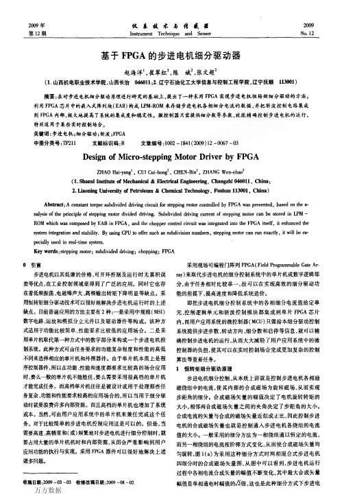
2009芷第12期仪表技术与传感器InstrumentTechniqueandSensor2009No.12基于FPGA的步进电机细分驱动器赵海洋1,崔翠红2,陈斌2,张文超2(1.山西机电职业技术学院,山西长治046011;2.辽宁石油化工大学信息与控制工程学院,辽宁抚顺113001)摘要:在对步进电机细分驱动原理进行研究的基础上,提出了一种采用FPGA实现步进电机恒转矩细分驱动的方法。
利用FPGA芯片中的嵌入式阵列块(EAB)构成LPM.ROM来存储步进电机各相细分电流的数据,并把斩波控制电路集成到FPGA内部,极大地提高了系统的集成度和稳定性。
微控制器只需提供细分数等参数,就能精确控制步进电机的运行,特别适用于某些实时控制场合。
关键词:步进电机;细分驱动;斩波;FPGA中图分类号:TP211文献标识码:B文章编号:1002—1841(2009)12—0067—03DesignofMicro-steppingMotorDriverbyFPGAZHAOHai.yan91,CUICui.hon92,CHEN—Bin2,ZHANGWen—cha02(1.ShamfiInstituteofMechanical&ElectricniEngineering,Clmngzhi046011,China;2.LiaoningUniversityofPetroleum&ChemicalTechnology,Fushun113001,China)Abstract:Aconstanttorquesubdivideddrivingcircuitforsteppingmotoreon”oHedbyFPGAWaspresented,basedonthea‘nalysisoftheprincipleofsteppingmotordivideddriving.SubdivideddrivingcurrentofsteppingmotorcanbestoredinLPM—ROMwhichWascomposedbyEABinFPGA,andthechoppercontrolcircuitWagintegratedintotheFPGAitself,itenhancedthesystemintegrationandstability.ByusingCPUtOoffersuchassubdivisionnumbers,steppingmotorCanrunexactly,itwillbee8。
HIP4080AIBZ;HIP4080AIPZ;HIP4080AIP;HIP4080AIBZT;HIP4080AIBT;中文规格书,Datasheet资料

Copyright Harris Corporation 1995, Copyright Intersil Americas Inc. 2003, 2004. All Rights Reserved
All other trademarks mentioned are the property of their respective owners.
1 /
CAUTION: These devices are sensitive to electrostatic discharge; follow proper IC Handling Procedures.
1-888-INTERSIL or 321-724-7143 | Intersil (and design) is a registered trademark of Intersil Americas Inc.
CHARGE PUMP
DIS 3
LEVEL SHIFT AND LATCH
TURN-ON DELAY
OUT 5
IN+ 6
+
IN_ 7
-
HDEL 8
LDEL 9
VSS 4
TURN-ON DELAY
AHB 10
HIP4081AIBZ中文资料

Thermal Information
Thermal Resistance (Typical, Note 1) θJA (°C/W) SOIC Package . . . . . . . . . . . . . . . . . . . . . . . . . . . . . 85 DIP Package . . . . . . . . . . . . . . . . . . . . . . . . . . . . . . 75 Storage Temperature Range . . . . . . . . . . . . . . . . . . . -65°C to 150°C Operating Max. Junction Temperature . . . . . . . . . . . . . . . . . . 125°C Lead Temperature (Soldering 10s)). . . . . . . . . . . . . . . . . . . . . 300°C (For SOIC - Lead Tips Only
AHB 10 HIGH VOLTAGE BUS ≤ 80VDC
UNDERVOLTAGE
CHARGE PUMP
LEVEL SHIFT AND LATCH
DRIVER 11
AHO CBS AHS 12
VDD 16 AHI 7 TURN-ON DELAY
DBS DIS 3 15 VCC
TO VDD (PIN 16)
NOTE: Intersil Pb-free products employ special Pb-free material sets; molding compounds/die attach materials and 100% matte tin plate termination finish, which is compatible with both SnPb and Pb-free soldering operations. Intersil Pb-free products are MSL classified at Pb-free peak reflow temperatures that meet or exceed the Pb-free requirements of IPC/JEDEC J Std-020B.
常用全桥芯片

全桥芯片是电力电子应用中常用的一种芯片,常用于直流电机的驱动、电源的开关控制等应用。
以下是几种常用的全桥芯片:
IR2110:国际整流器(International Rectifier)公司的一种全桥驱动芯片,主要用于高频交流电源、电机驱动等应用,具有高速开关、低通信损失等特点。
IRS2186:英飞凌半导体(Infineon)公司的一种全桥驱动芯片,可用于高功率直流电机驱动、交流电源等应用,具有内置过流保护、电源电压过高/过低保护等特点。
HIP4081A:意法半导体(STMicroelectronics)公司的一种高性能全桥驱动芯片,可用于大功率电机驱动、电源开关等应用,具有高速响应、低输入电流等特点。
LM5104:德州仪器(Texas Instruments)公司的一种全桥驱动芯片,主要用于高电压电源、电机驱动等应用,具有快速反应、低反馈电流等特点。
FAN7380:Fairchild半导体公司的一种高速全桥驱动芯片,主要用于电源开关、电机驱动等应用,具有短路保护、低功耗等特点。
HIP4084中文资料
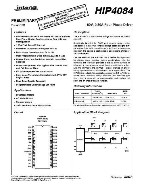
CAUTION: These devices are sensitive to electrostatic discharge; follow proper IC Handling Procedures.1-888-INTERSIL or 321-724-7143Intersil (and design) is a registered trademark of Intersil Americas Inc.File NumberTRUTH TABLEINPUT OUTPUTALI, BLI, CLI, DLI AHI, BHI, CHI, DHI UVLO/EN R DEL ALO, BLO,CLO, DLOAHO, BHO,CHO, DHOX X0X00 1X1>100mV10 001X01 011X00 101<100mV11 NOTE:X signifies that input can be either a “1” or “0”.Pin DescriptionsPINNUMBER SYMBOL DESCRIPTION2 27 17 14AHBBHBCHBDHB(xHB)High-side Bootstrap supplies. One external bootstrap diode and one capacitor are required for each. Connect cathode of bootstrap diode and positive side of bootstrap capacitor to each xHB pin.3 5 10 12AHIBHICHIDHI(xHI)High-Side Logic Level Inputs. Logic at these three pins controls the three high-side output drivers, AHO (Pin 1), BHO (Pin 26) and CHO (Pin 18) and DHO (Pin 15). When xHI is low, xHO is high. When xHI is high, xHO is low.Unless the dead time is disabled by connecting R DEL (Pin 8) to ground, the low side input of each phase will override the corresponding high side input on that phase. If R DEL is tied to ground, dead time is disabled and the outputs follow the inputs. Care must be taken to avoid shoot-through in this application. EN (Pin 9) also over-rides the high side inputs. xHI can be driven by signal levels of 0V to 15V (no greater than V DD). An internal 100µA pull-up to V DD will hold each xHI high if the pins are not driven.4 6 11 13ALIBLICLIDLI(xLI)Low-Side Logic Level Inputs. Logic at these three pins controls the three low-side output drivers ALO (Pin 24), BLO (Pin 23) and CLO (Pin 21) and DLO (Pin 20). If the upper inputs are grounded then the lower inputs controls both xLO and xHO drivers, with the dead time set by the resistor at R DEL (Pin 8). EN (Pin 9) high level input overrides xLI, forcing all outputs low. xLI can be driven by signal levels of 0V to 15V (no greater than V DD). An internal 100µA pull-up to V DD will hold xLI high if these pins are not driven.7V SS Ground. Connect the sources of the low-side power MOSFETs to this pin.8R DEL Dead Time Setting. Connect resistor from this pin to V DD to set timing current that defines the dead time be-tween drivers. All drivers turn-off with no adjustable delay, so the R DEL resistor guarantees no shoot-through bydelaying the turn-on of all drivers. When R DEL is tied to V SS, both upper and lowers can be commanded onsimultaneously. While not necessary in most applications, a decoupling capacitor of 0.1µF or smaller may beconnected between R DEL and V SS.9RUV/EN A resistor can be connected between this pin and V SS to program the under voltage set point. With this pin not connected the undervoltage setpoint is typically 6.6V. When this pin is tied to V DD, the undervoltage setpoint istypically 6.2V. With this pin tied to V SS, all six outputs are taken low, overriding all other inputs.1 26 18 15AHOBHOCHODHO(xHO)High-Side Outputs. Connect the gates of the high-side power MOSFETs to these pins.28 25 19 16AHSBHSCHSDHS(xHS)High-Side Source connection. Connect the sources of the high-side power MOSFETs to these pins. The nega-tive side of the bootstrap capacitors should also be connected to these pins.22V DD Positive supply. De-couple this pin to V SS (Pin 7).24 23 21 20ALOBLOCLODLO(xLO)Low-Side Outputs. Connect the gates of the low-side power MOSFETs to these pins.NOTE:x = A, B, C and DAbsolute Maximum Ratings T A=25o C Thermal InformationSupply Voltage, V DD . . . . . . . . . . . . . . . . . . . . . . . . . . -0.3V to 16V Logic I/O Voltages . . . . . . . . . . . . . . . . . . . . . . .-0.3V to V DD +0.3V Voltage on xHS. . . . . . . . .-6V (Transient) to +85V (-40o C to 150o C) Voltage on xHB. . . . . . . . . . . . . . . . . . . . .V xHS -0.3V to V xHS +V DD Voltage on xLO. . . . . . . . . . . . . . . . . . . . . . V SS -0.3V to V DD +0.3V Voltage on xHO . . . . . . . . . . . . . . . . . . . .V xHS -0.3V to V xHB +0.3V Phase Slew Rate . . . . . . . . . . . . . . . . . . . . . . . . . . . . . . . . . .20V/ns Operating ConditionsSupply Voltage, V DD . . . . . . . . . . . . . . . . . . . . . . . . .+7.0V to +15V Voltage on V xHS. . . . . . . . . . . . . . . . . . . . . . . . . . . . . . . . .0V to 80V Voltage on xHB. . . . . . . . . . . . . . . . . . . . . . . . . . . . . . . .V xHS + V DD Thermal Resistance (Typical, Note 1)θJA (o C/W) SOIC Package. . . . . . . . . . . . . . . . . . . . . . . . . . . . . 75o C PDIP Package. . . . . . . . . . . . . . . . . . . . . . . . . . . . . 65o C Maximum Junction Temperature. . . . . . . . . . . . . . . . . . . . . . .150o C Maximum Storage Temperature Range . . . . . . . . . .-65o C to 150o C Maximum Lead Temperature (Soldering 10s). . . . . . . . . . . . .300o C (SOIC - Lead Tips Only)Operating Ambient Temperature Range. . . . . . . . . .-40o C to 105o C Operating Junction Temperature Range . . . . . . . . .-40o C to 105o CCAUTION: Stresses above those listed in “Absolute Maximum Ratings” may cause permanent damage to the device. This is a stress only rating and operation of the device at these or any other conditions above those indicated in the operational sections of this specification is not implied.NOTES:1.θJA is measured with the component mounted on an evaluation PC board in free air.2.All voltages are relative to VSS unless otherwise specified.3.x = A, B, C, and D. For example, xHS refers to AHS, BHS, CHS, and DHS.Electrical Specifications V DD = V xHB = 12V, V SS = V xHS = 0V, R DEL = 20K, UVLO/EN = ∞, Gate Capacitance (C GATE) = 1000pFPARAMETER TEST CONDITIONST J = 25o CT J = -40o C TO150o CUNITS MIN TYP MAX MIN MAXSUPPLY CURRENTS AND UNDER VOLTAGE PROTECTIONV DD Quiescent Current xHI=5V,xLI=5V34526mA V DD Operating Current f = 20kHz, 50% Duty Cycle89.512713 mA xHB On Quiescent Current xHI = 0V-4080-100µA xHB Off Quiescent Current xHI = V DD0.60.8 1.30.5 1.4mA xHB Operating Current f = 20kHz, 50% Duty Cycle0.70.9 1.3 2.0mA Q PUMP Output Voltage No Load11.512.51410.514.5V Q PUMP Output Current V xHB = 10V-100130-140µA xHB, xHS Leakage Current V xHS = 80V, V xHB = 93V72445-50µA V DD Rising Undervoltage Threshold R UV Open 6.27.18.0 6.18.1V V DD Falling Undervoltage Threshold R UV Open 5.75 6.67.5 5.67.6V Minimum Undervoltage Threshold R UV = V DD5 6.2 6.8 4.9 6.9V INPUT PINS: ALI, BLI, CLI, DLI, AHI, BHI, CHI, DHI, AND ENLow Level Input Voltage-- 1.0-0.8V High Level Input Voltage 2.5-- 2.7-V Input Voltage Hysteresis-35---mV Low Level Input Current V IN = 0V6010013555140µA High Level Input Current V IN = 5V-1-1-1010µA GATE DRIVER OUTPUT PINS: ALO, BLO, CLO, DLO, AHO, BHO, CHO, AND DHOLow Level Output Voltage (V OUT-V SS)I SINKING = 30mA-100--200mV Peak Pulse Pullup Current V OUT 0V to 5V0.30.50.7- 1.0APeak Pulse Pulldown CurrentV OUT 12V to 4V0.71.11.50.51.7ASwitching Specifications V DD = V xHB = 12V, V SS = V xHS = 0V, R DEL = 10K, Gate Capacitance (C GATE ) = 1000pFPARAMETERTEST CONDITIONST J = 25o CT J = -40o C TO150o C UNITSMINTYPMAXMINMAXTURN ON DELAY AND PROPAGATION DELAY Dead TimeR DEL = 100K 3.8 4.5637µs R DEL = 10K0.380.50.650.30.7µs Dead Time Channel Matching R DEL = 10K -715-20%Lower Turn-Off Propagation Delay (xLI-xLO)No Load-2550-70nsUpper Turn-Off Propagation Delay (xHI-xHO)No Load -5580-100nsLower Turn-On Propagation Delay (xLI-xLO)No Load -4085-100nsUpper Turn-On Propagation Delay (xHI-xHO)No Load -75110-150nsRise Time C GATE = 1000pF -2040-50ns Fall TimeC GATE = 1000pF-1020-25ns Turn-On Input Pulse Width 50--50-ns Turn-Off Input Pulse Width50--50-ns Disable (EN) Turn-Off Propagation Delay (EN - xLO)-508090nsDisable (EN) Turn-Off Propagation Delay (EN - xHO)-75100-125nsEnable to Lower Turn-On Propagation Delay (EN - xLO)-5080-100nsEnable to Upper Turn-On Propagation Delay (EN- xHO)R DEL = 10K - 1.22-3µsRefresh Pulse Width (xLO)375580900350950µsElectrical SpecificationsV DD = V xHB = 12V, V SS = V xHS = 0V, R DEL = 20K, UVLO/EN = ∞, Gate Capacitance (C GATE ) = 1000pFPARAMETERTEST CONDITIONS T J = 25o CT J = -40o C TO150o C UNITS MIN TYP MAX MIN MAX。
88761 Electronic, 2 C #22 Str TC, FEP Ins, OS, FEP
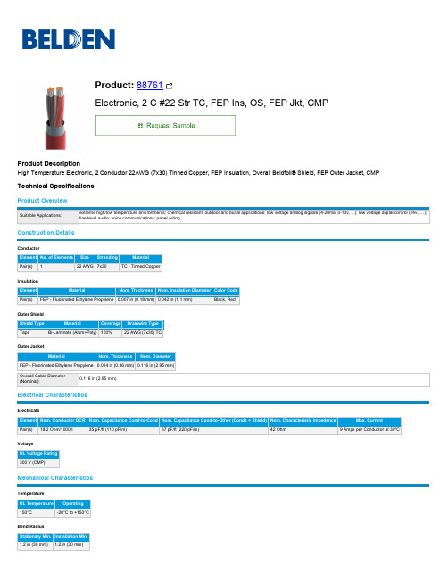
22 AWG (7x30) TC
Outer Jacket
Material
Nom. Thickness Nom. Diameter
FEP - Fluorinated Ethylene Propylene 0.014 in (0.36 mm) 0.116 in (2.95 mm)
Overall Cable Diameter (Nominal):
Temperature
UL Temperature Operating
150°C
-20°C to +150°C
Bend Radius Stationary Min. Installation Min. 1.2 in (30 mm) 1.2 in (30 mm)
Max. Pull Tension: Bulk Cable Weight:
History
Update and Revision:
Revision Number: 0.535 Revision Date: 01-20-2023
Part Numbers
Variants
Item #
Color Putup Type Length
UPC
Footnote
88761 002100 Red Reel
Max. Current
Pair(s) 18.2 Ohm/1000ft
35 pF/ft (110 pF/m)
67 pF/ft (220 pF/m)
42 Ohm
9 Amps per Conductor at 30ºC
Voltage UL Voltage Rating 300 V (CMP)
Mechanical Characteristics
常用栅极驱动芯片

常用栅极驱动芯片常用栅极驱动芯片是一种用于驱动功率MOSFET(金属氧化物半导体场效应晶体管)的集成电路。
它们在各种应用中起着关键的作用,例如交流电源、电机驱动、电力电子等领域。
本文将介绍几种常见的栅极驱动芯片,并讨论它们的特点和应用。
1. IR2110IR2110是一种高性能MOSFET和IGBT驱动芯片。
它具有低功耗、高速驱动和可靠性高的特点。
IR2110的输出极性可调,并且具有低反馈电流特性,以提高系统的效率。
该芯片适用于高频应用,如电力电子和电机驱动。
2. IRS21844IRS21844是一种高电压、高速栅极驱动芯片。
它具有高达600V的驱动电压和2A的驱动能力,适用于高压应用。
IRS21844采用了高速低功耗的逻辑输入,能够实现快速的开关操作,适用于高频电源和电机控制系统。
3. TC4420TC4420是一种高性能MOSFET和IGBT驱动芯片。
它具有低功耗、高速驱动和高电流驱动能力。
TC4420的输入电压范围广,适用于各种逻辑电平驱动。
该芯片具有短路保护和过温保护功能,可以提高系统的可靠性。
TC4420广泛应用于电力电子、电机驱动和变频器等领域。
4. MAX4420MAX4420是一种高性能MOSFET和IGBT驱动芯片。
它具有低功耗、高速驱动和低电压逻辑输入的特点。
MAX4420的输出极性可调,适用于各种应用。
该芯片具有短路保护和过温保护功能,可以提高系统的可靠性。
MAX4420适用于低电压应用,如电池供电系统和便携式设备。
5. HIP4081AHIP4081A是一种高性能MOSFET和IGBT驱动芯片。
它具有低功耗、高速驱动和大电流驱动能力。
HIP4081A的输入电压范围广,适用于各种逻辑电平驱动。
该芯片具有过温保护和短路保护功能,可以提高系统的可靠性。
HIP4081A广泛应用于电力电子、电机驱动和电源管理等领域。
总结起来,常用栅极驱动芯片是一类关键的集成电路,用于驱动功率MOSFET和IGBT。
JUMO 温度限制器和温度监测器 J TB TW 产品说明说明书

Page 1/7JUMO GmbH & Co. KGDelivery address:Mackenrodtstraße 14,36039 Fulda, GermanyPostal address:36035 Fulda, Germany Phone:+49 661 6003-0Fax:+49 661 6003-607e-mail:Internet:JUMO Instrument Co. Ltd.JUMO HouseTemple Bank, RiverwayHarlow, Essex CM 20 2TT, UK Phone:+44 1279 635533Fax:+44 1279 635262e-mail:Internet:JUMO PROCESS CONTROL INC.885 Fox Chase, Suite 103Coatesville PA 19320, USA Phone:610-380-80021-800-554-JUMOFax:610-380-8009e-mail:Internet:J TB/TWTemperature limiter, temperature monitorwith LC display for mounting on 35mm DIN railsBrief descriptionThe J TB/TW is a freely programmable temperature limiting device.The measurement input is freely configurable for resistance thermometers and thermo-couples, as well as for current and voltage signals.TB/TWs monitor thermal processes in systems for a set limit value. If this is exceeded, the built-in relay switches the system to a safe operational state and the LED K1 lights up.When the system returns to the o.k. region, the reset button (on the TB) has to be released manually using an appropriate tool.The TW, on the other hand, is reset automatically without any external action.The 4.5V/20mA logic output produces a pre-alarm signal at an adjustable temperature be-fore reaching the limit value, which is additionally indicated via the LED K2.TB/TWs are mounted on DIN rails and wired up by means of screw terminals with 2.5mm²max. conductor cross-section.A PC setup program is available as an accessory, which can be used to set and store probe type, range, output action and inhibits.Overview of functionType 701140/ …Key featuresk Setup program for configuring and archiving via PC k Clear, easy-to-read alphanumerical display k Digital input filter with adjustable filter time constant k Short 90 msec sampling intervalk Pre-alarm adjustable as absolute value or relative to limit value k Wide supply voltage range 110 — 240V AC +10% /-15%V k Configurable as TB or TW k 17 linearizations can be setk Internal and external locking options k2xPt100 input for differential measurementTechnical dataInput for resistance thermometer Input for thermocouple Analog input for DC voltage, DC currentLogic input Measuring circuit monitoringDesignationRangeAccuracy 1Pt100 EN 60751-200to +850°C0.1%KTY11-6 PTC -50to +150 °C 1%Pt1000 DIN -200to +850°C0.1%Connection circuit 2-, 3-wire Sampling interval 90 msecInput filter 2nd order digital filter; filter constant adjustable from 0to 100sec Special features 2xPt100 for differential measurement, display can also be programmed in °FDesignationRangeAccuracy 1Fe-Con L DIN 43710-200to +900°C 0.4%Fe-Con J EN60584-200to +1200°C0.4%Cu-Con U DIN 43710-200to +600°C 0.4%Cu-Con T EN60584-200to+400°C0.4%NiCr-Ni K EN 60584-200to +1372°C 0.4%NiCrSi-NiSi N EN 60584-100to +1300°C0.4%Pt10Rh-Pt S EN 605840to +1768°C 0.4%Pt13Rh-Pt R EN 605840to +1768°C 0.4%Pt30Rh-Pt6Rh B EN60584+300to +1820°C0.4%W3Re-W25Re D 0to +2495°C0.4%Cold junctionPt100 internalCold junction accuracy ± 1°C Sampling interval 90 msecInput filter 2nd order digital filter; filter constant adjustable from 0to 100secSpecial featurescan also be programmed in °F1.The accuracy refers to the maximum range span.With smaller ranges and shorter spans, the linearization accuracy is reduced.Range Accuracy Input resistance 0—20mA 4—20mA 0.1%R E < 4 Ω0—10V 2—10V 0.1%R E > 100 k ΩScalingfreely programmable within the limitsSampling interval 90 msecInput filter 2nd order digital filter; filter constant adjustable from 0—100secConnection Function Floating contactUnlocking, key locking, level locking are configurableResistance thermometer and KTY11-6Thermocouple Current / voltage Over/underrange is recognized is recognized is recognizedProbe/lead break is recognized is recognizedis recognized with 4—20mA and 2—10VProbe short-circuitis recognizedis recognized with twin thermocouples onlyis recognized with 4—20mA and 2—10VSupplySupply voltage 20 — 53V AC/DC, 48 — 63 Hz110—240V AC +10% /-15%Power consumption 5 VAOutputsRelay, no contact protection circuit150,000 operations at a contact rating of 3A/230V 50Hz resistive load Logic output 4.5V/20mA logic signal, short-circuit proofSwitching action at limit valueTest voltages to EN 60730, Part 1Electrical safetyClearance and creepage distances for normal environment to EN 60730-1, Table 20.1The instrument can be connected to SELV circuits.Environmental influencesHousing DimensionsType 701140/...Between input or output and supply- with supply voltage 110—240V AC +10% /-15% 3.75kV/50Hz - with supply voltage 20—53V AC/DC, 48—63 Hz2.5kV/50HzBetween mains supply and electronics and probe≥ 8 mm Between mains supply and relay ≥ 8 mm Between relay and electronics and probe≥ 8 mmAmbient temperature range 0to +55°C Storage temperature range -30to+70°CTemperature error ≤ ± 0.005% per °C deviation from 23°C 1 with resistance thermometers ≤ ± 0.01% per °C deviation from 23°C 1 with thermocouples, current, voltageClimatic conditions 75% rel. humidity, no condensationEMCEN 61326Interference emission Class BNoise immunityindustrial requirements1.All data refer to the full scale valueMaterial polyamide (PA 6.6)Screw terminals 0.2—2.5mm 2 screw terminal Mountingon 35mm x 7.5mm DIN rail to EN 50022Operating position vertical Weight160g approx.Connection diagramDIN approved probes for operation in airDIN approved probes for operation in water and oilRTDs to Data Sheet 90.2006Probe type Temperature range Nom. length mmProcess connection 90.271-F01 2 x Pt100-170 to +700°C500sliding stop flange90.272-F0171090.273-F01100090 2006/55... 2 x Pt100-170 to +700°C500sliding clamping thread G1/290 2006/55...70090 2006/55...100Thermocouples to Data Sheet 90.1006Probe type Temperature range Nom. length mmsliding stop flange 90.019-F01 2 x NiCr-Ni, Type K-35 to +800°C50090.020-F0171090.021-F01100090.019-F11 2 x Fe-Con, Type L-35 to +700°C50090.020-F1171090.021-F11100090.023-F01 2 x NiCr-Ni, Type K-35 to +1000°C50090.023-F0235590.023-F0325090.021 1 x PT10Rh-PT, Type S0 to 1300°C25090.02235590.02350090-D-021 2 x PT10Rh-PT, Type S0 to 1300°C25090-D-02235590-D-02350090.027 1 x PT30Rh-PT6Rh, Type B600 to 1500°C25090.02835590.02950090-D-027 2 x PT30Rh-PT6Rh, Type B600 to 1500°C25090-D-02835590-D-029500RTDs to Data Sheet 90.2006Probe type Temperature range Fitting length mm Process connection 90.2006/10... 1 x Pt100-40 to +400°C100G1/2 thread90.2006/10... 2 x Pt10010090.272-F02 2 x Pt100-170 to +550°C 65—670sliding clamping thread G1/2 90.272-F03 1 x Pt10065—67090.239 1 x Pt100-170 to +480°C 250G1/2 thread 90-D-239 2 x Pt10025090.239-F01 1 x Pt100-40 to +480 °C 100weld-in pocket 90.239-F1116090.239-F2122090.239-F03 1 x Pt100-40 to +400 °C 19090D239-F03 2 x Pt100-40 to +400 °C 19090.239-F02 2 x Pt100-40 to +480 °C10090.239-F1216090.239-F2222090.239-F07 3 x Pt100-40 to +400 °C10090.239-F1716090.239-F2722090.280-F30 1 x Pt100-170 to +480°C22090.280-F3116090.280-F32100Thermocouples to Data Sheet 90.1006Probe type Temperature range Fitting length mm Process connection 90.020-F02 2 x NiCr-Ni, Type K -35 to +550°C65—670sliding clamping thread G1/290.020-F03 1 x NiCr-Ni, Type K 65—67090.020-F12 2 x Fe-Con, Type L 65—67090.020-F13 1 x Fe-Con, Type L 65—67090.111-F01 1 x Fe-Con Type L -35 to +480°C 220weld-in pocket 90.111-F022 x Fe-Con Type L220Order details(1)Basic version701140JUMO temperature limiter (TB) / temperature monitor (TW)(2)Basic type extension (programmable)0151Temperature monitor, inverse0152Temperature monitor, direct0153Temperature limiter, inverse0154Temperature limiter, directX888programmable, factory-setX999programmable, configuration to customer specification1(3)Measurement input001Pt100 in 3-wire circuit003Pt100 in 2-wire circuit005Pt1000 in 2-wire circuit006Pt1000 in 3-wire circuit0242xPt100 for differential measurement037W3Re-W25Re D039Cu-Con T040Fe-Con J041Cu-Con U042Fe-Con L043Ni-CrNi K044Pt10Rh-Pt S045Pt13Rh-Pt R046Pt30Rh-Pt6Rh B048NiCrSi-NiSi N0520—20 mA0534—20 mA0630—10 V0712—10 V601KTY11-6X888programmable, factory-setX999programmable, configuration to customer specification1(4)SupplyX23110—240V AC +10% /-15%, 48—63HzX2220—53V AC/DC, 48—63Hz(5)ApprovalsX000no approvalX061UL approvalfactory-set 1. For configuration to customer specification, please specify in plain text(1)(2)(3)(4)(5)Order codeOrder example701140-888-888-22-000Standard accessory- 1 Operating ManualAccessories-Setup program-PC interface with TTL/RS232C converter and adapter (4-pole socket) for connecting the TB/TW to a PC-External reset button, Sales No. 70/97097865。
HIP4086中文资料

AHI, BHI, CHI
UV
DIS
X
X
X
1
X
X
1
X
1
X
0
0
0
0
0
0
0
1
0
0
1
0
0
0
NOTE: X signifies that input can be either a “1” or “0”.
TURN-ON DELAY
DRIVER
DEAD TIME DISABLE
20 VDD 21 ALO 6 VSS
BPC-1型电力电子技术及电机控制实验装置型电力电子技术及
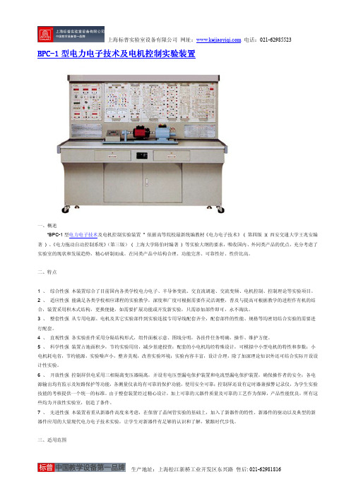
BPC BPC--1型电力电子技术及电机控制实验装置型电力电子技术及电机控制实验装置一、概述“BPC-1型电力电子技术及电机控制实验装置 ” 依据高等院校最新统编教材《电力电子技术》 ( 第四版 )( 西安交通大学王兆安编著 ) 、《电力拖动自动控制系统》(第三版) ( 上海大学陈伯时编著 ) 等实验大纲的要求,吸收国内、外同类产品的优点,充分考虑了实验室的现状和发展趋势,精心研制而成。
在同类产品中结构合理、功能完善、可靠性好、性价比高。
二、特点1 、 综合性强 本装置综合了目前国内各类学校电力电子、半导体变流、交直流调速、交流变频、电机控制、控制理论等实验项目。
2 、 适应性强 能满足各类学校相应课程的实验教学,深度和广度可根据需要作灵活调整,普及与提高可根据教学的进程作有机的结合,装置采用积木式结构,更换便捷,如需要扩展功能或开发新实验,只需添加部件即可,永不淘汰。
3 、 整套性强 从专用电源、电机及其它实验部件到实验连接专用导线配套齐全,配套部件的性能、规格等均密切结合实验的需要进行配套。
4 、 直观性强 各实验挂件采用分隔结构形式,组件面板示意、图线分明,各挂件任务明确,操作、维护方便。
5 、 科学性强 装置占地面积少,节约实验用房,减少基建投资;配套的小电机均经特殊设计,可模拟中小型电机的特性和参数;小电机耗电省,节约能源,实验噪声小,整齐美观,改善实验环境;实验内容丰富,设计合理,除了加深理论知识外还可结合实际开设设计性实验。
6 、 开放性强 控制屏供电采用三相隔离变压器隔离,并设有电压型漏电保护装置和电流型漏电保护装置,确保操作者的安全;各电源输出均有监示及短路保护等功能,各测量仪表均有可靠的保护功能,使用安全可靠;控制屏还设有定时器兼报警记录仪,为学生实验技能的考核提供一个统一的标准。
由于整套装置经过精心设计,加上可靠的元器件质量及可靠的工艺作为保障,产品性能优良,所有这些均为开放性实验室,创造了条件。
- 1、下载文档前请自行甄别文档内容的完整性,平台不提供额外的编辑、内容补充、找答案等附加服务。
- 2、"仅部分预览"的文档,不可在线预览部分如存在完整性等问题,可反馈申请退款(可完整预览的文档不适用该条件!)。
- 3、如文档侵犯您的权益,请联系客服反馈,我们会尽快为您处理(人工客服工作时间:9:00-18:30)。
2 HIP4081内部结构及技术特点
HIP4081是intersil公司推出的一款专门用于控制H桥的高频全桥驱动芯片。
采用闩锁抗干扰CMOS 制造工艺,具有独立的低端和高端输入通道,分别独立驱动4个N沟道MOS 管;输出峰值电流为2 A;芯片内部具有电荷泵和死区时间设置;悬浮电源采用自举电路,其高端工作电压可达95 V,逻辑电源电压范围6~15 V,工作频率高,可达1 MHz;具有能控制所有输入的禁止端,可方便地与外接元件形成保护电路。
图3给出HIP4081的引脚排列定义,图4显示了1/2 HIP4081(A边)的内部功能框图。
主要组成部分有:逻辑输入、使能、电荷泵、电平平移及死区时间设置等。
在图4中,ALI,AHI分别是A边的低边输入和高边输入;ALO,AHO分别是A边的低边输出和高边输出,DIS是使能输入;在另一半(B边)的内部功能图中,BLI、BHI分别是B边的低边输入和高边输入;BLO,BHO分别是B边的低边输出和高边输出。
他们之间的逻辑关系如表1所示。
3 电路实现基本原理
电路原理框如图5所示。
在图5中,Vcc?为内部逻辑电路和MOS管上臂和下臂驱动器的低压电源;Vs为H桥
供电电源,MOS管从这个电源端获得输出电流,该脚电压范围为Vcc?~+80 V;?V o1?为半桥的输出脚1,当PWM输入ALI为高,BLI为低时,该脚输出为Vs;V o2?为半桥的输出脚2,当PWM输入ALI为低,BLI为高时,该脚输出为Vs;SENSE为2个半桥下臂的共同联接点,可连接一个到Vs地的检测电阻以检测电流,该脚也可以直接连到Vs的地。
GND 为输入逻辑和Vcc?的地;PWM输入为用于输入与TTL兼容的PWM信号,占空比在0%~100%之间;DIS为用于关断4个MOS管,该脚为1时为关断,为0时使能。
3.1 电路工作逻辑时序及电机运动状态分析
在图5中,当使能端DIS处于高电平“1”时,无论ALI,BLI是“1”还是“0”,ALO,BLO,AHO,BHO都为“0”,电路处于禁止状态,电机停转。
当使能端DIS处于低电平“0”时,ALI和BLI可通过反相器分别同时接收PWM信号的高电平“1”和低电平“0”。
当ALI 为1,BLI为0时,此时,ALO为1,AHO为0,BLO为0,BHO为1,H 桥中的MOS管M1与M4导通,H桥?处于图1状态,电机顺时针旋转。
当ALI为0,BLI为1时,此时,ALO为0,AHO为1,BLO为1,BHO为0,H桥中的MOS管M3与M2导通,H桥处于图2?状态,电机逆时针旋转。
当ALI,BLI同时为0时,ALO,BLO都为0,AHO,BHO都为1,电机中没有电流流过,处于制动状态。
当ALI,BLI同时为1时,ALO,BLO都为1,AHO,BHO都为0,电机中也没有电流流过,同样处于制动状态。
其逻辑关系如表2所示。
3.2 死区时间的考虑在图5中,保证H桥上2个同侧的MOS管(M1和M2,M3和M4)不会同时导通非常重要。
如果MOS管M1和M2(或M3和M4)同时导通,那么电流就会从电源Vs正极穿过2个MOS管直接回到负极。
此时,电路中除了MOS管外没有其他任何负载,因此电路上的电流就可能达到最大值(该电流仅受电源性能限制),甚至烧坏MOS管。
基于上述原因,在实际驱动电路中要使M1与M2或M3与M4在导通时间上有一个延迟,也称死区时间。
HIP4081留有HDEL和LDEL两个端口(见图4),?用户通过外接电阻,可根据实际电路工作情况,自行定制死区时间。
死区时间与HDEL/LDEL电阻的关系如图6所示。
3.3 效率的考虑
在图5中,决定驱动电路效率的主要是以下3个因素:HIP4081的静态功耗;Vcc?电源的动态功耗;MOS管的I?2R损耗。
由于HIP4081是CMOS器件,第(1)项损耗很小,可忽略不计,第(2)项损耗虽然大一些,但远小于(3)项(尤其是满负荷输出时)。
而MOS管的I?2R由其导通电阻决定,因此选择合适的MOS管组成H桥电路,可以减少(3)项损耗。
该电路选用N沟道HEXFET Power MOSFET IRFP250N,其导通电阻为0.075 Ω,降低了导通损耗,提高了效率。
3.4 产品结构的考虑
(1)该产品结构采用厚膜混合集成技术设计,如图7?所示,在具有高导热率的AlN 陶瓷基板上通过厚膜印烧工艺制作厚膜基板,并通过基板金属化与焊接技术,将ALN基板与金属外壳进行焊接,大大提高了电路的导热能力和功率密度。
(2)在图7中,产品内部全部有源器件采用裸芯片,通过混合集成电路的二次集成工艺技术,将元器件、ALN厚膜陶瓷基板以及金属外壳组装在一起。
形成具有全密封金属外壳、外形尺寸为32 mm×32 mm×7 mm?的双列直插式厚膜混合集成产品,大大缩小了体积,减少了产品内部级连和焊点,提高了可靠性。
4 结语
这里设计的厚膜H桥电机驱动电路经过实际应用表明:该电路不仅安全可靠地实现了电机的双向转动和调速,提高了驱动电路和系统的可靠性,而且产品体积小,导热性能好,效率高,能在恶劣的使用环境下安全工作,适合军、民两用。
参考文献
[1]Intersil.Application Note AN9325\.3.2003.
[2]Intersil.HIP4081 Data Sheet\.1996.
[3]IR.IRFP250N Data Sheet\.2004.
[4]谭建成.电机控制专用集成电路\.北京:机械工业出版社,1997.
[5]谭建成.新编电机控制专用集成电路与应用\.北京:机械工业出版社,2005.
[6]吴红星.电机驱动与控制专用集成电路及应用\.北京:中国电力出版社,2006.
[7]张崇巍,李汉强.运动控制系统\.武汉:武汉理工大学出版社,2002.
[8]刘宝延,程树康.步进电动机及其驱动控制系统\.哈尔滨:哈尔滨工业大学出版社,1997.
[9]高钟毓.机电控制工程\.2版.北京:清华大学出版社,2002.
[10]王成元.电机现代控制技术\.北京:机械工业出版社,2006.
[11]谢少荣,蒋蓁,罗均,等.现代控制与驱动技术\.北京:化学工业出版社,2005.
[12]冬雷.DSP原理及电机控制系统应用\.北京:北京航空航天大学出版社,2007.。
